Embed Size (px)
Citation preview

Author: Chao XIA (ISE) Supervisor: Prof. Dr.-Ing. Klaus Solbach Prof. Dr.-Ing. Adalbert Beyer
DTIU-Outlet
Introduction Looking Through of whole Test System Working Principle of the Circuit under Test Digital to Analog Converter(DAC) MAX5100 Process of test Design of the Printed Circuit Board (PCB) Connected-condition of 3 different Connectors Principle of “Quancom” I/O Card Design of the Graphical User Interface (GUI) Test Results
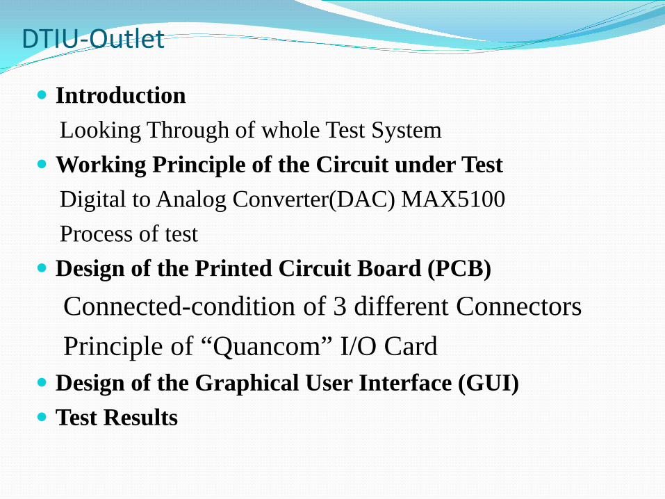
DTIU-Looking through of whole Test System
GUI RF-Inp.

DTIU-Working Principle of the Circuit under Test Bit 1-8 : Data bits Bit 9-10 : Address bits of
DAC in Switch/Modulator Bit 11-14 : Address bits of
cassette Bit 15 : Contorl bit of
switch and modulator Bit 16 : Control bit of data
writing Bit 17 : Control bit of the
outputs transparent
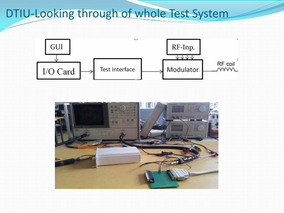
DTIU-Digital to Analog Converter(DAC)
Bit 9 Bit 10 Output A 1 0 Output B 0 0 Output C 0 1 Output D 1 1
Output A Output B Output C Output D
I I Q Q
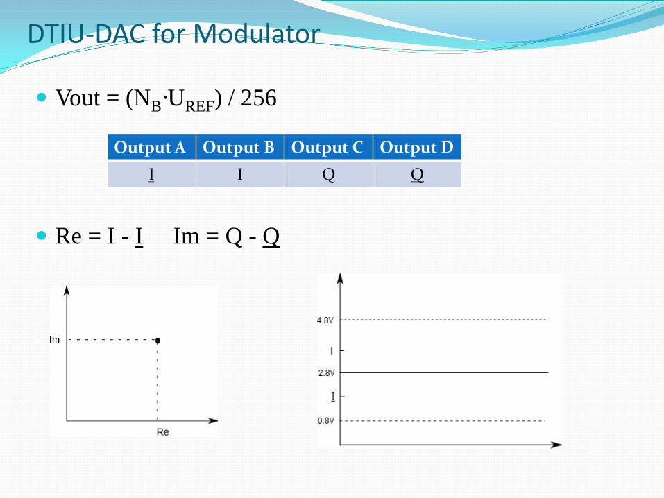
DTIU-DAC for Modulator
Vout = (NB·UREF) / 256
Re = I - I Im = Q - Q
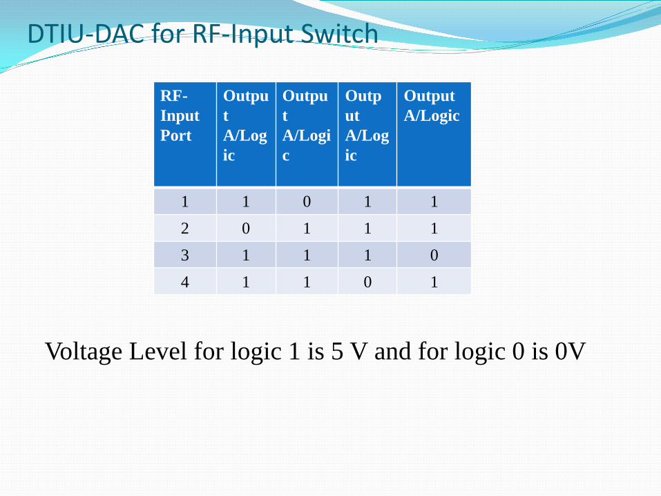
RF-Input Port
Output A/Logic
Output A/Logic
Output A/Logic
Output A/Logic
1 1 0 1 1 2 0 1 1 1 3 1 1 1 0 4 1 1 0 1
DTIU-DAC for RF-Input Switch
Voltage Level for logic 1 is 5 V and for logic 0 is 0V
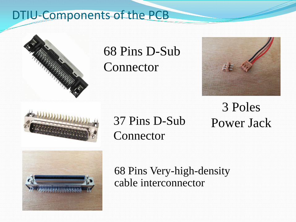
DTIU-Components of the PCB
68 Pins D-Sub Connector
37 Pins D-Sub Connector
68 Pins Very-high-density cable interconnector
3 Poles Power Jack

DTIU-Voltage Level Standard of I/O Card
Pin Configuration of the Card’s 68 Pins
Transistor-Transisitor Logic(TTL) Standard
Pin Num. 1-32 33-34 35-66 67-68
Pin Conf. I/O 1-32 GND I/O 33-64 3.3V
Logic conditon High State Low State Initial State Digital Value 1 0 -- Voltage Range >=2.4V <=0.4V 0.8V<=U<=2.4
V Voltage 3.6V 0V 1.2V

DTIU-Correponding connect-relation for 3 Connectors Logic Bits 1 2 3 4 5 6 7 8 9 68Pin D-Sub
31 32 30 28 26 24 22 20 18
37Pin D-Sub
1 2 3 4 5 6 7 8 9
VHDCI 65 31 63 29 61 27 59 25 57
Logic Bits
10 11 12 13 14 15 16 17 18 19
68Pin D-Sub
16 14 12 10 8 6 4 2 --- ---
37Pin D-Sub
10 11 12 13 14 15 16 17 +5V
-5V
VHDCI 23 55 21 53 19 51 17 1 --- ---
* VHDCI:Very-high-density cable interconnector
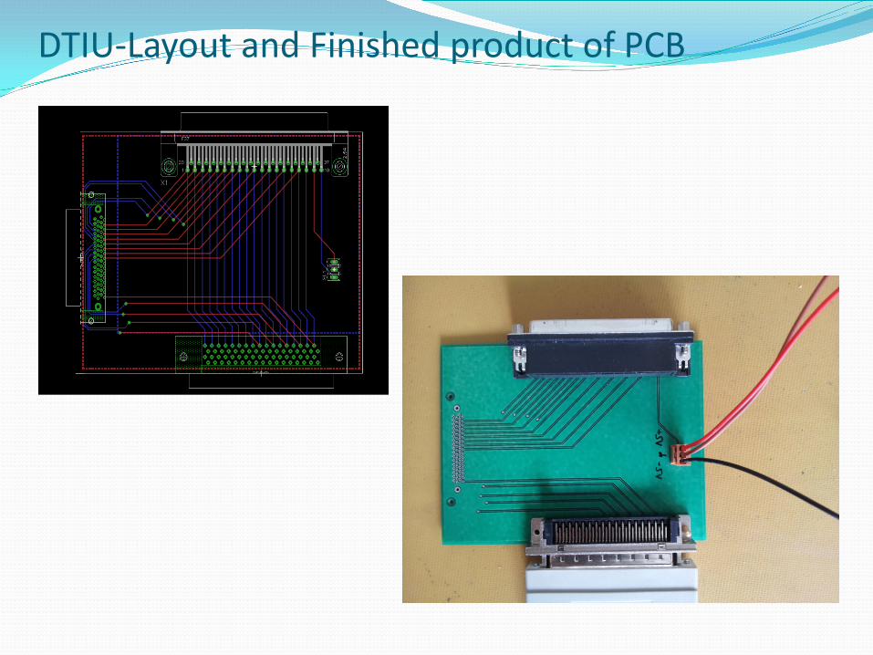
DTIU-Layout and Finished product of PCB
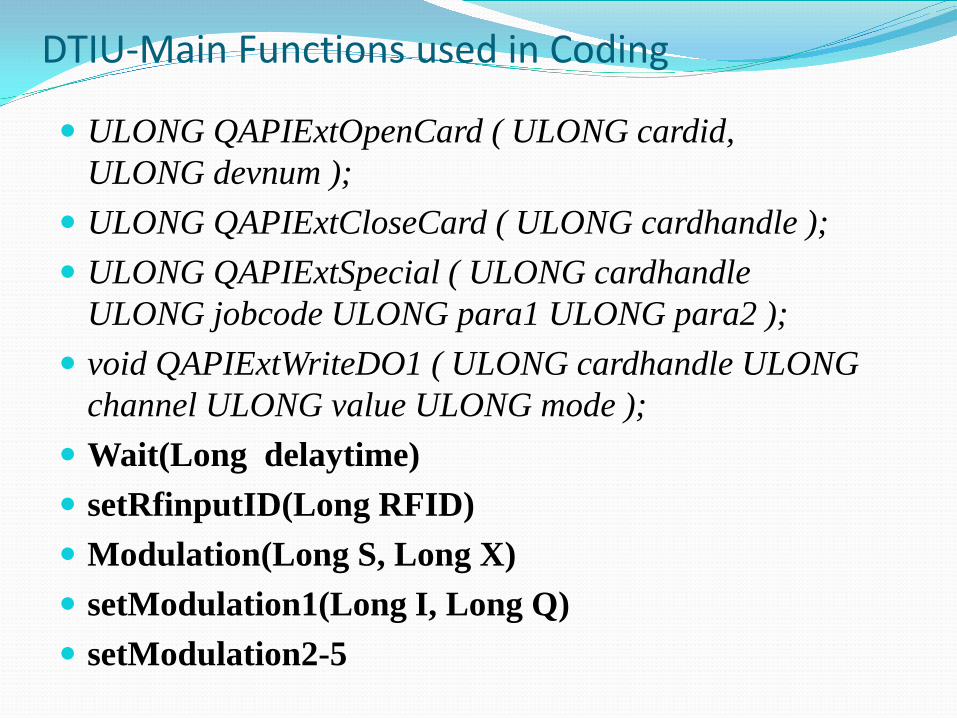
DTIU-Main Functions used in Coding
ULONG QAPIExtOpenCard ( ULONG cardid, ULONG devnum );
ULONG QAPIExtCloseCard ( ULONG cardhandle ); ULONG QAPIExtSpecial ( ULONG cardhandle
ULONG jobcode ULONG para1 ULONG para2 ); void QAPIExtWriteDO1 ( ULONG cardhandle ULONG
channel ULONG value ULONG mode ); Wait(Long delaytime) setRfinputID(Long RFID) Modulation(Long S, Long X) setModulation1(Long I, Long Q) setModulation2-5
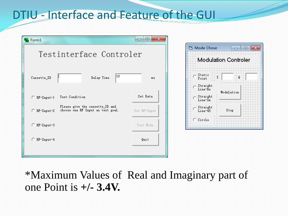
DTIU - Interface and Feature of the GUI
*Maximum Values of Real and Imaginary part of one Point is +/- 3.4V.
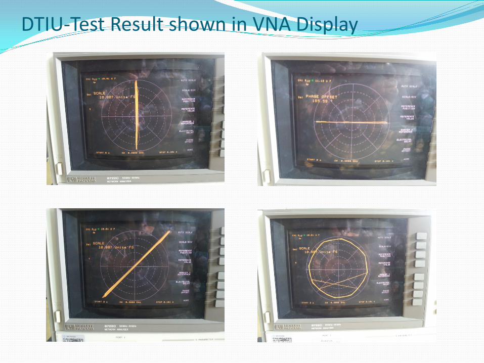
DTIU-Test Result shown in VNA Display

THANK YOU Chao XIA(Matr. 2253339) ISE [email protected]