Embed Size (px)
Citation preview

Design of Active Clamp for Fast Transient Voltage Regulator-Down (VRD)
Applications
by
Yan Ma
Thesis submitted in partial fulfillment of the requirements for the degree of
MASTER OF SCIENCE
in
ELECTRICAL ENGINEERING
in the
SCHOOL OF ENGINEERING
at the
Virginia Polytechnic Institute and State University
APPROVED:
Dec 10, 2004
Blacksburg, Virginia
Keywords: voltage regulator down, fast transient response, active clamp, error feedback
Prof. Joseph G. Tront Prof. Dong S. Ha
Prof. Alex Q. Huang, Chairman
Design of Active Clamp for Fast Transient Voltage Regulator-Down (VRD)
Applications
By
Yan Ma
Prof. Alex Q. Huang, Chairman
Electrical Engineering
(ABSTRACT)
Since the early 80s, the computer industry has undergone great expansion. Processors
are becoming faster and more powerful. Power management issues in computing systems
are becoming more and more complex and challenging. An evolution began when the
high-performance Pentium processor was driven by a non-standard, less-than-5V power
supply, instead of drawing its power from the 5V plane on the system board. A so-called
Voltage Regulator Module (VRM) is put close to the processor in order to provide the
power as quickly as possible. Nowadays, for desktop and workstation applications, VRM
input voltage has moved to the 12V output of the silver box. In the meantime,
microprocessors will run at very low voltage (below 1V), will consume up to 100A of
current, and will have dynamics of about 400A/us. In the near future, VRM will be
replaced with VRD because of the parasitic components effect. The specifications
requirements for VRD are even more challenging than VRM [1].

iii
With this kind of tight tolerance, high current and fast current slew rate, transient
response requirements for VRD design are very challenging, especially for step-down
transient. During step-down transient, there is some additional energy stored in inductor.
Traditional switching regulator like multi-phase buck can do nothing for this even by
saturating the duty cycle to 0. All of the additional energy in inductor will be dumped
into output cap and cause a large voltage spike at the output voltage. Even for step-up
transient, traditional linear control like voltage loop control can’t provide enough
bandwidth because of the slow compensation and slow slew rate of the error amplifier.
So the voltage drop is still quite large.
Comparing with traditional linear controlled switching regulator such as voltage
control and current control buck converter, active clamp has a lot of the advantages for
the transient response. With proper design, active clamp can generate a very high
bandwidth since there is no compensator needed in the control loop. Since active clamp
bypasses inductor and is connected directly to the output cap, it can quickly source and
sink current from the output cap even during the step-down transient and prevent
overshooting of the output voltage. This is the biggest advantage for active clamp
comparing with traditional linear control.
In this thesis, a new active clamp structure is proposed. Several new concepts are
proposed like non-linear Gm, built-in offset Gm, error signal feedback and AVP design.
A one-channel buck converter with new active clamp and voltage loop control is
implemented and verified using real transistors based on 0.5um CMOS process.

iv
Acknowledgements
With sincere appreciation in my heart, I would like to thank my advisor, Dr. Alex Q.
Huang for his guidance, encouragement and support during the entire course of my
graduate study and research at Virginia Tech. His knowledge, vision and creative
thinking have been the source of inspiration and invaluable help, without which none of
this would have been possible. I would also like to thank my thesis committee members
Dr. Dong S. Ha and Dr. Joseph G. Tront for their comments and reviewing my thesis.
It has been a pleasure working with my colleagues. Their kindness has made my study
enjoyable. Especially, I thank Mr. Nick Sun, Mr. Xin zhang, Mr. Xiaoming Duan, Ms. Li
Ma, Mr. Jinseok Park, Mr. Ding Li, Mr. Hongtao Mu, Mr. Ali Hajjiah, Ms. Yan Gao, Ms.
Ji Pan and Ms. Maggie Xiong for their friendship and help.
I would like to thank my family. My parents have always stressed the importance of
hard work and dedication, without which I may not be where I am today.
Special thanks to my husband, Haifei Deng, who has always been there with his love,
understanding and support during the past years.

v
Table of Contents
(ABSTRACT) ................................................................................................................................ ii
Chapter 1: Introduction........................................................................................................... 1
1.1. Background..................................................................................................................... 1
1.2. Trends of the VRD 10.x.................................................................................................. 4
1.2.1. Advantages and disadvantages of traditional switching regulator.......................... 7
1.2.2. Advantages and disadvantages of active clamp...................................................... 9
1.3. Objective of this work................................................................................................... 10
1.4. Outline of the thesis ...................................................................................................... 10
Chapter 2: Review of existing active clamps........................................................................ 12
2.1. General active clamp structure...................................................................................... 12
2.2. Active clamp structure from Berkeley.......................................................................... 14
2.3. Transient voltage clamp concept .................................................................................. 17
2.4. Summary ....................................................................................................................... 18
Chapter 3: New active clamp design and modeling ............................................................ 19
3.1. New active clamp structure........................................................................................... 19
3.2. Comparison between new active clamp structure and other structures ........................ 22
3.3. AVP implementation .................................................................................................... 25
3.4. Error feedback concept ................................................................................................. 27
3.5. Summary ....................................................................................................................... 30
Chapter 4: Sub-blocks design and system implementation................................................ 31
4.1. Introduction................................................................................................................... 31
vi
4.2. Non-linear Active Clamp Design.................................................................................. 32
4.2.1. Asymmetric Gm block with built-in offset design ............................................... 33
4.2.2. Non-linear Gm block design................................................................................. 36
4.2.3. Non-linear active clamp based on current mirrors................................................ 39
4.2.4. Final Schematic and simulation results................................................................. 40
4.2.5. Summary ............................................................................................................... 42
4.3. AVP, Error Signal Feedback implementation .............................................................. 43
4.4. High speed synchronous driver design ......................................................................... 44
4.4.1. Dead-time control ................................................................................................. 45
4.4.2. High voltage level shift design ............................................................................. 46
4.4.3. High side gate signal sensor design ...................................................................... 47
4.4.4. High-speed synchronous driver design................................................................. 48
4.5. Single channel voltage loop design............................................................................... 50
4.5.1. Loop compensation design ................................................................................... 51
4.5.2. Schematic and verification.................................................................................... 54
4.6. System implementation and verification ...................................................................... 56
4.7. Summary ....................................................................................................................... 58
Chapter 5: Summary and future work................................................................................. 60
5.1. Summary ....................................................................................................................... 60
5.2. Future work................................................................................................................... 61
References.................................................................................................................................... 62
Vita………………………………………………………………………………………………66

vii
List of Figures
Figure 1-1 Power hungry CPU ....................................................................................................... 1
Figure 1-2 Power path for CPU ...................................................................................................... 2
Figure 1-3 Intel roadmap for desktop VRD.................................................................................... 3
Figure 1-4 The Lump Model of the 2004 Power Delivery Path .................................................... 4
Figure 1-5 AVP and VRD10.x load line......................................................................................... 5
Figure 1-6 Transient response requirement for VRD ..................................................................... 6
Figure 1-7 Inductor current slew rate and output voltage drop ...................................................... 8
Figure 1-8 Inductor current slew rate and output voltage drop for step down transient................. 9
Figure 2-1 General structure for active clamp .............................................................................. 12
Figure 2-2 Comparison between active clamp and other fast transient structures ....................... 13
Figure 2-3 Functional block diagram for Berkeley’s active clamp .............................................. 14
Figure 2-4 Schematic of pull-up Gm block .................................................................................. 15
Figure 2-5 Transfer characteristics of active clamp...................................................................... 16
Figure 2-6 Functional block diagram for transient voltage clamp structure................................. 17
Figure 3-1 Structure of new active clamp with linear voltage control loop ................................. 19
Figure 3-2 Structure of new active clamp..................................................................................... 20
Figure 3-3 Transfer characteristics for the new active clamp....................................................... 21
Figure 3-4 Transfer characteristics for linear control ................................................................... 22

viii
Figure 3-5 Transfer characteristics for bang-bang controlled active clamp ................................. 23
Figure 3-6 Transfer characteristics of Berkeley’s active clamp structure .................................... 24
Figure 3-7 AVP implementation in new active clamp structure................................................... 25
Figure 3-8 AVP reduce the total voltage spike............................................................................. 26
Figure 3-9 Transient waveform for linear control ........................................................................ 27
Figure 3-10 Settling time problem without error feedback .......................................................... 28
Figure 3-11 Transient waveform with error signal feedback........................................................ 29
Figure 4-1 System diagram of the new active clamp structure with linear control ...................... 31
Figure 4-2 New active clamp structure......................................................................................... 32
Figure 4-3 Symmetric Gm block .................................................................................................. 33
Figure 4-4 Asymmetric Gm block ................................................................................................ 34
Figure 4-5 Asymmetric Gm block with Ioffset ................................................................................ 35
Figure 4-6 Non-linear Gm block diagram .................................................................................... 36
Figure 4-7 Transfer characteristics of non-linear Gm block diagram........................................... 38
Figure 4-8 Non-linear active clamp block diagram (pull-up path) ............................................... 39
Figure 4-9 Schematic of the non-linear Gm block........................................................................ 40
Figure 4-10 Schematic of the whole non-linear active clamp block ............................................ 41
Figure 4-11 Simulated transfer characteristics of non-linear active clamp .................................. 41
Figure 4-12 Feed back signal generation block ............................................................................ 43

ix
Figure 4-13 Synchronous driver in a single-phase buck converter............................................... 44
Figure 4-14 Level shift for high side driver................................................................................ 46
Figure 4-15 Final schematic for the synchronous driver .............................................................. 48
Figure 4-16 Simulated time diagram for synchronous driver....................................................... 49
Figure 4-17 System block diagram for single-phase linear voltage control ................................. 50
Figure 4-18 Compensator used in the linear controlled single-phase buck .................................. 51
Figure 4-19 Compensation design based on MathCAD ............................................................... 53
Figure 4-20 Final schematic for the single-phase voltage control buck ....................................... 54
Figure 4-21 Simulated waveform for single-phase voltage control buck without active
clamp..................................................................................................................................... 55
Figure 4-22 The final test bench for the whole system................................................................. 56
Figure 4-23 Transient response with both linear control loop and active clamp.......................... 57
Figure 4-24 Transient response with and without active clamp for different bulk cap ................ 58

x
Table 4-1 Specification of the single-phase buck ......................................................................... 51

1
Chapter 1: Introduction
1.1. Background
Figure 1-1 Power hungry CPU
Computer is playing and will continue to play an important role in our everyday life.
We are depending more and more on the computer and spending more and more time
before computers. As shown in Figure 1-1, behind the black computer box, there is an
important part called CPU. It is the core of the whole system and the heart for the whole
computer. With the computer becoming more and more powerful, the CPU is becoming
more and more complex and consuming more and more power. The power management
for computer becomes very challenging. Since the power requirements for CPU is very
critical, a dedicated power module called Voltage Regulator Module is developed to
provide power for the CPU. Figure 1-2 is the power path for CPU[2]. AC power supply
will be fed into silver box first. A 5 to 12 volts bus voltage will be generated and be fed
into VRM as the input voltage. A 300kHz multi-phase buck voltage regulator is used as
VRM to provide a constant high quality voltage for the CPU.
2
Plug-in VRM
Processor Socket
Embedded VRM
Plug-in VRM
Processor Socket
Embedded VRM
AC Silver Box
VRMVRM5V 12V
uPuPAC Silver Box
VRMVRM5V 12V
uPuPuPuP
Multiphase buck converter
Q2
Q1
Vin Co ProcessorLoad
Q4Q3
Q2
Q1
Vin Co ProcessorLoad
Q4Q3
Multiphase buck converter
Q2
Q1
Vin Co ProcessorLoad
Q4Q3
Q2
Q1
Vin Co ProcessorLoad
Q4Q3
Figure 1-2 Power path for CPU
In order to save cost and keep good maintenance, VRM is built as a plug-in module
first. In case it were broken, a new module can be easily plugged in. However, a plug-in
module will generate a lot of parasitic components, which is playing more and more
negative effect in the quality of the VRM output. Nowadays, Voltage Regulator Down
(VRD) replaces VRM. Since VRD is embedded on the motherboard, there are less
parasitic components on the power delivery bus [3]. In this thesis, active clamp is
designed based on VRD application.

3
Figure 1-3 Intel roadmap for desktop VRD
Figure 1-3 is Intel roadmap for desktop VRD [4]. From the picture, we can see that the
output voltage is going to drop down lower and lower to 0.8 in 2005. The output current
is going to rise up to 130A and slew rate di/dt is going to be 400A/us. Besides this, the
output voltage tolerance is going to be 80mV and even smaller. With this kind of low
output voltage, high current, high slew rate and tight tolerance, the design for VRD
application becomes very challenging, especially for transient response.
4
1.2. Trends of the VRD 10.x
SocketSocket
Socket
Processor
OLGAOsconOscon
*information from IntelFor 478-pin socket
Specs :1.2V/90A (Prescott uP)
Loop 1Loop 1
D
Loop 3
Bulk Cap
D
Loop 3
Bulk Cap
C
Loop 2
Sense point
Decoupling cap in the cavity
C
Loop 2
Sense point
Decoupling cap in the cavity
C
Loop 2
Sense point
Decoupling cap in the cavity
io
AB
Loop 0
Packaging cap
Cap on die
io
AB
Loop 0
Packaging cap
Cap on die
VRVR CPUCPUReference: “Power delivery path analysis” by Y.C. Ren and G. Yao
Figure 1-4 The Lump Model of the 2004 Power Delivery Path
Figure 1-4 is the Lump Model of the 2004 Power Delivery Path [3]. We will see that it
can be separated into four loops and there are some parasitic components in the delivery
path. The first loop in the path is the power stage of the multi-phase buck converter. A
big bulk cap is needed here as the output cap. From the output cap to the cavity
underneath VRD, there are a parasitic inductor and a resistor. A decoupling cap with ESR
and ESL is sitting in the cavity underneath VRD. From the cavity to CPU package, a
socket and OLGA are used. Another inductor and ESR are generated. Inside the CPU
package, another decoupling cap with ESR and ESL is used. Each loop in this delivery
path is going to generate a voltage spike in the transient voltage waveform at sensing

5
point C. Those parasitic components induce a lot of trouble in the VRD design when
considering the efficiency, transient response and voltage tolerance.
165mV
time0A
90AIO
VO
2×TOB
50mV25μs
165mV
time0A
90AIO
VO
2×TOB2×TOB
50mV50mV25μs
Final designFinal designFinal design
VRD 10.0 can tolerate higher voltage spikes in step-down transient response.
VRD 10.0 Specification
VvrmMIN
VvrmMAX
VO
IO
0A 20A 40A 60A 80A 100A1.32V
1.35V
1.38V
1.41V
1.44V
1.47V
1.50V
1.53V
VID=1.5V
2×TOB
(For Intel® Prescott Processor)
RLL=1.3mΩ
VRD 10.0 Specification
VvrmMIN
VvrmMAX
VvrmMIN
VvrmMIN
VvrmMAX
VvrmMAX
VO
IO
0A 20A 40A 60A 80A 100A0A 20A 40A 60A 80A 100A1.32V
1.35V
1.38V
1.41V
1.44V
1.47V
1.50V
1.53V
1.32V
1.35V
1.38V
1.41V
1.44V
1.47V
1.50V
1.53V
VID=1.5V
2×TOB2×TOB2×TOB
(For Intel® Prescott Processor)
RLL=1.3mΩRLL=1.3mΩ
VvrmMAX=VID-IO×RLL
VvrmMIN=VvrmMAX -2×TOB
Thermal related
Tolerance related
Figure 1-5 AVP and VRD10.x load line
With 100As load, 400A/us current slew rate and 80mV tolerance band, transient
response design is very challenging for VRD10.x. Figure 1-5 is the specifications for
output voltage at the sensing point C [5]. In order to reduce the voltage spike, Intel
proposed AVP concept, which means that the output voltage will be lower at heavy load
and higher at light load. Comparing with traditional switching regulator, the total voltage
spike is going to be reduced almost 50% as shown in the right figure in Figure 1-5. There
is a load line for the output voltage, the slope is a resistance called RLL or Rdroop. For a
certain load, there is a final design value; the maximum and minimum of the output
voltage must be in 2xTOB (Tolerance band).
Another feature for VRD10.x is that, there is a specification for the step-down transient
because of the bad step-down transient response performance of traditional switching

6
regulator. The spike at step down can be 50mV above the tolerance band and must settle
down during 25us.
10080120A/ns0.8V/150AFuture
18015020A/ns1.2V/90APresent
ΔVA (mV)ΔVC (mV)Slew rate @ dieOutput
10080120A/ns0.8V/150AFuture
18015020A/ns1.2V/90APresent
ΔVA (mV)ΔVC (mV)Slew rate @ dieOutput
80mV
1st spike(loop 1)
2nd spike(loop 2) 3rd spike
(loop 3)
Io
VC(sense)80mV
1st spike(loop 1)
2nd spike(loop 2) 3rd spike
(loop 3)
Io
VC(sense)
Figure 1-6 Transient response requirement for VRD
As discussed above, there are four loops in the power delivery path. During the
transient, these loops can be decoupled and every loop is going to generate a spike. As
shown in Figure 1-6 [6], the first spike is generated by the first loop. The third spike is
generated by the control loop of the buck voltage regulator. Considering the present and
future requirements for transient response, it is very difficult to meet the requirements by
using only traditional switching regulator.

7
1.2.1. Advantages and disadvantages of traditional switching
regulator
As we know, there are a lot of advantages for traditional switching regulator such as
good efficiency. However, traditional switching regulator has a bad transient response
and noise problem. With the development of CPU, the requirements for power supply are
higher and higher, especially the requirements for transient response. The reason for the
voltage drop or spike at output voltage during transient is the unbalanced charge for
output capacitor. So if the average inductor current can reach to load current sooner, the
output voltage change will be smaller. A lot of factors will affect the transient response of
a switching DC-DC converter. According to [7], the unbalanced charge can be divided
into two parts: the delay time td and inductor current rise time tr as shown in Figure 1-7.
The first part is the delays in the real circuit including the MOSFET gate driver delay, the
MOSFET turn-on and turn-off delays, etc., but the majority is the switching action delay.
The rise time tr depends on the inductor current slew rate, and can be calculated as
following:
)( L
or ISR
It Δ= ( 1-1 )
This item is strongly dependent with the bandwidth of control loop. The roughly
estimation for this item is
crt ω
π⋅=
5.0 (1-2)
cω is the bandwidth of control loop.

8
td:the delays in the real circuitc
rt ωπ⋅
=5.0
rC
Vo io
DC-DC converter
iL
LoadCrC
Vo io
DC-DC converter
iL
LoadC
Transient Voltage Waveforms
1.84
1.86
1.88
1.90
1.92
1.94
1.96
1.98
2.00
2.02
9 10 11 12 13 14
Time (us)O
utpu
t Cap
Vol
tage
(V)
Vo
Vo’Vo’
t
iL
td tr
ΔIo
io iL
iL'
tr: Strongly depends on control bandwidth
(a). Unbalanced charge for output cap during transient time
(b). Output voltage waveform for different inductor current slew rate
Figure 1-7 Inductor current slew rate and output voltage drop
From the equations, we can see that tr is normally several or tens us [7]. During this
period, the load current is mostly supplied by the output capacitor. So output voltage will
keep dropping until the average current reaches the new load current.
9
td:the delays in the real circuit tf: Strongly depends on control bandwidth and inductor size
Vout
ttd
d
tf
Δ Io
io
iL
ttd:the delays in the real circuit tf: Strongly depends on control bandwidth and inductor size
Vout
ttd
d
tf
Δ Io
io
iL
td:the delays in the real circuit tf: Strongly depends on control bandwidth and inductor size
Vout
ttd
d
tf
Δ Io
io
iL
VoutVout
ttd
d
tf
Δ Io
io
iL
ttd
d
tftf
Δ IoΔ Io
ioio
iL
t
rC
Vo io
DC-DC converter
iL
LoadCrC
Vo io
DC-DC converter
iL
LoadC
iL’iL’iL’
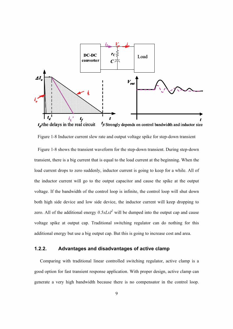
Figure 1-8 Inductor current slew rate and output voltage spike for step-down transient
Figure 1-8 shows the transient waveform for the step-down transient. During step-down
transient, there is a big current that is equal to the load current at the beginning. When the
load current drops to zero suddenly, inductor current is going to keep for a while. All of
the inductor current will go to the output capacitor and cause the spike at the output
voltage. If the bandwidth of the control loop is infinite, the control loop will shut down
both high side device and low side device, the inductor current will keep dropping to
zero. All of the additional energy 0.5xLxI2 will be dumped into the output cap and cause
voltage spike at output cap. Traditional switching regulator can do nothing for this
additional energy but use a big output cap. But this is going to increase cost and area.
1.2.2. Advantages and disadvantages of active clamp
Comparing with traditional linear controlled switching regulator, active clamp is a
good option for fast transient response application. With proper design, active clamp can
generate a very high bandwidth because there is no compensator in the control loop.
10
Since active clamp bypasses inductor and is connected directly to the output cap, it can
fasten source and sink current even during the step-down transient and prevent the
overshooting of the output voltage. This is the biggest advantage for active clamp
comparing with traditional linear control. However, active clamp has a poor efficiency
when the voltage difference between input and output voltage is large. If it is used most
of the time, it is going to affect the efficiency a lot.
1.3. Objective of this work
The objective of this work is to study active clamp concept and use it to improve the
transient response of VRD. In order to do this, existing active clamp structures are
investigated first. Some new concepts like non-linear Gm, error signal feedback etc are
proposed. A non-linear active clamp based on current mirror structure is implemented
using real transistors. A single-phase voltage loop control buck is designed with active
clamp to verify the good transient response performance of the new active clamp
structure.
1.4. Outline of the thesis
The whole thesis is composed of five chapters:
Chapter 1 is the literature review of the background for VRD and the specifications for
VRD10.x. The advantage and disadvantage for traditional switching converter and active
clamp are discussed. Then comes to the objective of this work and outline of the thesis.

11
Chapter 2 is the review of existing active clamp structures from Berkeley and xin’s
structure.
Chapter 3 proposed a new active structure. The details of the new structure are discussed.
Some new concepts are introduced.
Chapter 4 discussed the basic blocks design. Non-linear active clamp implementation,
feedback signal generation, high speed synchronous driver design, single phase voltage
loop control and whole system including active clamp and single phase voltage control
implementation and verification are discussed.
Chapter 5 is the summary of this work.

12
Chapter 2: Review of existing active clamps
2.1. General active clamp structure
Gm
Gm
Vref+ΔV
-ΔVVFB
Vout
Active ClampActive Clamp
Gm
Gm
Vref+ΔV
-ΔVVFB
Vout
Active ClampActive ClampPWM
modulator
driver
CO OP Z1(s)
Z2(s)
Vc
Vin Vout
RS
Q
LX
Compensator
PWM switch L
CR
RC
Vd
Vg
VFB
Linear ControlLinear ControlPWM
modulator
driver
CO OP Z1(s)
Z2(s)
Vc
Vin Vout
RS
Q
LX
Compensator
PWM switch L
CR
RC
Vd
Vg
VFB
PWM modulator
driver
CO OP Z1(s)
Z2(s)
Vc
Vin Vout
RS
Q
LX
Compensator
PWM switch L
CR
RC
Vd
Vg
PWM modulator
driver
CO OP Z1(s)
Z2(s)
Vc
Vin Vout
RS
Q RS
Q
LX
Compensator
PWM switch L
CR
RC
Vd
Vg
VFB
Linear ControlLinear Control
Figure 2-1 General structure for active clamp
Figure 2-1 is general structure for active clamp. The left part in Figure 2-1 is a single-
phase voltage loop controlled buck regulator. A resonant tank consisting of an inductor
and capacitor is included in the output stage. Since inductor current can’t change
dramatically, the output voltage will drop or overshoot during step-up or step-down
transient. The right part is an active clamp structure. There are two paths (pull-up path
and pull-down path) connected directly to the output node. When the feedback voltage
VFB is lower than the low-band reference, a pull up current will be generated and fed into
the output node Vout to rise up output voltage Vout. If the feedback voltage VFB is larger

13
than the high-band reference, a pull down current will be generated and pull down the
output voltage Vout. Since active clamp bypasses the inductor, it can source or sink
current to the output node quickly, which is very good for the fast transient application
like VRD. However, since the efficiency is quite poor for active clamp, it can’ t replace
traditional switching regulator totally to supply the power to the system. Combine the
efficient traditional switching regulator and fast transient active clamp, we can get a
combinational system with a good efficiency at steady state by traditional switching
regulator and fast transient response by active clamp at transient period.
A lot of methods are proposed to speed up the transient response for VRD
application[8] [27]; Figure 2-2 shows the comparison between active clamp and the other
structures. From this figure, we can see that active clamp has the best transient response,
especially for the step-down transient, which enhances the objective of this thesis work.
High switching loss and poor efficiency, poor step-down transient response
High control bandwidth, fast transient response at step-up
High frequency switching regulator
High output ripple, bad transient response at step-down
High bandwidth, fast transient response at step-up
Non-linear controlled switching regulator such as V2 control
High cost and large profileHigh efficiencySwitching regulator with large bulk cap and decoupling cap
Bad efficiency, stability depends on ESR and other parasitic.
Possible high loop bandwidth. Strong pull-up capability good for step up transient, not good for step-down transient
Linear Regulator
Bad efficiency, stability problemHigh bandwidth, fast transient response, especially good for step-down transient response
Active Clamp
DisadvantagesAdvantagesStructures
Figure 2-2 Comparison between active clamp and other fast transient structures
14
A lot of methods are proposed to implement active clamp structure, the topology
described above is the simple bang-bang control. There is a stability problem for this
structure if the band is too narrow and pull-up and pull-down current are too strong. In
this chapter, another two better structures are discussed before the discussion of the new
structure.
2.2. Active clamp structure from Berkeley
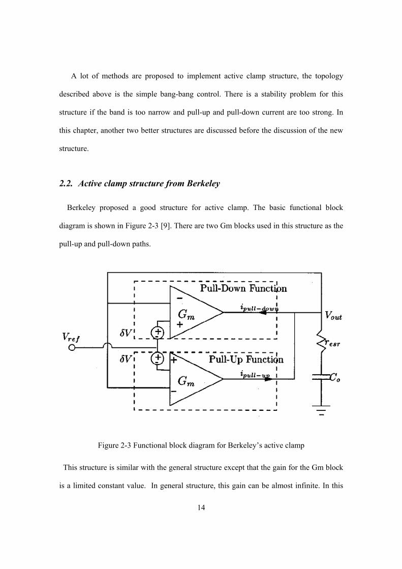
Berkeley proposed a good structure for active clamp. The basic functional block
diagram is shown in Figure 2-3 [9]. There are two Gm blocks used in this structure as the
pull-up and pull-down paths.
Figure 2-3 Functional block diagram for Berkeley’s active clamp
This structure is similar with the general structure except that the gain for the Gm block
is a limited constant value. In general structure, this gain can be almost infinite. In this

15
structure, the Gm block is implemented using a series of current mirrors as shown in
Figure 2-4. A simple differential stage is used as the input stage. Five current-mirror
stages are used as current amplifiers. By doing this, the output current can be accurately
controlled by the gain of those stages. A stable active clamp system can be guaranteed by
tuning the gain of these stages. Since all of the devices are working in the active mode,
the speed of this structure can be very fast. However, the power loss of this structure is
relatively large. If it is triggered most of the time, the total efficiency of the whole system
will drop down dramatically.
Figure 2-4 Schematic of pull-up Gm block
16
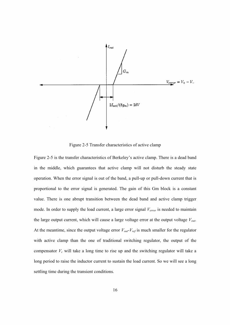
Figure 2-5 Transfer characteristics of active clamp
Figure 2-5 is the transfer characteristics of Berkeley’s active clamp. There is a dead band
in the middle, which guarantees that active clamp will not disturb the steady state
operation. When the error signal is out of the band, a pull-up or pull-down current that is
proportional to the error signal is generated. The gain of this Gm block is a constant
value. There is one abrupt transition between the dead band and active clamp trigger
mode. In order to supply the load current, a large error signal Verror is needed to maintain
the large output current, which will cause a large voltage error at the output voltage Vout.
At the meantime, since the output voltage error Vout-Vref is much smaller for the regulator
with active clamp than the one of traditional switching regulator, the output of the
compensator Vc will take a long time to rise up and the switching regulator will take a
long period to raise the inductor current to sustain the load current. So we will see a long
settling time during the transient conditions.

17
From Figure 2-3, we can see that, three references are needed in the whole system:
one reference for the switching regulator, one low band and one high band for active
clamp. If the dead band is very narrow, three reference voltages that are very close to
each other are needed. It is a little difficult to generate these three references, especially
in switching system like buck. Another shortcoming in this structure is that, there is no
AVP included in this structure. It can’t be used directly for VRD application.
2.3. Transient voltage clamp concept
Reference: xin’s PESC paper “ Impact of Transient voltage clamp on CPU power Delivery” Figure 2-6 Functional block diagram for transient voltage clamp structure
Figure 2-6 is the functional block diagram for transient voltage clamp structure [8].
This structure is more like general structure. Multi-phase buck switching regulator is used
and an AVP structure is implemented in this structure to fit VRD application.

18
2.4. Summary
In this chapter, the general structure for active clamp is reviewed. A comparison
between active clamp and other fast transient response method is done to show the
benefits of active clamp for transient response. Two structures are discussed as good
examples for the existing active clamp topologies.

19
Chapter 3: New active clamp design and modeling
3.1. New active clamp structure
PWM modulator
driver
CO OP Z1(s)
Z2(s)
Vc
Vin Vout
RS
Q
LX
Compensator
PWM switch L
CR
RC
Vd
Vg
VFB_l
Linear ControlLinear Control
RLL∗ILoad
PWM modulator
driver
CO OP Z1(s)
Z2(s)
Vc
Vin Vout
RS
Q RS
Q
LX
Compensator
PWM switch L
CR
RC
Vd
Vg
VFB_l
Linear ControlLinear Control
RLL∗ILoad
AsGm
AsGm
Vref
VFB
Iout
New Active ClampNew Active Clamp
RLL∗ ILoad
Vout1/N
Ierror
V-
V+
V+
V-
AsGm
AsGm
Vref
VFB
Iout
New Active ClampNew Active Clamp
RLL∗ ILoad
Vout1/N
Ierror
V-
V+
V+
V-
Figure 3-1 Structure of new active clamp with linear voltage control loop
From the discussion in chapter 2, we can see that there are some shortcomings for the
existing active clamp structures. A new active clamp structure is proposed in this chapter.
The functional block diagram of this new active clamp is shown in Figure 3-1. The left
side of this figure is the same single-phase buck regulator with AVP. The right part is the
new active clamp.

20
AsGm
AsGm
Vref
VFB
Iout
New Active ClampNew Active Clamp
RLL∗ ILoad
Vout
1/N Ierror
V-
V+
V+AsGm
AsGm
Vref
VFB
Iout
New Active ClampNew Active Clamp
RLL∗ ILoad
Vout
1/N Ierror
V-
V+
V+
Figure 3-2 Structure of new active clamp
The new active clamp structure is redrawn in Figure 3-2 for the analysis purpose. There
are two outputs from this new active clamp, one is the output to load Iout, and the other
output is the error signal feedback Ierror to generate a larger error signal for linear control
loop. The error signal feedback gain can’t be too high for the stability issue. Only one
reference is needed in this new active clamp since two asymmetric Gm blocks with built-
in offset are used as the pull-up and pull-down paths. This approach simplifies the active
clamp design a lot. Two fully differential input stages are used in these asymmetric Gm
blocks to improve the matching accuracy and common mode rejection ratio (CMRR).
AVP is included in this new structure as the left part. A load line resistor RLL is used to
generate a voltage difference between Vout and VFB. The current source in the picture is
the current sensor output. It is used to generate a voltage difference across the resistor
that is proportional to the load current.

21
Ref VFb0.9Ref 1.1Ref
Iout
Ref VFb0.9Ref 1.1RefRef VFb0.9Ref 1.1Ref
Iout
S1
S2
S3
S1
S2
S3Dead band
Step up Step down
Dead band
Step up Step down
Figure 3-3 Transfer characteristics for the new active clamp
If we consider the transfer characteristics between VFB and Iout, it is going to be a non-
linear curve shown in Figure 3-3. Comparing it with the transfer characteristics of
Berkeley’s active clamp structure shown in Figure 2-5, we will see that, the slope of this
curve is different at different voltage error VFB-VREF. There is a dead band around the
reference voltage too. When output voltage error VFB-VREF is out of the dead band, a
current Iout will be generated. If the error signal VFB-VREF is small, a small current will be
generated. When the error signal is bigger and bigger, the gain between the voltage error
VFB-VREF and output current Iout will rise up and finally goes to infinite. Gm block will
source or sink enough current to prevent the output voltage from rising or falling. When

22
the output voltage error is reduced, the gain between the voltage error VFB-VREF is
reduced too and finally goes to zero at steady state. By using this non-linear Gm block, a
smooth transition between dead band and active clamp triggering mode is generated. At
the mean time, this control provides a smooth transition between traditional linear control
and bang-bang control. The output voltage error will be guaranteed in the window of
these two saturation error voltages. By choosing proper value of the slopes, a stable
system can be guaranteed. Combine this new active clamp structure and traditional linear
control, we can get a good efficiency at steady state because of the traditional linear
control and a good transient response during transient period due to this new active
clamp.
3.2. Comparison between new active clamp structure and other structures
Ref VFb0.9Ref 1.1Ref
Iout
Ref VFb0.9Ref 1.1RefRef VFb0.9Ref 1.1Ref
Iout
Linear controlLinear control
Figure 3-4 Transfer characteristics for linear control

23
In this section, we will do a comparison between the new active clamp structure and
the other control methods. Figure 3-3 shows the transfer characteristics of this new active
clamp structure. In original linear control, there is no other gain directly connected to the
output voltage node Vout, so the equivalent transfer characteristics for linear control in
this transfer characteristics plane is X-axis shown in Figure 3-4.
Ref VFb0.9Ref 1.1Ref
Iout
Ref VFb0.9Ref 1.1RefRef VFb0.9Ref 1.1Ref
Iout
Traditional bang-bang control
Traditional bang-bang control
Figure 3-5 Transfer characteristics for bang-bang controlled active clamp
Figure 3-5 shows the transfer characteristics for traditional non-linear controlled active
clamp ⎯ bang-bang control. Equivalently, bang-bang control is a segmented Y-axis. As
mentioned before, linear control looks like an X-axis. We can see that new active clamp
structure make a very smooth transition from linear control to an infinite gain bang-bang

24
control. New active clamp structure keeps the high steady-state performance of linear
control; meanwhile generates the fast transient response of bang-bang control. New
active clamp structure exactly fits the ideal control concept proposed in[23]!
Ref VFb0.9Ref 1.1Ref
Iout
Ref VFb0.9Ref 1.1RefRef VFb0.9Ref 1.1Ref
Iout
BerkeleyBerkeley
Figure 3-6 Transfer characteristics of Berkeley’s active clamp structure
Figure 3-6 shows the transfer characteristics of Berkeley’s active clamp structure. There
is a dead band in the middle, which guarantees that active clamp will not disturb the
steady state. When the error signal is out of the band, a pull-up or pull-down current that
is proportional to the error signal is generated. The gain of this Gm block is a constant
value. There is one abrupt transition between the dead band and active clamp trigger
mode. In order to saturate the load current, a large error signal is needed to maintain the
large load current, which will cause a large voltage error at the output voltage. At the
meantime, since the output voltage error is much smaller comparing with traditional

25
switching regulator, the output of the compensator will take a long time to rise up and
switching regulator will take a long time to raise the inductor current to sustain the load
current. So we will see a long settling time during the transient conditions. In the new
active structure, most of the shortcomings are overcome by the non-linear Gm and error
signal feedback.
3.3. AVP implementation
iO
ΔIO
VBulk
ΔVo
VBulk
ΔVo
VrefVFB
VrefVFBVFB
ILIL
RLL∗ILoadRLL∗ILoad
Figure 3-7 AVP implementation in new active clamp structure

26
In order to reduce voltage spike during the transient, Intel proposed AVP concept,
which means that, the output voltage will be lower at heavy load and higher at light load.
By using AVP concept, the output voltage spike will be reduced almost 50%. AVP is a
built-in part for VRD application [10]. In this new active clamp structure, AVP is
implemented as shown in Figure 3-2. As shown in Figure 3-7, before the load Io changes,
the output voltage is very close to the reference voltage. When load current Io rise to a
new level, a voltage difference will generate across the resistor in Figure 3-2. This
voltage difference is proportional to the load current and the value is RLLxILoad. After the
load step up, the output voltage is going to be Vref - RLLxILoad, which is lower than
reference voltage. At step down, the output voltage is going to go back the reference
voltage. By using AVP, the output voltage can be reduced almost 50% as shown in
Figure 3-8.
ΔVstep-downVmax
Vmin
W/O AVP
iO
Vmax
Vmin
W/ AVP ΔVstep-down
ΔVstep-downVmax
Vmin
W/O AVP
iO
ΔVstep-downVmax
Vmin
W/O AVP
iO
Vmax
Vmin
W/O AVP
iO
Vmax
Vmin
W/ AVP ΔVstep-downVmax
Vmin
W/ AVP ΔVstep-down
Figure 3-8 AVP reduce the total voltage spike

27
3.4. Error feedback concept
As mentioned before, if active clamp is used during transient period, there will be a
longer settling time because of the small error signal in the compensator. Figure 3-9
shows the transient waveform for normal linear control. When the load current steps up,
the output voltage will drop down because the unbalance between the inductor current
and the output current. There will be a voltage difference between Vref and VFB. In normal
linear control, this error signal can be relatively large. This large error signal will rise up
the control signal Vc quickly to generate larger duty cycle. The inductor current will rise
up quickly to sustain the load current. When inductor current is equal to the load current,
output voltage will not drop down anymore.
iO
Vc
ΔIO
Vref
VFB
IL
VBulkΔVo
VBulkΔVo
VBulkΔVo
Figure 3-9 Transient waveform for linear control
28
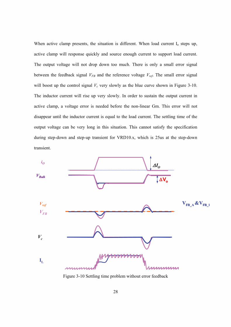
When active clamp presents, the situation is different. When load current Io steps up,
active clamp will response quickly and source enough current to support load current.
The output voltage will not drop down too much. There is only a small error signal
between the feedback signal VFB and the reference voltage Vref. The small error signal
will boost up the control signal Vc very slowly as the blue curve shown in Figure 3-10.
The inductor current will rise up very slowly. In order to sustain the output current in
active clamp, a voltage error is needed before the non-linear Gm. This error will not
disappear until the inductor current is equal to the load current. The settling time of the
output voltage can be very long in this situation. This cannot satisfy the specification
during step-down and step-up transient for VRD10.x, which is 25us at the step-down
transient.
iO
Vc
ΔIO
Vref
VFB
IL
VFB_A &VFB_lVFB_A &VFB_l
VBulkΔVo
VBulkΔVo
VBulkΔVo
Figure 3-10 Settling time problem without error feedback
29
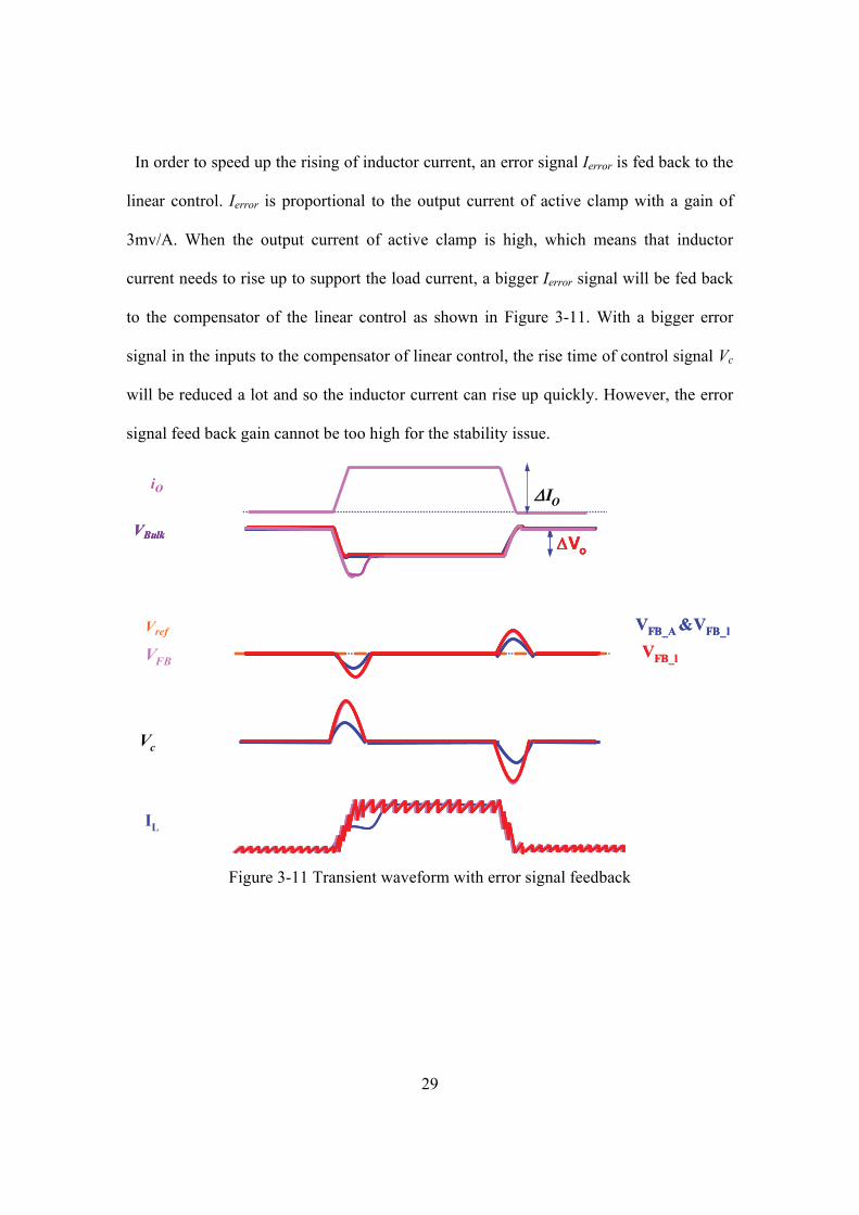
In order to speed up the rising of inductor current, an error signal Ierror is fed back to the
linear control. Ierror is proportional to the output current of active clamp with a gain of
3mv/A. When the output current of active clamp is high, which means that inductor
current needs to rise up to support the load current, a bigger Ierror signal will be fed back
to the compensator of the linear control as shown in Figure 3-11. With a bigger error
signal in the inputs to the compensator of linear control, the rise time of control signal Vc
will be reduced a lot and so the inductor current can rise up quickly. However, the error
signal feed back gain cannot be too high for the stability issue.
iO
Vc
ΔIO
Vref
VFB
IL
VFB_A &VFB_lVFB_A &VFB_l
VFB_lVFB_l
VBulkΔVo
VBulkΔVo
VBulkΔVo
Figure 3-11 Transient waveform with error signal feedback

30
3.5. Summary
In this chapter, a new active clamp structure is proposed and discussed in details. Non-
linear Gm is used for this new structure. Comparing with existing active clamp structure,
new active clamp structure has a better transient response, smaller settling down time and
simpler structure.
31
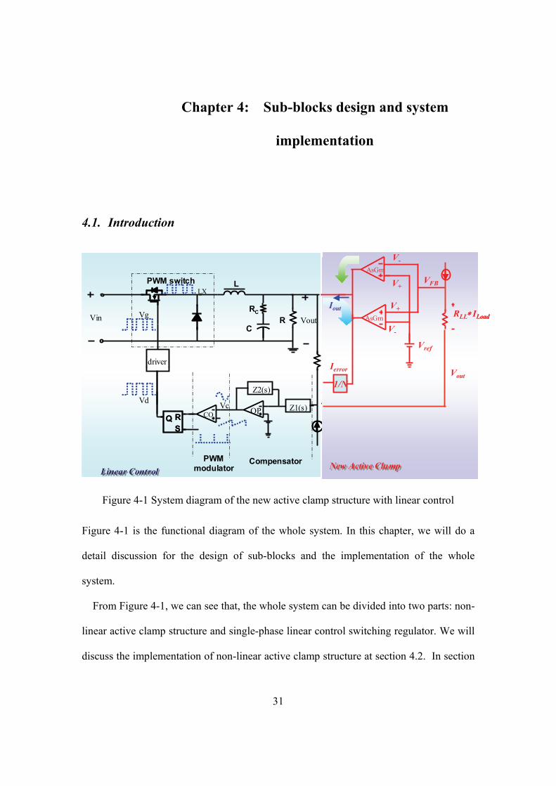
Chapter 4: Sub-blocks design and system
implementation
4.1. Introduction
PWM modulator
driver
CO OP Z1(s)
Z2(s)
Vc
Vin Vout
RS
Q
LX
Compensator
PWM switch L
CR
RC
Vd
Vg
VFB_l
Linear ControlLinear Control
RLL∗ILoad
PWM modulator
driver
CO OP Z1(s)
Z2(s)
Vc
Vin Vout
RS
Q RS
Q
LX
Compensator
PWM switch L
CR
RC
Vd
Vg
VFB_l
Linear ControlLinear Control
RLL∗ILoad
AsGm
AsGm
Vref
VFB
Iout
New Active ClampNew Active Clamp
RLL∗ ILoad
Vout1/N
Ierror
V-
V+
V+
V-
AsGm
AsGm
Vref
VFB
Iout
New Active ClampNew Active Clamp
RLL∗ ILoad
Vout1/N
Ierror
V-
V+
V+
V-
Figure 4-1 System diagram of the new active clamp structure with linear control
Figure 4-1 is the functional diagram of the whole system. In this chapter, we will do a
detail discussion for the design of sub-blocks and the implementation of the whole
system.
From Figure 4-1, we can see that, the whole system can be divided into two parts: non-
linear active clamp structure and single-phase linear control switching regulator. We will
discuss the implementation of non-linear active clamp structure at section 4.2. In section

32
4.3, 4.4 and 4.5, we are going to discuss the design of single-phase voltage control
switching converter. In 4.6, we are going to discuss the whole system implementation and
verification.
4.2. Non-linear Active Clamp Design
AsGm
AsGm
Vref
VFB
Iout
New Active ClampNew Active Clamp
RLL∗ ILoad
Vout
1/N Ierror
V-
V+
V+AsGm
AsGm
Vref
VFB
Iout
New Active ClampNew Active Clamp
RLL∗ ILoad
Vout
1/N Ierror
V-
V+
V+
Figure 4-2 New active clamp structure
Figure 4-2 is the new active clamp structure. The core part of this structure is the non-
linear asymmetric Gm block. We are going to discuss the implementation of the non-
linear asymmetric Gm blocks in this section.

33
4.2.1. Asymmetric Gm block with built-in offset design
V+- V-
IoutGmIout
Ib
V+ V-
V+- V-
IoutGmIout
Ib
V+ V-
V+- V-
Iout
V+- V-
IoutGmIout
Ib
V+ V-
GmIout
Ib
V+ V-
Figure 4-3 Symmetric Gm block
Figure 4-3 is a two-stage symmetric Gm block [11] [12]. The first stage of this Gm block
is a fully differential low gain pre-amplifier. By using large input devices, a good offset
and CMRR can be guaranteed. The fully differential output signals will be fed into a Gm
block to generate a current Iout. The transfer characteristic of this symmetric Gm block is
shown in the right figure in Figure 4-3. When error signal |V+-V-| is zero, there is a big
gain in this transfer function. It is not what we need for the new non-linear active clamp.
In order to generate a zero gain in the transfer function, we need to do some change for
this symmetric structure. From Figure 4-3, we can see that the gain of this transfer
characteristics is zero at large |V+-V-|. If we can use this point as the steady state point, we
will get the transfer characters with a gain zero at steady state. For this purpose, a new
structure is developed in Figure 4-4.

34
GmIout
Ib
V+ V-
V+- V-
IoutGmIout
Ib
V+ V-
GmIout
Ib
V+ V-
V+- V-
Iout
V+- V-
Iout
Figure 4-4 Asymmetric Gm block
In the asymmetric Gm block shown in Figure 4-4, the input devices are not balanced. A
bigger device is used at the negative input terminal. When the differential signal at the
input terminals is zero, there is a current at the output. By choosing the correct device
value, the transfer characteristics curve can be shift to the right plane as shown in the
right figure in Figure 4-4. Now, we got a curve with zero gain when the error signal |V+-
V-| is zero. However, there is a DC current at the output when the error signal |V+-V-| is
zero. In the discussion before, we said that we don’t want active clamp to disturb the
steady state operation, which means that the value for the output current should be zero
and the gain of the transfer characteristics should be zero too. This curve is not exactly
what we want. From Figure 4-4, we can see that, if the curve is shifted up along Y-axis,
we will get a curve with zero DC value and zero gain at steady state. That is exactly what
we want! For this purpose, another new structure is developed in Figure 4-5.

35
V+- V-
IoutGm
Iout
Ib
V+ V-
Ioffset
V+- V-
Iout
V+- V-
IoutGm
Iout
Ib
V+ V-
Ioffset
GmIout
Ib
V+ V-
Ioffset
Figure 4-5 Asymmetric Gm block with Ioffset
In Figure 4-5, an offset current Ioffset is added to the output of this Gm block to shift the
curve up along y-axis. Now, we got a curve with a zero value and zero gain at steady
state. When error signal |V+-V-| goes up, Iout will smoothly along a two-order curve and
finally saturate at a high level.

36
4.2.2. Non-linear Gm block design
V-Comp
Iout
Isat
V+
GmIout
Ib
V+ V-
Ioffset
GmIout
Ib
V+ V-
Ioffset
GmIout
Ib
V+ V-
Ioffset
GmIout
Ib
V+ V-
Ioffset
Iout_tot
V-Comp
Iout
Isat
V+
GmIout
Ib
V+ V-
Ioffset
GmIout
Ib
V+ V-
Ioffset
GmIout
Ib
V+ V-
Ioffset
GmIout
Ib
V+ V-
Ioffset
Iout_tot
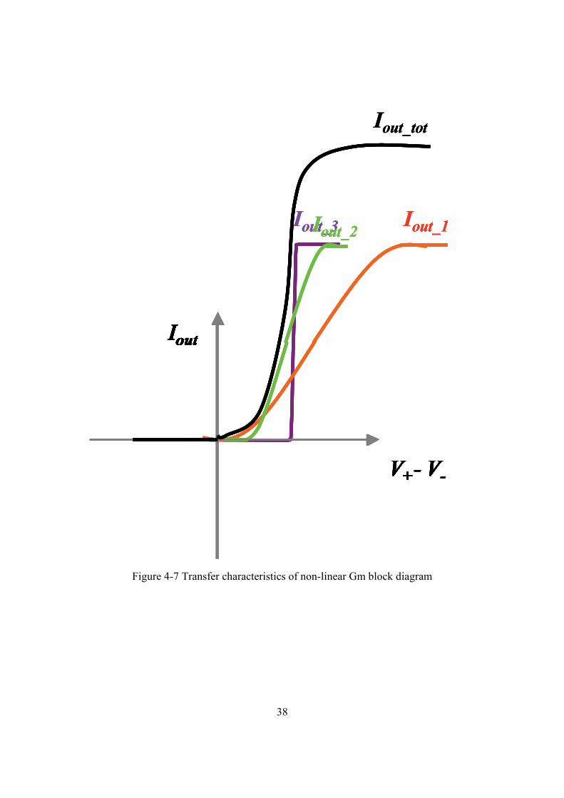
Figure 4-6 Non-linear Gm block diagram
By using this asymmetric Gm block with built-in offset shown in Figure 4-5, we can
generate a two-order non-linear current. However, this curve is still different from the
curve shown in Figure 3-3 since it needs a large error signal |V+-V-| to saturate the output
current Iout. However, the tolerance band of VRD is very small, we need transfer function

37
with a small saturation error signal. From Figure 3-3, we can see that, at lower |V+-V-|,
the slope is small, at higher |V+-V-|, the slope is higher. If we can use a small slope
transfer function at low |V+-V-|, and a large slope transfer function at high |V+-V-|, we can
solve this problem. For this purpose, a new structure is designed as shown in Figure 4-6.
In this structure, three currents are generated and summed together to get a sharp non-
linear transfer function. The transfer function is shown in Figure 4-7. Iout_1 is generated
using a source degenerated differential pre-amplifier. The slew rate is small. It is
dominant at low V+-V- part. Iout_2 is generated using a general differential pre-amplifier. The
slew rate of Iout_2 is large. It is dominant at medium V+-V- part. Iout_3 is generated using a
comparator. Slew rate is almost infinite. It is used to saturate active clamp current at high
V+-V- part. Summing them together, a sharp non-linear transfer function Iout_tot is achieved.
This transfer function has the same feature as the one shown in Figure 3-3. By using this
structure, we got the exact transfer function we want!
38
V+- V-
Iout
Iout_3
V+- V-
Iout
Iout_1
V+- V-
Iout
Iout_2
V+- V-
Iout
Iout_tot
V+- V-
Iout
Iout_3
V+- V-
Iout
V+- V-
Iout
Iout_3
V+- V-
Iout
Iout_1
V+- V-
Iout
V+- V-
Iout
Iout_1
V+- V-
Iout
Iout_2
V+- V-
Iout
V+- V-
Iout
Iout_2
V+- V-
Iout
Iout_tot
V+- V-
Iout
V+- V-
Iout
Iout_tot
Figure 4-7 Transfer characteristics of non-linear Gm block diagram

39
4.2.3. Non-linear active clamp based on current mirrors
V-Comp
Iout
Isat
V+
GmIout
Ib
V+ V-
Ioffset
GmIout
Ib
V+ V-
Ioffset
GmIout
Ib
V+ V-
Ioffset
GmIout
Ib
V+ V-
Ioffset
Iout_tot
V-Comp
Iout
Isat
V+
GmIout
Ib
V+ V-
Ioffset
GmIout
Ib
V+ V-
Ioffset
GmIout
Ib
V+ V-
Ioffset
GmIout
Ib
V+ V-
Ioffset
Iout_tot
CurrentMirror x10
CurrentMirror x10
CurrentMirror x10
CurrentMirror x10
CurrentMirror x10
PGND PGND
PVDD PVDD PVDD
Vout
CurrentMirror x10
CurrentMirror x10
CurrentMirror x10
CurrentMirror x10
CurrentMirror x10
PGND PGND
PVDD PVDD PVDD
Vout
Ierror_fbIerror_fb
Figure 4-8 Non-linear active clamp block diagram (pull-up path)
In 4.2.2, we got the transfer function by using structure shown in Figure 4-6. However,
this current is too small to drive the output node. We need to amplify this current signal.
A current mirror based structure is developed as shown in Figure 4-8. The current Iout_tot
is amplified to a higher level like 30A to drive the system output node Vout as shown in
Figure 4-1. Figure 4-8 shows only the pull-up path, the pull-down path has similar
structure like the pull-up path.
40
4.2.4. Final Schematic and simulation results
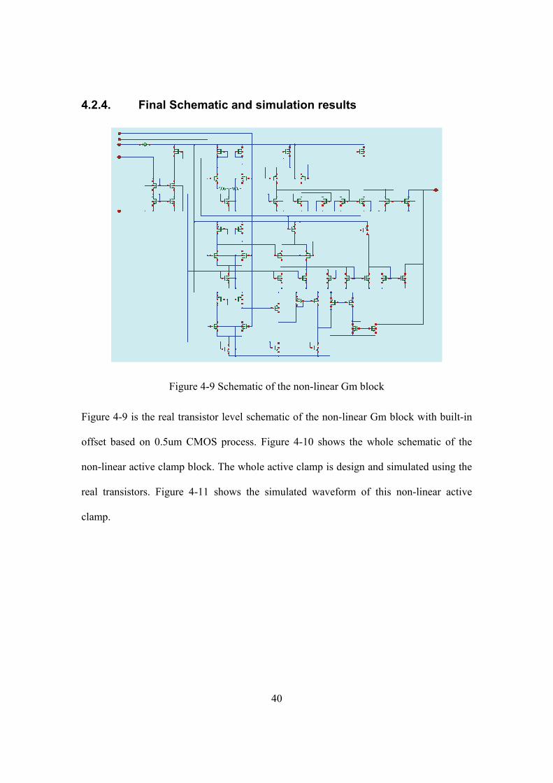
Figure 4-9 Schematic of the non-linear Gm block
Figure 4-9 is the real transistor level schematic of the non-linear Gm block with built-in
offset based on 0.5um CMOS process. Figure 4-10 shows the whole schematic of the
non-linear active clamp block. The whole active clamp is design and simulated using the
real transistors. Figure 4-11 shows the simulated waveform of this non-linear active
clamp.

41
Figure 4-10 Schematic of the whole non-linear active clamp block
Transfer characteristics of non-linear active clamp
-30
-20
-10
0
10
20
30
-0.050 -0.030 -0.010 0.010 0.030 0.050
Vref-VFB
Iout
(A)
Figure 4-11 Simulated transfer characteristics of non-linear active clamp

42
4.2.5. Summary
A non-linear active clamp structure is implemented in this part using real transistors
based on 0.5um CMOS process. The implementation of non-linear Gm block with built-
in offset is discussed in details. The whole non-linear Gm block is designed using real
transistor and verified by spice simulation.

43
4.3. AVP, Error Signal Feedback implementation
RLL∗ ILoad
SRNCurSen
SRP
CurrentMirror x1
VDD
RLL∗ Iload+Verror_fb
Vout
Ierror_fb
VFB_A
VFB_LRLL∗ ILoad
SRNCurSen
SRP
CurrentMirror x1
VDD
RLL∗ Iload+Verror_fb
Vout
Ierror_fb
VFB_A
VFB_L
Figure 4-12 Feed back signal generation block
AVP and error signal feedback are implemented in feed back signal generation block
[13]. Figure 4-12 is the block diagram of feedback signal generation block. SRP and SRN
are the sensing input points to the current sensor. The output of current sensor is mirrored
to another two current sources. One of them is used to generate feedback signal for active
clamp VFB_A, the other is used to generate the feedback signal for linear control loop
VFB_L. There is a resistor on both feedback signal generation paths. In VFB_A path, the
voltage difference on the resistor is RLL*ILoad, which will generate AVP function. In VFB_L
path, the voltage difference on the resistor is RLL*ILoad+Verror_fb, which will generate AVP
44
function and error feedback function. By using this structure, we can realize AVP and
error signal feedback function at the same time.
4.4. High speed synchronous driver design
SR
QSR
Q
LevelshifterLevelshifter Cboo
t
low sidedriver
high sidedriver
S
R
Low side gate sensor
High side gate sensor
+-+- +
-+-
Vref
Compensator
Vc
ramp
clock
D
rising edge pulse
comparator
Vdror
Vcc
Vpower in
Vout
NOR
AND
Synchronous driver
PWM_IN
Figure 4-13 Synchronous driver in a single-phase buck converter
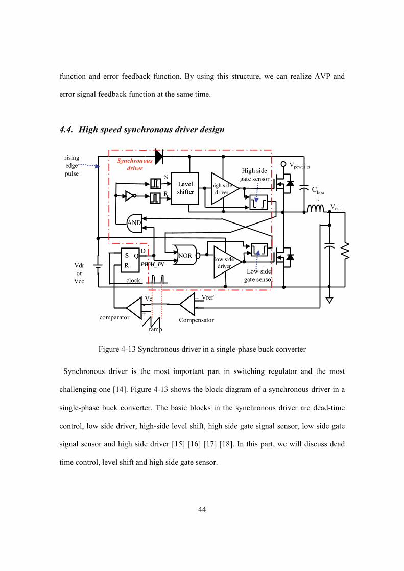
Synchronous driver is the most important part in switching regulator and the most
challenging one [14]. Figure 4-13 shows the block diagram of a synchronous driver in a
single-phase buck converter. The basic blocks in the synchronous driver are dead-time
control, low side driver, high-side level shift, high side gate signal sensor, low side gate
signal sensor and high side driver [15] [16] [17] [18]. In this part, we will discuss dead
time control, level shift and high side gate sensor.

45
4.4.1. Dead-time control
As shown in Figure 4-13, a break-before-make logic is used in the circuit design. The
objective of the dead-time control is to prevent shoot rough with a minimum dead time.
When PWM_IN signal goes high, it will turn off the low side device first. When low side
gate signal goes to low, low side gate sensor signal will go to high and enable the high
side switch. The PWM_IN signal will pass through the AND gate to the high side level
shift circuit. The logic signal will be level shifted to high side gate driver and turn on the
high side device. When PWM_IN signal goes to low, it will turn off the high side device
first. High side gate sensor signal will go to low and enable the low side switch.
PWM_IN signal will pass through the NOR gate and turn on the low side switch. By
using this break-before-make logic, the high side and low side device will not be turned
on at the same time and cause the shoot through problem. This dead time control scheme
is so-called adaptive dead time control. The minimum dead time to be achieved is
determined by the delay of the high side driver, low side driver and gate signal sensors. In
this drive design, the minimum dead time can be around 10ns by using 0.5um CMOS
process.
46
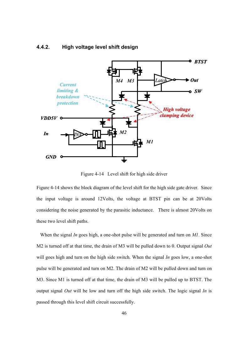
4.4.2. High voltage level shift design
High voltage clamping device
Current limiting & breakdown protection
Latch
INVIn
Out
BTST
SW
GND
VDD5V
High voltage clamping device
High voltage clamping device
Current limiting & breakdown protection
Current limiting & breakdown protection
Latch
INVIn
Out
BTST
SW
GND
VDD5V
M1
M2
M3M4
Figure 4-14 Level shift for high side driver
Figure 4-14 shows the block diagram of the level shift for the high side gate driver. Since
the input voltage is around 12Volts, the voltage at BTST pin can be at 20Volts
considering the noise generated by the parasitic inductance. There is almost 20Volts on
these two level shift paths.
When the signal In goes high, a one-shot pulse will be generated and turn on M1. Since
M2 is turned off at that time, the drain of M3 will be pulled down to 0. Output signal Out
will goes high and turn on the high side switch. When the signal In goes low, a one-shot
pulse will be generated and turn on M2. The drain of M2 will be pulled down and turn on
M3. Since M1 is turned off at that time, the drain of M3 will be pulled up to BTST. The
output signal Out will be low and turn off the high side switch. The logic signal In is
passed through this level shift circuit successfully.

47
There are four high voltage diodes used in this circuit to clamp the nodes so that the low
voltage device at the low side and high side will not be breakdown. These two resistors
are used as current limiting device to prevent high current spike. All of the high side
devices are placed in an isolated tub. The ground of these devices is the switching node
and the power supply is the bootstrap node BTST.
4.4.3. High side gate signal sensor design
As we discussed above, the low side logic signal needs to be level shifted to high side.
The high side logic signal needs be level shifted down to low side too. A level shift down
circuit is a mirror of the level shift up circuit shown in Figure 4-14. The detail circuit is
shown in the final schematic shown in Figure 4-15.

48
4.4.4. High-speed synchronous driver design
High side driverHigh side driverLatchLatch
Low side driverLow side driver
Level shift
High side gate sensorHigh side
gate sensor
Low side gate sensor
Low side gate sensor
Figure 4-15 Final schematic for the synchronous driver
Figure 4-15 is the final schematic for the synchronous driver. It consists of low side gate
sensor, high side gate sensor, low side driver, high side driver and high side level shift.
Figure 4-16 is the simulated timing diagram for the synchronous driver. From the
waveform, we can see that the dead time is around 13ns.

49
12ns12ns 13ns
Figure 4-16 Simulated time diagram for synchronous driver
50
4.5. Single channel voltage loop design
PWM modulator
driver
CO OP Z1(s)
Z2(s)
Vc
Vin Vout
RS
Q
LX
Compensator
PWM switch L
CR
RC
Vd
Vg
VFB_l
Linear ControlLinear Control
RLL∗ ILoad
PWM modulator
driver
CO OP Z1(s)
Z2(s)
Vc
Vin Vout
RS
Q RS
Q
LX
Compensator
PWM switch L
CR
RC
Vd
Vg
VFB_l
Linear ControlLinear Control
RLL∗ ILoad
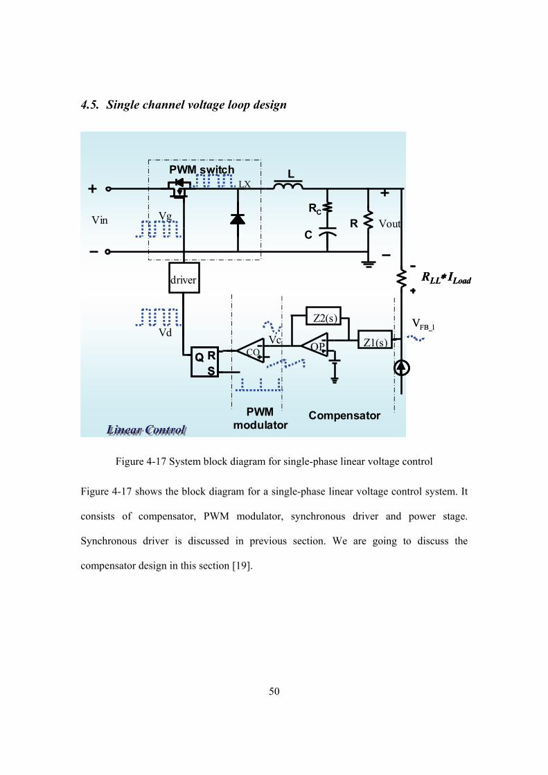
Figure 4-17 System block diagram for single-phase linear voltage control
Figure 4-17 shows the block diagram for a single-phase linear voltage control system. It
consists of compensator, PWM modulator, synchronous driver and power stage.
Synchronous driver is discussed in previous section. We are going to discuss the
compensator design in this section [19].

51
Table 4-1 Specification of the single-phase buck
1MHzFsw
0.8uHL20AIo1nHESL5mOhmESR4X270uF SP CapCo1VVout12VVin
1MHzFsw
0.8uHL20AIo1nHESL5mOhmESR4X270uF SP CapCo1VVout12VVin
Table 4-1 shows the specifications the experimental single-phase buck converter. A high
frequency 1MHz switching regulator is chosen as the linear control switching converter
in the final system.
4.5.1. Loop compensation design
Type III compensator
Figure 4-18 Compensator used in the linear controlled single-phase buck
52
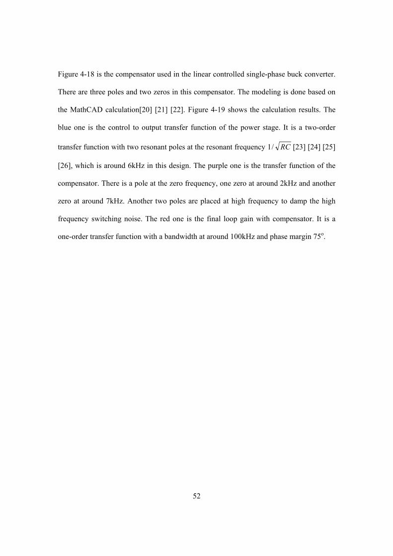
Figure 4-18 is the compensator used in the linear controlled single-phase buck converter.
There are three poles and two zeros in this compensator. The modeling is done based on
the MathCAD calculation[20] [21] [22]. Figure 4-19 shows the calculation results. The
blue one is the control to output transfer function of the power stage. It is a two-order
transfer function with two resonant poles at the resonant frequency RC/1 [23] [24] [25]
[26], which is around 6kHz in this design. The purple one is the transfer function of the
compensator. There is a pole at the zero frequency, one zero at around 2kHz and another
zero at around 7kHz. Another two poles are placed at high frequency to damp the high
frequency switching noise. The red one is the final loop gain with compensator. It is a
one-order transfer function with a bandwidth at around 100kHz and phase margin 75o.

53
10 100 1 .103 1 .104 1 .105 1 .106 1 .10720
8.89
2.22
13.33
24.44
35.56
46.67
57.78
68.89
8080
20−
gain T 2i π⋅ f n⋅( )( )
gain G vc 2i π⋅ f n⋅( )( )
gain A 2i π⋅ f n⋅( )( )
1 107⋅10 f n
10 100 1 .103 1 .104 1 .105 1 .106 1 .107180
156
132
108
84
60
36
12
12
36
6060
180−
phase T 2i π⋅ f n⋅( )( )
phase G vc 2i π⋅ f n⋅( )( )
phase A 2i π⋅ f n⋅( )( )
10710 f n
T
Fm*Gvd
A
Figure 4-19 Compensation design based on MathCAD

54
4.5.2. Schematic and verification
Figure 4-20 Final schematic for the single-phase voltage control buck
Figure 4-20 shows the final schematic for the single-phase voltage controlled buck. All of
the blocks are based on real transistors. Figure 4-21 shows the simulated waveform for
the single-phase voltage controlled buck. There is a big over shoot voltage at the step
down, which is caused by the additional energy in the inductor during the step down. The
linear control can do nothing for this even by shutting down both power switches. There
is a voltage drop at the step-up transient too. The settling down time is small due to the
large error signal between VFB and VBULK.

55
VFBVREF VBULK
IL
Big overshoot at step down!!!
Additional energy in inductor will all be all dumped into
output cap!
Figure 4-21 Simulated waveform for single-phase voltage control buck without active
clamp

56
4.6. System implementation and verification
Figure 4-22 The final test bench for the whole system
By combining the active clamp and linear control buck switching converter, we got the
final system with both linear control loop for steady state and active clamp function for
fast transient response. Figure 4-22 shows the final test bench. SPECACP_R1 is the final
system with both active clamp and linear control buck. The full power delivery path with
four loops is used in the simulation to check the performance of the transient response.

57
tsettsettset
< 12mV< 12mV
< 10mV< 10mV
Figure 4-23 Transient response with both linear control loop and active clamp
Figure 4-23 is the transient response waveform with both linear control loop and active
clamp. From the figure, we can see that the active clamp is triggered at both step-up and
step-down transient. The big voltage spike at the step-down transient disappears because
that active clamp sinks most of the additional current in inductor during step down
transient. This is the biggest benefit achieved by active clamp. At step-up, the voltage
drop is smaller that the one with only linear control loop. The tsettle_down time in this
simulation is around 40us, which is larger than 25us, but the output voltage is already in
the tolerance band. It can still satisfy the step-down specification. From the simulation,
we can see that the transient response performance with both linear control and active
control is very good. It is going to be a good solution for the fast transient response for
VRD application.

58
Linear control with Co=4X270uF SP Cap
Linear control with Co=8X270uF SP Cap
Linear control + active clamp Co=4X270uF SP Cap
Linear control + active clamp Co=8X270uF SP Cap
Figure 4-24 Transient response with and without active clamp for different bulk cap
Figure 4-24 is another transient response waveform with and without active clamp for
different bulk cap. From the simulation results, we can see that the transient response
performance with active clamp is not sensitive to the bulk cap size. However, the
performance with only linear control loop is quite sensitive to bulk cap size. So the bulk
cap can be reduced with active clamp. This is another benefit for active clamp.
4.7. Summary
In this chapter, the implementation of asymmetric non-linear Gm block with built-in
offset is discussed first. The non-linear active clamp design, synchronous driver design

59
and single-phase voltage control design are discussed. Finally, the design and verification
of the whole system are discussed.

60
Chapter 5: Summary and future work
5.1. Summary
In this work, a new active clamp structure is proposed for VRD application. Comparing
with the existing active clamp structure, the new active clamp structure has the following
benefits:
Accurate current control using current mirrors
Dead band used to keep active clamp from steady state operation
Non-linear Gm to guarantee smooth transition between linear control, active
clamp and bang-bang control
Error signal feedback to reduce settling time
Share the same reference with linear control by using asymmetric Gm block
with built-in offset, which simplifies final circuit design
AVP is included
Fully differential input stage, low offset and better CMRR
This new non-linear active clamp structure is implemented using asymmetric Gm block
with built-in offset voltage. The whole active clamp structure is implemented using the
real transistor based on 0.5um CMOS process. A combinational system with a single-
phase linear controlled buck converter and the new active clamp structure is developed
and verified to demonstrate the fast transient response performance of the new active
clamp structure.

61
5.2. Future work
The following are some future works that are good for this research work:
Multi-phase system with active clamp
Fabricate experimental chip

62
References
[1] Intel Corporation, “ Voltage Regulator-Down (VRD) design guide”, Apr 2003,
available on www.Intel.com
[2] Intel Corporation, “ Intel Pentium 4 Processor in the 423 pin package / Intel 850
chipset platform design guide”, Feb 2002, available on www.Intel.com
[3] Yuancheng Ren, Kaiwei Yao, Ming Xu and Fred C. Lee, “Analysis of the Power
Delivery Path from the 12V VR to the Microprocessor”, IEEE APEC 2004
[4] Ed Stanford, “Intel technology VR road map,” Intel Power Supply Technology
Symposium, Sept. 2001.
[5] Kaiwei Yao, Yu Meng, Peng Xu and Fred C. Lee, “Design Considerations for VRM
Transient Response Based on the Output Impedance,” Applied Power Electronics
Conference and Exposition, 2002. APEC 2002. Seventeenth Annual IEEE , Volume:
1 , 10-14 March 2002, Page(s): 14 -20.
[6] Pit-Leong Wong, Fred C. Lee, Xunwei Zhou and Jiabin Chen, “VRM Transient Study
and Output Filter Design for Future Processor,” Industrial Electronics Society, 1998.
IECON '98. Proceedings of the 24th Annual Conference of the IEEE , Volume: 1 , 31
Aug.-4 Sept. 1998, Page(s): 410 -415.
[7] P.L. Wong, “Performance improvements of multi-channel interleaving voltage
regulator modules with integrated coupling inductors,” Dissertation of Virginia
Polytechnic Institute and State University, March 2001.

63
[8] Xin zhang, Alex Huang, “Impacts of Transient Voltage Clamp on CPU Power
Delivery”, IEEE PESC 2004
[9] Albert M. Wu and Seth R. Sanders, “An Active Clamp Circuit for Voltage Regulation
Module (VRM) Applications,” Power Electronics, IEEE Transactions on , Volume: 16
Issue: 5 , Sept. 2001, Page(s): 623–634
[10] Kaiwei Yao, Kisun Lee, Ming Xu and Fred C. Lee, “Optimal Design of the Active
Droop Control Method for the Transient Response”, IEEE APEC 2004
[11] P. R. Gray and R. G. Meyer, Analysis and Design of Analog Integrated Circuits, 4rd
ed. New York: Wiley, 2001.
[12] Behzad Razavi, “Design of Analog CMOS Integrated Circuits”, McGraw-Hill, 2001
[13] A.Waizman and C.Y. Chung, "Resonant free power network design using extended
adaptive voltage positioning (EAVP) methodology," IEEE Trans. Advanced
Packaging,vol.24,pp.236 244, Aug. 2001.
[14] Nick X. Sun, Xiaoming Duan, Xin Zhang, Alex. Huang and Fred C. Lee,” Design of
a 4 MHz, 5V to 1V Monolithic Voltage Regulator Chip”, ISPSD’2002 pp. 217 –220.
[15] Fred Lee and Yuhui Chen, “A Resonant Gate Drive for Power MOSFET,” US Patent
Provisional, LRN 164159PR, October 1999
[16] Maksimovic, D.;” A MOS gate drive with resonant transitions”, Power Electronics
Specialists Conference, 1991. PESC '91 Record., 22nd Annual IEEE , 24-27 June 1991
Page(s): 527 –532

64
[17] Kaiwei Yao; Lee, F.C.;” A novel resonant gate driver for high frequency
synchronous buck converters”, Power Electronics, IEEE Transactions on , Volume: 17
Issue: 2 , March 2002 Page(s): 180 -186
[18] B. Murari, F. Bertotti, G.A. Vignola, eds , “Smart Power ICs : technologies and
applications”, Berlin ; New York : Springer, 1996
[19] Xunwei Zhou, “Low-voltage High-efficiency Fast-transient Voltage Regulator
Module”, Ph. D Dissertation, Virginia Tech, July 1999
[20] S. Cuk and R. D. Middlebrook, "A General Unified Approach to Modelling
Switching DC-to-DC Converters in Discontinuous Conduction Mode," IEEE Power
Electronics Specialists Conference Record, 1977
[21] R. B. Ridley, "A New Small-Signal Model for Current-Mode Control", Ph.D
Dissertation, Virginia Polytechnic Institute and State University, November, 1990
[22] Richard P.E. Tymerski., “Topology and analysis in power conversion and
inversion”, Ph. D Dissertation, Virginia Tech, April 22, 1988
[23] A. Barrado etc., “Stability Analysis of Linear-Non Linear Control (LnLc) Applied
To Fast Transient Response DC-DC Converters.” PESC’03, pp. 1175-1180, 2003
[24] Vatché Vorpérian, “Fast analytical techniques for electrical and electronic circuits”
Cambridge University press, Cambridge, 2002
[25] Kaiwei Yao, Yu Meng and Fred C. Lee, “Control Bandwidth and Transient
Response of Buck Converter”, IEEE APEC 2002

65
[26] Kelley, A.W.; Titus, J.E.;” DC current sensor for PWM converters”, Power
Electronics Specialists Conference, 1991. PESC '91 Record., 22nd Annual IEEE , 24-27
June 1991 Page(s): 641 –650
[27] A. Barrado etc., “The Fast Response Double Buck DC-DC Converter (FRDB)”,
PESC’03, pp. 1384-1389, 2003
66
Vita
The author, Yan Ma, was born in Harbin, Heilongjiang, China in October 1973. She
received the B.S. degree and M.S. degree both in Electrical Engineering from Harbin
Engineering University in 1996 and 1999 respectively. She worked in Institute of
Automation, Chinese Academy of Sciences after graduation. Since 2002, she has been
with Center for Power Electronics Systems at Virginia Polytechnic Institute and State
University, Blacksburg, Virginia, as a graduate research assistant. Her research interests
include high frequency DC/DC converters power management IC design.