Embed Size (px)
Citation preview

Copyright is owned by the Author of the thesis. Permission is given for a copy to be
downloaded by an individual for the purpose of research and private study only. This thesis
may not be reproduced elsewhere without the permission of the Author.

DESIGN OF AN IMPROVED FUZZY
CONTROLLER MICROCHIP FOR WASHING
MACHINE
A thesis presented in partial fulfilment of the requirements for the
degree of
Master of Engineering
in
Mechatronics
at
Massey University,
Auckland, New Zealand
Pritesh Lohani
May 2010
ii
ABSTRACT
Washing machines are today a common household requirement. Wash time is one of the key
factors that need to be taken into account in a design of a washing machine. Washing
machines which do not use fuzzy controller serves most purposes of washing function but
wash time is somewhat not dealt properly.
This study describes the full architectural (both circuitry and physical layout) design of an
improved washing machine controller microchip that uses fuzzy logic approach to
specifically deal with the wash time in a much more efficient manner. Recent research shows
that fuzzy logic approach responds much faster than any other conventional technique. This
fuzzy logic controller microchip for washing machine has 36 Input/Output (I/O) pins
including two Vdd and two Vss. On chip fuzzification, Fuzzy Inference Engine,
Defuzzification, ROM-based Fuzzy sets and MIN-MAX array-based Fuzzy rules are the
salient features of the design.
With full Complementary Metal Oxide Semiconductor (CMOS) interface, it is suitable as a
co-processor.

iii
ACKNOWLEDGEMENTS
I cannot stress the fact that the single most important person contributing to student‟s success
is the supervisor. It is important to pick an advisor who is both interested and knowledgeable
in the chosen research area. With this in mind, I would like to express my deepest gratitude
and sincerest appreciation to Dr. S M Rezaul Hasan for his supervision, enthusiastic guidance
and continuous encouragement throughout the course of study. Dr. Hasan‟s extensive
knowledge of circuits and keen insight into VLSI design were major assets.
I am also thankful to my sister Priti Lohani; and my friends Nooriyah Poonawala, Mahoda
Ratnayaka, Cao Van Pham, Jack Li and Mohammad Khurram for assisting in many ways.
Last but not least, very special thanks go to my parents for their emotional support and advice
throughout all my achievements in life.
iv
TABLE OF CONTENTS
ABSTRACT ............................................................................................................................................... ii
ACKNOWLEDGEMENTS ......................................................................................................................... iii
LIST OF FIGURES .............................................................................................................................. vii-viii
LIST OF TABLES ...................................................................................................................................... ix
LIST OF ABBREVIATIONS ....................................................................................................................x-xi
CHAPTER 1- INTRODUCTION ................................................................................................................. 1
1.1 Problem Definition…………………………………………………………………………………………………………………..1
1.2 Objective of the Thesis…………………………………………………………………………………………………………….1
1.3 Scope of the Study……………………………………………………………………………………………………………………1
CHAPTER 2- LITERATURE REVIEW ………………………………………………………………………………………………….2
2.1 Fuzzy logic Control Systems……………………………………………………………………………………………………..2
2.2 History of Fuzzy Logic……………………………………………………………………………………………………………….2
2.3 Description of a Fuzzy Logic System…………………………………………………………………………………………3
2.4 Conventional Logic Systems versus Fuzzy Logic Systems………………………………………………………….3
2.5 Humans and Fuzzy Logic…………………………………………………………………………………………………………..3
2.6 Control System for Washing Machine………………………………………………………………………………………4
CHAPTER 3- THEORY………………………………………………………………………………………………………………………9
3.1 Fuzzification of crisp input signals…………………………………………………………………………………………….9
3.2 Use of fuzzy sets and fuzzy rules for fuzzy inference……………………………………………………………….10
3.3 Defuzzification and generation of crisp output signal……………………………………………………………..11
CHAPTER 4- METHODOLOGY……………………………………………………………………………………………………….12
4.1 Linguistic Inputs……………………………………………………………………………………………………………………..13
4.2 Linguistic Output…………………………………………………………………………………………………………………….13
v
4.3 Fuzzification Method ………………………………………………………………………………………………………….…14
4.4 Fuzzy rules and inference ……………………………………………………………………………………………..………17
4.5 Defuzzification ............................................................................................................................. 18
CHAPTER 5- HARDWARE DESIGN AND IMPLEMENTATION……………………………………………………………21
5.1 Fuzzification Hardware……………………………………………………………………………………………………………21
5.1.1: Read Only Memory (ROM)…………………………………………………………………………………………21
5.1.2 Word line Select Hardware…………………………………………………………………………………………24
5.2 Fuzzy Inference Hardware ……………………………………………………………………………………………………..26
5.2.1 Hardware to calculate MIN/MAX………………………………………………………………………………..26
5.3 Defuzzification Hardware……………………………………………………………………………………………………….34
5.3.1 MOD-13 counter………………………………………………………………………………………………………..34
5.3.2 Full Adder…………………………………………………………………………………………………………………..36
5.3.3 Multiplier……………………………………………………………………………………………………………………40
5.3.4 Dividend Hardware…………………………………………………………………………………………………….42
5.3.5 Divisor Hardware………………………………………………………………………………………………………..45
5.3.6 Divider………………………………………………………………………………………………………………………..47
5.4: Overall Hardware Implementation……………………………………………………………………………………….49
CHAPTER 6- SIMULATION STUDY…………………………………………………………………………………………………52
6.1 Simulation study of MAX Hardware ……………………………………………………………………………..52
6.2 Simulation study of MIN Hardware……………………………………………………………………………….56
6.3 Simulation study of Multiplier Hardware……………………………………………………………………… 61
6.4 Simulation study of Divider Hardware ………………………………………………………………………….65
CHAPTER 7- CONCLUSION AND FUTURE WORK……………………………………………………………………………69
7.1 Conclusion…………………………………………………………………………………………………………………….69
7.2 Future Work………………………………………………………………………………………………………………….69
REFERENCES………………………………………………………………………………………………………………………………..70
APPENDICES A-B………………………………………………………………………………………………………………………….71

vi
Appendix A: Construction of CMOS Logic gates in S-Edit and L-Edit…………………………………….71
Appendix B: Design of other basic components in S-Edit and L-Edit…………………………………….76
vii
LIST OF FIGURES
Figure 2.1: Comparisons between controller implementation methods………………………7
Figure 3.1: Impulse Fuzzification………………………………………………………….….9
Figure 3.2: Triangular Fuzzification……………………………………………………….…9
Figure 4.1: Operation of a Fuzzy logic controller………………………………………...…12
Figure 4.2: Membership function graphs for all three LIs………………………………….14
Figure 4.3: Membership function graph for LO......................................................................16
Figure 4.4: Membership value VS crisp value for the linguistic output..................................19
Figure5.1: Schematic of Mask Programmable ROM for Small “Dirtiness of Clothes”…….22
Figure 5.2: Screenshot of Word line selector for Small “Dirtiness of the clothes”…………24
Figure5.3 MIN/MAX Selector………………………………………………………………..26
Figure 5.4: Bit selector hardware……………………………………………………………27
Figure 5.5: Layout design of a complete MIN/MAX calculation hardware………………....28
Figure 5.6: Block diagram showing working of MIN calculation hardware to compare 4 sets
of 8 bit binary numbers………………………………………………………………………30
Figure 5.7: Fuzzy Inference technique to work out the MAX sets and the Final Membership
Value……………………………………………………………………………………….…31
Figure 5.8: Layout design of the fuzzy inference hardware……………………………….... 33
Figure 5.9: Synchronous MOD-13 counter………………………………………………….35
Figure 5.10: One bit full-adder cell………………………………………………………….37
Figure 5.11: One-bit full-adder circuit schematic…………………………………………...38
Figure 5.12: Four-bit binary adder………………………………………………………….39
Figure 5.13: A 4x4 bit array multiplier……………………………………………………....41
Figure 5.14: Layout design of the 4x4 bit array multiplier……………………………….…42
Figure 5.15: Functioning of the hardware to calculate the dividend………………………..42
Figure 5.16: Selection of divided output to be fed into divider………………………………44
Figure 5.17: Functioning of the hardware to calculate the divisor ……………………........45

viii
Figure 5.18: Divider hardware…………………………………………………………..….47
Figure 5.19: Layout of the Final Defuzzification Hardware ………………………………..48
Figure 5:20: Complete hardware implementation of the Fuzzy Logic Controller…………..49
Figure 5.21: Design rule check of the complete microchip showing no design error……….50
Figure 5.22: Labelled layout of the complete Microchip………………………………….....51
Figures 6.1 (a-h): Simulation Results of MAX circuit output…………………………….52-56
Figure 6.2 (a-h): Simulation Result of MIN circuit output……………………………….57-60
Figure 6.3 (a-h) Simulation Result of Multiplier circuit output………………………….61-65
Figure 6.4 (a-d) Simulation Result of Divider circuit output.............................................66-67
ix
LIST OF TABLES
Table 4.1: Linguistic Inputs along with their respective adjectives................................13
Table 4.2: Linguistic output along with its respective adjectives...................................13
Table 4.3: Rule for Fuzzy Wash Time control…………………………………………17
Table 5.1: Data of the membership function graph for the adjective “small” of the LI
“Dirtiness of the Clothes”…………………………………………………………….23
Table 5.2: Cycle of counting sequence of the MOD- 13 counter...................................35
Table 5.3: One bit full adder cell truth
table……………………………………………………………………………………………..37

x
LIST OF ABBREVIATIONS
ASIC: Application Specific Integrated Circuit
CMOS: Complementary Metal Oxide Semiconductor
CLK: Clock
CLR: Clear
DRC: Design Rule Checker
EDA: Electronic Design Automation
I/O: Input/Output
LI: Linguistic Input
LO: Linguistic Output
MAX: Maximum
MIN: Minimum
NGT: Negative Transition (of the clock)

xi
PGT: Positive Transition (of the clock)
LIFE: Laboratory for International Fuzzy Engineering
LSB: Least Significant Bit
MSB: Most Significant Bit
MOD-13: Modular 13
OE: Output Enable
ROM: Read Only Memory
SPICE: Simulation Program with Integrated Circuit Emphasis
T-SPICE: Tanner Simulation Program with Integrated Circuit Emphasis
US: United States of America
VLSI: Very Large Scale Integration
1
CHAPTER 1
INTRODUCTION
1.1 Problem Definition
Washing machines are common household item and to have a washing machine that
efficiently controls the wash time is vital. Conventional proportional, integral and
differential (PID) controllers have proven to be less capable in such control situations. In
recent years there has been a growing interest in applying fuzzy logic for control. Fuzzy
logic is also easier to implement as problems such as this one could be solved using
heuristics based on human “rule of thumb” approach incorporating a higher level of
abstraction originating from human knowledge and experience. One principal feature of this
“rule of thumb is linguistic terms (concepts) which can be dealt with approximate reasoning.
These linguistic terms (concepts) are fuzzy sets and the approximate reasoning is based on
fuzzy logic. Considering the high speed capabilities available through custom hardware
design of fuzzy controllers the approach is to design the fuzzy logic controller chip using
CMOS technology.
1.2 Objective of the Thesis
This thesis proposes an improved method of fuzzy controller microchip particularly to
determine the length of wash time in a washing machine. Full schematic design is
performed right from the CMOS transistor level and is tested through simulation. Finally,
the layout design of the complete microchip is performed. Tanner EDA is the software
package used in the design. The proposed method adaptively determines the wash time
depending upon the three factors which are the dirtiness of the clothes, the greasiness of the
clothes and the mass of the clothes.
1.3 Scope of the Study
The final objective of this thesis is to introduce an improved design concept of a fuzzy
controller microchip using CMOS technology which can be implemented in control of
several other appliances or plants in future.
2
CHAPTER 2
LITERATURE REVIEW
2.1 Fuzzy logic Control Systems
The application of fuzzy set theory to control problems has been the focus of numerous
studies. The motivation is often that fuzzy set theory provides an alternative to the
traditional modelling and design of control systems where system knowledge and dynamic
models in the traditional sense are uncertain and time varying (Han, Chun-Yi, & Yury,
2001). Fuzzy logic is a powerful design philosophy for describing and developing control
systems that provides simple and intuitive method for design engineers to implement
complex systems in everyday terminology. As many engineers are discovering, it can also
produce more efficient and economic solutions than other, more traditional control system
implementations (Mendel, 1995). Often, it allows a control system to be designed and built
for systems that could not easily be modelled or designed using other, more traditional
design methodologies.
2.2 History of Fuzzy Logic
Fuzzy logic was first proposed by Professor Lotfi A. Zadeh of the University of California
at Berkeley in a 1965 paper. He elaborated on his ideas in a 1973 paper that introduced the
concept of "linguistic variables", which equates to a variable defined as a fuzzy set. Other
research followed, with the first industrial application, a cement kiln built in Denmark,
coming on line in 1975. Fuzzy systems were largely ignored in the US because they were
associated with artificial intelligence, a field that periodically oversells itself and which did
so in a big way in the mid-1980s, resulting in a lack of credibility in the commercial domain
(Mendel, 1995).
The Japanese did not have this prejudice. Interest in fuzzy systems was sparked by Seiji
Yasunobu and Soji Miyamoto of Hitachi, who in 1985 provided simulations that,
demonstrated the superiority of fuzzy control systems for the Sendai railway. Their ideas
were adopted, and fuzzy systems were used to control accelerating, braking, and stopping
when the line opened in 1987. Another event in 1987 helped promote interest in fuzzy
systems. During a international meeting of fuzzy researchers in Tokyo that year, Takeshi
Yamakawa demonstrated the use of fuzzy control, through a set of simple dedicated fuzzy
logic chips, in an "inverted pendulum" experiment. This is a classic control problem, in
which a vehicle tries to keep a pole mounted on its top by a hinge upright by moving back
and forth (Mendel, 1995).
Observers were impressed with this demonstration, as well as later experiments by
Yamakawa in which he mounted a wine glass containing water or even a live mouse to the
top of the pendulum. The system maintained stability in both cases. Yamakawa eventually

3
went on to organize his own fuzzy-systems research lab to help exploit his patents in the
field. Following such demonstrations, the Japanese became infatuated with fuzzy systems,
developing them for both industrial and consumer applications. In 1988 they established the
Laboratory for International Fuzzy Engineering (LIFE), a cooperative arrangement between
48 companies to pursue fuzzy research. Japanese companies developed a wide range of
products using fuzzy logic, ranging from washing machines to auto-focus cameras and
industrial air conditioners. Some work was also performed on fuzzy logic systems in the US
and Europe, and a number of products were developed using fuzzy logic controllers
(Mendel, 1995).
2.3 Description of a Fuzzy Logic System
Fuzzy logic is a tool that allows a designer to implement a control system using more
symbolic, "human-like," thought processes and terms. In fact, there is nothing "fuzzy" about
fuzzy logic. It is in fact a branch of mathematical set theory (Mendel, 1995) that provides a
sound numerical foundation for handling expert knowledge. The ability to evaluate expert
knowledge and to derive an exact answer from imprecise (fuzzy) input data makes fuzzy
logic a powerful theory. With fuzzy logic this can be done without the need to formulate
complex mathematical models or look-up tables. These traditional forms of mapping system
outputs from system input values can be difficult, time-consuming or even impossible for
some control systems. Also, solving complex mapping equations (typically differential
equations) requires a great deal of processing power and look-up tables require large
amounts of memory, while fuzzy controllers can handle even highly non-linear control
mapping without the need for great processing power or large amounts of memory. This
provides a valuable commodity in engineering: compromise! A fuzzy engine requires only
moderate processing power and a few simple look-up tables to operate. This allows the
designer to use a less expensive, lower power microprocessor. Thus, the use of fuzzy logic
can reduce both development time and hardware cost (Workman, 1996).
2.4 Conventional Logic Systems versus Fuzzy Logic Systems
In conventional logic systems, a particular piece of input data either is or is not a member of
some output set. These systems usually evaluate input data into TRUE or FALSE values
indicating the state (or set) that an input belongs too. While these types of bivalent systems
are perfect for computers, they do not conform well to describing natural systems. Since
most natural systems are made up of many shades of grey, they often exist within several
different descriptive states (sets) at any one time. So, they must be described by the degree
(truthfulness) at which they are a member of some group of states. Thus, fuzzy logic
systems allow for an input to exist (with varying degree) in more than one state at a time.
This allows the engineer to describe the system in more natural terms (Workman, 1996).
2.5 Humans and Fuzzy Logic
Humans relate to the world around them in symbolic terms. In contrast, computers require
exact numerical or mathematical information in order to relate to the world around them. In
the past, the burden of converting these natural symbolic terms into such computer friendly
4
terms has been placed on the system designer. Now fuzzy logic provides a method for the
design engineer to describe a system's operation in human-like symbolic terms and then
easily convert those symbols into a form that can be used by the computer.
As humans, we relate to physical objects in symbolic mental images. These images
represent objects as we perceive them through our five senses. For example, we do not
naturally relate the size of a child in terms of their exact physical dimensions or determine
the child's growth by figuring the derivative of the rate of change in their height. Instead,
humans process a child's height more like: the child's size is "larger than a baby but smaller
than an adult" or characterize the kid's growth rate as "growing like a weed." Of course, we
as humans use this symbolic type of processing. This allows our own bodies and minds to
quickly process and react to input stimuli, which is the exact thing a computer must do in a
real-time control system. Yet, when engineers design a control system, they must convert all
these symbolic terms into exact numerical or mathematical commands that can be
understood by a computer.
2.6 Control System for Washing Machine
Until recently and even now many conventional techniques are used to design a controller
for a washing machine. However, these conventional controllers have many limitations.
Some of the limitations are as follows:
Conventional controllers do not provide efficient linear models of the process or the
object under control. Nonlinear models are computationally intensive and have
complex stability problems (Reznik, 1997).
Conventional controllers do not provide accurate models due to uncertainty and lack
of perfect knowledge (Reznik, 1997).
Conventional controllers may provide uncertainty in measurements (Reznik, 1997).
Simple examples like determining the length of time to wash a load of clothes in a washing
machine can present a designer with a complex mathematical relationship.
As a human, the engineer knows how long to wash the clothes by relating to their past wash
load experiences of similar types and amounts of dirt. So, assuming that the clothes are not
very dirty and the type of dirt is non-greasy, the clothes only need to be washed for a short
time. However, if the same clothes were not very dirty but the type of dirt is greasy, then the
wash time would need to be lengthened to some longer time. If the clothes were both very
dirty and the type of dirt was very greasy, then the clothes would need to be washed for a
very long time(Workman, 1996).
But to implement such a control scenario into some processing unit, the designer must
develop either an exact numerical lookup table or mathematical function to relate wash load
inputs to washer time outputs, which means that they must deal with all of the human
(symbolic) terms that they have used to develop the system. In any case, the system designer
must determine the exact expected wash time outcome for every conceivable combination of
dirtiness and type of dirt. Then the designer has to go through the lengthy experimental

5
process of determining values for a lookup table or try to develop an adequate function to
model the system's operation. In either case, the designer is now working outside of the
familiar and natural symbolic environment in which the brain works best. Ironically, it is the
fact that such harsh numerical and mathematical restrictions are placed on the designer that
has inhibited the common acceptance of fuzzy logic in the design community. Actually,
fuzzy logic is a methodology for producing more accurate, realistic and efficient solutions to
complex control systems, while relieving the design engineer from the tedious, time (and
money) consuming details of developing such numerically intensive control methods. Fuzzy
logic provides a convenient interface between humans symbolic thought processes and the
numerical descriptions required by computers. As defined by Bart Kosko, "Fuzzy systems
directly encode structured knowledge but in a numerical frame work". This allows for a
designer to quickly implement the symbolic control operation into a system using a fuzzy
design technique. The result is a control system that still conforms to the systems operation
requirements but takes much less time to develop.
To summarise, the benefits of fuzzy controller for washing machine are as follows:
Fuzzy controllers are more robust than other types of controllers because they can
cover a much wider range of operating conditions than PID controllers and can
operate with noise and disturbances of different natures (Reznik, 1997).
Fuzzy controllers are cheaper to develop than a model-based or other controller to do
the same thing.
Fuzzy controllers are customisable, since it is easier to understand and modify their
rules, which not only use human operator‟s strategy but also are expressed in natural
linguistic terms.
Operation, application and design of fuzzy controllers are easy to learn (Reznik,
1997).
In conventional microprocessor control systems, inputs are mapped to outputs by one of two
primary methods. First, either the controller has a precompiled lookup table (stored in RAM
or ROM memory) that relates an input state to the appropriate output state. Second, the
controller performs some mathematical transform function that relates the input condition to
the correct output condition. In the lookup table implementation of a control system
mapping, a microprocessor is provided with a table that contains all the possible input to
output correlations. When the controller senses a change in its input, it looks up the correct
output condition for that input state. The controller then responds with the pre-programmed
response. Since most microprocessors take only a few clock cycles to retrieve a value from a
lookup table, this implementation allows the controller to quickly respond to changes at its
inputs. Thus, the controller only has to wait a few clock cycles before knowing how to
respond to an input condition. This can be a great advantage in real-time control systems
where the controller must almost instantly respond to changes in the system.
However, these types of systems require a large amount of memory to implement a table
that contains every single input/output condition. So, systems incorporating lookup tables
must have access to large amounts of RAM or ROM memory. This also requires a great deal

6
of preplanning to insure that all possible input/output conditions are implemented into the
table. The functional testing of all the possible input/output combinations can also be time
or cost prohibitive. So, lookup tables for large complex systems can have the advantage of
increased system response time. Yet, they require large amounts of computer memory and
can be difficult to implement, test and maintain.
Some control systems use mathematical mapping functions to calculate the appropriate
output for a particular input state. These systems require that a microprocessor recalculate
an output state for every change in the input state. This type of system implementation does
not need the large amount of RAM or ROM memory required to store large lookup tables.
They only need enough memory to store the mapping formula and any required temporary
variables. While this type of system implementation does not require a large amount of
RAM or ROM memory, it does require a significant amount of processing power to
calculate the output result. This means a processor that can handle large complex
mathematical operations must be selected. Thus, the microprocessor must execute many
instructions to solve the input/output mapping function. This can result in delays between
input state changes and output responses. A control system must either compensate for these
processing delays or operate at higher clock frequencies. Also, a design engineer must be
able to mathematically model a control system in order to develop an input/output mapping
function. This can require a great deal of effort since not all systems can be modelled by
simple mapping functions(Workman, 1996).
So, in the two traditional control system implementations, an engineer must either allow for
large amounts of memory to incorporate lookup tables or choose a processor that can handle
the computation needs of the mapping function. In both cases, the control system cost is
increased. Fortunately, fuzzy logic provides for a workable compromise between large
memory and high processing power requirements.
Fuzzy logic control systems utilize both lookup tables, as well as mathematical functions to
implement input/output mappings. Yet, both are used on a significantly smaller scale than in
either of the traditional implementations. In fuzzy logic systems, small lookup tables are
used to hold the fuzzy input and output functions and relational rules. Then these simple
rules are executed in order to perform input/output conversions. These conversions do not
require a lot of heavy duty processing. This means that a fuzzy system must have enough
memory to hold these tables and enough processing power to do these simple conversion
calculations.
So fuzzy logic provides a control system platform that allows for a workable compromise
between large precompiled lookup tables and complex mathematical mapping functions,
thus allowing a designer to design hardware systems that require small amounts of memory
and can still operate in microprocessors which amounts low processing power, as
symbolized in Figure 2.1. The return for the design engineer that implements fuzzy logic
into their controller is quicker development, decreased testing requirements and lower
system costs.

7
Figure 2.1: Comparisons between controller implementation methods(Workman, 1996)
In recent years, development of sensor technology and control technology based on a
microcomputer such as fuzzy control has enabled more sophisticated and optimum control
of washing operation. However, the circuitry of such fuzzy logic controller is very complex
and many of them require knowledge of programming.
Murray et al. (2006) describes a control system for washing machine. The system targets
permanent magnet synchronous motors that are adopted by appliance manufactures.
However, the design is complex and the digital control system is implemented using a
hardware engine that requires graphic tools to allow design of algorithms.
In US Patent No. 5241845, inventors Ishibashi and Kabushiki disclose a controller for
washing machine in which a control device calculates a period of the wash step in the
washing operation by a controller in which data of the cloth volume, the cloth type, soil
degree and soil type are supplied as an input data. However, the design is based upon neuro-
control and is complicate as there is a complex network of inputs in this controller.
Another US Patent No.5647231 by Payne et al. discloses a fuzzy control system for a laudry
machine in which enables owners of the machine to customise machine operation. However,
this design involves complex hardware architecture along with programming of
microcontroller.
The most relevant concept can be found in US Patent No. 5230228 by Nokeno et. al in
which the inventors disclose that the quality and quantity of clothes to be washed are

8
measured with a detecting unit, the measured values are referenced to cloth quantity and
quality Fuzzy functions to control the wash time. However, this patent does not disclose
anything about the hardware architecture of the controller.
US Patent No. 11783936, US Patent No. 11262028 and US Patent No. 12241568 talks about
different fuzzy control methods but none of them disclose a design or a method that is
simple and easy to implement. Furthermore none of these methods talk about the design of
the circuit into an ASIC chip.
The object of this thesis is to introduce a simple design of a fuzzy logic controller microchip
for Washing Machine, particularly for determining the wash time. The design technique is
easy to understand and requires no knowledge programming. Use of unnecessary hardware
has been avoided. The ASIC chip is designed using CMOS technology and as such it is cost
effective.

9
CHAPTER 3
THEORY
3.1 Fuzzification of crisp input signals
Fuzzification is the process of transforming the crisp values into the grades of membership
for linguistic terms of fuzzy sets of crisp input signals and this can usually be done in two
different ways (i) Impulse fuzzification and (ii) Triangular Fuzzification. Figure 3.1 shows
the fuzzification using Impulse fuzzification and Figure 3.2 shows the fuzzification using
triangular fuzzification(Lohani & Hasan, 2009).
Figure 3.1: Impulse Fuzzification
Figure 3.2: Triangular Fuzzification
10
3.2 Use of fuzzy sets and fuzzy rules for fuzzy inference
Fuzzy inference consists of two entities which are “premise” and “conclusion”. Both
premise and conclusion consists of fuzzy logical operators and fuzzy linguistic variables
(which could be either noun or a pronoun). The premise is connected to the conclusion by
fuzzy conditional rules which are of the form IF (premise) THEN (conclusion). The premise
is made up of a statement which consists of the fuzzy predicates Pijk (each of which is an
adjective of the linguistic variable) of the respective Linguistic Variable that are combined
by different fuzzy logic operators such as AND, OR. The linguistic variables are defined in
the Universe of Discourse. The following is an example of the fuzzy conditional rule using
such operators:
If (P111 AND P221 OR P321) THEN (P411) where, P111 and P221 or P321 are the input predicates
and P411 is the output predicate for the first rule.
The predicates are of the form: Pijk = (LV_i is LV_i_ADJ_j for RULE_k) where LV_i is the
ith linguistic variable and LV_i_ADJ_j is the jth
Adjective of the ith
linguistic variable for the
kth
rule. The premise defines the conditions in which conclusions are to be applied; the
conclusions define actions to be taken when conditions of premise are satisfied.
The Adjectives for the linguistic variable is expressed in terms of fuzzy subsets in a specific
fuzzy set. Membership of fuzzy subsets is expressed in terms of degree of membership
(varying from 0 to 10) of each element in the Universe of Discourse. The envelope of fuzzy
subset expressing the membership of different crisp values within the range of an adjective
is known as membership function (Lohani & Hasan, 2009).
Fuzzy inference is the intermediate process in obtaining crisp values. MIN-MAX method is
one of the well known techniques for fuzzy inference. The membership degree αijk of the
inputs of input predicates Pijk is determined by an intersection between the fuzzified LV_i
and LV_i_ADJ_j, and choosing the maximum degree of membership. This is the MAX part
of the MAX-MIN inference technique. Next the degree of membership of the entire
premises for the kth
rule θk is determined by completing the premise fuzzy logical operations
(AND, OR) using the αijk‟s which is usually the minimum value among the αijk‟s of the
premise. This is the MIN part of the MIN-MAX inference rule (Lohani & Hasan, 2009).
Θk determines the firing strength of the premise into the conclusion part. The output
linguistic variable will have their adjectives (given in the conclusion part of the kth
fuzzy
rule) truncated to a membership grade of θk of the premise(Lohani & Hasan, 2009).
There are a sizable number of rules on Fuzzy control, in the form:
11
RULE1: IF (Premise_1) THEN (Conclusion_1)
RULE2: IF (Premise_2) THEN (Conclusion_2)
---------------------------------------------------------
---------------------------------------------------------
RULEn: IF (Premise_n) THEN (Conclusion_n)
Crisp values for the linguistic output variables are then obtained from their membership-
truncated adjectives (fuzzy subsets) derived from the MIN-MAX fuzzy inference process.
Fuzzy union (OR) is carried out between the membership-truncated fuzzy subsets
representing the adjectives for the same output variable for all the rules using the MAX
operator. This result is the final membership function and fuzzy subset representing the
fuzzified output variable.
3.3 Defuzzification and generation of crisp output signal
Defuzzification is finally carried out to obtain a crisp output value using a very popular
technique known as the “centre of gravity” method which is given by:
Cout = (∑i.mi)/ (∑mi)
Where,
mi is the membership value (resulting value from the fuzzy inference) of the ith
crisp output
value
Cout is the final crisp output value.

12
CHAPTER 4
METHODOLOGY
Keeping in mind the theory discussed in Chapter 3, the methodology of a fuzzy logic
controller for washing machine to calculate the wash time is defined in this chapter. Figure
3.1 shows the basic method of operation of the fuzzy logic controller.
Figure 4.1: Operation of a Fuzzy logic controller

13
4.1 Linguistic Inputs
The linguistic inputs that determines the wash time along with their adjectives are shown in
Table 4.1.
Linguistic Inputs First Adjective Second Adjective Third Adjective
Dirtiness of the
Clothes
Large Medium Small
Type of Dirt Greasy Medium Not Greasy
Mass of the clothes Heavy Medium Light
Table 4.1: Linguistic Inputs along with their respective adjectives
As shown in table 4.1, there are three different parameters or variables (known as Linguistic
Inputs) that are taken into consideration to determine the final output (which is the Wash
Time). The first LI is the “Dirtiness of the Clothes” (which is either “Large”,” Medium” or
“Small”). Similarly, the second LI is the “Type of Dirt” (which is either “Greasy”,
“Medium” or “Not Greasy”). The final LI is the “Mass of the clothes” (which is either
“Heavy”, “Medium” or “Light”). The fuzzy controller takes these three inputs, processes the
information and outputs the wash time. Working of sensors that could be used to get these
inputs is beyond the scope of this research. The degree of dirt is determined by the
transparency of the wash water. The dirtier the clothes, less transparent the water being
analysed by the sensors is. On the other hand, Type of Dirt is determined by the time of
saturation or the the time it takes to reach saturation. Saturation is a point, at which there is
no more appreciable change in the colour of the water. Degree of dirt determines how dirty
a cloth is or the Dirtiness of the Clothes. Where as Type of Dirt determines the quality of
dirt. Greasy cloths, for example, take longer for water transparency to reach transparency
because grease is less soluble in water than other forms of dirt. Thus a fairly straight
forward sensor system can provide the necessary input for this design of a fuzzy controller.
4.2 Linguistic Output
The linguistic output contains the adjectives for the final output which is the total time it
takes to wash the clothes i.e. Wash Time. Linguistic output along with its adjectives is
shown in Table 4.2.
Linguistic
Output
First
Adjective
Second
Adjective
Third
Adjective
Fourth
Adjective
Fifth
Adjective
Wash Time Very Low Low Medium High Very High
Table 4.2: Linguistic output along with its respective adjectives
As shown in Table 3.2, there is one output parameter or variable (known as Linguistic
Output) that represents the final output (or the Wash Time). This linguistic output variable is
the “Wash Time” (which is either “Very Low”, “Low”, “Medium”, “High” or “Very
High”).

14
4.3 Fuzzification Method
Before dealing with the details of fuzzy controller, the range of possible values for the input
and output variables are determined. These are the membership functions used to map the
real world measurement values (crisp input values) to the fuzzy values so that the operations
can be applied on them. Figure 4.2 shows the labels of LI variables and their associated
membership functions.
Figure 4.2: Membership function graphs for all three LIs
15
LI variables are fuzzified according to the Membership function graphs as shown in Figure
4.2. The data used to obtain the membership function graphs are purely from sensible
assumptions.
X axis of each of the graphs in Figure 4.2 corresponds to the respective LI values that are
obtained from the sensors. As mentioned earlier, the working of the sensors and how those
crisp input values (from 0 to 100 as shown in X axis) are obtained is beyond the scope of
this research. It is assumed that the sensors provide the crisp values in the range from 0 to
100.
Y axis of each graph in Figure 4.2 corresponds to the grade of membership ranging from 0
to 10. In a typical fuzzy logic controller or a system, the membership grades are usually
ranged between 0 and 1. The advantage of using the grade ranging from 0 to 10 over 0 to 1
is that the former avoids dealing with decimal numbers (0.1, 0.2 etc) and ultimately leads to
a simple design with reduced number of hardware. This will become clearer after the
hardware implementation for the controller that is discussed in Chapter 5.
It can be seen that all the three graphs of LI in Figure 4.2 are identical to each other. This is
because of the following reasons:
a. It is assumed that each of the LIs has the crisp value ranging from 0 to 100.
b. It is assumed that the membership grade value (Y axis value) and crisp input values
(X axis values) of the adjective “Large” of the LI “Dirtiness of the Clothes” are same
as that of the adjective “Greasy” of the LI “Type of dirt” and adjective “Heavy” of
the LI “ Mass of the Clothes”.
c. It is assumed that the membership grade value (Y axis value) and crisp input values
(X axis values) of the adjective “Medium” of the LI “Dirtiness of the Clothes” are
same as that of the adjectives “Medium” of the LIs “Type of dirt” and “ Mass of the
Clothes”.
d. It is assumed that the membership grade value (Y axis value) and crisp input values
(X axis values) of the adjective “Small” of the LI “Dirtiness of the Clothes” are same
as that of the adjective “Not Greasy” of the LI “Type of dirt” and adjective “Light”
of the LI “ Mass of the Clothes”.
The reason for making such assumption is because they make logical sense and moreover
they allow simplicity in the hardware design. This will automatically become clearer after
the hardware implementation for the controller that is discussed in Chapter 5.
Similarly, LO variable (Wash Time) is fuzzified according to the Membership function
graph as shown in Figure 4.3. The data used to obtain the membership function graphs is
also purely from a sensible assumption.

16
Figure 4.3: Membership function graph for LO
X axis of each graph in Figure 4.3 corresponds to crisp value for linguistic output, „Wash
Time‟. This value is obtained from a MOD-13 counter that counts from 0 to 12. Value 0 to
12 for „Wash Time‟ does not make sense but the reason for choosing such a small range for
Wash Time is because this allows lesser hardware and simple design. It is simple and
feasible to design a counter that counts from 0 to 12 rather than designing a counter that
counts from 0 to 120. Since, each counter counts only from 0 to 12; it now makes sense to
assume that each count is 1/12th
of the wash time in minutes. In other words each value of
the counter when multiplied by 12 represents the time in minutes. For example: 1 represents
12 minutes, 2 represent 24 minutes and so on.
Y axis of each graph in Figure 4.3 corresponds to the grade of membership ranging from 0
to 10.
This whole process of converting the crisp values to fuzzified values (membership grade
values) is the fuzzification process.
0 0 0 0 0
10
0 0 0 0 0 0 00
6
10
6
0 0 0 0 0 0 0 0 00 0 0 0
10 10 10 10
0 0 0 0 00 0 0 0 0 0 0
8
10
8
0 0 00 0 0 0 0 0 0 0 0 0
10 10 10
0
2
4
6
8
10
12
0 2 4 6 8 10 12 14
Very Low
Low
Medium
High
Very High

17
4.4 Fuzzy rules and inference
The decision which the fuzzy controller makes is derived from the rules known as fuzzy
rules. As mentioned in Chapter 3, the fuzzy rules are the sets of “IF” and “THEN”
statements. Fuzzy rules are intuitive and easy to understand since they are common English
statements. Rules used in this research are derived from common sense and data taken from
a typical home use. The set of rules used in this research are shown in Table 4.3.
RULE
NUMBER
LINGUISTIC INPUTS LINGUISTIC
OUTPUT
Dirtiness of the
Clothes
Type of Dirt Mass of the
Clothes
Wash Time
1 Large Greasy Heavy Very High
2 Large Greasy Medium High
3 Large Medium Heavy High
4 Large Greasy Light Medium
5 Large Not Greasy Heavy High
6 Large Not Greasy Light Medium
7 Large Medium Medium Medium
8 Large Medium Light Low
9 Large Not Greasy Medium Low
10 Medium Greasy Heavy High
11 Medium Greasy Light Low
12 Medium Not Greasy Heavy Medium
13 Medium Not Greasy Light Low
14 Medium Not Greasy Medium Low
15 Medium Medium Light Low
16 Medium Greasy Medium Medium
17 Medium Medium Heavy Medium
18 Medium Medium Medium Medium
19 Small Not Greasy Light Very Low
20 Small Not Greasy Heavy Medium
21 Small Greasy Light Low
22 Small Not Greasy Medium Low
23 Small Medium Light Low
24 Small Medium Heavy Medium
25 Small Greasy Medium Medium
26 Small Medium Medium Low
27 Small Greasy Heavy High
Table 4.3: Rule for Fuzzy Wash Time control
18
The rules outlined in Table 4.3 can be read in terms of IF and THEN statements as shown
below:
RULE 1: IF (Dirtiness of the Clothes is Large) and (Type of Dirt is Greasy) and
(Mass of the Clothes is Heavy) then (Wash Time is Very High)
RULE 2: IF (Dirtiness of the Clothes is Large) and (Type of Dirt is Greasy) and
(Mass of the Clothes is Medium) then (Wash Time is High)
…………………………………………………………………………………………
……………………………………………………………..
…………………………………………………………………………………………
……………………………………………………………..
RULE 27: IF (Dirtiness of the Clothes is Small) and (Type of Dirt is Greasy) and
(Mass of the Clothes is Heavy) then (Wash Time is high)
All the above rules are combined together using MIN-MAX fuzzy inference technique as
discussed in Chapter 3.
4.5 Defuzzification
Once the result from the fuzzy inference is obtained it is then necessary to produce a
quantifiable result which in this case is the total time it takes to wash the clothes (in other
words the Wash Time). The defuzzification process is used to interpret the membership
degrees of the fuzzy sets into a specific real value.
Centre of gravity method is used as the defuzzification technique. As described on Chapter
3, centre of gravity method is denoted by
Cout = (∑i.mi)/ (∑mi)
Where,
mi is the membership value (resulting value from the fuzzy inference) of the ith
crisp output
value
Cout is the final crisp output value (in this case the value representing the “Final Wash
Time”)
Consider the graph in Figure 4.4.

19
Figure 4.4: Membership value VS crisp value for the linguistic output
It can be seen that the membership value (mi) is maximum (i.e. mi=10) for all 12 crisp
values for the linguistic output (i). Thus, this graph shows the highest possible result that
could be obtained from the fuzzy inference of the designed controller. Simply by looking at
the graph it can be expected that the average value of the final crisp output (Cout) should
equal to 6.
Using the centre of gravity method,
Cout=
Thus,
Cout =

20
Therefore,
Cout= 6.5 which is approximately equal to 6 as expected.
This value when multiplied by 12 (as explained in section 4.3) gives the total Wash Time in minutes
which in this case is 78 minutes.
21
CHAPTER 5
HARDWARE DESIGN AND IMPLEMENTATION
The ASIC (Application Specific Integrated Circuit) chip is designed right from the transistor
level using CMOS technology. The full schematic design of the VLSI circuit along with the
complete layout design is performed and the results are tested using software tools. Tanner
EDA is the software design suite that is used. The following software tools of this design
suite have been used:
a. S-Edit: S-Edit is a fully hierarchical computer aided schematic design application for
the integrated circuits. It contains integrated SPICE simulation (called T-SPICE,
which is Tanner EDA‟s circuit level simulator) and probing of simulation results.
b. L-Edit: L-Edit is an easy draw type tool for layout design. It comes with a built in
DRC that indicates when the design is faulty and also allows user programmable
rules for automatic checking of widths, spacing and overlaps.
c. W-Edit: W-Edit is a waveform viewer tool to visualise the complex numerical data
from the VLSI circuit simulation. It is integrated with T-SPICE and as such it can
present the data generated by T-SPICE in a graphical form without any modification.
In this chapter, the schematic design of the VLSI circuit and layout design of all the major
components of the designed controller is discussed.
5.1 Fuzzification Hardware
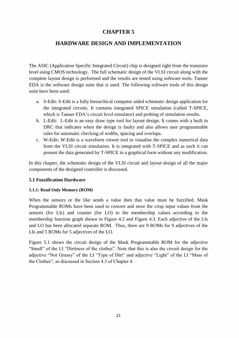
5.1.1: Read Only Memory (ROM)
When the sensors or the like sends a value then that value must be fuzzified. Mask
Programmable ROMs have been used to convert and store the crisp input values from the
sensors (for LIs) and counter (for LO) to the membership values according to the
membership function graph shown in Figure 4.2 and Figure 4.3. Each adjective of the LIs
and LO has been allocated separate ROM. Thus, there are 9 ROMs for 9 adjectives of the
LIs and 5 ROMs for 5 adjectives of the LO.
Figure 5.1 shows the circuit design of the Mask Programmable ROM for the adjective
“Small” of the LI “Dirtiness of the clothes”. Note that this is also the circuit design for the
adjective “Not Greasy” of the LI “Type of Dirt” and adjective “Light” of the LI “Mass of
the Clothes”, as discussed in Section 4.3 of Chapter 4.

22
W0
W1
W2
W3
W4
W5
W6
W7
Bit0Bit1Bit2Bit3Bit4Bit5Bit6Bit7
W8
W9
W10
Figure5.1: Schematic of Mask Programmable ROM for Small “Dirtiness of Clothes”
In figure 5.1, the horizontal lines of the array are known as word line and the vertical lines
are known as the bit lines. The location of NMOS transistor in the memory array
corresponds to a “0” otherwise it is a “1”. During operation, all bit lines are charged to a

23
high voltage (logic 1) due to PMOS transistors which are active low. When all the word
lines are low (logic 0) then the entire bit lines will remain high (logic 1). This is because
NMOS transistors are active high and as such will not have any effect when the gate input is
low. But, when any of the word line is high (logic 1) then it will trigger the NMOS transistor
or transistors connected to it as the gate input will be high. This will cause the bit line to
which the drain of that NMOS is attached, to be pulled low.
For example, if all the word lines (W0-W10) are low then the NMOS transistors will all be
remain inactive. Thus all the bit lines that are high (logic 1) will be the input to the
inverters. This will output bit 1=bit2-bit3=bit4-bit5=bit6=bit7=0.
Whereas, if the first word line (W0) is high and rest (W1-W10) are low then the two NMOS
transistors whose gate input is connected to the first word line will be active. This will cause
bit line 1 and bit line 3 which are connected to the drain of those two NMOS transistors to
be pulled low. All the rest NMOS transistors will remain inactive and as such all other bit
lines will remain high. All the 7 bit lines when passed through the inverter will then output
bit 0=bit2=bit4=bit5=bit6=bit7=0 and bit 1=bit3=1.
Considering the membership function graph of figure 4.2 (a), it can be seen that the graph
for membership function is plotted in accordance to table 5.1. The numbers inside the
parenthesis in table 5.1are the binary equivalent of the listed decimal numbers.
Crisp input value (x axis) Membership grade (Y axis)
0 (00000000) 10 (00001010)
10 (00001010) 8 (00001000)
20 (00010100) 6 (00000110)
30 (00011110) 4 (00000100)
40 (00101000) 2 (00000010)
50 (00110010) 0 (00000000)
60 (00111100) 0 (00000000)
70 (01000110) 0 (00000000)
80 (01010000) 0 (00000000)
90 (01011010) 0 (00000000)
100 (01100100) 0 (00000000)
Table 5.1: Data of the membership function graph for the adjective “small” of the LI
“Dirtiness of the Clothes”
In table 5.1, it can be seen that in order to obtain membership grade value of 10 (00001010)
the crisp input value must be 0 (00000000), in order to obtain membership grade value of 8
(00001000) the crisp input value must be 10 (00001010) and so on. The membership grade
values of table 5.1 are the 8 bit output of the ROM circuit shown in figure 5.1. Each
membership grade value depends upon the configuration of the NMOS transistors and logic
level of word lines (W0 to W10) in ROM circuit of figure 5.1. For example in order to
obtain bit output value 10 (00001010) the bit line values that are the input to the inverters
must be 11110101 and in order to obtain bit line values as 11110101 with the above NMOS
transistor configuration, the word line W0 must be high (logic 1) and the rest of the word
lines (W1 to W10) must be low (logic 0).

24
5.1.2 Word line Select Hardware
This is another hardware that must be designed and interfaced with the masked
programmable ROM in order to obtain fully functional fuzzification hardware. It is
explained in subsection 5.1.1 that the membership values depend upon the configuration of
the NMOS transistors and logic level of word lines. But it also is necessary to design a
circuit that triggers the desired logic level of the word line to be high and rest to remain low
depending upon the sensor values (crisp input values). In other words there must be a circuit
design interfaced to each of the ROMs that selects one of the word lines to be logic 1 and
rest to remain logic 0, depending upon the bit values of the crisp inputs, so that desired
fuzzified values can be obtained.
For example, it can be seen from the table 5.1 that in order to obtain bit output as 00001010
the logic level of the crisp input value must be 00000000. Thus, there needs to be a
hardware interfaced to the ROM circuit of figure 5.1 so that when the crisp input value (or
the sensor value) is 00000000 then word line (W0) turns high and the rest of the word lines
(W1-W10) remains low. Only when this happens, the ROM circuit can output the fuzzified
value of 00001010. The hardware that needs to be interfaced is the Word line Select
hardware. The screen shot of this hardware designed in S-Edit is shown in figure 5.2.
Figure 5.2: Screenshot of Word line selector for Small “Dirtiness of the clothes”
As seen in figure 5.2, there are 8 AND gates. The 8 inputs for each of these AND gates are
the 8 bit values given by sensor (also known as crisp input values) with the right most input
representing the least significant bit of the crisp input value and the left most input
representing the most significant bit of the crisp input value. The 8 bit crisp input values are
either fed directly as input to the AND gates or are fed through the inverters present. The
configuration of the inverter is custom designed according to crisp input values listed on the
first column of table 5.1. The presence of inverter represents “0” and the absence of inverter
represents “1”. These output of these AND gates, from right to left are W0, W1, W2, W3,
W4, W5, W6, W7, W8, W8 and W10.
25
The circuit block on the left are the 8 flip flops whose inputs are S0, S1, S2, S3, S4, S5, S6
and S7.These inputs represent each bit of the 8 bit crisp input values (sensor values)with S0
representing the least significant bit and S7 representing the most significant bit. At each
NGT of the CLK this 8bit values will be transferred as inputs to each of the 8 AND gates.
The word line select hardware (shown in figure 5.2) is interfaced with ROM circuit (shown
in 5.1) in such a way that W0 output port of the former is connected to the W0 input port of
the later, W1 output port of the former is connected to the W1 input port of the later and so
on. The final hardware obtained by interfacing these two hardware is the fuzzification
hardware of the adjective “Small” of the LI “Dirtiness of the clothes”.
Putting it all together:
Here is the example to explain the working of the overall fuzzification hardware:
Let’s assume that the value from the sensor (crisp input value) is 40 (00101000). This means
that the S0-S7 input ports of the D flip flops of Figure 5.2 will be 00101000 (S0 represents
the least significant bit and S7 represents the most significant bit). At the NGT of the clock,
00101000 will be fed to the respective 8 inputs of each of the 8 AND gates (via inverters or
directly).
Moving from right to left in figure 5.2,
When “00101000” is fed to the first AND gate then the inputs to this AND gate will be
“11010111”. Thus, output W0 will be” 0”.
When “00101000” is fed to the second AND gate then the inputs to this AND gate will be
“110111101”. Thus, output W1 will be ”0”.
When “00101000” is fed to the third AND gate then the inputs to this AND gate will be
“11000011”. Thus, output W2 will be”0”.
When “00101000” is fed to the fourth AND gate then the inputs to this AND gate will be
“11001001”. Thus, output W3 will be ”0”.
When “00101000” is fed to the fifth AND gate then the inputs to this AND gate will be
“11111111”. Thus, output W4 will be”1”.
Similarly all the remaining outputs (W5-W10) will be “0”.
Thus, only W4 will be 1 and when, the circuit of figure 5.2 is interfaced with the circuit of
figure 5.1, the word line whose input is W4 will be high. This will cause the NMOS
transistor at the junction of this word line and the bit line 1 (of figure 5.1) to be active. As
the result of this, the bit line 1 will be pulled low and the value of Bit 1 will be “1”. All the
rest of the bits (Bit 0 and Bits 2-7) will be 0. Thus, the output of this fuzzification hardware
will be 00000010 (2 in decimal). This is true as table 5.1 shows that when crisp input value
00101000 then member grade value is 00000010.

26
Fuzzification hardware for all other adjectives of the linguistic inputs is designed with the
same concept. Also, the fuzzification hardware for the 5 adjectives of the linguistic outputs
is designed using the same concept.
5.2 Fuzzy Inference Hardware
Fuzzy Inference hardware is designed to implement the MIN/ MAX operations discussed in
Chapter 4. This hardware takes fuzzified values from each of the fuzzification hardware as
inputs, performs the MIN/MAX operations according to the fuzzy rules and outputs the final
membership output.
5.2.1 Hardware to calculate MIN/MAX
Figure 5.3 shows the MIN/MAX selector circuit that compares two sets (A and B) each
containing 8 bit binary numbers. This hardware then identifies the set having the MIN value
and MAX value. This circuit then outputs high (logic 1) to the MIN set and outputs low
(logic 0) to the MAX set.
Figure5.3 MIN/MAX Selector
If Set A = 00000010 and Set B= 00000110 then input ports "A2”-“A7” will be “0” and
input port A1 will be “1”. Similarly, input ports “B0” & “B3”-“B7” will be “1” and input
ports “B1” & “B2” will be “0”. This circuit then identifies the MIN as well as MAX set and

27
outputs high (logic 1) to output port “Select A” and outputs low (logic 0) to output port
“Select B”. Thus, the output port representing the MIN set will be “high” and the output set
representing the MAX set will be “low”
It can be noted that the least significant bit of set A (which is “A0”) does not have any input
port in figure 5.3. This is because the hardware is designed in such a way that it functions
well regardless of whether this least significant bit for set A is 0 or 1. Thus, it is grounded
and not included/connected anywhere in the MIN/MAX selector hardware.
The MIN/MAX selector hardware then needs to be interfaced with another hardware so that
the 8 bit values of the MIN (or MAX) set comes out as the resulting output of the complete
MIN/MAX calculation hardware. This second hardware that needs to be interfaced is named
as “Bit Selector” and is shown in figure 5.4.
Select A
Select B
A7
B7
A6
A5
B5
A4
B4
A3
B3
A2
A1
B1
A0
B2
B0
B6
Bit7
Bit6
Bit5
Bit4
Bit3
Bit2
Bit1
Bit0
Figure 5.4: Bit selector hardware
“Bit selector” hardware of figure 5.4 outputs 8 bits of Set A (if Select A is “1”) or 8 bits of
Set B (if Select B is “1”).
When the hardware of figure 5.3 is interfaced with the hardware of figure 5.4 in such a way
that output ports “Select A” and “Select B” of Figure 5.3 are connected respectively to the
input ports “Select A” and “Select B” of Figure 5.4, then the resulting output (outputs from
output ports Bit 0- Bit7) that is generated will be the 8 bits of the MIN set. This is because
high (logic 1) output port of figure 5.3 represents the MIN set and low (logic 0) output
represents the MAX set, as discussed before. Thus, the complete hardware obtained by
interfacing the hardware of Figure 5.3 with the hardware of Figure 5.4 will be the complete
MIN calculation hardware.
However, when the “Select A” output port and “Select B” output port of figure 5.3 are
interchanged (or swapped) , the output port which results high (logic 1) will represent the
MAX set and the output port which results low (logic 0) will represent the MIN set. This

28
hardware with swapped output ports when interfaced with the “Bit selector” hardware of
figure 5.4 will output the 8 bits of the MAX set as the resulting outputs. Thus, it will now
become the complete MAX calculation hardware.
Figure 5.5 shows the layout design of the complete MIN/MAX calculation hardware,
designed using L-Edit.
Figure 5.5: Layout design of a complete MIN/MAX calculation hardware
In order to perform the fuzzy inference process for this controller, there are 4 sets of 8 bit
fuzzified outputs for each of the fuzzy rules that need to be compared to determine the 8 bit
set containing the least value (MIN value). This is because each of the fuzzy rules has 3
premises and 1 conclusion in the form of:

29
Rule A: IF (Premise_1) AND (Premise_2) AND (Premise_3) THEN (Conclusion _A)
The hardware that can compare 4 different sets (3 for premises and 1 for conclusion) and
output the set representing the least (MIN) value among 4 sets is obtained by combining 3
complete MIN calculation hardware in a way as shown in Figure 5.6.

30
Figure 5.6: Block diagram showing working of MIN calculation hardware to compare 4 sets
of 8 bit binary numbers
Complete MIN Calculation Hardware 1
Complete MIN Calculation Hardware 2
Complete MIN Calculation Hardware 3
First Set of Fuzzified Output
(8 bit for Premise_1)
Second Set of Fuzzified Output
(8 bit for Premise_ 2)
Third Set of Fuzzified Output
(8 bit for Premise_ 3)
Fourth Set of Fuzzified Output
(8 bit for Conclusion)
MIN Set (First Set VS
Second Set)
Final MIN set
MIN Set (First Set VS
Second Set VS Third
Set)
31
In Figure 5.6 it can be seen that three “complete MIN calculation hardware” can be
combined to obtain MIN hardware that can compare 4 sets and output the most MIN set as
the result. Thus, there needs to be a total of 27 MIN calculation hardware each of which can
compare 4 sets of 8 bit fuzzified output. This is because there are 27 different fuzzy rules
and each rule contains 4 sets (3 for premises and 1 for conclusion).
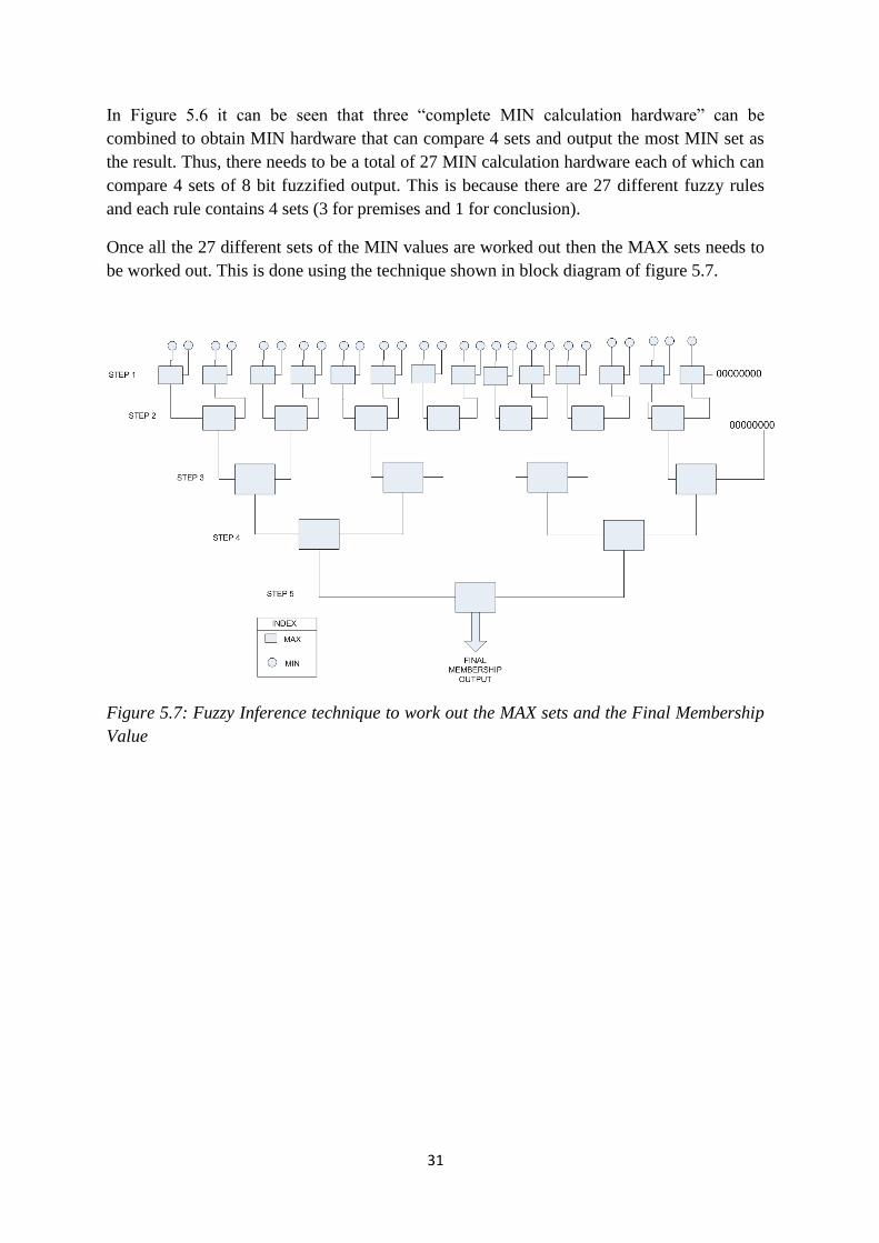
Once all the 27 different sets of the MIN values are worked out then the MAX sets needs to
be worked out. This is done using the technique shown in block diagram of figure 5.7.
Figure 5.7: Fuzzy Inference technique to work out the MAX sets and the Final Membership
Value
32
In Figure 5.7 the circles denote the MIN calculation hardware that can compare 4 sets of 8
bit number and output the most MIN set as the result as discussed before. It can be seen that
there are 27 of them. The 5 steps are shown in Figure 5.7 is the hardware design method that
compares all the 27 sets and outputs the one which holds the highest (MAX) value among
them. Each of the steps shown is figure 5.7 is explained below:
STEP 1: 26 output sets from the MIN calculation hardware are divided into 13 pairs
and each pair is fed onto the13 individual MAX calculation hardware. The 27th
output set from the MIN calculation hardware is paired with the set representing
00000000 and fed onto the separate MAX calculation hardware. Therefore, there is a
total of 14 MAX calculation hardware in this step. Each of the MAX calculation
hardware compares 2 different sets and outputs the one representing the highest
value as a result.
STEP 2: 14 different output sets of Step 1 are divided into 7 pairs and each pair is
fed into 7 individual MAX calculation hardware. Each of the MAX calculation
hardware compares 2 different sets and outputs the one representing the highest
value as a result.
STEP 3: 7 different output sets of step 2 are divided into 3 pairs and each pair is fed
into 3 individual MAX calculation hardware. The 7th
output set is paired with the set
representing 00000000 and fed onto the separate MAX calculation hardware.
Therefore, there is a total of 4 MAX calculation hardware in this step. Each of the
MAX calculation hardware compares 2 different sets and outputs the one
representing the highest value as a result.
STEP 4: 4 different output sets of step 3 are divided into 2 pairs and each pair is fed
into 2 individual MAX calculation hardware. Each of the MAX calculation hardware
compares 2 different sets and output the one representing the highest value as a
result.
STEP 5: 2 different output sets of step 4 is fed into the final MAX calculation
hardware and this final 8 bit set obtained is the set representing the highest value
among the 27 different sets and is called the “final membership output”.
The final membership output is the final output of the “fuzzy inference hardware” (also
known as “fuzzy inference engine”). The layout design of the complete fuzzy inference
hardware which is designed using L-Edit is shown is Figure 5.8.

33
Figure 5.8: Layout design of the fuzzy inference hardware
34
5.3 Defuzzification Hardware
As discussed in Chapter 4, Defuzzifier is used to obtain the final crisp output (Cout) which
is the Wash time and is given by,
Where, i0- i12 are the counter output that counts from 0 to 12 and m0-m12 are the final
membership value of the fuzzy inference hardware corresponding to the count 0-12. (In
other words, m0 corresponds to the final membership value when counter counts 0, m1
correspond to the final membership value when counter counts 1 and so on).
Defuzzification hardware is the one that does the calculation shown in the above equation to
work out the final crisp output value (Wash Time)
Just by looking at the equation it can be seen that the defuzzification hardware requires a
MOD 13 counter (to count from 0 to 12), a multiplier (to multiply the membership values
with the counter values), a full adder (for addition) and a divider for division. Design of
each of the hardware will be discussed in this section. Also, the interfacing of all hardware
to design the dividend (numerator) and the divisor (denominator) part of the equation will be
discussed.
5.3.1 MOD-13 counter
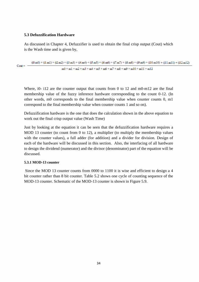
Since the MOD 13 counter counts from 0000 to 1100 it is wise and efficient to design a 4
bit counter rather than 8 bit counter. Table 5.2 shows one cycle of counting sequence of the
MOD-13 counter. Schematic of the MOD-13 counter is shown in Figure 5.9.
35
Table 5.2: Cycle of counting sequence of the MOD- 13 counter
J
K
J
K K
J J
K
Q3 Q2 Q1 Q0
CLRCLR CLR CLR
33 MHz
Q3 Q2 Q1 Q0
Figure 5.9: Synchronous MOD-13 counter
COUNT Q3 Q2 Q1 Q0
0 0 0 0 0
1 0 0 0 1
2 0 0 1 0
3 0 0 1 1
4 0 1 0 0
5 0 1 0 1
6 0 1 1 0
7 0 1 1 1
8 1 0 0 0
9 1 0 0 1
10 1 0 1 0
11 1 0 1 1
12 1 1 0 0
0 0 0 0 0

36
It can be seen in Figure 5.9 that the CLK (Clock) inputs of all the flip-flops are connected
together so that the input clock signal is applied to each flip-flops simultaneously. Only, the
right most flip-flop, the LSB, has its J and K inputs permanently at the “high” level. The J,
K inputs of the other flip flops are driven by some combination of flip-flop outputs.
The counting sequence on Table 5.2 shows that the right-most flip-flop must change states
at each negative (High to Low) transition made by the clock pulse. For this reason, its J and
K inputs are permanently high so that it will toggle on each NGT of the clock input.
The counting sequence shows that second from right flip-flop must change states on NGT
that occurs while Q0=1. For example, when the count is 0001, the next NGT must toggle Q1
to the 1 state; when the count is 0011, the next NGT must toggle Q1 to the 0 state; and so
on. This operation is accomplished by connecting output Q0 to the J and K inputs of the
second from right flip flop so that J=K=1 only when Q0=1.
The counting sequence shows that third from right flip-flop must change states on each
NGT that occurs while Q0=Q1=1. For example, when the count is 0011, the next NGT must
toggle Q3 to the 1 state; when the count is 0111, the next NGT must toggle Q2 to the 0
state; and so on. By connecting the output of the AND gate (whose inputs are Q0 and Q1) to
this flip-flop‟s J and K inputs, this flip-flop will toggle only when Q0=Q1=1.
In a like manner, we can see that the left-most flip flop must toggle on each NGT that
occurs while Q0=Q1=Q2=1. When the count is 0111, the next NGT must toggle Q3 to the 1
state. By connecting the AND gate (whose inputs are Q0, Q1 and Q2) to this flip-flip‟s J and
K inputs, this flip-flop will only toggle when Q0=Q1=Q2=1. Also, it is to be noted that
when the count is 1101 then the AND gate (whose output is connected to CLR) will have its
output as 1 and the clear function is activated. This will reset the counter back to its initial
state which is 0000.
5.3.2 Full Adder
The full adder has 3 inputs (A, B and Cin) and two outputs (Sum and Cout) as shown in
Figure 5.10.It adds the three binary input numbers to produce sum and carry-out terms. The
truth table for this design is shown in Table 5.3.
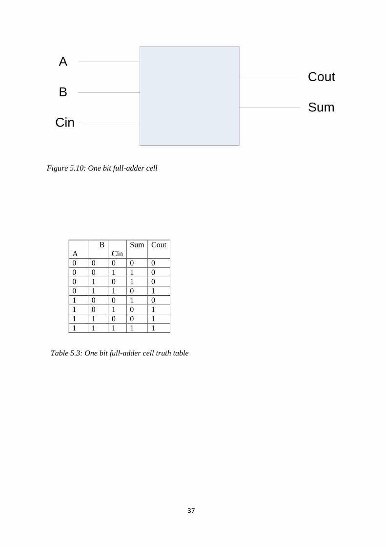
37
A
B
Cin
Cout
Sum
Figure 5.10: One bit full-adder cell
Table 5.3: One bit full-adder cell truth table
A
B
Cin
Sum Cout
0 0 0 0 0
0 0 1 1 0
0 1 0 1 0
0 1 1 0 1
1 0 0 1 0
1 0 1 0 1
1 1 0 0 1
1 1 1 1 1
38
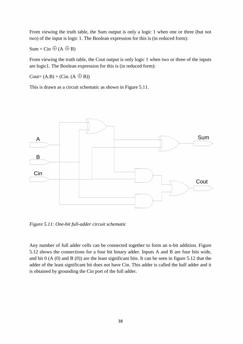
From viewing the truth table, the Sum output is only a logic 1 when one or three (but not
two) of the input is logic 1. The Boolean expression for this is (in reduced form):
Sum = Cin (A B)
From viewing the truth table, the Cout output is only logic 1 when two or three of the inputs
are logic1. The Boolean expression for this is (in reduced form):
Cout= (A.B) + (Cin. (A B))
This is drawn as a circuit schematic as shown in Figure 5.11.
Sum
Cout
A
B
Cin
Figure 5.11: One-bit full-adder circuit schematic
Any number of full adder cells can be connected together to form an n-bit addition. Figure
5.12 shows the connections for a four bit binary adder. Inputs A and B are four bits wide,
and bit 0 (A (0) and B (0)) are the least significant bits. It can be seen in figure 5.12 that the
adder of the least significant bit does not have Cin. This adder is called the half adder and it
is obtained by grounding the Cin port of the full adder.
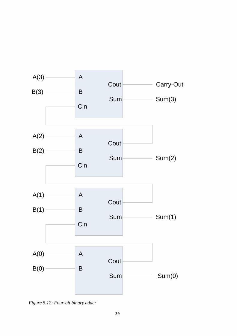
39
A
B
Cin
Cout
Sum
A
B
Cin
Cout
Sum
A
B
Cin
Cout
Sum
A
B
Cout
Sum
A(3)
B(3)
Carry-Out
Sum(3)
Sum(2)
A(2)
B(2)
A(1)
B(1)
A(0)
B(0)
Sum(1)
Sum(0)
Figure 5.12: Four-bit binary adder
40
5.3.3 Multiplier
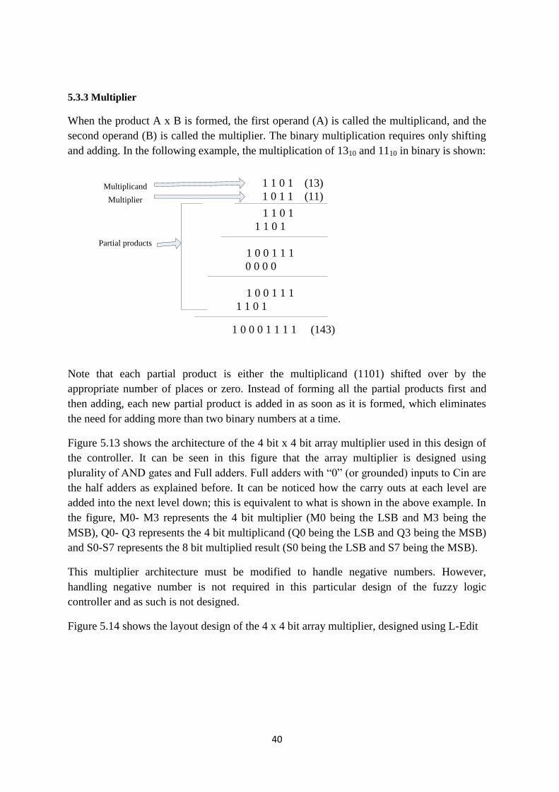
When the product A x B is formed, the first operand (A) is called the multiplicand, and the
second operand (B) is called the multiplier. The binary multiplication requires only shifting
and adding. In the following example, the multiplication of 1310 and 1110 in binary is shown:
1 1 0 1 (13)
1 0 1 1 (11)
1 1 0 1
1 1 0 1
1 0 0 1 1 1
0 0 0 0
1 0 0 1 1 1
1 1 0 1
1 0 0 0 1 1 1 1 (143)
Multiplicand
Multiplier
Partial products
Note that each partial product is either the multiplicand (1101) shifted over by the
appropriate number of places or zero. Instead of forming all the partial products first and
then adding, each new partial product is added in as soon as it is formed, which eliminates
the need for adding more than two binary numbers at a time.
Figure 5.13 shows the architecture of the 4 bit x 4 bit array multiplier used in this design of
the controller. It can be seen in this figure that the array multiplier is designed using
plurality of AND gates and Full adders. Full adders with “0” (or grounded) inputs to Cin are
the half adders as explained before. It can be noticed how the carry outs at each level are
added into the next level down; this is equivalent to what is shown in the above example. In
the figure, M0- M3 represents the 4 bit multiplier (M0 being the LSB and M3 being the
MSB), Q0- Q3 represents the 4 bit multiplicand (Q0 being the LSB and Q3 being the MSB)
and S0-S7 represents the 8 bit multiplied result (S0 being the LSB and S7 being the MSB).
This multiplier architecture must be modified to handle negative numbers. However,
handling negative number is not required in this particular design of the fuzzy logic
controller and as such is not designed.
Figure 5.14 shows the layout design of the 4 x 4 bit array multiplier, designed using L-Edit

41
AB
CinCout
Sum
AB
CinCout
Sum
AB
CinCout
Sum
AB
CinCout
Sum
AB
CinCout
Sum
AB
CinCout
Sum
AB
CinCout
Sum
AB
CinCout
Sum
AB
CinCout
Sum
AB
CinCout
Sum
AB
CinCout
Sum
AB
CinCout
Sum
Q0Q1Q2Q3
Q0Q1Q2Q3
Q0Q1Q2Q3
Q0Q1Q2Q3
“0”
“0”
“0”
S0S1S2S3S4S5S6S7
Q3 Q2 Q1 Q0
M0
M1
M2
M3
Figure 5.13: A 4x4 bit array multiplier
42
Figure 5.14: Layout design of the 4x4 bit array multiplier
5.3.4 Dividend Hardware
The following block diagram explains the functioning of the dividend hardware:
Register 1Register 2
Full Adder
Register 3
Multiplier
MOD 13 counter (4
bit)
Final member value (4
bit)
Figure 5.15: Functioning of the hardware to calculate the dividend

43
The maximum value that the final member value can have is 12 (1100). As such only the 4
least significant bits of the 8 bit final member value obtained from the fuzzy inference
hardware is taken into consideration. The other 4 most significant bits of this hardware will
be zero so is ignored. This 4 bit final member value is fed inside the multiplier and is
multiplied with the 4 bit output of the MOD 13 counter. At each NGT of the clock the
counter will change its output and each of these outputs will be multiplied with the
corresponding final member value at that particular count of the counter. Registers 1,
Register 2 and Register 3 are 11 bits each and each of them are designed by simply
connecting 11 D flip-flops in series. Note that the clocks of Registers 1 and 2 are connected
together to the clock of the counter and the clock is fed into the inverter whose output is
then connected to the clock input of Register 3.The following steps explain the operation of
the dividend circuit:
STEP 1: At 1st NGT of the clock, the output from the multiplier will be fed to Register 1. At
this point all 11 bits of Register 2 will be zero. The value of Registers 1 and 3 will be added
by the full adder. The output of the full adder is fed into Register 3 only at PGT of the clock.
STEP 2: At 2nd
NGT of the clock, the new output from the multiplier will be fed to Register
1. At this point all 11 bits of Register 3 obtained in STEP 1 will be transferred to Register 2.
This 11 bit set from the Register 2 will be added with new 11 bit set of Register 1. The
output of the full adder is fed into Register 3 only at PGT of the clock.
STEP 3: At 3rd
NGT of the clock, the new output from the multiplier will be fed to Register
1. At this point all 11 bits of Register 3 obtained in STEP 2 will be transferred to Register 2.
This 11 bit set from the Register 2 will be added with new 11 bit set of Register 1. The
output of the full adder is fed into Register 3 only at PGT of the clock.
…………………………………………………………………………………………………
…………………………………………………………………………………………………
…………………………………………………………………………………………………
…………………………………………………………………………………………………
…………………………………………………………………………………………………
…………………………………………………………………………………………………
…………………………………………………………………………………………………
…………………………………………………………………………………………………
STEP 12: At 12th
NGT of the clock, the new output from the multiplier will be fed to
Register 1. At this point all 11 bits of Register 3 obtained in STEP 11 will be transferred to
Register 2. This 11 bit set from the Register 2 will be added with new 11 bit set of Register
1. The output of the full adder is fed into Register 3 only at PGT of the clock. This will be
the final value for the dividend hardware.
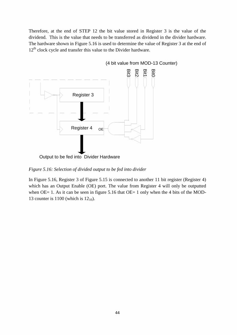
44
Therefore, at the end of STEP 12 the bit value stored in Register 3 is the value of the
dividend. This is the value that needs to be transferred as dividend in the divider hardware.
The hardware shown in Figure 5.16 is used to determine the value of Register 3 at the end of
12th
clock cycle and transfer this value to the Divider hardware.
OE
Register 3
Register 4
Bit0
Bit1
Bit2
Bit3
(4 bit value from MOD-13 Counter)
Output to be fed into Divider Hardware
Figure 5.16: Selection of divided output to be fed into divider
In Figure 5.16, Register 3 of Figure 5.15 is connected to another 11 bit register (Register 4)
which has an Output Enable (OE) port. The value from Register 4 will only be outputted
when OE= 1. As it can be seen in figure 5.16 that OE= 1 only when the 4 bits of the MOD-
13 counter is 1100 (which is 1210).
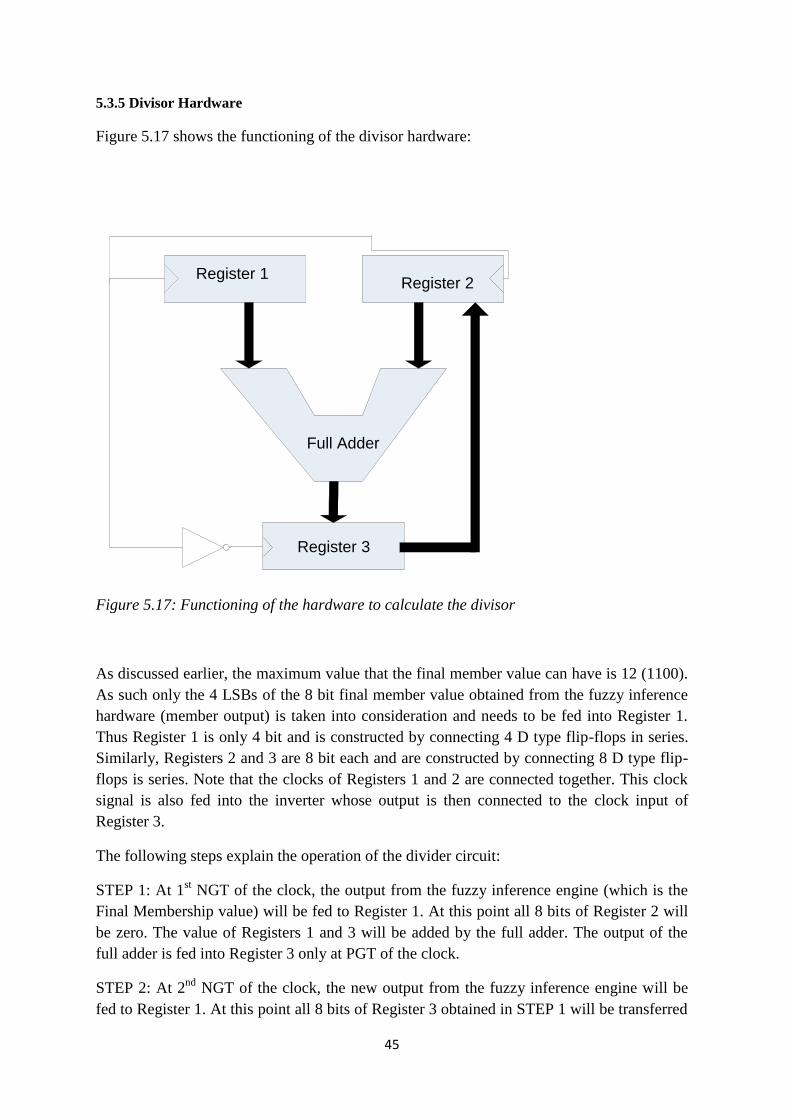
45
5.3.5 Divisor Hardware
Figure 5.17 shows the functioning of the divisor hardware:
Register 1Register 2
Full Adder
Register 3
Figure 5.17: Functioning of the hardware to calculate the divisor
As discussed earlier, the maximum value that the final member value can have is 12 (1100).
As such only the 4 LSBs of the 8 bit final member value obtained from the fuzzy inference
hardware (member output) is taken into consideration and needs to be fed into Register 1.
Thus Register 1 is only 4 bit and is constructed by connecting 4 D type flip-flops in series.
Similarly, Registers 2 and 3 are 8 bit each and are constructed by connecting 8 D type flip-
flops is series. Note that the clocks of Registers 1 and 2 are connected together. This clock
signal is also fed into the inverter whose output is then connected to the clock input of
Register 3.
The following steps explain the operation of the divider circuit:
STEP 1: At 1st NGT of the clock, the output from the fuzzy inference engine (which is the
Final Membership value) will be fed to Register 1. At this point all 8 bits of Register 2 will
be zero. The value of Registers 1 and 3 will be added by the full adder. The output of the
full adder is fed into Register 3 only at PGT of the clock.
STEP 2: At 2nd
NGT of the clock, the new output from the fuzzy inference engine will be
fed to Register 1. At this point all 8 bits of Register 3 obtained in STEP 1 will be transferred

46
to Register 2 and will be added with new 8 bit set of Register 1. The output of the full adder
is fed into Register 3 only at PGT of the clock.
STEP 3: At 3rd
NGT of the clock, the new output from the fuzzy inference engine will be
fed to Register 1. At this point all 8 bits of Register 3 obtained in STEP 2 will be
transferred to Register 2 and will be added with new 8 bit set of Register 1. The output of
the full adder is fed into Register 3 only at PGT of the clock.
…………………………………………………………………………………………………
…………………………………………………………………………………………………
…………………………………………………………………………………………………
…………………………………………………………………………………………………
…………………………………………………………………………………………………
…………………………………………………………………………………………………
…………………………………………………………………………………………………
…………………………………………………………………………………………………
STEP 12: At 12th
NGT of the clock, the new output from the fuzzy inference engine will be
fed to Register 1. At this point all 8 bits of Register 3 obtained in STEP 11 will be
transferred to Register 2 and will be added with new 8 bit set of Register 1. The output of
the full adder is fed into Register 3 only at PGT of the clock. This will be the final value for
the divisor hardware.
Therefore, at the end of STEP 12 the bit value stored in Register 3 is the value of the
dividend. Hardware almost identical to the one in figure 5.16 (only difference is that
Register 4 is 8 bit instead of 12 bit) needs to be connected to Register 3 of figure 5.17 in
order to determine the value of Register 3 at the end of 12th
clock cycle and transfer this
value to the Divider hardware.
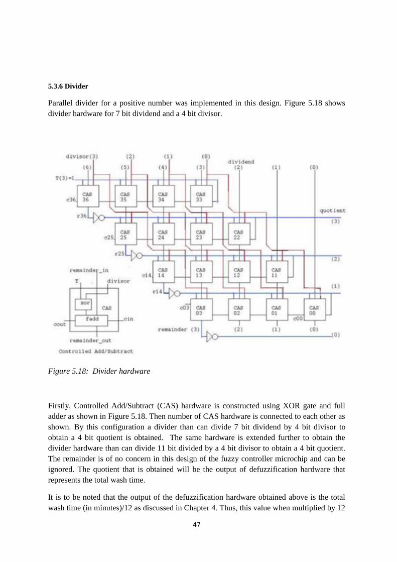
47
5.3.6 Divider
Parallel divider for a positive number was implemented in this design. Figure 5.18 shows
divider hardware for 7 bit dividend and a 4 bit divisor.
Figure 5.18: Divider hardware
Firstly, Controlled Add/Subtract (CAS) hardware is constructed using XOR gate and full
adder as shown in Figure 5.18. Then number of CAS hardware is connected to each other as
shown. By this configuration a divider than can divide 7 bit dividend by 4 bit divisor to
obtain a 4 bit quotient is obtained. The same hardware is extended further to obtain the
divider hardware than can divide 11 bit divided by a 4 bit divisor to obtain a 4 bit quotient.
The remainder is of no concern in this design of the fuzzy controller microchip and can be
ignored. The quotient that is obtained will be the output of defuzzification hardware that
represents the total wash time.
It is to be noted that the output of the defuzzification hardware obtained above is the total
wash time (in minutes)/12 as discussed in Chapter 4. Thus, this value when multiplied by 12
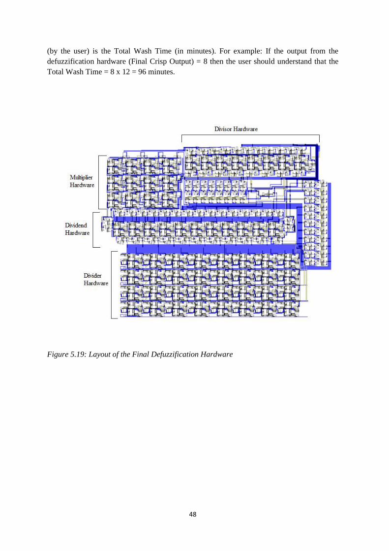
48
(by the user) is the Total Wash Time (in minutes). For example: If the output from the
defuzzification hardware (Final Crisp Output) = 8 then the user should understand that the
Total Wash Time = 8 x 12 = 96 minutes.
Figure 5.19: Layout of the Final Defuzzification Hardware

49
5.4: Overall Hardware Implementation
The overall hardware implementation of the fuzzy controller is shown in figure 5.20. It can
be seen that the inputs from the sensor (or the like) is fed into the 9 ROMs for the LIs at the
same time when the counter value of the MOD-13 counter is fed into the 5 ROMs for LO.
Then the fuzzified values from the ROMs will be fed into the fuzzy inference engine. The
output of the fuzzy inference engine is known as membership output which will be fed into
the defuzzification hardware which consists of Multiplier, Divisor hardware, Dividend
hardware and Divider hardware. The output from the Dividend hardware and Divider
hardware is fed into the divider and the output of the divider will be the final “Wash Time”
value. This value is the overall output of the fuzzy logic controller hardware. The user then
multiplies this value by 12 to obtain the total wash time in minutes.
Fuzzy Inference Engine
Divider
MOD-13
Counter
9 ROMs for Linguistic
Inputs
5 R
OM
s fo
r Lin
gu
istic
Ou
tpu
t
Divisor Hardware
Dividend Hardware
Wash Time
33 MHz
Multiplier
CLKSensor Inputs
Figure 5:20: Complete hardware implementation of the Fuzzy Logic Controller
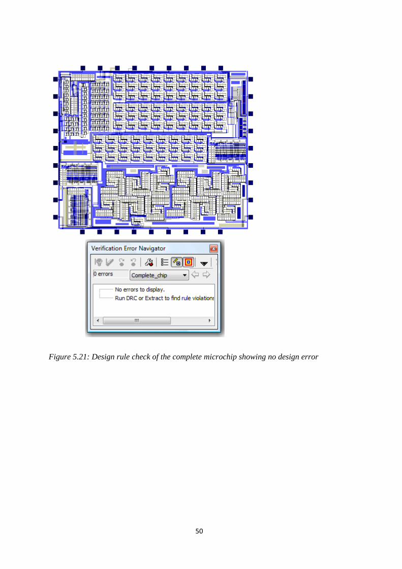
50
Figure 5.21: Design rule check of the complete microchip showing no design error

51
INDEX
WT= Wash Time
DS= Dirtiness of the Clothes
MS= Mass of the Clothes
GS= Greasiness of the Clothes
Figure 5.22: Labelled layout of the complete Microchip

52
CHAPTER 6
SIMULATION STUDY
SPICE has become the industry standard for computer –aided circuit analysis for
microelectronic circuits, and is used by the majority of IC designers (Roberts, 1997). T-
SPICE is used as a simulation tool in the circuit simulation in this design as it is the
simulation tool for Tanner EDA.
Major drawback of T-Spice is that this tool is not suitable for the simulation of large
circuits. Thus, the simulation of the full microcontroller circuit that contains over 30,000
transistors cannot be achieved. But, the tool works perfectly for the simulation and graphical
analysis of smaller circuits. In this chapter the simulation results of the 4 major hardware
components that were designed will be discussed. The operations of all other hardware
components are self explanatory.
6.1 Simulation study of MAX Hardware
Here,
A= 01000000
B= 0 1111110
After, the simulation of the MAX circuit the following 8 graphs are obtained:
Figure 6.1 (a) Simulation Result of MAX circuit output showing Bit 0 ≈ 0V (Logic 0)
0 10 20 30 40 50 60 70 80 90 100
Time (ns)
-100
-50
0
50
100
150
Vo
ltag
e (
nV
)
Complete Maximim Circuit (Bit 0)
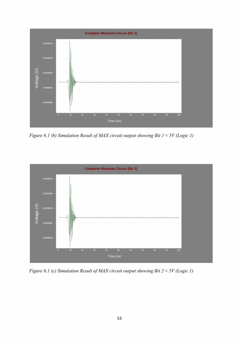
53
Figure 6.1 (b) Simulation Result of MAX circuit output showing Bit 1 ≈ 5V (Logic 1)
Figure 6.1 (c) Simulation Result of MAX circuit output showing Bit 2 ≈ 5V (Logic 1)
0 10 20 30 40 50 60 70 80 90 100
Time (ns)
4.99999990
4.99999995
5.00000000
5.00000005
5.00000010
Vo
ltag
e (
V)
Complete Maximim Circuit (Bit 1)
0 10 20 30 40 50 60 70 80 90 100
Time (ns)
4.99999990
4.99999995
5.00000000
5.00000005
5.00000010
Vo
ltag
e (
V)
Complete Maximim Circuit (Bit 2)
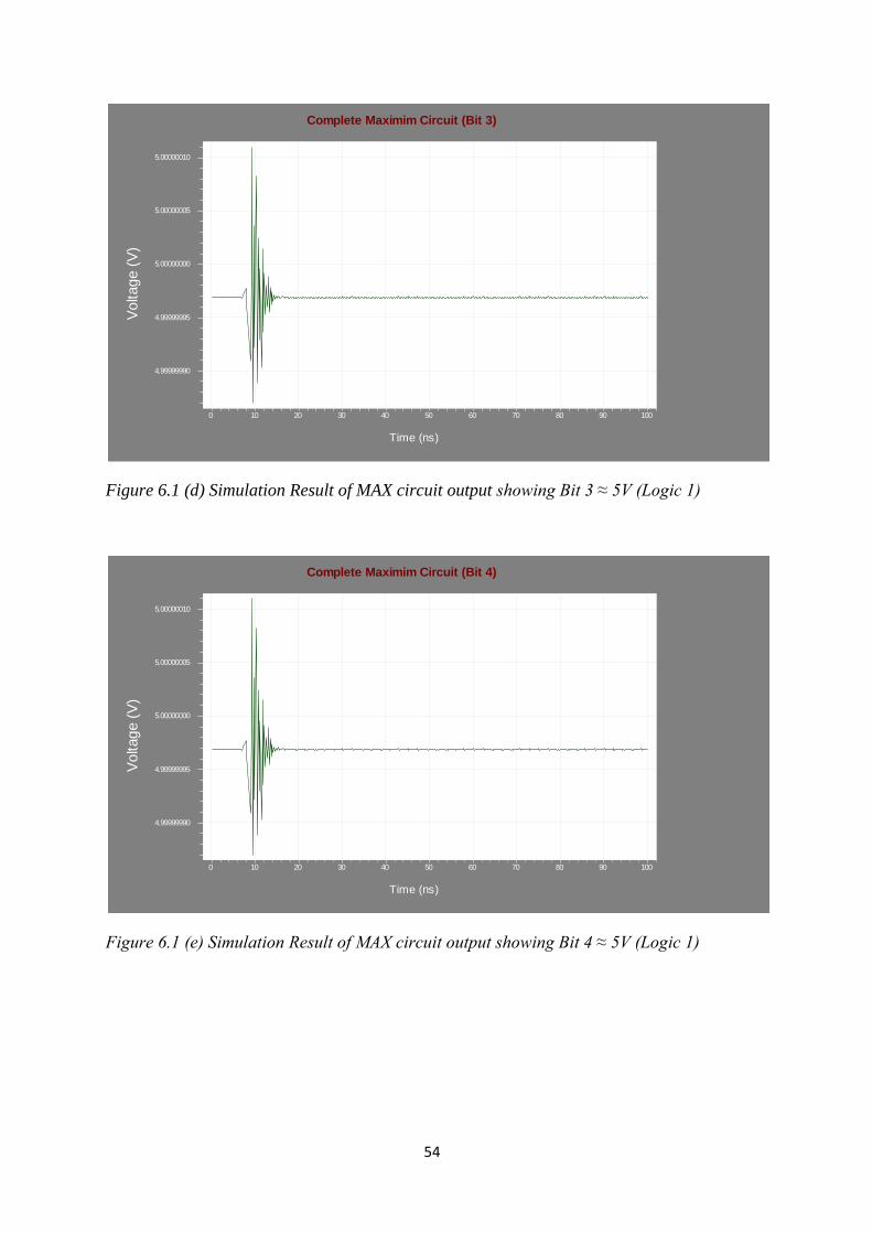
54
Figure 6.1 (d) Simulation Result of MAX circuit output showing Bit 3 ≈ 5V (Logic 1)
Figure 6.1 (e) Simulation Result of MAX circuit output showing Bit 4 ≈ 5V (Logic 1)
0 10 20 30 40 50 60 70 80 90 100
Time (ns)
4.99999990
4.99999995
5.00000000
5.00000005
5.00000010
Vo
ltag
e (
V)
Complete Maximim Circuit (Bit 3)
0 10 20 30 40 50 60 70 80 90 100
Time (ns)
4.99999990
4.99999995
5.00000000
5.00000005
5.00000010
Vo
ltag
e (
V)
Complete Maximim Circuit (Bit 4)

55
Figure 6.1 (f) Simulation Result of MAX circuit output showing Bit 5 ≈ 5V (Logic 1)
Figure 6.1 (g) Simulation Result of MAX circuit output showing Bit 6 ≈ 5V (Logic 1)
0 10 20 30 40 50 60 70 80 90 100
Time (ns)
4.99999990
4.99999995
5.00000000
5.00000005
5.00000010
Vo
ltag
e (
V)
Complete Maximim Circuit (Bit 5)
0 10 20 30 40 50 60 70 80 90 100
Time (ns)
4.99999990
4.99999995
5.00000000
5.00000005
5.00000010
Vo
ltag
e (
V)
Complete Maximim Circuit (Bit 6)
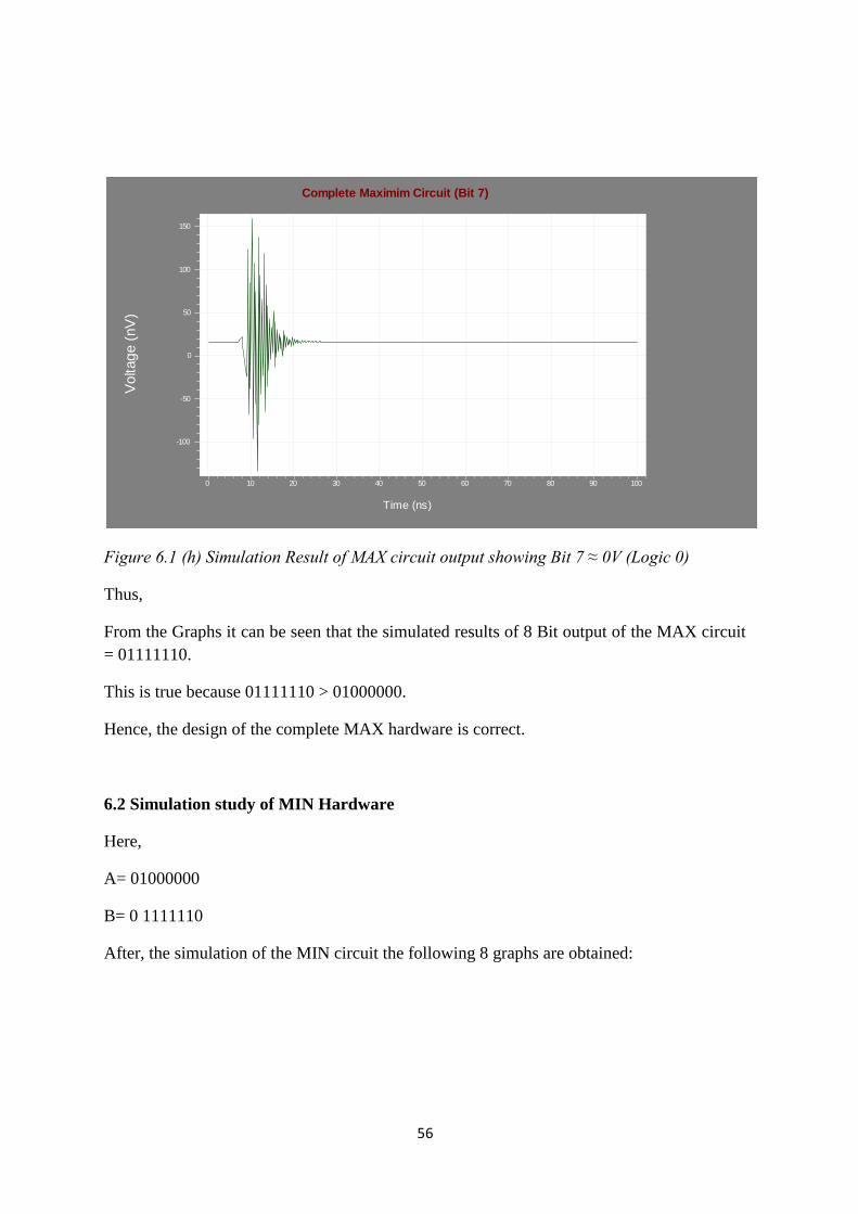
56
Figure 6.1 (h) Simulation Result of MAX circuit output showing Bit 7 ≈ 0V (Logic 0)
Thus,
From the Graphs it can be seen that the simulated results of 8 Bit output of the MAX circuit
= 01111110.
This is true because 01111110 > 01000000.
Hence, the design of the complete MAX hardware is correct.
6.2 Simulation study of MIN Hardware
Here,
A= 01000000
B= 0 1111110
After, the simulation of the MIN circuit the following 8 graphs are obtained:
0 10 20 30 40 50 60 70 80 90 100
Time (ns)
-100
-50
0
50
100
150
Vo
ltag
e (
nV
)
Complete Maximim Circuit (Bit 7)

57
Figure 6.2 (a) Simulation Result of MIN circuit output showing Bit 0 ≈ 0V (Logic 0)
Figure 6.2 (b) Simulation Result of MIN circuit output showing Bit 1 ≈ 0V (Logic 0)
0 10 20 30 40 50 60 70 80 90 100
Time (ns)
-100
-50
0
50
100
150
Vo
ltag
e (
nV
)Complete Minimum Circuit (Bit 0)
0 10 20 30 40 50 60 70 80 90 100
Time (ns)
-100
-50
0
50
100
150
Vo
ltag
e (
nV
)
Complete Minimum Circuit (Bit 1)

58
Figure 6.2 (c) Simulation Result of MIN circuit output showing Bit 2 ≈ 0V (Logic 0)
Figure 6.2 (d) Simulation Result of MIN circuit output showing Bit 3 ≈ 0V (Logic 0)
0 10 20 30 40 50 60 70 80 90 100
Time (ns)
-100
-50
0
50
100
150
Vo
ltag
e (
nV
)Complete Minimum Circuit (Bit 2)
0 10 20 30 40 50 60 70 80 90 100
Time (ns)
-100
-50
0
50
100
150
Vo
ltag
e (
nV
)
Complete Minimum Circuit (Bit 3)

59
Figure 6.2 (e) Simulation Result of MIN circuit output showing Bit 4 ≈ 0V (Logic 0)
Figure 6.2 (f) Simulation Result of MIN circuit output showing Bit 5 ≈ 0V (Logic 0)
0 10 20 30 40 50 60 70 80 90 100
Time (ns)
-100
-50
0
50
100
150
Vo
ltag
e (
nV
)Complete Minimum Circuit (Bit 4)
0 10 20 30 40 50 60 70 80 90 100
Time (ns)
-100
-50
0
50
100
150
Vo
ltag
e (
nV
)
Complete Minimum Circuit (Bit 5)

60
Figure 6.2 (g) Simulation Result of MIN circuit output showing Bit 6 ≈ 5V (Logic 5)
Figure 6.2 (h) Simulation Result of MIN circuit output showing Bit 7 ≈ 0V (Logic 0)
0 10 20 30 40 50 60 70 80 90 100
Time (ns)
4.99999990
4.99999995
5.00000000
5.00000005
Vo
ltag
e (
V)
Complete Minimum Circuit (Bit 6)
0 10 20 30 40 50 60 70 80 90 100
Time (ns)
-100
-50
0
50
100
150
Vo
ltag
e (
nV
)
Complete Minimum Circuit (Bit 7)
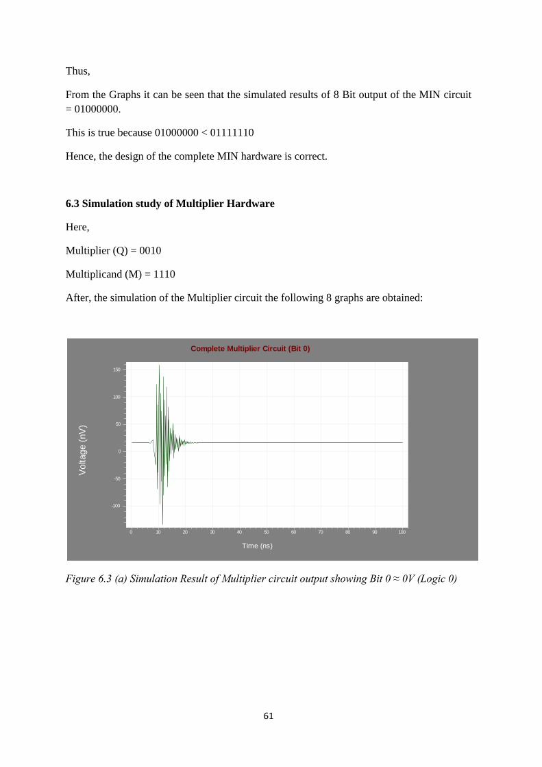
61
Thus,
From the Graphs it can be seen that the simulated results of 8 Bit output of the MIN circuit
= 01000000.
This is true because 01000000 < 01111110
Hence, the design of the complete MIN hardware is correct.
6.3 Simulation study of Multiplier Hardware
Here,
Multiplier (Q) = 0010
Multiplicand (M) = 1110
After, the simulation of the Multiplier circuit the following 8 graphs are obtained:
Figure 6.3 (a) Simulation Result of Multiplier circuit output showing Bit 0 ≈ 0V (Logic 0)
0 10 20 30 40 50 60 70 80 90 100
Time (ns)
-100
-50
0
50
100
150
Vo
ltag
e (
nV
)
Complete Multiplier Circuit (Bit 0)

62
Figure 6.3 (b) Simulation Result of Multiplier circuit output showing Bit 1 ≈ 0V (Logic 0)
Figure 6.3 (c) Simulation Result of Multiplier circuit output showing Bit 2 ≈ 5V (Logic 5)
0 10 20 30 40 50 60 70 80 90 100
Time (ns)
-100
-50
0
50
100
150
Vo
ltag
e (
nV
)
Complete Multiplier Circuit (Bit 1)
0 10 20 30 40 50 60 70 80 90 100
Time (ns)
4.99999990
4.99999995
5.00000000
5.00000005
Vo
ltag
e (
V)
Complete Multiplier Circuit (Bit 2)
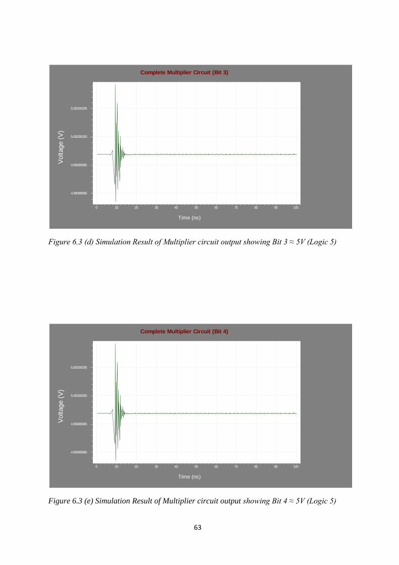
63
Figure 6.3 (d) Simulation Result of Multiplier circuit output showing Bit 3 ≈ 5V (Logic 5)
Figure 6.3 (e) Simulation Result of Multiplier circuit output showing Bit 4 ≈ 5V (Logic 5)
0 10 20 30 40 50 60 70 80 90 100
Time (ns)
4.99999990
4.99999995
5.00000000
5.00000005
Vo
ltag
e (
V)
Complete Multiplier Circuit (Bit 3)
0 10 20 30 40 50 60 70 80 90 100
Time (ns)
4.99999990
4.99999995
5.00000000
5.00000005
Vo
ltag
e (
V)
Complete Multiplier Circuit (Bit 4)

64
Figure 6.3 (f) Simulation Result of Multiplier circuit output showing Bit 5 ≈ 0V (Logic 0)
Figure 6.3 (g) Simulation Result of Multiplier circuit output showing Bit62 ≈ 0V (Logic 0)
0 10 20 30 40 50 60 70 80 90 100
Time (ns)
-100
-50
0
50
100
150
Vo
ltag
e (
nV
)
Complete Multiplier Circuit (Bit 5)
0 10 20 30 40 50 60 70 80 90 100
Time (ns)
-100
-50
0
50
100
150
Vo
ltag
e (
nV
)
Complete Multiplier Circuit (Bit 6)

65
Figure 6.3 (h) Simulation Result of Multiplier circuit output showing Bit 7 ≈ 0V (Logic 0)
Thus,
From the Graphs it can be seen that the simulated results of 4x4 bit multiplier is a 8 bit
result and this 8 bit output result= 00011100.
This is true because 0010 x1110 = 00011100.
Hence, the design of the complete Multiplier hardware is correct.
6.4 Simulation study of Divider Hardware
Here,
Dividend (D) = 01100000111 (800)
Divisor (d) = 00000101 (80)
After, the simulation of the Multiplier circuit the following 8 graphs are obtained:
0 10 20 30 40 50 60 70 80 90 100
Time (ns)
-100
-50
0
50
100
150
Vo
ltag
e (
nV
)
Complete Multiplier Circuit (Bit 7)
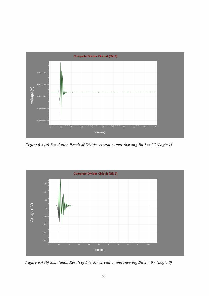
66
Figure 6.4 (a) Simulation Result of Divider circuit output showing Bit 3 ≈ 5V (Logic 1)
Figure 6.4 (b) Simulation Result of Divider circuit output showing Bit 2 ≈ 0V (Logic 0)
0 10 20 30 40 50 60 70 80 90 100
Time (ns)
4.99999985
4.99999990
4.99999995
5.00000000
5.00000005
Vo
ltag
e (
V)
Complete Divider Ciricuit (Bit 3)
0 10 20 30 40 50 60 70 80 90 100
Time (ns)
-200
-150
-100
-50
0
50
100
150
Vo
ltag
e (
nV
)
Complete Divider Ciricuit (Bit 2)

67
Figure 6.4 (c) Simulation Result of Divider circuit output showing Bit 1 ≈ 5V (Logic 5)
Figure 6.4 (d) Simulation Result of Divider circuit output showing Bit 0 ≈ 0V (Logic 0)
0 10 20 30 40 50 60 70 80 90 100
Time (ns)
4.99999985
4.99999990
4.99999995
5.00000000
5.00000005
Vo
ltag
e (
V)
Complete Divider Ciricuit (Bit 1)
0 10 20 30 40 50 60 70 80 90 100
Time (ns)
-200
-150
-100
-50
0
50
100
150
Vo
ltag
e (
nV
)
Complete Divider Ciricuit (Bit 0)

68
Thus,
From the Graphs it can be seen that the simulated results of a 4 bit output from the Divider
circuit= 1010.
This is true because 01100000111/00000101= 1010
Hence, the design of the complete Divider hardware is correct.

69
CHAPTER 7
CONCLUSION AND FUTURE WORK
7.1 Conclusion
This thesis proposed a simple but analytical approach for the design of a fuzzy logic
controller. The functional and logic design for an improved Fuzzy controller chip has been
described. The hardware requirements are quite modest and the entire design is performed
by using standard CMOS transistors. Also, the memory (ROM) modules required are of
minimal size and have been significantly reduced by using the symmetry of fuzzy rules and
fuzzy subsets. Uses of decimal point numbers are totally avoided and this has contributed a
lot for the massive reduction of the hardware and has also made the design simple.
Although this particular design controls only the Wash Time of a washing machine, the
design process can be extended to other control variables such as Water level and Spin
speed. The formulation and implementation of membership functions and rules will be
similar to the one described in this design.
Total number of transistors used in the overall design is 36,295 and the size of the complete
designed VLSI microchip is 30 mm2 using 0.5 µm CMOS technology.
7.2 Future Work
The design concept may be developed to output other necessary variables of the washing
machine such as water quantity, water flow speed, rinsing time and spinning time.
The design concept can be planned to expand further for the control of appliances and
devices other than washing machines.
70
REFERENCES
Han, H., Chun-Yi, S., & Yury, S. (2001). Adaptive Control of a Class of Nonlinear Systems with
Nonlinearly Parameterized Fuzzy Approximators. IEEE Transactions on Fuzzy Systems, Vol.9, No. 2 ,
315-323.
Hasan, S. R. (1994). Design of a pH controller ASIC Fuzzy logic chip for industrial application. Proc.
GlobalTRONICS Electronics Design Conference. Singapore.
Huandra, S. (2007). Patent No. 11,262,028. United States of America.
Ishibashi, O., & Hasegawa, H. (1991). Patent No. 5,241,845. United States of America.
Lee, Y. F., Lin, T.-C., Chen, C. C., & Tian, Y.-Z. (2008). Patent No. 12,241,568. United States of
America.
Lohani, P., & Hasan, S. R. (2009). Design of an improved controller microchip for washing machine.
16th Annual Electronic New Zealand Conference (pp. 20-26). Dunedin: Otago University Press.
Martin, K. (2000). Digital integrated circuit design. New York: Oxford University Press.
Mendel, J. (1995, April 30). Fuzzy Logic Systems for Engineering: A Tutorial. IEEE: Periodicals , pp.
345-375.
Michels, K., Klawonn, F., Kruse, R., & Nurnberger, A. (2005). Fuzzy Control. Berlin: Springer.
Murray, A., & Ho, E. (2006). New Motion Control Architecture Simplifies Washing Machine Motor
Control System Development. Industry Applications Conference (pp. 1229-1239). El Segundo, CA:
Conference Record of the 2006 IEEE.
Nakano, S., Shikamori, T., & Isao, H. (1991). Patent No. 5,230,228. United States of America.
Payne, T. R., Rice, S. A., & Wead, W. W. (1995). Patent No. 5,647,231. United States of America.
Reznik, L. (1997). Fuzzy Controllers. Oxford: Newnes.
Roberts, G. (1997). SPICE. New York: Oxford University Press.
Roberts, G. W. (1997). SPICE. New York: Oxford University Press.
Roth, C. H. (2004). Fundamentals of Logic Design. London: Brooks/Cole.
Workman, M. (1996). Hardware Requirements for Fuzzy Logic Control Systems. Lubbock, TX: Texas
Tech University.
Yonezawa, K., Takagi, Y., Iino, Y., & Nishimura, N. (2007). Patent No. 11,783,936. United States of
America.
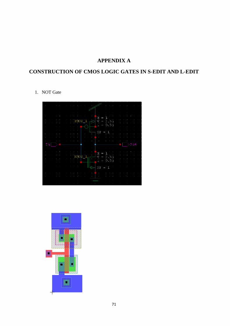
71
APPENDIX A
CONSTRUCTION OF CMOS LOGIC GATES IN S-EDIT AND L-EDIT
1. NOT Gate
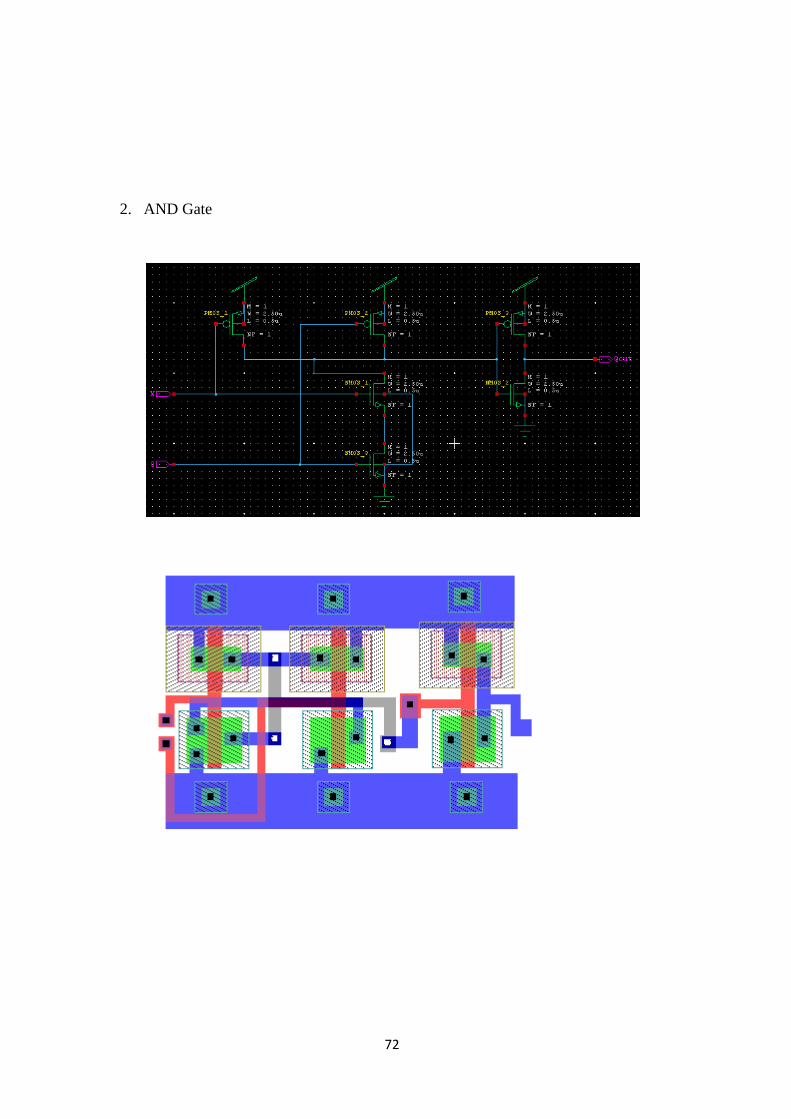
72
2. AND Gate

73
3. OR Gate

74
4. NAND

75
5. NOR
76
APPENDIX B
DESIGN OF OTHER BASIC COMPONENTS IN S-EDIT AND L-EDIT
1. Full Adder

77
2. Single D Flip-flop
78
3. Masked Programmable ROM for adjectives of LI: Small, Not Greasy and Light

79
4. Masked Programmable ROM for adjectives of LI: Medium
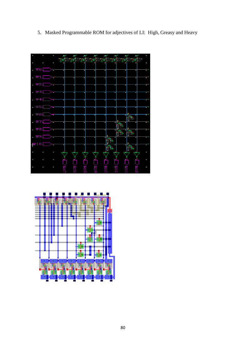
80
5. Masked Programmable ROM for adjectives of LI: High, Greasy and Heavy
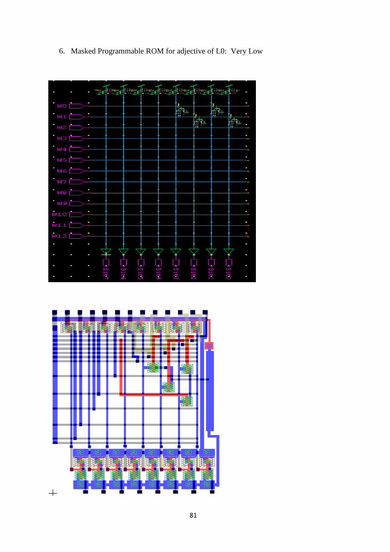
81
6. Masked Programmable ROM for adjective of L0: Very Low
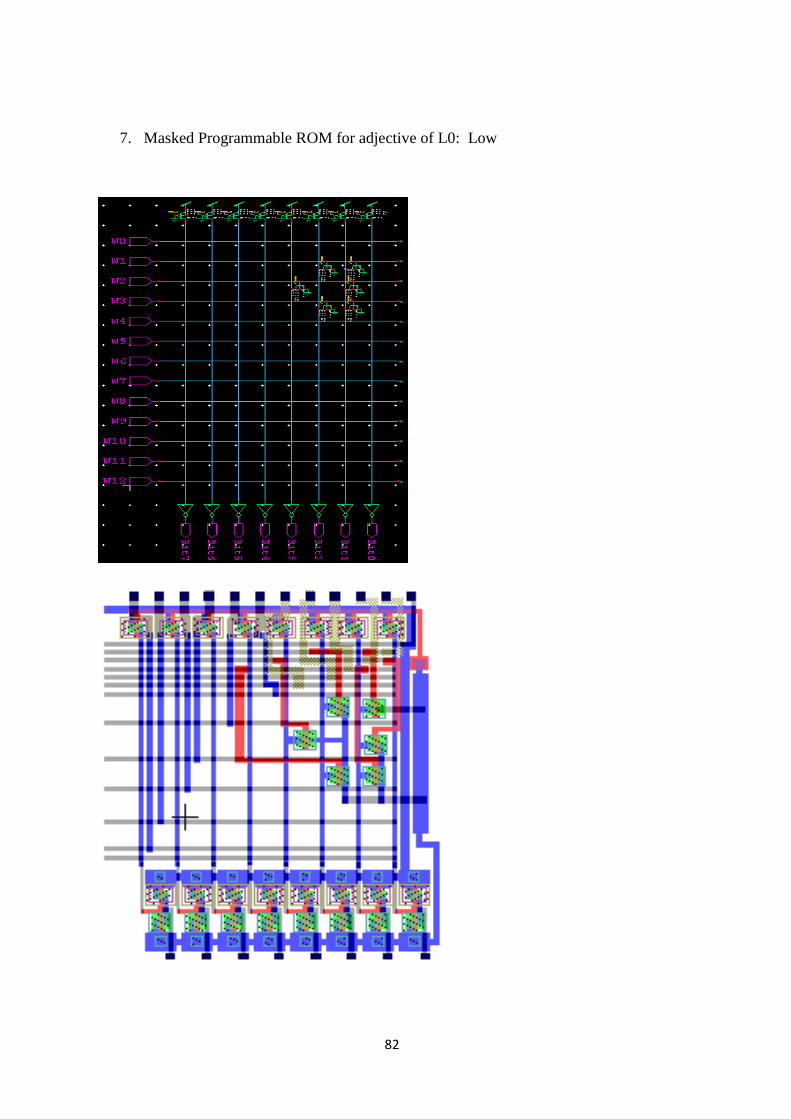
82
7. Masked Programmable ROM for adjective of L0: Low

83
8. Masked Programmable ROM for adjective of L0: Medium

84
9. Masked Programmable ROM for adjective of L0: High
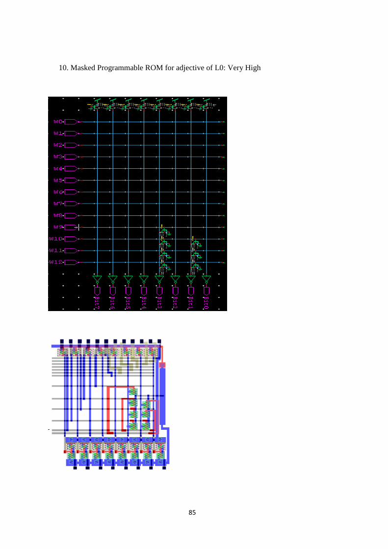
85
10. Masked Programmable ROM for adjective of L0: Very High