Embed Size (px)
Citation preview

Design of GaN-based microwave components and application to novel high power
reconfigurable antennas
By
Abdelaziz HAMDOUN
A thesis submitted to the Faculty of Graduate and
Postdoctoral Affairs in partial fulfillment of the requirements for the
degree of
Doctor of Philosophy
In
Electrical Engineering
Department of Electronics
Carleton University
Ottawa, Ontario, Canada
© October, 2016
Abdelaziz HAMDOUN

ii
Professor Mohamed HIMDI
University of Rennes 1, France,
Thesis Supervisor
Professor Langis ROY
Carleton University, Ottawa, Canada,
Thesis Supervisor
Professor Mustapha YAGOUB
University of Ottawa, Canada,
Referee
Professor Nathalie ROLLAND
University of Lille 1, France,
Referee
Adjunct Professor Olivier LAFOND
University of Rennes 1, France,
Examiner
Adjunct Professor Rony AMAYA
Carleton University, Ottawa, Canada,
Examiner
Adjunct Professor Steve McGARRY
Carleton University, Ottawa, Canada,
Examiner
Professor Barry SYRETT
Carleton University, Canada,
Thesis co-Supervisor
Professor Xavier CASTEL
University of Rennes 1, France,
Chair of Member Committee

Table of Contents
i
Table of Contents
Table of Contents .................................................................................... i
List of Figures ......................................................................................... i
List of tables ......................................................................................... vii
List of Acronyms .................................................................................. viii
Acknowledgements ............................................................................... ix
Abstract ................................................................................................. 1
Résumé en français ................................................................................ 2
CHAPTER I ............................................................................................ 1
Introduction ............................................................................................ 1
I. Research Motivations ........................................................................ 1
II. Objective of Research ...................................................................... 5
III. Thesis Organisation......................................................................... 6
CHAPTER II ........................................................................................... 7
A Review of the Literature of Gallium Nitride Technology .................... 7
I. Gallium Nitride Technology .............................................................. 7
1. Overview ........................................................................................ 7
2. Choice of the Substrate .............................................................. 14
II. NRC GaN500 MMIC HEMT Process Features and Limitations .... 16
III. Use of GaN in Reconfigurable RF/Microwave Systems .............. 21
IV. Summary ........................................................................................ 32
CHAPTER III ........................................................................................ 33
GaN Varactor and Switch Devices Modeling ........................................ 33
I. Introduction ...................................................................................... 33
II. GaN-based Varactors Diodes Modeling ........................................ 36
1. Review of GaN HEMT for Power Varactors Diodes Applications
.......................................................................................................................... 36

Table of Contents
ii
2. Realized GaN HEMT-based Varactor Diodes ............................ 46
3. GaN500v1 and GaN150v0 Varactor Devices ............................. 47
3.1 Small Signal Modeling ............................................................ 48
3.1.1 Analysis of Equivalent Capacitance ............................... 52
3.1.2 Analysis of Equivalent Series resistance ....................... 55
3.1.3 Analysis of Q-Factor ...................................................... 56
4. GaN500v2 Varactor Devices ...................................................... 58
4.1 Small Signal Measurement .................................................... 58
4.1.1 Analysis of Equivalent Capacitance ............................... 61
4.1.2 Analysis of Equivalent Series Resistance ...................... 65
4.2 Large Signal Measurements .................................................. 68
4.2.1 Analysis of Equivalent Capacitance ............................... 69
4.2.2 Analysis of Equivalent Series Resistance ...................... 71
5. Summary ...................................................................................... 74
III. GaN-based Switch Devices Modeling .......................................... 75
1. Review of GaN HEMT for Power Switching Devices Applications
.......................................................................................................................... 75
2. NRC GaN Switch Modeling ......................................................... 78
2.1 Proposed GaN Single Switch Model ..................................... 78
3. GaN500v2 Small Signal Switches Measurements ...................... 82
3.1 Different Sizes Standalone Signal Switch Devices ............... 82
3.2 SPST Switch Structure .......................................................... 87
3.3 SPDT Switch Structure .......................................................... 89
IV. Summary ........................................................................................ 92
CHAPTER IV ........................................................................................ 94
Realized GaN-Based Reconfigurable Circuits ...................................... 94

Table of Contents
iii
I. Introduction ...................................................................................... 94
II. Tunable Phase Shifters .................................................................. 97
1. Review ......................................................................................... 97
2. Design of Analog GaN-based Phase Shifter ............................ 105
2.1 Quadrature 3-dB 90° Hybrid Coupler ................................. 108
2.1.1. Simulated Results and Discussion ................................ 115
2.2 Phase Shifter Design ........................................................... 117
2.1.2. Simulated Results and Discussion ................................ 119
III. GaN Reconfigurable 3-dB/90° Hybrid Coupler .......................... 122
1. Review ....................................................................................... 122
2. Design of Reconfigurable 3-dB/90° Coupler ........................... 124
2.1 Simulated Results and Discussion ....................................... 125
IV. GaN-based Oscillator ................................................................. 129
1. Review ....................................................................................... 129
2. Design of GaN-based Oscillators ............................................. 132
2.1 Feedback Oscillator Topology ............................................ 133
2.2 Power Amplifier Design ....................................................... 133
2.2.1 PA Design Procedure .................................................... 133
2.2.2 PA Simulated Results .................................................... 139
2.2.3 PA Measured Results .................................................... 140
3. Oscillator Design ....................................................................... 142
3.1 Start-up Oscillation Condition ............................................. 142
3.2 Phase Noise in Oscillator .................................................... 144
3.3 Fixed Frequency Oscillator (FFO) ...................................... 145
3.3.1 Simulation Results ......................................................... 145
3.3.2 Measurements Results .................................................. 148
3.4 Tunable Frequency Oscillator (TFO) .................................. 149

Table of Contents
iv
3.4.1 Simulation Results ......................................................... 149
3.4.2 Measurement Results .................................................... 152
V. Frequency Reconfigurable Active Antennas ............................... 153
1. Review ....................................................................................... 153
2. Reconfigurable Annular Slot Antenna using GaN Varactor ..... 154
2.1 Antenna Design .................................................................... 154
2.2 Simulated Return Loss and Radiation Pattern .................... 155
2.3 Measured Return Loss and Radiation Pattern .................... 158
3. Reconfigurable Aperture Coupled Slot Antenna using GaN
Varactor ......................................................................................................... 162
3.1 Antenna Design .................................................................... 162
3.2 Simulated Return Loss and Radiation Pattern .................... 163
3.3 Measured Return Loss and Radiation Pattern .................... 167
4. Beam Steering Patch Antenna Arrays using GaN SPDT Switch
Structure......................................................................................................... 170
4.1 Antenna Design .................................................................... 170
4.2 Simulated Return Loss and Radiation Pattern .................... 174
4.3 Measured Return Loss and Radiation Pattern .................... 178
4.4 Measured Insertion Loss and Isolation of the Feeding System
.................................................................................................................... 181
4.4.1 Small Signal Measurements .......................................... 181
4.4.2 Large Signal Measurements ......................................... 184
VI. Summary ...................................................................................... 185
CHAPTER V ........................................................................................186
Conclusion and Future Work ...............................................................186
Bibliography ........................................................................................... 1

Table of Contents
ii


List of Figures
i
List of Figures
Figure II.1: Most used Semiconductor Technologies and their Frequency/Power limits [6] .................. 9
Figure II.2: Current due to trapping effect and thermal effect [18] ....................................................... 11
Figure II.3: A sketch of an AlGaN/ GaN HEMT structure with trapped electrons [19] ....................... 12
Figure II.4: Cross-Section of HEMTs (Not Drawn to Scale) ................................................................... 13
Figure II.5: Cross-sectional view of HFET, showing process sequence (not to scale) [31] .................... 19
Figure II.6: Photo of a T/R-Module front-end with GaN MMIC chips [43] ............................................ 22
Figure II.7: Measured output power versus frequency of the GaN MMIC DA at ................................. 23
Figure II.8: Measured power performance of the GaN MMIC HPA at 11 GHz .................................... 23
Figure II.9: Measured gain and noise figure versus frequency of the GaN MMIC ............................... 24
Figure II.10: (Left) A schematic view and (Right) a photograph of the Fabricated T/R module using
HTCC technology [44] ............................................................................................................................... 24
Figure II.11: Measured Pout of fabricated T/R module as a function of frequency, biased at 30 V [44]
.................................................................................................................................................................... 25
Figure II.12: Measured S-parameters of GaN LNA MMIC (Vds = 15 V) [44] ...................................... 25
Figure II.13: Photograph of the fabricated amplifier [45] ....................................................................... 26
Figure II.14: Measured PAE versus output power [45] .......................................................................... 26
Figure II.15: Measured gain versus output power [45] ........................................................................... 27
Figure II.16: The concept of impedance matching conditions of the band and class reconfigurable power
amplifier [46] .............................................................................................................................................. 28
Figure II.17: Photograph of the fabricated class-reconfigurable power amplifier [46] ......................... 28
Figure II.18: Simulated gain verses input power at different matching states [46] ............................. 28
Figure II.19: Simulated output power verses input power at different matching states [46] .............. 29
Figure II.20: Simulated power added efficiency verses input power at different matching states [46]
.................................................................................................................................................................... 29
Figure II.21: (Left) Top and cross sectional view and (Right) Picture of the packaged PA [47] .......... 30
Figure II.22: Acetone configuration: measurements at 2.3 GHz, simulations at 2. 4 GHz [47] ........... 30
Figure II.23: Air configuration: measurements at 5.7 GHz, simulations at 5.8 GHz [47] .................... 31
Figure III.1: Work Plan ............................................................................................................................. 35
Figure III.2: C-V characteristics of devices with different electrode length (spacing = 1 um, width = 50
um) [53] ...................................................................................................................................................... 37
Figure III.3: Extracted capacitance (black line) and resistance (white line) of the MSM varactor over
the entire bias range at 1.1 GHz. The inserted schematic shows the first-order equivalent circuit of the
MSM varactor [54] ..................................................................................................................................... 38

List of Figures
ii
Figure III.4: Q-factor versus tuning bias at 1.1 GHz [54] ....................................................................... 39
Figure III.5: A Schematic diagram of the AlGaN/GaN-based varactor [55] .......................................... 40
Figure III.6: Measured C-V curves of the untreated and sulfur-treated AlGaN/GaN-based MSM-2DEG
varactors [55] ............................................................................................................................................. 40
Figure III.7: Schematic diagram of the AlGaN/GaN MSM-2DEG varactor of the samples prepared in
this study [56] ............................................................................................................................................ 41
Figure III.8: Capacitance-Voltage (C-V) characteristics of varactors with different electrode areas (a)
without any dielectric film, (b) with SiO2 film, (c) with Gd2O3 film, and (d) with Si3N4 film.
Measurement frequency = 1MHz, electrode area = 37922, 85224, 151122, and 236472 μm2,
respectively [56] ......................................................................................................................................... 42
Figure III.9: Schematic Cross-sectional view of the GaN Schottky Varactor [57] ................................ 43
Figure III.10: C-V characteristics of the GaN Schottky Varactor [57]................................................... 43
Figure III.11: Schematic diagram of a GaN-based varactor and its layer structure [58] ..................... 44
Figure III.12: C–V curves measured for the samples with area of 5 × 10⁻⁵ cm2 at f = 1 MHz [58] .... 44
Figure III.13: Capacitance-voltage curves for (a) single diode structure and (b) two anti-parallel diode
structure [59] ............................................................................................................................................. 45
Figure III.14: Q factor versus reverse external bias for an anti-parallel varactor at f = 1 GHz, 2 GHz
and 3 GHz. Each diode has an area of 3.8×10⁻⁵ cm2 [59] ....................................................................... 46
Figure III.15: Schematic cross-section of HEMT, showing contacts and epitaxial structures, and
physical equivalent circuit origin at pinch-off (VG = -3.5 V) ................................................................... 47
Figure III.16: W40L500v1 Device in Microwave Probe Test .................................................................. 48
Figure III.17: Varactor equivalent circuit model ..................................................................................... 48
Figure III.18: Measured (lines) and Simulated (Dot) S11-parameter for G W40L0.5 .......................... 50
Figure III.19: Measured (lines) and Simulated (Dot) S11-parameter for W100L0.5 ............................ 50
Figure III.20: Measured (lines) and Simulated (Dot) S11-parameter for W50L0.15 ............................ 51
Figure III.21: Measured (lines) and Simulated (Dot) S11-parameter for W100L0.15 .......................... 51
Figure III.22: CEq versus frequency for the W40L0.5 device at VG =-3V ............................................... 52
Figure III.23: Extracted and Simulated CEq versus VG for GaN500v1 Devices .................................... 53
Figure III.24: Extracted and Simulated CEq versus VG for GaN150 Devices ........................................ 53
Figure III.25: Exctacted and Simulated REq versus VG at 2.5 GHz for GaN500v1 ............................... 55
Figure III.26: Extracted and Simulated REq versus VG at 2.5 GHz for GaN150v0 ............................... 55
Figure III.27: Extracted Q factor versus Frequency at VG = -3.5 V for GaN500v1 ............................... 57
Figure III.28: Extracted Q factor versus Frequency at VG = -3.5 V for GaN150v0 ............................... 57
Figure III.29: Measured (lines) and Simulated (Dot) S11-parameter for W50L0.5 .............................. 60
Figure III.30: Measured (lines) and Simulated (Dot) S11-parameter for G W100L0.5 ........................ 60

List of Figures
iii
Figure III.31: Measured (lines) and Simulated (Dot) S11-parameter for G W200L0.5 ........................ 61
Figure III.32: CEq versus frequency for the W50L0.5 device at VG =-3V .............................................. 62
Figure III.33: Extracted and Simulated CEq versus VG for W50L0.5 ..................................................... 63
Figure III.34: Extracted and Simulated CEq versus VG for W100L0.5 ................................................... 64
Figure III.35: Extracted and Simulated CEq versus VG for W200L0.5 ................................................... 64
Figure III.36: Extracted REq versus VG for GaN500v2 Devices .............................................................. 67
Figure III.37: Extracted (left) and Simulated (right) CEq versus VG for various power levels [-10, 18]
dBm for device W50L0.5 ........................................................................................................................... 70
Figure III.38: Extracted (left) and Simulated (right) CEq versus VG for various power levels [-10, 18]
dBm for device W100L0.5 ......................................................................................................................... 71
Figure III.39: Extracted (left) and Simulated (right) CEq versus VG for various power levels [-10, 18]
dBm for device W200L0.5 ......................................................................................................................... 71
Figure III.40: Extracted REq versus VG for various power levels [-10, 18] dBm for device W50L0.5 (left),
for W100L0.5 (middle) and for W200L0.5 (right) .................................................................................... 72
Figure III.41: Extracted Available (left) and reflected (right) RF Power versus Power from Source for
various DC Points for W50L0.5 ................................................................................................................ 73
Figure III.42: Extracted Delivered RF Power versus Power from Source for various DC Points for
W50L0.5 ..................................................................................................................................................... 73
Figure III.43: Simple Model for a HEMT in the switch configuration (a) ON-state and (b) OFF-state
mode............................................................................................................................................................ 76
Figure III.44: Linear model used to model the switching GaN HEMT transistors (4x40) [[90] .......... 80
Figure III.45: Equivalent Linear Circuit Model of GaAs FET Switch [91] ........................................... 81
Figure III.46: Schematic (left) of Common Gate Configuration standalone switch 2x200_GaN500v2
and Device in Microwave probes measurement setup (right) to Evaluate RF behavior ...................... 82
Figure III.47: Measured insertion loss of different transistor size in common gate, biased with VG=0V
(ON state) ................................................................................................................................................... 83
Figure III.48: Measured Isolation of different transistor size in common gate, biased with VG=-5V (OFF
state) ........................................................................................................................................................... 84
Figure III.49: Measured Return Loss (S11) of different transistor size in common gate, biased with
VG=0V (ON state) ....................................................................................................................................... 84
Figure III.50: Measured Return Loss (S11) of different transistor size in common gate, biased with
VG=-5V (OFF state) .................................................................................................................................... 85
Figure III.51: Linear model used to model the switching GaN HEMT transistors. ............................. 86
Figure III.52: Measured and Modeled Insertion Loss and Return Loss (S11) of switch 2x25 biased with
VG=0V (ON state) ....................................................................................................................................... 86

List of Figures
iv
Figure III.53: Measured and Modeled Isolation and Return Loss (S11) of switch 2x25 biased with VG=-
5V (OFF state) ........................................................................................................................................... 87
Figure III.54: Schematic (left) and Layout (right) of the Proposed SPST Switch Structure ................ 88
Figure III.55: Measured SPST performances .......................................................................................... 89
Figure III.56: Schematic (left) and Layout (right) of the Proposed SPDT Switch Structure ............... 90
Figure III.57: Measured and Modeled Return Loss, Isolation, and Insertion Loss of SPDT Switch
Structure .................................................................................................................................................... 91
Figure IV.1: (left) Tri-band system with three fixed duplexers and (right) with a single tunable
duplexer [96] .............................................................................................................................................. 95
Figure IV.2: Simplified RF front-end for a typical beamforming system in a non-GaN technology [[30]
.................................................................................................................................................................... 99
Figure IV.3: Example RF front-end possible with GaN with key components in blue [[30] ................ 99
Figure IV.4: Photograph of a novel GaN HEMT based high power high-pass/low-pass phase shifter
[99] ............................................................................................................................................................ 100
Figure IV.5: Measured insertion and return loss for high pass [99] .................................................... 101
Figure IV.6: Measured insertion and return loss for low pass [99] ...................................................... 101
Figure IV.7: Measured phase difference between the two states [99] ................................................. 101
Figure IV.8: Microphotograph of the 0°/22.5° GaN switched-filter phase shifter [100]...................... 102
Figure IV.9: Measured and simulated phase shift [100] ....................................................................... 103
Figure IV.10: Linearity measurement [100] .......................................................................................... 103
Figure IV.11: T-Phase shifter Circuit Configuration and microscope image [101] ............................. 104
Figure IV.12: Phase shift of the high-pass T-network and the corresponding inductance for 50 Ω
impedance matching [101] ...................................................................................................................... 104
Figure IV.13: phase shift of the T-Phase shifter in the frequency range of 32 GHz to 38 GHz [101] 105
Figure IV.14: Phase shifter based on 3-dB/90 branch-line hybrid coupler using distributed elements
.................................................................................................................................................................. 107
Figure IV.15: Phase shifter based on 3-dB/90 branch-line hybrid coupler using lumped elements . 107
Figure IV.16: Layout of a Spiral Inductor Generated from NRC GaN150 PDK [105]........................ 113
Figure IV.17: An Equivalent Circuit to Estimate LS, RS and Fres [105] ............................................ 113
Figure IV.18: Layout of A MIM Capacitor [105] .................................................................................... 113
Figure IV.19: Layout of the designed hybrid coupler ............................................................................ 114
Figure IV.20: 3-D Layout view of the designed hybrid coupler ............................................................ 115
Figure IV.21: Insertion Loss versus frequency ...................................................................................... 116
Figure IV.22: Return Loss versus frequency ......................................................................................... 116
Figure IV.23: Isolation versus frequency ............................................................................................... 116

List of Figures
v
Figure IV.24: Phase Shift Difference versus frequency ........................................................................ 117
Figure IV.25: Layout of the designed Phase Shifter ............................................................................. 118
Figure IV.26: 3-D Layout view of the designed Phase Shifter ............................................................. 118
Figure IV.27: Return Loss at several DC Bias from -3.5 V to -5.5 V ................................................... 121
Figure IV.28: Insertion Loss of the Phase Shifter at several DC Bias from -3.5 V to -5.5 V .............. 121
Figure IV.29: Phase Shift versus DC Bias at 10 GHz ........................................................................... 121
Figure IV.30: Layout of the designed hybrid coupler ............................................................................ 124
Figure IV.31: 3-D Layout view of the designed hybrid coupler ............................................................ 125
Figure IV.32: Return Loss at several DC Bias from -3.7 V to -4.8 V ................................................... 126
Figure IV.33: Isolation at several DC Bias from -3.7 V to -4.8 V ......................................................... 127
Figure IV.34: Level of S21 at several DC Bias from -3.7 V to -4.8 V ................................................... 127
Figure IV.35: Level of S31 at several DC Bias from -3.7 V to -4.8 V ................................................... 127
Figure IV.36: Phase Difference at several DC Bias from -3.7 V to -4.8 V ............................................ 128
Figure IV.37: Block diagram of a feedback oscillator ............................................................................ 129
Figure IV.38: Photo of the CGHV1J025D GaN Transistor Die ............................................................ 134
Figure IV.39: 3D Bond wire model. ........................................................................................................ 135
Figure IV.40: Simulated I-V Curves of the transistor ........................................................................... 137
Figure IV.41: K-factor and Delta ............................................................................................................ 137
Figure IV.42: A typical distributed bias network with radial stub ...................................................... 138
Figure IV.43: Fabricated PA under Test ................................................................................................ 139
Figure IV.44: Simulated Small Signal S-Parameters ........................................................................... 140
Figure IV.45: Measured Small Signal S-Parameters ............................................................................ 141
Figure IV.46: Ids of 260 mA at Vds of 18.6 V and Vgs of -2.5 V ........................................................... 142
Figure IV.47: Fixed Frequency Oscillator Fabricated Prototype ......................................................... 146
Figure IV.48: Small Signal Simulation Results (Open-Loop) ............................................................... 146
Figure IV.49: Harmonics Power Simulation of the FFO ....................................................................... 146
Figure IV.50: Pure Voltage Sinusoid at the Output of the FFO ........................................................... 147
Figure IV.51: Pure Current Sinusoid at the Output of the FFO .......................................................... 147
Figure IV.52: Simulated Phase Noise of the FFO ................................................................................. 147
Figure IV.53: Harmonics Power Measurement of the FFO .................................................................. 148
Figure IV.54: Tunable Frequency Oscillator fabricated Prototype ...................................................... 149
Figure IV.55: Oscillation frequency versus gate voltage ...................................................................... 150
Figure IV.56: Output power versus gate voltage at fundamental frequency ...................................... 151
Figure IV.57: Phase Noise versus gate voltage at 10 KHz, 100 KHz, and 1 MHz .............................. 151
Figure IV.58: Printed antenna prototype with GaN varactor load. ..................................................... 155

List of Figures
vi
Figure IV.59: Simulated return loss of the antenna alone ................................................................... 156
Figure IV.60 : Simulated antenna gain versus frequency .................................................................... 156
Figure IV.61 : Simulated normalized radiation pattern of the antenna at 11 GHz ............................ 157
Figure IV.62: Simulated return loss of the loaded antenna for different reverse-bias voltages ........ 158
Figure IV.63: Measured return loss of the loaded antenna for different reverse-bias voltages ......... 159
Figure IV.64 : Measured loaded antenna gain versus frequency for various DC bias ........................ 160
Figure IV.65 : Measured radiation pattern in H-plane of the loaded antenna under various DC bias
.................................................................................................................................................................. 160
Figure IV.66 : Measured radiation pattern in E-plane of the loaded antenna under various DC bias
.................................................................................................................................................................. 161
Figure IV.67 : (left) patch antenna (right) slot feeding loaded with GaN varactor ............................. 163
Figure IV.68 : Stuck-up whole antenna system structure .................................................................... 163
Figure IV.69 : Simulated return loss of the antenna alone .................................................................. 164
Figure IV.70 : Simulated antenna gain versus frequency .................................................................... 165
Figure IV.71 : Simulated normalized radiation pattern of the antenna at 11.35 GHz ....................... 165
Figure IV.72: Simulated reflection coefficient (S11) of the loaded antenna for different varactor
reverse-bias voltages ............................................................................................................................... 166
Figure IV.73: Measured return loss (S11) of the loaded antenna at no DC bias applied ................... 168
Figure IV.74 : Measured loaded antenna gain versus frequency at no bias DC applied .................... 169
Figure IV.75 : Measured normalized radiation pattern of the loaded antenna at 10.6 GHZ with no bias
DC applied ................................................................................................................................................ 169
Figure IV.76: 3D model of designed antenna system. ........................................................................... 171
Figure IV.77: Fabricated prototype of the antenna ............................................................................... 172
Figure IV.78: The feeding system including the three SPDT switch structures ................................. 172
Figure IV.79: Zoom on SPDT_1 switch .................................................................................................. 172
Figure IV.80: Zoom on the wires bonding connecting the SPDT_1 to The feeding system ................ 172
Figure IV.81: Front view of the fabricated antenna .............................................................................. 174
Figure IV.82: Simulated return loss of the antenna ............................................................................. 176
Figure IV.83: Simulated antenna gain versus frequency ..................................................................... 176
Figure IV.84: Simulated normalized H-plane at 2.43 GHz for four cases mentioned in Table IV.4 .. 177
Figure IV.85: Simulated normalized E-plane at 2.43 GHz ................................................................... 177
Figure IV.86: Measured return loss of the antenna .............................................................................. 179
Figure IV.87: Measured antenna gain versus frequency ...................................................................... 179
Figure IV.88: Measured normalized H plane at 2.43 GHz for four cases mentioned in Table IV.4 . 180
Figure IV.89: Measured normalized E plane at 2.43 GHz .................................................................... 180

List of tables
vii
Figure IV.90: Measured S-parameters for case_1 at Pin of 0 dBm ...................................................... 182
Figure IV.91: Measured S-parameters for case_2 at Pin of 0 dBm ...................................................... 182
Figure IV.92: Measured S-parameters for case_3 at Pin of 0 dBm ...................................................... 183
Figure IV.93: Measured S-parameters for case_4 at Pin of 0 dBm ...................................................... 183
Figure IV.94: Measured insertion loss versus input RF power for case_1 at 2.43 GHz ..................... 184
List of tables
Table II.1: Comparison between properties of the most commonly used semiconductor technologies [1]
.................................................................................................................................................................... 10
Table II.2: Parameters used in the selection of a grow substrate for GaN devices: lattice constant (α),
thermal conductivity at 300K (K300), thermal expansion coefficient (αL), wafer diameter and
approximate cost [30] ................................................................................................................................ 16
Table III.1: Presented GaN500v1 and GaN150v0 Devices Information ................................................ 47
Table III.2: Parameters values of the equivalent circuit ........................................................................ 49
Table III.3: Comparison of capacitance performances between GaN500 and GaN150 ........................ 58
Table III.4 : Presented GaN500v2 Devices Information ......................................................................... 58
Table III.5: Parameters values of the equivalent circuit ........................................................................ 59
Table III.6: Model Circuit Parameters Values ........................................................................................ 67
Table III.7: Model Circuit Parameters Values ........................................................................................ 85
Table III.8: Performances of the SPDT at the Marker m4 ..................................................................... 91
Table IV.1: Optimized Values of Inductors L1 and L2 .......................................................................... 112
Table IV.2: Optimized Values of Capacitors C1 and C2 ....................................................................... 112
Table IV.3: Dimensions of Stubs............................................................................................................. 139
Table IV.4: Predicted different impedances of the SPDT ports. ........................................................... 173
Table IV.5: Switching configuration to achieve radiation pattern reconfigurability. ......................... 174

List of Acronyms
viii
List of Acronyms
GaN Galium Nitride
AlGaN aluminum gallium nitride
GaAs Galium Arsenide
SiC silicon carbide
Si silicon
InP indium phosphide
SoP System-on-Package
FET Field-effect transistor
HEMT High Electron Mobility Transistors
2DEG two-dimensional electron gas
HBT Heterojunction bipolar transistor
HEMT High electron mobility transistor
HVPE Hydride vapour phase epitaxy
LNA Low-noise amplifier
PA Power Amplifier
MBE Molecular beam epitaxy
MEMS Micro-electromechanical systems
MIM Metal-insulator-metal
MMIC Monolithic microwave integrated circuit
MOCVD Metal-organic chemical vapour deposition
NRC National Research Council Canada
PCB Printed circuit board
RF Radiofrequency
SPDT Single-pole-double-throw
SPST Single-pole-single-throw
AIA Active Integrated Antennas

Acknowledgements
ix
Acknowledgements
لله الحمد (Alhamdulillah)
Seldom anything is achieved without help, support, guidance,
encouragement, love and care of other people. I am fortunate to have such people
around me who have made my journey during my doctoral studies fruitful, rewarding
and enjoyable.
Firstly, I am particularly indebted to my supervisors Pr. Mohammed
HIMDI from University of Rennes 1 and Pr. Langis ROY from Carleton University,
and my co-supervisor, Dr. Olivier LAFOND from University of Rennes 1, for the
unconditional support, valuable guidance and endless patience they generously
provided during my thesis research. I must also note the financial support of my
advisors. I graciously thank Pr. Barry Syrett for accepting to be my co-supervisor at
Carleton University for the last year. I am also grateful to Pr. Rony AMAYA and Pr.
Garry TARR for their useful advice when I start dealing with GaN HEMT devices.
I am also grateful to Dr. Ibrahim HAROUN from NRC for giving me the
opportunity to get the possibility of an internship in NRC and to work side by side
with the NRC GaN group team. I have gained valuable insight into the GaN
technology.
I graciously thank Pr. Steve McGARRY, Pr. Mustapha YAGOUB for
accepting to be a part of my PhD thesis committee members.
I wish to express my sincere thanks to all staff of Laboratory IETR and the
department of electronics at Carleton University, for providing me with all the
necessary facilities for the research. Special thanks go to Blazenka POWER, Anna
LEE and Mikhail NAGUI from Carleton University, and also Noelle LE BER from
University of Rennes 1 for their previous helps.

Acknowledgements
x
Also, special thanks are reserved for fellow colleagues Tyler Ross, Nathan
Jess, Shiecheng YANG and Alexis MARTIN, who continue to set an example for
graduate students with their thirst for knowledge and enthusiasm to share it.
On a personal note, I would like to express my sincerest gratitude to my
brother Bouchaib and his wife, Bouchra, for their financial and moral support since I
came to France for study. I would also like to express my deepest gratitude to my
parents, brothers, and sisters (meaning also nieces) for the continuous
encouragement which helped me endure tough moments. My gratitude also goes to
my friends in Rennes and Ottawa, who encouraged me when needed. The name of
best friends in particular should be highlighted. Tarik DANKIR for his
encouragements and moral support and Imad ABDELJAOUAD who has been an
inspiration and example for me since I first moved to Canada for my PhD degree.
Last but certainly not least, my future wife Imane EL ABBOUDY, whose
love, understanding, and patience gave me the confidence and strength I needed to
achieve success.
Abdelaziz HAMDOUN
October, 2016
O Allah, benefit me by that which You have taught me, and teach
me that which will benefit me, and increase me in knowledge.
هم انفعني بما عل متني وعلمني ما الل
ينفعني وزدني علما

Abstract
1
Abstract
This thesis demonstrates the feasibility of using gallium nitride (GaN)
technology in reconfigurable RF systems. GaN-based varactor diodes and switch
circuits are pursued as promising candidates for high-power/high-frequency
applications. The first part is devoted to active GaN device development. Active
components were realized using the Canadian National Research Council (NRC) GaN
HEMTs process. Based on three process, such as, GaN150v0 (gate length of 0.15um),
GaN500v1 and GaN500v2 (both with gate length of 0.5um), many varactor diodes
with size different have been manufactured and characterized via DC and RF small-
signal and large-signal measurements. Then, the varactor diodes were modeled by
analytic equations containing empirical coefficients. These expressions have been
introduced for the first time for the voltage dependency of equivalent capacitance
(CEq) and series resistance (REq) and can be used as a general model to represent the
nonlinear behavior of GaN based varactors. For small-signal operation, all of the
developed equations describing REq and CEq are only bias voltage and device geometry
dependent, while for large-signal operation, the influence of RF-power must be taken
into account. In addition, different size single stand-alone switches were fabricated
using GaN500v2. By analyzing the small-signal measurements, it was observed that
the isolation is high at low frequencies but quickly drops with increasing frequency.
Also, it was observed that the larger the device the lower the insertion loss and the
poorer the isolation will be. Moreover, based on these small-signal measurements, a
model was introduced.
The second part addresses the integration and design aspects of the
reconfigurable proposed circuits, such as tunable phase shifter, reconfigurable 3-dB
90° hybrid coupler, tunable frequency oscillator, beam switching antenna array and
matching reconfigurable patch antenna operating below 10 GHz. Here the developed
GaN varactors and switches are used for achieving the tenability purpose.

Résumé en français
2
Résumé en français
Cette thèse a pour objectif de démontrer la faisabilité de l'utilisation de la
technologie Nitrure de Gallium (GaN) dans les systèmes RF / micro-ondes
reconfigurables. La technologie GaN doit permettre de supporter des puissances
élevées avec un rendement important. Le GaN qui présente une large bande interdite
possède des propriétés physiques lui permettant d’être largement utilisé pour la
conception de circuits actifs à forte puissance. En effet, ses qualités intrinsèques,
champs de claquage élevé, forte conductivité thermique, forte densité d’électrons, et
bonne vitesse de saturation, lui confèrent de très bonnes performances aux hautes
fréquences que ce soit pour les applications de puissance ou faible bruit. La
technologie GaN est donc un candidat très prometteur pour la réalisation de fonctions
hyperfréquence haute puissance/haute fréquence, telles que les amplificateurs de
puissance, les mélangeurs, les oscillateurs contrôlés en tension (VCO) ou encore les
amplificateurs faible bruit (LNA).
Cependant, malgré les caractéristiques intéressantes des dispositifs GaN,
il reste encore des défis de fabrication à relever avant que cette technologie ne soit
largement adoptée à l'avenir. Ces défis sont liés à deux aspects, le premier
technologique et le second commercial. Technologiquement, les dispositifs HEMTs
basés sur le GaN sont affectés par deux phénomènes importants, à savoir l'effet de
piégeage et l’effet thermique (ou auto-échauffement des dispositifs) qui peuvent
directement causer la dispersion du courant. Commercialement, un inconvénient de
la technologie GaN concerne le coût de fabrication des composants. La réduction du
coût de production est un facteur important pour pouvoir largement commercialiser
les dispositifs GaN. De plus, le peu de disponibilité de matière GaN conduit à
épitaxier le GaN sur des substrats tels que Silicium (Si), Carbure de Silicium (SiC) et
le Saphir, ce qui peut dégrader les caractéristiques des composants GaN. Ces aspects
sont abordés dans le chapitre II de ce manuscrit.

Résumé en français
3
Les travaux de thèse s’inscrivent dans une stratégie de développement des
dispositifs GaN nécessaires à la conception de circuits RF reconfigurables. Les
travaux sont divisés en deux parties principales. La première partie de ce travail de
thèse est consacrée au développement et à la caractérisation des circuits actifs
réalisés à base de la technologie GaN. Pour cela une investigation approfondie autour
de diodes Varicap et de commutateurs a été menée et présentée. Les composants
actifs ont été réalisés en utilisant le processus de fabrication GaN HEMTs offert par
le Conseil National de Recherches du Canada (CNRC). Pour ce faire, trois processus
GaN HEMT : le GaN150v0 avec une longueur de grille de 0,15 um, le GaN500v1 avec
longueur de grille de 0,5 um et le GaN500v2, ont été investigués pour fabriquer des
diodes varicap avec des tailles différentes. Ces diodes ont ensuite été caractérisées en
DC, en petits et grands signaux RF jusqu'à 20 GHz. Ici, les diodes varicap sont
réalisées simplement en reliant le drain à la source, conduisant à réaliser une jonction
Schottky qui peut être considérée comme « Planar Schottky Varactor Diode (PSVD)
». La tension VG de polarisation est alors appliquée entre le drain/source et la grille.
En outre, ce type de diode ne nécessite aucun changement particulier des couches
épitaxiales du procédé de fabrication HEMTs. Ensuite, les diodes varicap ont été
modélisées en petit et grand signal par des équations analytiques. Ces expressions
ont été introduites pour décrire la variation de la capacité équivalente (CEq) et la
résistance série (REq) en fonction la tension DC appliquée sur le composant. Ces
équations peuvent être utilisées comme un modèle général pour représenter le
comportement non-linéaire des diodes varicap basées sur la technologie GaN. Pour le
modèle petit signal, les équations analytiques développées ne sont dépendantes que
de la tension de polarisation appliquée sur le dispositif et de la géométrie de la diode,
tandis que pour le modèle grand signal, l'influence de la puissance RF a aussi été
prise en compte pour décrire le comportement de REq et CEq. Pour étendre l’étude
autour des composants GaN actifs utilisés dans les systèmes RF reconfigurables,
plusieurs commutateurs avec différentes tailles configurés en grille commune ainsi
que des structures de commutateurs tels que le SPST (Single Pole Single Throw) et

Résumé en français
4
le SPDT (Single Pole Double Throw) ont été fabriqués, en utilisant le processus de
fabrication GaN500v2. En analysant les mesures en petit signal des commutateurs
simples, on a pu observer que l'isolement est bon aux basses fréquences, mais se
dégrade rapidement avec l'augmentation de celle-ci. En outre, on a pu conclure que
plus le dispositif est grand, plus les pertes d'insertion s’améliorent, alors que
l’isolation se dégrade. Donc un compromis entre perte d'insertion et isolation a été
fait pour choisir les transistors individuels qui ont par la suite été utilisés pour la
conception des structures de commutateurs plus complexes (SPST et SPDT). De plus,
en se basant sur ces mesures petit signal, un modèle circuit a été introduit.
La deuxième partie de ces recherches de thèse aborde les aspects de l'intégration de
ces dispositif actifs GaN (diodes varactor et commutateurs) et de la conception de
circuits reconfigurables proposés, tels qu’un déphaseur reconfigurable, un coupleur
(3dB, 90°) reconfigurable, un oscillateur accordable en fréquence, ainsi qu’un réseau
d’antennes à commutation de faisceau et une antenne unitaire accordable en
fréquence. Initialement, un nouveau RUN technologique devait nous permettre de
concevoir de nouveaux designs complètement intégrés en technologie GaN
notamment le déphaseur et le coupleur (3dB, 90°) reconfigurable en fréquence mais
malheureusement ce RUN technologique n’ayant pas été assuré, il a donc été décidé
d’utiliser les diodes varactors et les commutateurs préalablement fabriqués et testés
sous pointe. Ceci a engendré des soucis puisque ces puces étaient de très petites
dimensions et donc difficilement découpables puis intégrables dans les circuits
imprimés tels que l’oscillateur ou les antennes. Toutefois, dans un souci de mener
jusqu’au bout cette étude et de réaliser les circuits et antennes reconfigurables, de
gros efforts ont été consentis afin de récupérer des diodes et commutateurs sur les
wafers de base. Il a donc pu être possible de réaliser l’oscillateur et les deux types
d’antennes reconfigurables. Si l’oscillateur contrôlé en tension et reconfigurable grâce
à une diode Varicap préalablement fabriquée et caractérisée n’a pu aboutir à des
résultats expérimentaux concluants, les prototypes d’antenne élémentaire
reconfigurable en fréquence ou en diagramme à l’aide d’un réseau d’antennes

Résumé en français
5
commutable ont permis de démontrer la faisabilité de tels concepts en utilisant des
composants actifs en technologie GaN.


Introduction
1
Chapter I
---------------------------------------------------------------------------------------------------------------------
Introduction
I. Research Motivations
Nowadays, people are living in a society in which processing, flow and
exchange of information are vital for their existence. Connectivity and mobility are
two major issues in such society, which are related to the flow and exchange of
information. On one hand, portable devices with internet provide connectivity which
allows communication as well as access to information. On the other hand, wireless
technologies bring mobility. People can move and still be able to communicate while
having access to various kinds of information. This is the reason why radio frequency
(RF)/microwave systems have evolved to integrated formats. This approach is called
system-on-package (SoP), where many technologies are mixed in one package
allowing increased simultaneous functionalities. Furthermore, the recent trend in
RF/microwave technology is toward circuits that are highly miniaturized integrated

Research Motivations
2
and reliable, with low power consumption, and reduced cost. Monolithic Microwave
Integrated Circuits (MMICs), based on semiconductor technology, are one of the keys
to meeting the requirements of this technology mixing. Additionally, most MMICs
currently in production, such as gallium arsenide (GaAs), silicon carbide (SiC), silicon
(Si), indium phosphide (InP), etc, operate in the microwave and millimeter-wave
(mm-w) range with modest breakdown voltages and limited power handling
capabilities. But there are increasing applications in the RF/microwave spectrum
where higher power/frequency is required.
Over the past decade, several changes have drawn more attention to
RF/microwaves power devices. Increasing demands of high power handling
capabilities and worries about capabilities of functioning in harsh environments have
created a need for alternatives to traditional semiconductors technology. Due to its
high critical breakdown field associated with wide band gap energy as well as its high
saturated electron velocity, gallium nitride (GaN) is a potential solution to satisfy
these simultaneous requirements for RF, microwave and mm-w transmitters for
communications and RADAR [1]. On one hand, GaN-based high electron mobility
transistors (HEMTs) power devices are considered as an excellent candidate for
future power devices due to its high breakdown voltage and high saturation drain
current [1]. On the other hand, besides being used for high power purposes, GaN
HFETs devices are also a strong candidate to be used in harsh environment receiver
applications due to the robust nature and good low noise performance of these devices
[2], where others semiconductors can suffer.
With the advent of this wide band gap material, enormous progress has
been made until now especially in the development of GaN technology. Consequently,
more and more industries and academic research labs in the field of semiconductors
have introduced different GaN HEMTs processes (i.e United Monolithic
Semiconductors (UMS), TriQuint, Cree, NRC (National Research Council Canada),
etc). These devices are intended to fulfill the growing demands for high power at high

Introduction
3
frequency electronic components as well as for high voltage power switches operating
at higher frequencies. Furthermore, GaN HEMTs based MMIC technology is now
challenging the other traditional semiconductor technologies such as GaAs mostly by
offering the highest level of integration and the smallest form factor while keeping to
operate with high voltage and to handle high power levels.
However, some challenges remain with GaN technology. The most serious
problem is the cost of a GaN substrate in which the power devices are fabricated and
the pace of maturation of their technological processes. Another issue is the lack of
bulk GaN source material which leading to the need for GaN growth by using
mismatched substrates such as Si, SiC and sapphire.
The recent trend in RF/microwaves technology is toward circuits that are
highly reconfigurable compacted and reliable with more functionalities, with low
power consumption, and reduced cost. In particular, the downsizing demands in
RF/microwaves wireless communication systems are growing exponentially as the
number of multi-band and multi-service systems has increased along with the need
for high power handling capabilities at higher frequency. The tunable and
reconfigurability aspect of modern RF/microwaves front-ends transceivers (Tx/Rx) is
also an interesting subject concerning GaN HEMTs technology. Research into the
usage of GaN based high power RF switches and varactors provide further
opportunities for GaN to achieve these demands.
GaN technology is emerging as a major promising candidate for
reconfigurable high power circuits for RF front-end Tx/Rx. Moreover, there is a wide
consensus that the antenna system should be integrated in the same package with
the front-end integrated circuit [3]. As an example, mobile communications (including
SATCOM) imply that reconfigurable radiation pattern antennas are now of interest
for such applications to steer the antenna beam. So antenna array system with a
controlled gain and phase between single elements are often considered. In
particular, for mobile applications, the antenna array must exhibit the capability to

Research Motivations
4
align its beam in the direction of the strongest signal. Hence, an antenna array with
beam-steering capability is imperative and could be integrated on the same package
with its two crucial components, phase shifter and gain amplifier to produce the
desired amplitude and phase.
Fulfilling the in-depth development of GaN HEMTs technology for tunable
high power circuits, it has become the motivation of this research to investigate novel
highly compact reconfigurable active microwave circuits operating up to X-band
frequency by using developed GaN varactor and switch models.
The main aim of this thesis research is to investigate and characterize
GaN-based varactor diodes and switches that will be integrated to realize
reconfigurable RF/microwave circuits operating up to X-band frequency. This band of
frequency from 8 GHz to12 GHz is primarily used for military communications and
Wideband Global SATCOM systems. It is mostly used in radar applications including
continuous-wave, pulsed, single-polarization, dual-polarization, synthetic aperture
radar and phased arrays. X-band radar frequency sub-bands are used in civil,
military and government institutions for weather monitoring, air traffic control,
maritime vessel traffic control, defense tracking and vehicle speed detection for law
enforcement. This band is less susceptible to rain fade than the Ku Band due to the
lower frequency range, resulting in a higher performance level under adverse
weather conditions.
This thesis research has been conducted as a collaboration between
University of Rennes 1 through “l’Institut d’Electronique et de Télécommunications
de Rennes (IETR)”, and Carleton University through the “Department of Electronics
(DOE)”. This collaboration is created from the PhD cotutelle (joint) program offered
by both institutions. DOE has the expertise in CAD for electronic circuit design, RF
and microwave circuits, photonics and integrated circuit using semiconductor
technologies including GaN technology. A group of researchers from Carleton
University is deeply involved in developing of circuits based on GaN technology.

Introduction
5
These researchers have a good relationship with the National Research Council
(NRC) which provides GaN HEMTs foundry facilities, via CMC, and are involvedwith
NRC’s GaN team to develop this novel semiconductor technology. As a result,
students as well as researchers from Carleton University can get access to this
foundry. On the other hand, IETR is one of the largest and most research intensive
labs in the design and characterization of active antennas up to millimeter-wave
bands. Moreover, IETR provides facilities allowing the design of antennas, such as,
EM simulators (i.e. CST, HFSS, etc.), unique measurement facilities in France
including network analyrers up to 110 GHz for S-parameter measurements, and an
anechoic chamber working up to 110 GHz for measuring radiation patterns of
antennas.
II. Objective of Research
The proposed overall objective of this research is to study reconfigurable
integrated microwave circuits using developed GaN varactor and switch models for
use, for example, in X-band systems. It is expected that this project will demonstrate
a new concept of realizing reconfigurable large-signal microwave circuits based on
GaN technology, which will be used for the first time as active varactors and switches
co-integrated in low cost microstrip technology to achieve the tunability of circuits.
The proposed specifics objectives are:
1. Explore possibilities of emerging GaN technology for integrated circuits that
are miniaturized such as phase shifter and frequency reconfigurable hybrid
couplers where the control functionality is achieved by using varactor diodes.
2. Investigate possibilities for RF reconfigurable circuits using active GaN
components with a low-cost substrate. For this a reconfigurable oscillator, a
beam switching antenna array and a matching reconfigurable patch antenna
operating below 10 GHz were designed.

Thesis Organisation
6
3. Demonstrate a working prototype that combines active GaN devices and
passive components so as to experimentally validate the proposed concepts.
It will be shown that the developed GaN varactor and switch models can
be used along with passive circuit designs in low cost microstrip technology so as to
achieve, in the same circuit, reconfigurability and good RF performance. Additionally,
this research project will demonstrate the great potential of GaN for use in other
tunable microwave high power applications such as oscillators and reconfigurable
antennas.
III. Thesis Organisation
The thesis begins with the chapter II dealing with a review of gallium
nitride technology. Then, chapter III presents the characterization and modeling of
gallium nitride varactor and switch devices manufactured with NRC process. The
final chapter IV covers contributions and realized applications over this thesis
research.

A Review of the Literature of Gallium Nitride Technology
7
Chapter II
---------------------------------------------------------------------------------------------------------------------
A Review of the Literature of Gallium
Nitride Technology
I. Gallium Nitride Technology
1. Overview
Since gallium nitride (GaN) is used as a semiconductor technology to
design the circuits for this thesis, it is necessary to review the characteristics of this
technology and make a brief comparison with commonly used semiconductor
technologies. GaN technology has been and still getting more and more attention for
RF/microwave systems that require high power handling capabilities and low noise
figure. This sets the field of GaN electronics in motion, and today the technology is
improving the performance of several applications including, mobile communication,

Gallium Nitride Technology
8
wireless base stations, communication and military radar systems, where its focus is
shifting to further advantages such as high efficiency as well as the reduction of
worldwide energy consumption [4].
Historically, development of semiconductor technologies based on
Monolithic Microwave Integrated Circuit (MMIC) has always advanced to more and
more performance improvements in terms of more high power handling capabilities,
more gain, high efficiency, high linearity, decreasing noise figure [2]-[5]. In the early
1990s, GaN was revealed as a potential solution to satisfy the simultaneous
requirements of high frequency and power [1]. GaN material has the capability of
satisfying system device requirements from low-frequencies [7]-[8] through
millimeter-waves [9]-[10]-[11]-[12] and was deemed an excellent material for being
useful in high power applications. Because of its special properties, GaN technology
is truly recognized as a revolutionary wide band gap technology resulting in dramatic
afforded power levels that exceed many times (> 5 times) those levels achieved with
other traditional technologies such as, indium phosphide (InP), gallium arsenide
(GaAs), and silicon (Si). As a result, current densities in excess of 2 A/mm have been
reported [13]-[14]. High power densities of 40 W/mm have also been reported at 4 GHz
with 1.2 A/mm by Cree using field-plated devices [15]. Watt-level output power has
been demonstrated and reported at W-band in [9]-[10]-[11] by HRL, Raytheon and
Fujitsu. In [12] Cree has demonstrated power density higher than 25 W/mm of gate
periphery with unity current gain frequencies, Ft, greater than 40 GHz reported. As
a brief comparison, Figure II.1 recapitulates the most used semiconductor
technologies and their limits in terms of power handling capability and operating
frequency.

A Review of the Literature of Gallium Nitride Technology
9
Figure II.1: Most used Semiconductor Technologies and their Frequency/Power
limits [6]
GaN offers very high breakdown field, high electron mobility, and
saturation velocity. It is also known that GaN has an excellent thermal conductivity
and ability to operate at high temperatures which make it an ideal candidate for high-
power and high-temperature microwave applications [1]. Moreover, GaN is a great
candidate to enable the development of next generation of wireless and satellite
communication systems that are needed to meet emerging demands for high data
throughput, energy efficient wireless systems, reduced carbon footprints of wireless
networks, high power electronic solutions for smart and efficient applications, and
interoperability among diverse communication standards. Today, gallium nitride
high electron mobility transistors (HEMTs) or heterojunction FETs (HFETs) are the
most advanced electronic nitride devices. The hetero-structures offer many
advantages such as high breakdown and transport properties of un-doped GaN.

Gallium Nitride Technology
10
As shown in Table II.1, a comparison between the electrical/physical
properties of the commonly used semiconductor technologies is illustrated. GaN has
high sheet carrier density and channel charge density, which produce high output
power. Also it has high electron mobility, which is largely responsible for low on-
resistance, and therefore, high power added efficiency could be achieved at higher
frequencies. As a result, GaN HEMTs devices can achieve much higher breakdown
voltage than the other technologies, very high current density, and sustain very high
channel operation temperature. For comparison purposes, TriQuint’s 0.25μm GaAs
process has a typical breakdown voltage of 15V [16] while TriQuint’s 0.25μm GaN
process has a typical breakdown voltage of 100V [17]. Additionally, the combination
of significant electron mobility and a good saturation velocity enable high speed
operation of active devices. As a matter of fact, GaN circuits demonstrate their
capabilities of operating adequately at high frequencies.
All of these presented factors indirectly improve the efficiency of GaN
devices. Furthermore, possible epitaxial growth on SiC substrate, which has excellent
thermal properties, makes this device optimal to operate at high power. Later in this
chapter, the possibility of growing GaN over other substrates will be more detailed.
Table II.1: Comparison between properties of the most commonly used
semiconductor technologies [1]
Semiconductor (Typical Materials) Si GaAs InP SiC GaN
Characteristic Unit
Bandgap eV 1.1 1.42 1.35 3.25 3.49
Electronic Mobility at 300 ºK cm2/V.s 1500 8500 5400 700 1000-2000
Saturated Electronic Velocity x107 cm/s 1 1.3 1 2 2.5
Critical Breakdown Field MV/cm 0.3 0.4 0.5 3 3.3
Thermal Conductivity w/cm.k 1.5 0.5 0.7 4.5 >1.5
Charge channel Density x1013/cm2 0.3 0.2 1
Resistivity Ω.cm 1.5 1x10⁷ 1x10⁵
Relative Dielectric Constant Ԑr 11.5 12.8 12.5 10 9
Loss tangent (at 10 GHz) Tg 0.015 0.0004 0.003

A Review of the Literature of Gallium Nitride Technology
11
However, despite the superior characteristics of GaN device, there still
remain some issues at multiple levels with respect to fabrication (process, device,
circuit and system) that must be overcome before being widely adopted in future.
These challenges that are impacting the development of GaN technology can be
summarized in two main challenges such as technological (device processing) and
commercial tasks.
The first technological (device processing) challenge is that the GaN
HEMTs are affected by two important phenomena, namely the trapping effect and
thermal effect (or self-heating), which can directly cause current dispersion such as
collapse and rolling off as shown in Figure II.2. This existence, of dispersion effects
observed in GaN devices, acts to restrict the drain current and voltage excursions,
thereby limiting the initial expectations of device’s performances in term of high
power and high frequency.
Figure II.2: Current due to trapping effect and thermal effect [18]

Gallium Nitride Technology
12
Current collapse is explained as a transient and recoverable reduction in
drain current response caused by trapping effects. In general, this phenomena means
that some electrons are captured by traps somewhere in AlGaN/GaN HEMTs hetero-
structures [18] as shown in Figure II.3. These captured electrons reduce the sheet
electron density in the channel, leading to increase dynamic Ron leading to drain
current dispersion [19]. In principle, electron trapping can occur at different locations
such as metal/AlGaN interface, the un-gated AlGaN surface near the gate edge,
AlGaN/GaN interface, and the buffer GaN layer during HEMT operation.
Figure II.3: A sketch of an AlGaN/ GaN HEMT structure with trapped electrons [19]
Most reported works, explaining this effect, conclude that trapping effect
can mainly reside at the surface [20]-[21], in the AlGaN barrier layer, at the two-
dimensional electron gas (2DEG) interface, and in the GaN buffer layer [22]-[23]. This
effect is produced when a large bias voltage is applied between the source and drain,
which induces a quick acceleration of the electrons in the conducting channel. These
fast random moving electrons can be injected into an adjacent region of the device
structure and became trapped if this region contains a significant concentration of
traps which is the case for the GaN buffer layer.
On the other hand, thermal and self-heating effects exist in every power
semiconductor device. Especially when the device is working in the high voltage and
high power region, the self-heating causes electron carriers to accelerate in random
directions instead of following the drain to source channel. Some of the electrons eject

A Review of the Literature of Gallium Nitride Technology
13
themselves out of the channel, causing significant roll off in the high voltage and high
current region, which is observed in DC current variations, as shown in Figure II.2.
The simplified vertical semiconductor structure of a GaN/AlGaN HEMTs
is illustrated Figure II.4.
Figure II.4: Cross-Section of HEMTs (Not Drawn to Scale)
Barrier: This semiconductor layer isolates the gate and the channel so that
very low current flows between the channel and the gate. In GaN FETs, the
barrier is typically made of aluminum gallium nitride (AlGaN).
Channel: The channel or 2-DEG is the region where electrons flow from the
source to the drain. The channel is typically made of high-quality GaN.
Buffer: The role of the buffer is to restrict the movement of the electrons within
the channel. In other words, the buffer acts as a barrier that prevents the
electrons from wandering into the substrate. In a GaN FET, the buffer is
typically made of GaN doped with carbon (C) or iron (Fe).
Nucleation: The growth of GaN structures on a foreign substrate requires the
careful matching of the GaN lattice to this substrate, involving the engineering
of suitable nucleation layers between the substrate and the buffer layer.
Substrate: The substrate provides mechanical support, heat spreading, and
electromagnetic confinement. GaN FETs use a foreign substrate (that is,
Sapphire, Si or (SiC), but not GaN). Because the substrate is not GaN, it has a
different crystal lattice than the buffer. This creates dislocations in the

Gallium Nitride Technology
14
material and ultimately reduces the electrical isolation between gate and
channel.
Even though there have been remarkable improvements in growth and
device fabrication using GaN material, trapping effects is still a challenge and cannot
be eliminated perfectly, which still an active key research topic in AlGaN/GaN
HEMT applications. Additionally, an accurate HEMT model including trapping
effects is still needed for development of implementation of AlGaN/GaN HEMT-based
circuits.
The second aspect of GaN HEMTs that is a significant disadvantage is the
cost of fabrication. Reducing the production cost is an important factor for power GaN
HEMTs commercialization. This big commercial challenge is due to a general lack of
availability. There are more and more companies over the world develop GaN devices,
so it is possible to buy some GaN HEMTs from distributors today, but the selection is
limited and still expensive compared to others technologies. Additionally, the lack of
device standardization between these distributors means that there are no real
second sources for any of the devices on the market today. No major manufacturer is
going to use a GaN transistor in a high-volume application until interchangeable
devices are available from multiple manufacturers. Furthermore, the unavailability
of bulk GaN source material led to the need for GaN growth on mismatched
substrates such as Si, SiC and sapphire, this also poses an issue which leads to poor
quality epitaxial films with dislocation densities.
2. Choice of the Substrate
Choosing an appropriate substrate to grow GaN material is still an issue
for developing GaN circuits. Beside Si or GaAs circuits for example, a Si or GaAs
substrate is normally used; while GaN circuits have to be grown over another
substrate because it is difficult to manufacture a GaN substrate due to the lack of the
material. Since GaN is not easy found in nature, it must be grown on another

A Review of the Literature of Gallium Nitride Technology
15
substrate, typically Si, SiC or Sapphire. There are three techniques to grow GaN over
a mismatched substrate. These techniques have been employed widely in the past to
reduce the high dislocation density and for the realization of GaN substrate with
large size and high quality. One of the common methods is done by using metal
organic chemical vapour deposition (MOCVD), after which the substrate is removed
[24]. The success of this technique is resided in reducing dislocation density [24];
however it leads to selective area epitaxy due in large part to mechanical stresses and
mechanical deformations, thus resulting on a limitation of GaN wafer. Typically GaN
wafer are limited to two or three inches in diameter and thicknesses of about 100μm.
A second way to grow GaN, which is currently the most commonly used technique, is
by hydrid vapour phase epitaxy (HVPE) [25] which is initially used in the growth of
GaAs and InP. This is faster and has lower defect density than MOCVD (5x10⁴/cm2
for HVPE, compared to 8x10⁷/cm2 for MOCVD). Additionally, it has been
demonstrated that larger wafer sizes can be realized [26]. A third method for growing
GaN is by ammonothermal growth [27]. This technique offers even better defect
densities (1x10³/cm2). However, growth of the crystal is much slower: 0.4–16 μm/h
[28], compared to 100–500 μm/h for HVPE [29].
While GaN substrate is still unused, the decision of choosing a foreign
substrate is crucial and based on several factors such as lattice constant, thermal
conductivity, thermal expansion coefficient, wafer size and, of course, cost. The lattice
parameter and the coefficient of thermal conductivity are the two crucial important
properties that should closely be matched between the GaN and the mismatched
substrate. Any mismatch between these two properties can result in defects in the
film such as misfit and threading dislocations due to lattice mismatch and cracking
or bowing due to the thermal mismatch. Table II.2 summarizes these parameters that
are used when a substrate is selected.

NRC GaN500 MMIC HEMT Process Features and Limitations
16
Table II.2: Parameters used in the selection of a substrate for GaN devices: lattice
constant (α), thermal conductivity at 300K (K300), thermal expansion coefficient
(αL), wafer diameter and approximate cost [30]
Material α (ºA) k300 (W/K.m) αL 5.59(ppm/K) Diameter (inches) Cost
GaN 3.189 130 5.59 ≤ 4 High
SiC 3.08 490 4.2 ≤ 4 Medium
Sapphire 2.747 41 7.5 ≤ 6 Low
Si 5.4301 148 3.59 ≤ 12 Low
AiN 3.112 285 4.2 ≤ 2 High
Diamond 3.75 2000 1.18 ≤ 4 High
In the process used for designing the circuits for this thesis, a SiC substrate
is used. SiC substrate provides a good compromise between cost, excellent thermal
properties which makes this device optimal to operate at high power.
II. NRC GaN500 MMIC HEMT Process Features
and Limitations
The great interest raised by AlGaN/GaN HEMT devices in the
international semiconductor scientific community in general, for high
power/frequency applications, has resulted in that an important number of industries
and academics labs research (i.e United Monolithic Semiconductors (UMS),
Fraunhofer IAF, Ferdinand Braun Institute (FBH), TriQuint, CREE, National
Research Council Canada (NRC), etc) in the world are nowadays fully involved to
demonstrate new microwave HEMTs devices in this new GaN technology. The
presented varactor and switch circuits in this thesis were manufactured by the
Canadian Photonics Fabrication Center (CPFC) at the National Research Council
Canada (NRC).
NRC offers a foundry services for AlGaN/GaN HEMT-based MMIC process
for both university and industry customers. At the time of this thesis research, the
technology features include a metal gate of 0.5 μm in the GaN500 process which was
commercialized. Also, a metal gate of 0.15 μm in the GaN150 process was still under

A Review of the Literature of Gallium Nitride Technology
17
development and months later its release was announced. Recently, the GaN500
process has been stopped to be commercialized in meanwhile the GaN150 process has
just been released. Some varactors have been fabricated using the initial version
(non-commercial) of this process when it was still under development. The access
availability to the NRC GaN process is possible only through a company called CMC
Microsystems which is an intermediate between NRC and costumers.
The proposed foundry [31], combines high power density, excellent thermal
conductivity, and high gain performance. The HEMT devices are fabricated on an
aluminum gallium nitride/gallium nitride (AlGaN/GaN) hetero-structure grown on
semi-insulating 4H-SiC substrates. Semi-insulating SiC is one of the most attractive
substrate materials for electronic applications, because of the favorable combination
of lattice mismatch, isolation, and thermal conductivity [[18]. In addition, AlGaN/GaN
HEMT structures are formed by using ammonia molecular beam epitaxy (MBE) in a
SVTA nitride MBE system and are consisted of a 3 nm thick aluminum nitride (AlN)
nucleation layer, a 1.1 μm thick carbon-doped GaN insulating buffer, followed by a
0.2 μm thick undoped GaN layer, and then 1.5 nm AlN spacer plus 20 nm AlGaN
barrier [32]. Currently both standard processes, GaN500 and GaN150, use 3-inch
diameter SiC wafers of 75 μm thickness. More details about the wafer growth can be
found in [32]-[33].
As shown in Figure II.5, where the complete process sequence is given, the
first step in the GaN500 process fabrication as well as in GaN150 process is to deposit
the Ohmic contact using the Ohmic mask (OHMIC Layer). The contacts are then
annealed at a high temperature to ensure that a low-resistance contact is made to
the two-dimensional electron gas (2DEG), where the carriers are located. The next
step is to define the active area of the devices using the mesa mask (MESA Layer),
and then it is isolated by etching it down to the buffer layer.
Gate metals are then formed by depositing a passivation dielectric layer in
the channel area and etching a slot for the gate contact. The gate contact metal

NRC GaN500 MMIC HEMT Process Features and Limitations
18
(GATEMETAL layer) is deposited and a second dielectric encapsulation is applied.
Openings are etched into the dielectric (VIA1 layer), where required, to allow
connection to the ohmic and gate contacts.
Then, a thin layer of nichrome (NICHROME Layer) is deposited where
resistors are required. The first level of interconnect metal (1 μm of gold) is next
deposited using the 1ME mask (1ME Layer). The 1ME provides contacts to the ohmic
metal and gate pads, as well as the nichrome layer. This layer is also used to form a
field plate, which is connected to the source and overlaps the gate.
Next, the 1ME layer is isolated with a dielectric deposition and via
openings are defined (VIA2 Layer) where required to define the vias. This layer of
dielectric is used as the insulator in the MIM capacitors.
Finally, the areas where a second level of interconnect is defined (2ME
Layer) to bridge over other layers is defined with a temporary layer of a special resist
using the bridge mask (BRIDGE Layer). The 2ME layer is usually 1 μm of gold and
is used to make the top layer of the MIM capacitors.
These process steps and Figure II.5 are reproduced with permission of the
NRC.

A Review of the Literature of Gallium Nitride Technology
19
Figure II.5: Cross-sectional view of HFET, showing process sequence (not to scale)
[31]
Deposit and anneal
OHMIC contacts,
etch MESA,
deposit passivation
Etch gate slot,
Deposit gate
Deposit isolation
dielectric, etch VIA1
Deposit NICHROME
(not shown), deposit
1ME
Deposit second
dielectric, etch VIA2
Pattern wit sacrificial
BRIDGE resist
Deposit 2ME,
Remove sacrificial
resist

NRC GaN500 MMIC HEMT Process Features and Limitations
20
Moreover the two processes involve two layers of 1μm and 3 μm gold,
respectively, 1ME and 2ME for interconnect, and the second layer may be used to
form either 100nm metal-insulator-metal (MIM) capacitors of 0.19 fF/μm2 or 1μm
air-bridges. Thin-film nichrome resistors with sheet resistance of 50 Ω/sq are also
available. Spiral inductors in this process typically have a measured quality factor of
about 12 to 18 and are wound a central empty area, with a recommended minimum
size of 50 x 50μm. While capacitors with measured quality factors of at least 50 at X-
band are attainable.
GaN500v2 offers transistors with a unity current gain frequency, Ft, of 13
GHz and a maximum oscillation frequency, Fmax, of 60 GHz, and it is suitable for 30V
maximum drain voltage bias, and yields power levels of ~7 W/mm (measured at 8
GHz). While GaN150v1 offers transistors with Ft of 35 GHz and a Fmax of 75 GHz.
Furthermore, GaN500v2 HFETs devices exhibit breakdown voltages (measured with
channel pinched-off) generally greater than 200V, however a maximum drain voltage
of 40V is currently recommended. While a breakdown voltage VDS_BD (VDS measured at
channel pinched-off) greater than 100V and a maximum drain bias voltage of 30V is
currently recommended for GaN150v1 devices. Finally, the gate source voltage can
operate from -8V to 2V, with at least a threshold voltage of -4.6V needed to turn these
devices ON [31]. Additional details about the technology are provided in NRC’s GaN
design manual process [31].
As is traditionally known, as a part of any technology fabrication process,
proper and accurate models are usually set and provided in the process design kit
(PDK) to achieve any circuit’s functionality. In the used GaN fabrication process,
there is still work to be done as it lacks essential components desired for
reconfigurable applications, such as the lack of varactor models, and also the lack of
common gate (CG) configured switch models, which are vital for revealing switch
operation capabilities of these FETs. Moreover, the current version of the PDK only
supports a limited number of active device sizes. This thesis will concentrate on

A Review of the Literature of Gallium Nitride Technology
21
proposing equivalent circuit models, firstly, for varactor diodes and then for switch in
common gate configuration. Equivalent circuit models analysis for varactor diodes
will be conducted in small signal and large signal while only small signal analysis
will be conducted for switch devices. These developed models will be used in RF
designs to verify them and validate their abilities of use in some RF applications.
III. Use of GaN in Reconfigurable RF/Microwave
Systems
Monolithic RF/microwaves integrated active reconfigurable systems are
necessary for applications which require lightweight, low cost, high reliability, ease
of integration, and high volume. The recent development of high electron mobility
transistor (HEMT) makes it possible to realize a high level reconfigurable
RF/microwaves design, such as power amplifiers, phase shifters, low noise oscillators,
and reconfigurable antenna array designs. The high efficiency power amplifier and
the phase shifting constitute the important parts of a RF/microwaves transmitter
block.
Due to the mature development of GaAs technology, beam-former circuitry
could be integrated into the same package as the antenna array system [34]. There
have been intensive developments of these listed components, which have relied on
high performance semiconductor technologies especially GaAs HEMT technology. In
order to achieve higher RF output power with higher efficiency, GaN technology is a
very promising candidate for realizing designs, such as high efficiency tunable
circuits, highly reconfigurable low noise power oscillators and integrated active beam
forming transmit antenna arrays [35]. The current studies of this technology reveal
that GaN has the potential to be the technology of choice for the next generation of
transmitter/receiver (Tx/Rx) modules where high power/frequency applications [36]-
[37] and several functionalities on the same chip [38] are required.

Use of GaN in Reconfigurable RF/Microwave Systems
22
Active reconfigurable circuitry for transmitting and/or receiving (Tx/Rx)
modes has been widely used for many applications, such as space and defense. In
addition, high efficiency compact Tx/Rx modules are increasly needed in
RF/microwaves applications. Their development is driving the enhancement of
HEMT MMIC technology, now extending to the promising GaN technology. Indeed,
the trend in the last generation of Tx/Rx module systems is to reduce the number of
MMICs in the module by increasing their power handling capabilities and efficiencies
using GaN [39]-[40]. The current state of art shows that GaAs technology has been
intensively used for these systems at many frequency bands [41]-[42]. Meanwhile for
GaN technology, many reconfigurable power amplifiers for Tx/Rx modules have been
reported in the last ten years. There has been some work on Tx/Rx module using GaN
fox X-band [43], where three types of amplifiers (DA, HPA and LNA) were integrated
on multi-layer low temperature co-fired ceramic (LTCC) substrates. In Figure II.6 the
completely assembled front-end is shown. Output power levels of 6.8W (38 dBm) for
the driver amplifier (DA) and 20W (43 dBm) for the high power amplifier (HPA).
Measured results are depicted in Figure II.7 and Figure II.8. The measured noise
figure of the low noise amplifier (LNA) is in the range of 1.5 dB as shown in
Figure II.9.
Figure II.6: Photo of a T/R-Module front-end with GaN MMIC chips [43]

A Review of the Literature of Gallium Nitride Technology
23
Figure II.7: Measured output power versus frequency of the GaN MMIC DA at
1 dB gain compression and at saturation with Vds = 30V and Vgs = -4.9V [43]
Figure II.8: Measured power performance of the GaN MMIC HPA at 11 GHz
with Vds = 30V and Vgs = -5V. Pmax = 43dBm PAEmax = 31% [43]

Use of GaN in Reconfigurable RF/Microwave Systems
24
Figure II.9: Measured gain and noise figure versus frequency of the GaN MMIC
LNA with Vds = 15V and Vgs = -3:5V. NFmin = 1:45dBm [43]
Another Tx/Rx module using GaN was reported [44], which contains a GaN
power amplifier (PA) with output power higher than 10 W over 6-18 GHz and a GaN
low-noise amplifier (LNA) with a gain of 15.9 dB over 3.2-20.4 GHz. Figure II.10
shows the fabricated T/R module, while the Figure II.11 and Figure II.12 illustrate,
respectively, the measured Pout of fabricated T/R a function of frequency and the
measured S-parameters of GaN LNA MMIC.
Figure II.10: (Left) A schematic view and (Right) a photograph of the Fabricated
T/R module using HTCC technology [44]

A Review of the Literature of Gallium Nitride Technology
25
Figure II.11: Measured Pout of fabricated T/R module as a function of frequency,
biased at 30 V [44]
Figure II.12: Measured S-parameters of GaN LNA MMIC (Vds = 15 V) [44]
Using GaN technology, some implemented reconfigurable PAs have been
reported. A reconfigurable Doherty PA has been presented in [45] based on a GaN
MMIC modified Doherty PA with large bandwidth and reconfigurable efficiency.
Photograph of the fabricated amplifier is illustrated in Figure II.13. The total size
measures 2.9x2.9 mm2. This design presents a new theory that makes it possible to
analyze how the performance of the amplifier depends on the input network
properties and the choice of gate bias voltage. The design achieved a power added
efficiency (PAE) more than 31% at 9dB output power back-off over a band from 5.8
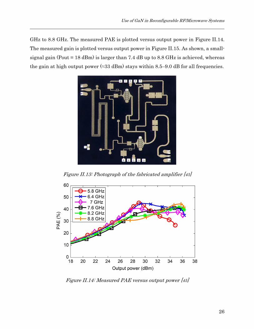
Use of GaN in Reconfigurable RF/Microwave Systems
26
GHz to 8.8 GHz. The measured PAE is plotted versus output power in Figure II.14.
The measured gain is plotted versus output power in Figure II.15. As shown, a small-
signal gain (Pout = 18 dBm) is larger than 7.4 dB up to 8.8 GHz is achieved, whereas
the gain at high output power (≈33 dBm) stays within 8.5–9.0 dB for all frequencies.
Figure II.13: Photograph of the fabricated amplifier [45]
Figure II.14: Measured PAE versus output power [45]

A Review of the Literature of Gallium Nitride Technology
27
Figure II.15: Measured gain versus output power [45]
In [46] using tunable capacitors in the input and output matching
networks, a 2.45 GHz GaN HEMT operating class and frequency reconfigurable
power amplifier is reported. Figure II.16 and Figure II.17 show, respectively, the
concept of impedance matching conditions and a topology of the photograph of the
proposed reconfigurable PA. The proposed PA can be reconfigured to operate in class
A or class B to achieve, respectively, an extreme high linearity and high efficiency
where high linearity is not strictly required. As a result, the proposed reconfigurable
PA design can be reconfigured for multiple bands and for switching between
operating classes. This reconfigurability is clearly seen in Figure II.18, Figure II.19
and Figure II.20 where gain, output power and PAE versus the swept input power,
respectively, are plotted.

Use of GaN in Reconfigurable RF/Microwave Systems
28
Figure II.16: The concept of impedance matching conditions of the band and class
reconfigurable power amplifier [46]
Figure II.17: Photograph of the fabricated class-reconfigurable power amplifier [46]
Figure II.18: Simulated gain verses input power at different matching states [46]

A Review of the Literature of Gallium Nitride Technology
29
Figure II.19: Simulated output power verses input power at different matching
states [46]
Figure II.20: Simulated power added efficiency verses input power at different
matching states [46]
In [47], for the first time a novel technique on how to combine the
advantages of the high power handling capabilities of GaN devices and microfluidic
channels integrated in a multilayer organic substrate by designing a reconfigurable
GaN-based PA at 2.4 GHz and 5.8 GHz is designed. An illustration of the packaged
PA is shown in Figure II.21. The new technique regarding the design of tunable
source and load matching networks frequency response is based on using different

Use of GaN in Reconfigurable RF/Microwave Systems
30
fluids (acetone for 2.4 GHz and air for 5.8 GHz) injected inside their respective
micromachined channels. As reported, the fabricated PA provides an output power of
35 dBm with a PAE of 36.41% at 2.3 GHz for an input power of 21 dBm, while at 5.7
GHz an output power of 36.88 dBm is achieved with a PAE of 44.03% for an input
power of 25 dBm. These measured results are plotted in Figure II.22 and Figure II.23
for, respectively, acetone and air configuration.
Figure II.21: (Left) Top and cross sectional view and (Right) Picture of the packaged
PA [47]
Figure II.22: Acetone configuration: measurements at 2.3 GHz, simulations at 2. 4
GHz [47]

A Review of the Literature of Gallium Nitride Technology
31
Figure II.23: Air configuration: measurements at 5.7 GHz, simulations at 5.8 GHz
[47]
More studies revealed that due to the drawbacks of GaAs MMIC HPA as
low efficiency and limited output power level have made it not to be a competent
candidate of power chips against the high efficiency of GaN MMICs technology [39].
In this same reference, a GaN-based high power amplifier with output power of 85 W
and operating at S-band is reported. In 2014, an investigation [38] revealed that the
next generation of GaN MMICs will cover more functionalities on the same chip.
Multifunctional MMICs will allow very compact Tx/Rx module designs, and will
reduce the number of active devices [38].
In this context, this thesis research is focused to demonstrate the use of
GaN on highly efficient reconfigurable designs for broadband RF/microwave
applications operating below 10 GHz. GaN components such as varactors and
switches used for tunable purpose are firstly fabricated, characterized and then
modeled. The proposed models are used to achieve the reconfigurability of
RF/microwave circuits. Tunable phase shifter, reconfigurable 3-dB 90° hybrid
coupler, tunable frequency oscillator, beam switching antenna array and matching
reconfigurable patch antenna are developed along with the development of GaN
modeling varactors and switches, and are presented as applications results of this
thesis research. A current literature review of these reconfigurable cited circuits will
be presented along with the realization of these designs later in chapter IV.

Summary
32
IV. Summary
In this chapter the properties of GaN technology have been reviewed,
discussed and compared with the commonly used semiconductor technologies. It has
been clearly shown that GaN technology is a great promising semiconductor
candidate for applications that high power and high frequency are required as well
as high temperature. Its disadvantages and difficulties are also studied presented
and discussed. Additionally the features and limitations of the used AlGaN/GaN
process throughout this thesis provided by NRC were summarized and presented.
Furthermore, an overview of the ability to use GaN technology for tunable purposes
such as power amplifier discussed. We also reviewed some previous work done on the
development of reconfigurable power amplifier circuits using GaN technology that
are used in Tx/Rx modules.

GaN Varactor and Switch Devices Modeling
33
Chapter III
---------------------------------------------------------------------------------------------------------------------
GaN Varactor and Switch Devices
Modeling
I. Introduction
A general purpose reconfigurable integrated RF/microwave circuit could be
realized using a promising semiconductor technology for the active device, and an
interconnection technique such as wire-bonding technique to compact all the circuits.
Recent technology trends favor greater integration of electronic devices and radiating
elements, greater functionality and reconfigurability (on a single chip or via multi-
chips), as well as high operating frequency/power with excellent efficiency and
linearity. Such are the needs for next generation of Tx/Rx modules.

Introduction
34
For the proposed thesis research, GaN-based varactor and switch
components will be pursued; the main features of this type of semiconductor
technology being its high power with high efficiency. Compact reconfigurable circuits,
such as tunable phase shifter, reconfigurable 3-dB 90° hybrid coupler, tunable
frequency oscillator, beam switching antenna array and matching reconfigurable
patch antenna based on these developed varactors and switches will be studied. The
first part of the work is devoted to active GaN device development and
characterization. The second part addresses the integration and design aspects of the
reconfigurable proposed circuits.
GaN technology to date has seen very little application to signal control
devices such as varactors and switches. These two elements are key points to realize
phase shifters (both continuous and discrete state), frequency reconfigurable circuits,
and signal path selection circuits for beam switching or Tx/Rx selection.
Our investigation considers modeling in small- and large-signal of both
GaN varactor devices and GaN switch devices, as outlined in the “Work Plan” chart
below (see Figure III.1). The design of these GaN components was realized using the
Canadian National Research Council (NRC) GaN HEMTs monolithic microwave
integrated circuit (MMIC) processes. Three NRC GaN HEMTs processes, such as,
GaN150v0 with a gate length of 0.15 um, GaN500v1 with gate length of 0.5 um and
GaN500v2 which is the developed version of GaN500v1, have been used to
manufacture the varactor and the switch devices.
An accurate large signal model requires extensive laboratory equipment to
extract all the effects related to high power GaN devices, such as thermal and
trapping effects typically present in GaN devices. Carleton University is not as well
equipped with these laboratory facilities as are the NRC or IETR. Due to our
incapability to have large signal measurement facilities, only small signal
measurement will be presented and discussed. However, for varactors fabricated
GaN Varactor and Switch Devices Modeling
35
using GaN500v2, we finally succeed to do large signal measurements. These
measurements have been done at XLIM at University of Limoges, France.
Figure III.1: Work Plan
First step, we start investigating varactor devices. For this, two NRC GaN
HEMTs processes, GaN500 and GaN150, have been used to manufacture the devices.
At this time the current version (v1) of GaN500 process was used; while for GaN150,
the process was still under-development and its initial version (v0) was used which
was non-commercialized one. Many size different devices have been manufactured
and characterized in only small signal measurements, and then a small signal model
has been implemented. This model describes clearly the behavior of GaN based
varactor. Following the development of NRC GaN HEMTs process, another
fabrication run has been launched to manufacture other varactor devices with
different sizes and by using, in this time, only the newly developed version of GaN500
process, version 2. This time, small signal as well as large signal measurements have

GaN-based Varactors Diodes Modeling
36
been done on these novel realized varactors, respectively, to validate the proposed
small signal model developed from GaN500v1 process’ devices and to verify their
capabilities in terms of different power levels. Secondly, single GaN switches with
different sizes have been fabricated and measured in only small signal. A model is
presented and discussed. These varactor and switch models will be used to simulate
and design reconfigurable RF/microwaves designs shown in the chapter IV.
II. GaN-based Varactors Diodes Modeling
1. Review of GaN HEMT for Power Varactors Diodes
Applications
GaN HEMTs semiconductor devices are no longer limited to RF power
amplifier applications, but having been extended to other applications such as LNAs
[48], VCOs [49], mixers [51], and phase shifters [50]-[52]. Furthermore, reconfigurable
RF circuits, with high power/frequency, and excellent linearity, are in great demand.
Varactors are key components in the design of these reconfigurable circuits [53] for
microwave and millimeter wave applications. The varactor diodes can be fabricated
from either p-n or Schottky junctions and both cases are under research today.
The superior characteristics (i.e high-temperature operation due to large
energy band gaps, high breakdown field, high saturation velocities of electrons, etc)
make GaN heterostructures promising candidates for realizing high power/tuning
voltage varactors diodes. Up to now, the progress on developing GaN varactors have
been limited and only a few works have been already reported. Based on GaN HEMT
technology, some varactors have previously been reported, mostly employing a Metal-
Semiconductor-Metal (MSM) junction [53]-[54]-[55]-[56] or Schottky barrier contact
[57]-[58]-[59].
Later 2002, one of the first investigated GaN varactor work was reported
in [53]. This work investigates the properties of MSM diodes that are based on an

GaN Varactor and Switch Devices Modeling
37
AlCaN/GaN HEMT layer structure (MSM-2DEG), which shown that devices made in
this material system are realizable with tuning capacitance range. As can be seen
from Figure III.2, the capacitance is constant between 2.7 and -2.7V and within a
very small voltage range of about 0.3 V the capacitance starts getting changed. The
reported measured CMAX/CMIN ratios vary from 5 to 100 and were dependent on
electrode geometry. This investigation shown clearly that these ratio values were
exceeding those ratios for varactor diodes in GaAs. However, a high series resistance
varies from 40 Ω to 70 Ω was extracted and these values were dependent on the
electrode spacing from 0.5 um to 2 um. This high series resistance of the device, which
was announced as a challenge for varactors diodes, can affect directly the figure of
merit, quality factor (Q-factor), of the device. In addition, this high value of series
resistors is due to the unavoidable ohmic contact resistance. Researchers have begun
to investigate the possibilities in order to reduce this specific contact resistance.
Figure III.2: C-V characteristics of devices with different electrode length (spacing =
1 um, width = 50 um) [53]
In [54], a work focused on characterizing the Q-factor of MSM AlGaN/GaN
varactors that operate in RF range was reported. The ohmic contact is eliminated and
replaced by a Schottky contact, resulting in reduced overall series resistance and
higher peak Q-factor. A standard AlGaN/GaN HEMT process was fully compatible
for manufacturing this MSM varactors. The C-V measurements (see Figure III.3)

GaN-based Varactors Diodes Modeling
38
revealed that the device was capable to valid the rapid change on capacitances values
over a small range of bias voltage. At 1.1 GHz, the capacitance tuning range was
varying from 1.62 to 0.12 pF corresponding to a CMAX/CMIN ratio of 13.5. Moreover, a
high series resistors values were still achieved. The dependence of the Q-factors on
the bias voltage at 1.1 GHz is illustrated in Figure III.4. From both Figure III.3 and
Figure III.4, it can be seen that the value of Q-factor decreased as well as the series
resistor value increases. A physical equivalent circuit model was reported to explain
the behavior of the voltage controlled capacitance and the corresponding Q-factor. It
was revealed that the fundamental limit on the Q-factor in the intermediate
capacitance range is the rapidly increasing channel resistance when the channel is
depleted. Although, it was reported that further improvement of the Q-factor has to
come from modification of the conventional single-channel HEMT using double- or
multiple-channel structure in which additional low impedance current paths are
available.
Figure III.3: Extracted capacitance (black line) and resistance (white line) of the
MSM varactor over the entire bias range at 1.1 GHz. The inserted schematic shows
the first-order equivalent circuit of the MSM varactor [54]

GaN Varactor and Switch Devices Modeling
39
Figure III.4: Q-factor versus tuning bias at 1.1 GHz [54]
Another investigation MSM GaN varactor was reported in 2012 in [55]. In
this work, a MSM varactor diodes on top of an AlGaN/GaN-based epitaxial structure
is proposed to the fast surge protection application. This works was focused on
developing a surge to protect electronic devices against the natural or manmade surge
threats, including lightning, electromagnetic pulse (EMP), electrostatic discharge
(ESD) etc. Figure III.5 shows the schematic diagram of an AlGaN/GaN-based
varactor used in this study while the C-V curves of the surface untreated and the
sulfur-treated AlGaN/GaN-based MSM-2DEG varactors used in this study are
presented in Figure III.6. This investigation showed that the varactor exhibits great
potential to improve the surge protection for GaN-based HEMTs. Therefore, the
fabricated process significantly affects the capacitance swing of MSM-2DEG
varactors. Due to the variable impedance characteristics of the varactor, it is either
within the high impedance region for blocking the surge energy or within the low
impedance region for passing normally the signal.

GaN-based Varactors Diodes Modeling
40
Figure III.5: A Schematic diagram of the AlGaN/GaN-based varactor [55]
Figure III.6: Measured C-V curves of the untreated and sulfur-treated AlGaN/GaN-
based MSM-2DEG varactors [55]
In 2015, by the same group researchers of [55], a MSM varactor study has
been reported in [56]. Here, the performance of the AlGaN/GaN MSM-2DEG varactor
with different dielectric films deposited by the E-beam deposition is investigated. In
addition, different dielectric films are studied to verify the effect of the dielectric
material on the capacitance ratio and the bias voltage of varactors. For this, three
dielectric films have been used, such as, SiO2, Gd2O3, and Si3N4 to conduct this
study. Figure III.7 illustrates the schematic diagram of the AlGaN/GaN MSM-2DEG
varactor used for this study. From Figure III.8, it was observed that the capacitance

GaN Varactor and Switch Devices Modeling
41
tuning ranges are almost identical irrespective of whether with dielectric film or not.
However, the capacitance ratio (CMAX/CMIN) for each varactor is affected by the type
of the dielectric film used. It was proved that the varactors with the SiO2 and Gd2O3
dielectric films offer the benefit of a lower leakage current. It was also observed that
the CMAX, the CMIN and the capacitance ratios show the same tendency of decreasing
for varactors with dielectric films and are proportional to the increasing of the
electrode areas.
Figure III.7: Schematic diagram of the AlGaN/GaN MSM-2DEG varactor of the
samples prepared in this study [56]

GaN-based Varactors Diodes Modeling
42
Figure III.8: Capacitance-Voltage (C-V) characteristics of varactors with different
electrode areas (a) without any dielectric film, (b) with SiO2 film, (c) with Gd2O3
film, and (d) with Si3N4 film. Measurement frequency = 1MHz, electrode area =
37922, 85224, 151122, and 236472 μm2, respectively [56]
In [57], a novel GaN-based high frequency varactor diode was reported.
This main goal of this work is to investigate the high frequency performances
expected from such GaN-based Schottky barrier varactor diode. The structure used
in this work consists of a 2 μm bottom ohmic (n+) contact layer and a 300 nm lightly
doped (n-) GaN layer which is grown on top of the ohmic layer. The ohmic contacts
(Ti/Al/Ti/Au) were deposited once the mesa mask was isolated by Ar etching and then
Pt was deposited which forms the Schottky contact metal. The schematic of the GaN
Schottky varactor structure is shown in Figure III.9. It was shown that epilayer
designs can help in controlling such characteristics. As shown in Figure III.10, the

GaN Varactor and Switch Devices Modeling
43
maximum capacitance at 0 V bias is 40.476 fF and the minimum capacitance is about
26.4fF when a bias of less than -7 V is applied. This reported varactor had a
breakdown voltage of 20 V and a cut-off frequency of 360 GHz.
Figure III.9: Schematic Cross-sectional view of the GaN Schottky Varactor [57]
Figure III.10: C-V characteristics of the GaN Schottky Varactor [57]
Based on Schottky barrier, another work was reported in [58]. In this work,
a design of InGaN/GaN schottky diodes with enhanced voltage handling capability
with vertical geometry was discussed. It is, therefore, illustrated that a higher voltage
handling capability may be obtained with a suitable InGaN surface layer design.
Figure III.11 schematically shows the structure of a GaN varactor. Furthermore, the
depletion width W varies in the n- region under several external bias voltage, this
resulting to a change in equivalent C as well as in its associated series resistors R.
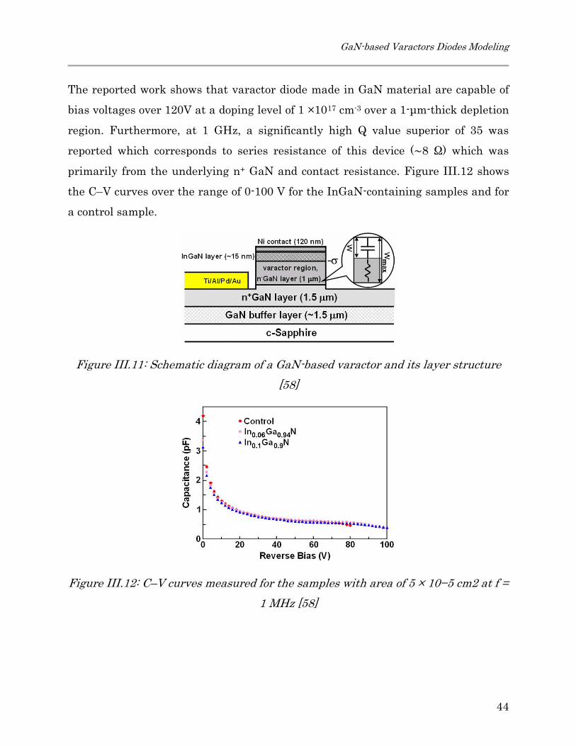
GaN-based Varactors Diodes Modeling
44
The reported work shows that varactor diode made in GaN material are capable of
bias voltages over 120V at a doping level of 1 ×1017 cm-3 over a 1-μm-thick depletion
region. Furthermore, at 1 GHz, a significantly high Q value superior of 35 was
reported which corresponds to series resistance of this device (∼8 Ω) which was
primarily from the underlying n+ GaN and contact resistance. Figure III.12 shows
the C–V curves over the range of 0-100 V for the InGaN-containing samples and for
a control sample.
Figure III.11: Schematic diagram of a GaN-based varactor and its layer structure
[58]
Figure III.12: C–V curves measured for the samples with area of 5 × 10⁻⁵ cm2 at f =
1 MHz [58]

GaN Varactor and Switch Devices Modeling
45
Two years later, on 2012, the same group researchers of [58] reports a new
work [59] where the critical design considerations for achieving GaN-based high
voltage, high Q factor and high linearity microwave varactors were summarized and
were discussed. In addition, detailed performances for a real fabricated GaN-based
anti-parallel varactor diode structure that simultaneously achieving high Q, high-
breakdown voltage and high linearity were presented. This investigation was based
on using the same GaN structure presented in Figure III.11. It was highlighted that
heavily doped semiconductor material is required to minimize the series resistor and
achieve a high Q-factor. However, in order to achieve high breakdown voltage, the
semiconductor needs to be lightly doped to keep the electric field in the semiconductor
below its critical electric field. Furthermore, the two anti-parallel diodes structure
was used to investigate the varactor linearity. It was reported that by using this
structure, the RF signal induced capacitance variation is minimized. The linearity of
the varactor diode is thus significantly improved. Figure III.13 shows the simulated
C-V curves for single and two anti-parallel structures, while in Figure III.14, Q-factor
versus the reverse external bias is depicted.
Figure III.13: Capacitance-voltage curves for (a) single diode structure and (b) two
anti-parallel diode structure [59]

GaN-based Varactors Diodes Modeling
46
Figure III.14: Q factor versus reverse external bias for an anti-parallel varactor at f
= 1 GHz, 2 GHz and 3 GHz. Each diode has an area of 3.8×10⁻⁵ cm2 [59]
2. Realized GaN HEMT-based Varactor Diodes
These previous reported works present good performance in term of high
breakdown voltage, high Q-factor, and high linearity; however, the limited
capacitance tuning range is still a challenge. Furthermore, to achieve good
performance, most of these reported works require some changes in epitaxial and
mask layer of the GaN HEMT process which results in a complexity of fabrication
and cost increasing. These challenges have limited the progress of developing
varactor diodes. In order to overcome the two above-mentioned drawbacks, here, for
this thesis work, the varactor diode is realized by connecting together the drain and
source terminations thus resulting in a single Schottky junction which can be
considered as planar schottky varactor diode (PSVD) [68].
The bias potential VG is then applied across the drain/source and gate
terminations. This kind of varactor diodes do not require any additional selective
changing in the epitaxial layers of the HEMT process. As a result, a standard GaN
HEMT process can be used which minimize their cost production compared to the
other reported type of varactor diodes. However, GaN-based PSVDs have not been
widely used because of the unavailability of accurate large and small signal models
which become our motivations to develop them. We investigate the equivalent

GaN Varactor and Switch Devices Modeling
47
capacitance CEq and the equivalent series resistance REq of the varactor, when the
overall impedance is considered as a simple series RC circuit.
3. GaN500v1 and GaN150v0 Varactor Devices
Figure III.15 illustrates the layout design for one varactor device. To
compare between the two processes (GaN500v1 and GaN150v0), two samples of each
process with different fingers width are studied as detailed in Table III.1:
Table III.1: Presented GaN500v1 and GaN150v0 Devices Information
Device Terminology
Number of Fingers
Fingers Width
Fingers Length
Process Terminology
W40L0.5 2 40 μm 0.50 μm GaN500v1
W100L0.5 2 100 μm 0.50 μm GaN500v1
W50L0.15 2 50 μm 0.15 μm GaN150
W100L0.15 2 100 μm 0.15 μm GaN150
Figure III.15: Schematic cross-section of HEMT, showing contacts and epitaxial
structures, and physical equivalent circuit origin at pinch-off (VG = -3.5 V)
The W40L500v1 device is shown in Figure III.16 when it is positioned in
Microwave probe test.

GaN-based Varactors Diodes Modeling
48
Figure III.16: W40L500v1 Device in Microwave Probe Test
3.1 Small Signal Modeling
The physical origins of the varactor device’s equivalent model of both NRC
GaN process are shown in the cross-sectional view in Figure III.15. Rg, Lg, Rd, Ld, Rs
and Ls are, respectively, the metal resistance and the parasitic inductance of the gate,
of the drain and of the source. Rcst is the constant resistor and is determined by the
AlGaN layer thickness. For GaN500v1 process, the thickness is about 20nm and Rcst
is 1Ω.mm. Rsheet refers to the channel resistance which is also constant and is
determined by the two dimensional electron gas (2DEG), it is 300Ω/, while Rdep
represents the resistance under the depletion region which is affected by the bias
voltage, VG, and changes slightly when the channel starts to deplete, this leads to a
change in the series resistor of the equivalent circuit. Cdep represents the depletion
capacitance; it changes significantly with VG. The physical equivalent circuit shown
in Figure III.15 could be transformed to a simple equivalent RC circuit model as
shown in Figure III.17.
Figure III.17: Varactor equivalent circuit model

GaN Varactor and Switch Devices Modeling
49
Lpara, REq, CEq and RLeak, respectively, are the parasitic inductor, the
equivalent series resistor, the equivalent series capacitance and the leakage resistor
when the diode presents forward conduction current flow. The effect of Lpara is
negligible at low frequencies while the value of RLeak is very high (about 8 GΩ). The
on-wafer RF measurements were performed with an Agilent VNA Network Analyzer
over a frequency range of 0.1-20 GHz with a RF power of -15 dBm. As can be seen in
Figure III.18, Figure III.19, Figure III.20 and Figure III.21, a good match between
the experimental results and the simulation model results is generally achieved. For
GaN150v0, agreement is nearly perfect, while for GaN500v1 there are some issues
with the larger device at high frequencies for -6 V bias. Here the channel is fully
depleted and some parasitic inductances are not captured in the equivalent model.
For VG of -3 V, -4 V and -6 V, the parameter values of the equivalent model are
presented in Table III.2.
Table III.2: Parameters values of the equivalent circuit
Device VG (V) Lpara (pH) REq (Ω) CEq (fF)
W40L0.5 -3 25 17 205
-4 25 50 190.7
-6 25 15.5 82.7
W100L0.5 -3 30 6.9 533
-4 30 13.3 439
-6 30 6.16 220
W50L0.15 -3 10 5 148
-4 10 9.7 98
-6 10 4.77 40
W100L0.15 -3 20 4.9 286
-4 20 8.3 189
-6 20 5 81

GaN-based Varactors Diodes Modeling
50
Figure III.18: Measured (lines) and Simulated (Dot) S11-parameter for G W40L0.5
Figure III.19: Measured (lines) and Simulated (Dot) S11-parameter for W100L0.5

GaN Varactor and Switch Devices Modeling
51
Figure III.20: Measured (lines) and Simulated (Dot) S11-parameter for W50L0.15
Figure III.21: Measured (lines) and Simulated (Dot) S11-parameter for W100L0.15
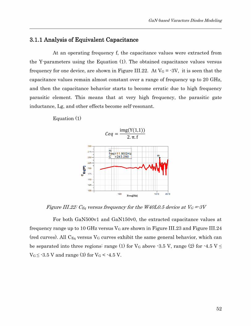
GaN-based Varactors Diodes Modeling
52
3.1.1 Analysis of Equivalent Capacitance
At an operating frequency f, the capacitance values were extracted from
the Y-parameters using the Equation (1). The obtained capacitance values versus
frequency for one device, are shown in Figure III.22. At VG = -3V, it is seen that the
capacitance values remain almost constant over a range of frequency up to 20 GHz,
and then the capacitance behavior starts to become erratic due to high frequency
parasitic element. This means that at very high frequency, the parasitic gate
inductance, Lg, and other effects become self-resonant.
Equation (1)
𝐶𝑒𝑞 =img(Y(1,1))
2. π. f
Figure III.22: CEq versus frequency for the W40L0.5 device at VG =-3V
For both GaN500v1 and GaN150v0, the extracted capacitance values at
frequency range up to 10 GHz versus VG are shown in Figure III.23 and Figure III.24
(red curves). All CEq versus VG curves exhibit the same general behavior, which can
be separated into three regions: range (1) for VG above -3.5 V, range (2) for -4.5 V ≤
VG ≤ -3.5 V and range (3) for VG < -4.5 V.

GaN Varactor and Switch Devices Modeling
53
Figure III.23: Extracted and Simulated CEq versus VG for GaN500v1 Devices
Figure III.24: Extracted and Simulated CEq versus VG for GaN150 Devices
For range (1) and range (3) corresponding to the device’s CMAX and CMIN,
respectively, the capacitance values do not change. However, in range (2), the
capacitance values change significantly, and rapidly over a small DC bias range from
-4.5 V to -3.5 V. Based on these observations, we conclude that the capacitance tuning
range is limited, and the region of variable capacitance exists only over a small
reverse voltage of 1V. The capacitance CEq is given by the following equation:
Equation (2)
𝐶𝑒𝑞 =Ԑ𝑟. 𝐴
d 𝑤𝑖𝑡ℎ 𝐴 = 𝑁.𝑊. 𝐿
Where, Ԑr is the permittivity of the material, A is the finger area, d is the
distance between surface and 2DEG channel (or the depth of the depletion region), N
is the number of fingers, W and L are the width and the length of finger. From
Equation (2), the capacitance value depends on d. In other words, when d varies, this

GaN-based Varactors Diodes Modeling
54
leads to a change in the capacitance value. The maximum and the minimum CEq are
obtained when the d reaches its minimum (dmin) and maximum (dmax), respectively.
Furthermore, the capacitance value depends on the finger area. The variation in d is
controlled by VG and leading to the change in CEq which could be summarized as
follow:
Range (1): Before the channel starts depleting; CEq is at its maximum value
where the depletion region is at dmin.
Range (2): The channel starts depleting until it is completely depleted. The
depleted region in the channel shrinks quickly, resulting in a rapid increase of
CEq.
Range (3): The channel is completely depleted; CEq is at its minimum values
where the depletion region is at dmax.
In order to describe the nonlinear behavior of CEq for both GaN500v1 and
GaN150v0, analytical equations based on empirical coefficients are derived from the
measurements. The exponential of tangent hyperbolic function yields an approximate
analytical expression for CEq versus VG. It is seen that Equation (3) accurately
describes the dependency of junction capacitance upon applied reverse bias, VG, for
all characterized devices.
Equation (3)
𝐶𝑒𝑞 = 60𝐴
𝑀(1 +
1
𝑀)(𝑒𝑡𝑎𝑛ℎ[2.5𝑉𝑔+11]) + 𝑘)
The parameters M and K can be adjusted to properly fit the CEq equation
to the measured characteristics of an arbitrary varactor size. According to Matlab
simulations, the values of M and K can be fixed, respectively, as 40 and 1.2 for
GaN500v1 devices and as 20 and 0.45 for GaN150 devices. The modeled curves are
plotted in Figure III.23 and Figure III.24 (blue lines). All of these equations are
dependent only on finger geometry (number, width and length of fingers) and on VG.
Equation (3) illustrates the behavior of CEq for GaN500v1 and GaN150v0 devices.
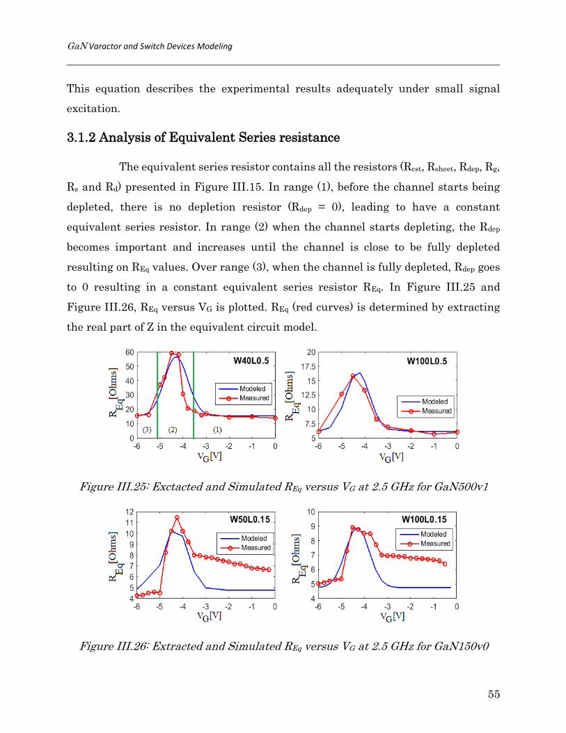
GaN Varactor and Switch Devices Modeling
55
This equation describes the experimental results adequately under small signal
excitation.
3.1.2 Analysis of Equivalent Series resistance
The equivalent series resistor contains all the resistors (Rcst, Rsheet, Rdep, Rg,
Rs and Rd) presented in Figure III.15. In range (1), before the channel starts being
depleted, there is no depletion resistor (Rdep = 0), leading to have a constant
equivalent series resistor. In range (2) when the channel starts depleting, the Rdep
becomes important and increases until the channel is close to be fully depleted
resulting on REq values. Over range (3), when the channel is fully depleted, Rdep goes
to 0 resulting in a constant equivalent series resistor REq. In Figure III.25 and
Figure III.26, REq versus VG is plotted. REq (red curves) is determined by extracting
the real part of Z in the equivalent circuit model.
Figure III.25: Exctacted and Simulated REq versus VG at 2.5 GHz for GaN500v1
Figure III.26: Extracted and Simulated REq versus VG at 2.5 GHz for GaN150v0
GaN-based Varactors Diodes Modeling
56
The nonlinear behavior of REq for both GaN500v1 and GaN150v0 can be
described by analytical equations based on empirical. The REq-VG characteristics is a
Gaussian form, as deduced from Figure III.25 and Figure III.26 (red dotted lines).
Thus the REq-VG characteristics are taken to be:
Equation (4)
𝑅𝑒𝑞𝐺𝑎𝑁500 =44
A[
(
1
√𝑊𝜋Y 8. 10−5)
(𝑒−2(𝑉𝑔+4.35)2) + 𝑌]
Equation (5)
𝑅𝑒𝑞𝐺𝑎𝑁150 = [
(
1
6√𝐴𝜋Y8. 10−5)
(𝑒−2(𝑉𝑔+4.35)2) + 𝑌]
Where A is the finger area. The parameter Y can be adjusted to properly
fit the REq equation to the measured characteristics of an arbitrary varactor size.
According to Matlab simulations, the value Y can be fixed to 14 for GaN500v1 devices
and as 4.75 for GaN150 devices. All of these equations are dependent only on finger
geometry (number, width and length of fingers) and on VG. Equation (4) describes REq
for GaN500v1 devices, while Equation (5) describes REq for GaN150v0 devices. These
equations describe the experimental results adequately under small signal excitation.
Due to these resistance values, a part of the RF available power is consumed by the
devices and losses will occur in the RF signal. More REq is high more losses are high.
A good agreement is obtained, except for REq in range (1) of the GaN150v0 devices. A
slightly more complicated model would be required here to capture the higher
measured REq.
3.1.3 Analysis of Q-Factor
In Figure III.27 and Figure III.28, the Q factor is plotted versus frequency.
Referring to the equivalent model presented in Figure III.17, the Q factor can be
evaluated by the following equation.
Equation (6)

GaN Varactor and Switch Devices Modeling
57
𝑄 =𝑖𝑚𝑔(𝑍(1,1))
𝑟𝑒𝑎𝑙(𝑍(1,1))=
1
(2. 𝜋. 𝑓. 𝐶𝑒𝑞. 𝑅𝑒𝑞)
Figure III.27: Extracted Q factor versus Frequency at VG = -3.5 V for GaN500v1
Figure III.28: Extracted Q factor versus Frequency at VG = -3.5 V for GaN150v0
The Q factor decreases with frequency. It is notable that a minimum Q of
~25 and ~50 was achieved over a range of frequency below 2 GHz, respectively, for
GaN500v1 and GaN150v0. Another most common used figure of merit for varactor is
the cut-off frequency. The cut-off frequency is defined as the frequency at which the
capacitive reactance is equal to the series resistance. Note that the cut-off frequency
is also a function of voltage and that it achieves its maximum value at VB. This FOM
indicates that the maximum operating frequency of the circuit is dependent on the
series resistance and the equivalent capacitance. FOM should be as high as possible,
which can be mathematically given as:
Equation (7)
𝐹𝑐𝑢𝑡_𝑜𝑓𝑓 =1
(2. 𝜋. 𝐶𝑒𝑞. 𝑅𝑒𝑞)
GaN-based Varactors Diodes Modeling
58
At f = 2.5 GHz, maximum values of 164.9 GHz and of 419.2 GHz were
achieved, respectively, for W40L0.5 and W100L0.5 at VG = -5 V. While for W50L0.15
and W100L0.15, the maximum obtained values are 770.6 GHz and 335.9 GHz,
respectively. These obtained values serve as figure of merit to compare with other
varactor diode in terms of frequency operation capability. A comparison between the
two GaN processes in terms of capacitor CEq is presented in Table III.3.
Table III.3: Comparison of capacitance performances between GaN500 and GaN150
GaN500v1 GaN150v0
Capacitance 2.7fF/um 1.5fF/um
CMAX/CMIN 2.4 3.7
Tuning Voltage -4.5 V to -3.5 V -4.5 V to -3.5 V
4. GaN500v2 Varactor Devices
To conduct this second varactors modeling study, many samples with
different sizes have been fabricated with the GaN500v2 process but only three of
them are presented here (see Table III.4). The presented devices are W50L0.5,
W100L0.5 and W200L0.5 (different fingers width).
Table III.4 : Presented GaN500v2 Devices Information
Device Terminology
Number of Fingers
Fingers Width
Fingers Length
Process Terminology
W50L0.5 2 50 μm 0.50 μm GaN500v2
W100L0.5 2 100 μm 0.50 μm GaN500v2
W200L0.5 2 200 μm 0.50 μm GaN500v2
4.1 Small Signal Measurement
The on-wafer RF measurements were performed with an Agilent VNA
Network Analyzer over a frequency range of 0.1-20 GHz with a fixed RF power of -
15dBm, while the control voltage at the gate of varactors, VG, was swept from 0 V to
-10 V with a step of -0.1 V. Because it was observed that from 0 V to -3 V, the
measured results are similar and also from -5 V to -10 V measured results are similar.
So only measurements from -2 V to -6 V will be treated and analysed here. As can be

GaN Varactor and Switch Devices Modeling
59
seen in Figure III.29, Figure III.30 and Figure III.31, a good match between the
experimental results and the simulation model results is generally achieved. For
W100L0.5 and W200L0.5, agreement is nearly perfect, while for W50L0.5 there are
some issues with this device at high frequencies. Here some parasitic inductances are
not captured in the simple proposed equivalent model. As detailed previously, there
are three main ranges that describe the change in the parameters of the varactor
model. Range (1) and range (3) corresponding to the device’s CMAX and CMIN,
respectively, while, range (2) corresponding to the tuning capacitance range. Table
III.5 summarizes the parameter values of the equivalent model at three bias voltage,
such as, VG of -3 V (in range 1), -4 V (in range 2) and -6 V (in range 3).
Table III.5: Parameters values of the equivalent circuit
Device VG (V) Lpara (pH) REq (Ω) CEq (fF)
W50L0.5 -3 5 7.9 466
-4 5 11 375
-6 5 9.5 279
W100L0.5 -3 16 5.3 870
-4 16 7.35 637
-6 16 6.5 501
W200L0.5 -3 100 4.7 1810
-4 100 5.85 1403
-6 100 5.2 1016

GaN-based Varactors Diodes Modeling
60
Figure III.29: Measured (lines) and Simulated (Dot) S11-parameter for W50L0.5
Figure III.30: Measured (lines) and Simulated (Dot) S11-parameter for G W100L0.5

GaN Varactor and Switch Devices Modeling
61
Figure III.31: Measured (lines) and Simulated (Dot) S11-parameter for G W200L0.5
4.1.1 Analysis of Equivalent Capacitance
The same analysis drawn before for GaN500v1 devices will be also used
here to discuss and develop the extracted equivalent capacitance values for
GaN500v2 devices.
As previously mentioned, the capacitance values were extracted from the
Y-parameters using Equation (1). The obtained capacitance values versus frequency
for one device (W50L0.5), are shown in Figure III.32. At VG = -3 V, it is seen that the
capacitance values remain almost constant over a range of frequency up to 8 GHz,
and then the capacitance starts to decrease due to high frequency parasitic elements.
This means that at very high frequency, the parasitic gate inductance, Lg, and other
effects become self-resonant.
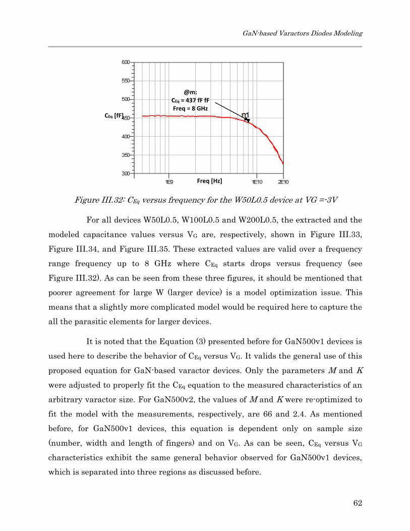
GaN-based Varactors Diodes Modeling
62
Figure III.32: CEq versus frequency for the W50L0.5 device at VG =-3V
For all devices W50L0.5, W100L0.5 and W200L0.5, the extracted and the
modeled capacitance values versus VG are, respectively, shown in Figure III.33,
Figure III.34, and Figure III.35. These extracted values are valid over a frequency
range frequency up to 8 GHz where CEq starts drops versus frequency (see
Figure III.32). As can be seen from these three figures, it should be mentioned that
poorer agreement for large W (larger device) is a model optimization issue. This
means that a slightly more complicated model would be required here to capture the
all the parasitic elements for larger devices.
It is noted that the Equation (3) presented before for GaN500v1 devices is
used here to describe the behavior of CEq versus VG. It valids the general use of this
proposed equation for GaN-based varactor devices. Only the parameters M and K
were adjusted to properly fit the CEq equation to the measured characteristics of an
arbitrary varactor size. For GaN500v2, the values of M and K were re-optimized to
fit the model with the measurements, respectively, are 66 and 2.4. As mentioned
before, for GaN500v1 devices, this equation is dependent only on sample size
(number, width and length of fingers) and on VG. As can be seen, CEq versus VG
characteristics exhibit the same general behavior observed for GaN500v1 devices,
which is separated into three regions as discussed before.
CEq [fF]
Freq [Hz]
@m: CEq = 437 fF fF Freq = 8 GHz

GaN Varactor and Switch Devices Modeling
63
The maximum value of capacitance (before the channel starts depleting) is
observed for -3.4 V ≤ VG ≤ 0 V (range 1) and values of 466 fF, 870 fF and 1810 fF were
extracted, respectively, for W50L0.5, W100L0.5 and W200L0.5 designs. While the
minimum value (the channel is completely depleted) is observed for -10 V ≤ VG ≤ -4.5
V (range 3) and values of 278 fF, 501 fF and 1016 fF were extracted for, respectively,
W50L0.5, W100L0.5 and W200L0.5 designs. As a result, CMAX/CMIN ratio about 1.7 is
achieved for all devices. In addition, it was observed that CMAX and CMIN values
remain almost constant over a range of frequency up to almost 8 GHz and then starts
to drop significantly due to high frequency parasitics. The -3.4 V represents the
pinched of voltage of this device where the channel starts depleting. As highlighted
before for GaN500v1 devices, in range (2), the capacitance values change significantly
and rapidly over a small DC bias range of 1 V. This behavior is also observed for the
devices using the GaN500v2.
Because we are essentially focused on the range (2) where capacitance
values change significantly, the x-axis of all C-V plots is delimited from -2 V to -6 V.
Values from 0 V to -2 corresponding to CMAX are stable as well as ones from -6 V to -
10 V corresponding to CMIN.
Figure III.33: Extracted and Simulated CEq versus VG for W50L0.5
-6 -5.5 -5 -4.5 -4 -3.5 -3 -2.5 -2250
275
300
325
350
375
400
425
450
475
500
525
550
Modeled
Measured
VG [V]
CEq [fF]
range 3 range 2 range 1
W50L0.5

GaN-based Varactors Diodes Modeling
64
Figure III.34: Extracted and Simulated CEq versus VG for W100L0.5
Figure III.35: Extracted and Simulated CEq versus VG for W200L0.5
By comparing equivalent capacitance values extracted from GaN500v1
samples and from GaN500v2 samples, it was revealed that the achieved capacitance
values from a device size manufactured with GaN500v2 are at least twice larger than
those achieved with the same device size fabricated with GaN500v1 process.
However, the overall calculated CMAX/CMIN ratios for GaN500v2 devices are smaller
(~1.7) than ones calculated from GaN500V1 devices (~2.4). This significant change in
equivalent capacitance values is essentially due to the additional field plate layer
added in GaN500v2. As discussed in the GaN500 design manual provided by NRC, it
should be pointed out that all devices included in GaN500v1, do not employ field plate
-6 -5.5 -5 -4.5 -4 -3.5 -3 -2.5 -2450
500
550
600
650
700
750
800
850
900
950
Modeled
Measured
-6 -5.5 -5 -4.5 -4 -3.5 -3 -2.5 -2800
900
1000
1100
1200
1300
1400
1500
1600
1700
1800
1900
2000
Modeled
Measured
VG [V]
CEq [fF]
VG [V]
CEq [fF]
W200L0.5
W100L0.5

GaN Varactor and Switch Devices Modeling
65
designs. However, the shape of the gates, using GaN500v1, results in better
frequency performance, but slightly lower breakdown voltage compared to
GaN500v2. For GaN500v1, values of 27 GHz and 75 GHz were reported by NRC,
respectively, for fT and for fmax. The process is suitable for 20V maximum drain voltage
bias. While for GaN500v2 process, a field plated design is included in this version,
and devices exhibit much lower gate leakage than in GaN500v1. However, RF
performance frequency decreased; a fT of 12 GHz and fmax of 24 values were measured
and reported for this version. The process version is suitable for 40V maximum drain
voltage, and yields power levels of ~5 W/mm. We assume that this additional field
plate layer is the main parameter behind the significant increase in the equivalent
capacitance values.
4.1.2 Analysis of Equivalent Series Resistance
The equivalent series resistor extracted from measurement versus bias
voltage is depicted in Figure III.36 for all studied devices. This series resistor is not
impacted by the frequency, so these extracted values are valid at all frequencies.
Here the same general behaviour observed before for GaN500v1 is also noticed for
the devices fabricated with GaN500v2, expect that the values of the series resistor
are significantly different from a process version to another one.
Unlike the GaN500v1 devices where an analytic expression was introduced
to describe the behavior of REq versus VG, here for GaN500v2 devices, as can be clearly
seen the equivalent series resistor values do not change significantly and this is
observed for all devices, so a mean value can be adopted as a fixed value to describe
the REq for a specific device size. In addition, it was observed than more the device
size increases more the REq decreases. The maximum peak value of REq is observed
on range (2) when the channel starts depleting because the depletion resistor (Rdep)
becomes slightly important and increases until the channel is close to be fully
depleted. This behavior has been also observed for GaN500v1 process’ devices. It
should be pointed out the overall series resistor values extracted from GaN500v2

GaN-based Varactors Diodes Modeling
66
devices are smaller than ones found with the previous process version (GaN500v1).
In our point of view, this significant drop in series resistor can be due to the
development occurred out on the stack of epitaxial layers and masks of the process to
reduce the dynamic on-resistance and the Ohmic contact resistance that are
constituting the series equivalent resistor (REq).
As mentioned in chapter II, the trapping electrons phenomena in
AlGaN/GaN HEMTs structure is directly reducing the sheet electron density in the
channel, leading to increase dynamic Ron and provoking drain current dispersion.
Moreover, many efforts for high performance AlGaN/GaN HEMTs have been made
to suppress this current dispersion issue and increased Ron, which are directly
related to modification of surface/interface states in AlGaN/GaN heterostructures.
These modifications are surface passivation [60], a thin AlN barrier layer in
AlGaN/GaN interface [61], application of a field plate [62], surface treatments with
chemicals or plasma [63], and postgate-annealing [64]. On the other hand, in spite of
the rapid development and the studies of GaN-based HFETs, achieving a low Ohmic
contact resistance value still one important issue concerning these devices [65]-[66]
and has a great effect on the output signal during device operation. Low Ohmic
contact resistance is crucial to realization of good RF and power performances of
AlGaN/GaN HEMTs heterojunction devices. As a matter of fact, in terms of power
consumption, high Ohmic contact resistance values cause high electrical power losses
and increase self-heating problem. For example, if the contact resistor is decreased
from 10-5 to 10-6 Ωcm2, a reduction of 60% of the power consumption could be achieved
for devices with breakdown voltage of 600 V [67].
Due to the restricted information, we could not have information on how
NRC group researchers have improved GaN500v2 process to reduce the Ohmic
contact resistance or/and Ron. However, it is reported, by NRC in design manual of
GaN500v2 [31], that a field plate is applied to all devices fabricated with GaN500v2.
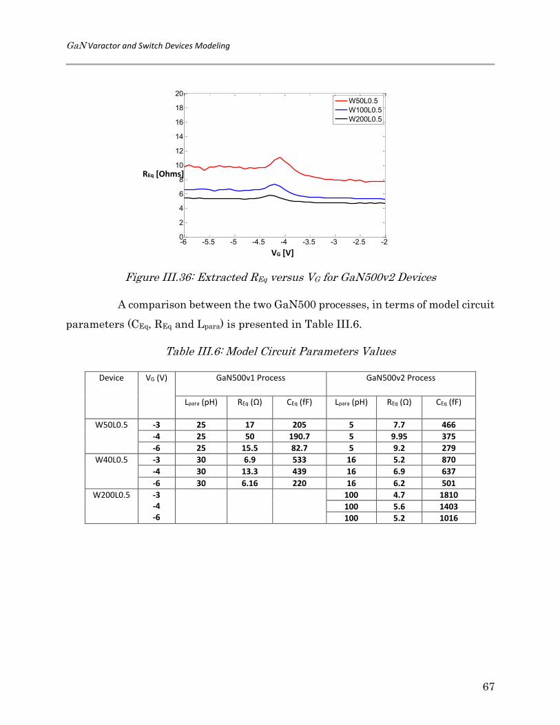
GaN Varactor and Switch Devices Modeling
67
Figure III.36: Extracted REq versus VG for GaN500v2 Devices
A comparison between the two GaN500 processes, in terms of model circuit
parameters (CEq, REq and Lpara) is presented in Table III.6.
Table III.6: Model Circuit Parameters Values
Device VG (V) GaN500v1 Process GaN500v2 Process
Lpara (pH) REq (Ω) CEq (fF)
Lpara (pH) REq (Ω) CEq (fF)
W50L0.5 -3 25 17 205 5 7.7 466
-4 25 50 190.7 5 9.95 375
-6 25 15.5 82.7 5 9.2 279
W40L0.5 -3 30 6.9 533 16 5.2 870
-4 30 13.3 439 16 6.9 637
-6 30 6.16 220 16 6.2 501
W200L0.5 -3 -4 -6
100 4.7 1810
100 5.6 1403
100 5.2 1016
-6 -5.5 -5 -4.5 -4 -3.5 -3 -2.5 -20
2
4
6
8
10
12
14
16
18
20
W50L0.5
W100L0.5
W200L0.5
VG [V]
REq [Ohms]

GaN-based Varactors Diodes Modeling
68
4.2 Large Signal Measurements
As we have just presented, the small signal analysis leading to propose a
circuit model has been discussed. In addition, analytical expressions describing the
general behavior of CEQ and REq for several DC bias were introduced. Following our
original modeling and analysis of GaN-based varactor diodes, by using only a
standard GaN HEMTs process; here, the effect of larger power signal is studied and
presented to complete the analysis of GaN varactor small and large signal modeling.
Unlike to GaN500v1 devices, the newly developed version of GaN500v2 is used for
manufacturing the samples which have been measured in large signal
measurements.
Here the measurement calibration has been done at a fundamental
frequency of 5 GHz. The measurement method consists in performing periodic CW
time-domain large-signal load-pull RF measurements using Large-Signal Network
Analyzer (LSNA). The LSNA can measure the harmonics of the high voltages and
high currents at the DUT planes from 1GHz up to 18 GHz with a dedicated test bench.
Thanks to on-wafer absolute and relative calibrations with absolute phase reference
of LSNA, the time-domain RF voltages and currents (at fundamental and harmonic
frequency [f0, 2f0 and 3f0]) and periodic CW power performance are obtained at the
DUT planes. The choice of this frequency of 5 GHz was made for the reason that the
equivalent capacitance versus frequency (as shown in Figure III.32) do not change up
to around 8 GHz, and because one of these studied varactor will be used for frequency
reconfigurable antenna around 7 GHz. For this, large signal analysis will be
conducted around 5 GHz and we assume that this analysis is valid for all frequencies
below 8 GHz. In addition, the RF power was swept from -15 dBm to 18 dBm
(maximum output power from the source) while the VG was also swept from -3 V to -
6 with a step of -0.2 V.
The aim of this section is to propose an accurate analytical large signal
model for GaN varactor diodes that could be used as general model, which offers the

GaN Varactor and Switch Devices Modeling
69
ability to describe the behavior of the device at high power levels and for various bias
points. The large signal analysis of the devices, which includes the impact of RF
power on the CEQ and REQ values is established and explained. In addition, the non-
linear model behavior of CEQ-VG characteristics is described by a simple analytical
expression based on empirical coefficients which are derived from the large signal
measurements. This developed analytical equation is valid for a linear size-scaling
and is introduced for the voltage and RF power dependency of CEQ.
4.2.1 Analysis of Equivalent Capacitance
In order to describe the nonlinear behavior of CEq impacted by the injected
RF power, an analytical equation based on empirical coefficients is derived from the
measurements. This developed equation (see Equation (8)) is based on the one
(Equation (3)) proposed before to describe CEQ-VG curve for small signal which was
only VG dependency. However, the influence of RF power has been taken into account
in Equation (8) to approximately describe CEq versus VG for various power levels. It
is seen that Equation (8) accurately describes the dependency of junction capacitance
upon applied reverse bias as well as upon RF power for all characterized devices. The
CEq-VG curve can be expressed by the following analytic equation:
Equation (8)
𝐶𝑒𝑞 = (𝐵
𝐶𝐴)[(1 +
1
𝐶) (𝑒𝑡𝑎𝑛ℎ[(𝑉𝑔+𝐹)(𝐺−𝐻𝑃𝑖𝑛)+𝐼]) + 𝑘]
Where A is the finger area. The parameters B, C, F, G, H, I and K were
adjusted to properly fit the CEq equation to the measured characteristics of an
arbitrary varactor size. According to Matlab simulations, the values of these
empirical coefficients can be fixed for all devices, respectively, to 67, 44.4, 4.1, 1.5,
0.0565, 0.4 and 2.8. Equation (8) is dependent only on three main parameters, which
are: finger geometry (number, width and length of fingers), bias voltage (VG) and RF
power (Pin). Due to their small size and to avoid breaking down the devices, we did

GaN-based Varactors Diodes Modeling
70
not use any driver power amplifier to apply larger RF signals. It was noticed that
above 5 dBm, the value of CEq starts being affected by the power level.
Figure III.37, Figure III.38 and Figure III.39 show the measured and the
modeled equivalent capacitance values versus VG for various RF power levels (Pin),
respectively, for W50L0.5, W100L0.5 and W200L0.5. It can be seen that all CEq-VG
curves exhibit the same general behavior. Under small power levels up to 5 dBm,
this behavior can be separated into three regions which are range (1) for VG above -
3.4V, range (2) for -4.5V≤ VG ≤-3.4V and range (3) for VG < -4.5 V. However, more the
power level increases more range (2) is extended. For range (1) and range (3)
corresponding to the device’s maximum (CMAX) and minimum (CMIN) values, the
capacitance values do not change significantly versus VG. In range (2), the
capacitance values change appreciably and rapidly over a small DC bias range from
-4.5 V to -3.4 V. This bias range extends as well as the power is increased. However,
the CMAX and the CMIN values, respectively, decrease and increase as well while the
input power increases. This means that the CMAX/CMIN ratio drops significantly,
resulting in device saturation and non-linearity at high power levels.
Figure III.37: Extracted (left) and Simulated (right) CEq versus VG for various power
levels [-10, 18] dBm for device W50L0.5
Pin = -10dBm
Pin = 18dBm

GaN Varactor and Switch Devices Modeling
71
Figure III.38: Extracted (left) and Simulated (right) CEq versus VG for various power
levels [-10, 18] dBm for device W100L0.5
Figure III.39: Extracted (left) and Simulated (right) CEq versus VG for various power
levels [-10, 18] dBm for device W200L0.5
4.2.2 Analysis of Equivalent Series Resistance
REq versus VG for various power levels are extracted and are depicted in
Figure III.40. As can be seen from the REq-VG characteristics, the extracted value of
REq varies from 3 Ω to 6 Ω for W50L0.5, from 2.7 Ω to 4.4 Ω for W100L0.5 and from
3.4 Ω to 4.4 Ω for W200L0.5. So a mean value can be fixed to describe the behavior
of the series resistor at any RF power level from -10 dBm to 18 dBm, as well as at any
bias voltage VG. These values of REq are significantly smaller than those reported
before for the GaN500 v1 devices. Due to these series resistor, a part of the RF
available power (Pav) is consumed by the devices. For example, for the W50L0.5

GaN-based Varactors Diodes Modeling
72
varactor (the one has highest REq), Figure III.42 clearly illustrates this power
consumption (Pcon) which follows the variation of the REq and which slightly impacted
by voltage VG and the RF power. Figure III.41 (left) meanwhile depicts the power at
the input of the device (Pav) after removing losses through the RF cable (between
source and device under test) and Figure III.41 (right) illustrates the reflected power
(Pref) by the varactor. Psrc represents the power delivered by the source.
Figure III.40: Extracted REq versus VG for various power levels [-10, 18] dBm for
device W50L0.5 (left), for W100L0.5 (middle) and for W200L0.5 (right)
Pin = 18dBm
Pin = -10dBm

GaN Varactor and Switch Devices Modeling
73
Figure III.41: Extracted Available (left) and reflected (right) RF Power versus
Power from Source for various DC Points for W50L0.5
Figure III.42: Extracted Delivered RF Power versus Power from Source for various
DC Points for W50L0.5
Psrc [dBm]
Pav [mW]
Psrc = 18dBm Pav = 23.583 mW
VG = -6V
Psrc = 18dBm Pref = 22.375 mW
VG = -6V
Pcon [mW]
Psrc = 18dBm Pcon = 1.207 mW
VG = -6V
Pref [mW]
Psrc [dBm]
Psrc [dBm]

GaN-based Varactors Diodes Modeling
74
5. Summary
The varactor devices structure studied here is based on NRC GaN
processes. Three GaN HEMTs process, such as, GaN150v0 with a gate length of 0.15
um, GaN500v1 with gate length of 0.5 um and GaN500v2 which is the developed
version of GaN500v1, have been used for manufacturing the varactors diodes.
Small signal analysis has been done for all fabricated devices. Equivalent
capacitance and series resistor behaviors have been detailed, and it was revealed that
all CEq versus VG exhibit the same general behavior for all devices. In addition, the
capacitance tuning range is limited, and the region of variable capacitance exists only
over a small reverse voltage of 1V. Furthermore, the capacitance value depends on
the finger area. This means that larger is the device, higher are the capacitance
values. Moreover, it was observed that the extracted capacitance values from
varactors with GaN500v2 are at least twice larger than those extracted with the same
device size fabricated with GaN500v1 process. This is due to the additional field plate
layer in GaN500v2 process. It was, also, observed that the devices manufactured with
GaN500v2 and GaN150v0 have lower series resistor value than those value reported
with GaN500v1 devices. Two analytic equations describing the behavior of equivalent
capacitance and series resistor versus bias voltage were proposed. These equations
are only bias voltage and device geometry dependency.
Large signal analyses have been done only for devices manufactured with
GaN500v2 process. The influence of RF power has been taken into account and an
analytic expression was proposed to approximately describe equivalent capacitance
versus bias voltage for various power levels. This equation accurately describes the
dependency of junction capacitance upon applied reverse bias as well as upon RF
power for all characterized devices.
This modeling work has led to one published journal paper [149] and one
other submitted to IEEE Transactions on Device and Materials Reliability in August

GaN Varactor and Switch Devices Modeling
75
2016 [151]. A conference paper has been also presented in European Microwave
Conferences in Paris in 2015 [150].
III. GaN-based Switch Devices Modeling
1. Review of GaN HEMT for Power Switching Devices
Applications
As previously mentioned in the introduction section, GaN-based switch
components is a part of the proposed thesis research. The main aim of this part is to
conduct a complete modeling GaN-based switch study using a GaN HEMT process
from NRC. Our investigation was planned to consider both small and large signal
analysis. Here in this section, different sizes single standalone switches and switch
structures such as single pole single throw (SPST) and single pole double throw
(SPDT) were fabricated using NRC GaN500v2 and will be presented. Due to our
incapability to have large signal measurement facilities, only small signal
measurement will be presented and discussed. An accurate large signal model
requires extensive laboratory equipment to extract all the effects related to high
power GaN devices, such as thermal and trapping effects typically present in GaN
devices. Carleton University is not as well equipped with these laboratory facilities
as are the NRC or IETR.
The fabricated switch circuits will be integrated with antenna system to
realize and to demonstrate the ability of using GaN devices for a steering beam
antenna array that will be presented later in chapter IV.
As a promising high power handling alternative, GaN technology is
expected to be a good candidate for the realization of high power HEMT-based
switches [69]-[70]. The HEMTs suitability for switch usage stems from the fact that
the RF path between source and drain is considered as a voltage-controlled resistor
[71]. The DC bias applied to the gate controls the two states of switching “ON and

GaN-based Switch Devices Modeling
76
OFF states”, with no DC bias applied to source or drain. In addition to this controlled-
resistance there is also a capacitance associated with the HEMT structure. In other
words, the equivalent circuit of a HEMT-based switch could be a simple variable
resistor and capacitor in the path of the RF signal, as shown in Figure III.43.
However, in practice a more complex model is used to model the GaN HEMTs-based
switch. Subsection d explains in detail the modeling of the GaN switch.
Figure III.43: Simple Model for a HEMT in the switch configuration (a) ON-state
and (b) OFF-state mode
Over the last fifteen years, GaN HEMT-based switch circuits started
appearing among the other semiconductor technologies, due to their improved
material quality which gives GaN power switching devices an advantage for high
power/frequency applications. The first preliminary investigation for RF switching
devices using GaN has been suggested in 2001 [72]. Several reported works are based
on simple standalone transistor or single pole double throw (SPDT) switch structures.
They demonstrated an extremely linear power handling of 43 W (10 times higher
than that of typical GaAs-based switch ICs) at 1 GHz with excellent performance in
terms of insertion loss (-0.26 dB) and isolation (-27 dB) [73]-[74]. Another AlGaN/GaN
HEMT SPDT switch [75] has been realized and the measurements showed values of
-0.87, -0.96, -1 dB insertion loss and -46, -42 and -41 dB isolation at 0.9, 1.8 and 2.1
GHz respectively. The switch also shows linear performance for power levels up to 1
Watt in the insertion mode and more than 2 Watts in the isolation mode. Due to its
good characteristics, GaN technology could be extended to high frequency switch

GaN Varactor and Switch Devices Modeling
77
applications without the need for purely resonant operation. This leads to some
advantages such as switch size and ease of design [76]. As a result, many SPDT
switches have already been successfully demonstrated around X-band, Ku-band or
higher frequency. One of these works is [77] where an AlGaN/GaN HEMT Ku-band
SPDT switch has been reported with an insertion loss of -1.4 dB, isolation of -35 dB,
and 36 dBm output power at 18 GHz. Clearly, this work demonstrates the high power
capabilities of GaN technology at high frequency for switch device.
Improving the isolation of GaN switch circuits over large frequency bands
was a reason leading to the use of resonance inductors in parallel with the HEMTs.
Based on this technique, [78] presents an X-Band GaN SPDT MMIC switch with over
25 Watt linear power handling. The achieved isolation, for this work, is around -35
dB in X-band, while the insertion loss was high and was about -3.5 dB. This insertion
loss is high due to the on-resistor value of the device. Continuing with the same
concept, a PhD student, Tyler Neil Ross, from the Department of Electronics (DOE)
at Carleton University, developed high-power broadband GaN HEMT SPST/SPDT
switches based on resonance inductors and shunt-stacked transistors [79]. For the
SPST an insertion loss less than -3 dB and isolation better than -13 dB from DC to
20 GHz were achieved, while for SPDT an insertion loss better than -2 dB, an isolation
higher than -20 dB and a power handling at 1 dB compression (P1dB) greater than
10 W were reported. Going higher in frequency, in [80] a Ka-Band high power GaN
SPDT switch MMIC was demonstrated with unprecedented 49 dBm at P1dB.
Measured insertion loss is better than -1.3 dB over 27-31 GHz, and the minimum
insertion loss of -0.8 dB has been achieved at higher frequencies. Measured isolation
is greater than -25 dB over 27-31 GHz, with the highest isolation of -30 dB at higher
frequencies.
Clearly, this literature review shows that GaN-based switches can achieve
impressive high power handling capability beyond that of other wide band

GaN-based Switch Devices Modeling
78
semiconductor technologies. In addition, excellent performances in terms of isolation
and insertion loss can be achieved.
2. NRC GaN Switch Modeling
The AlGaN/GaN HEMTs switches investigated in this thesis work were
fabricated by the National Research Council of Canada (NRC). In this process, there
is considerable doubt that the provided models are accurate for switching applications
because only transistors in common source configuration for power amplifier
purposes are provided. In this section, a brief review of GaN modeling will be
discussed. Then, a small-signal transistor model useful for analyzing and designing
GaN switching circuits using this foundry will be presented.
2.1 Proposed GaN Single Switch Model
The modeling part is crucial in HEMT circuit designs. A good model
certainly relies on a circuit simulation tool that provides the capability to determine
circuit performance with high accuracy against prototype measurements. Also, it
allows to carry out a good verification of all the different test structures, leading to
prediction of the transistor’s overall physical phenomena. However, to cover all the
major effects influencing directly the HEMT’s characteristics and performance, it is
necessary to present a good model that is as general as possible.
For GaN HEMT technology, there has been interest in modeling
transistors as basic building blocks. Actually, most of these efforts have focused on
empirical [81]-[82] and semi-physical formulations. GaAs and GaN technology are
commonly referred to as wide bandgap compound semiconductors, which lead to the
fact that the extraction of GaN HEMT parameters mostly follows the same
procedures as those for GaAs HEMTs, with a few exceptions. GaN HEMTs have much
higher conduction bands than the corresponding GaAs HEMTs. As a result, GaN

GaN Varactor and Switch Devices Modeling
79
models are based on GaAs models, and are then extended or modified to better fit into
the form of GaN device’s properties.
Various types of models have been employed for HEMTs, most of them are
semi-empirical. Therefore, models are today based only on formulas which, also, seem
to work for HEMT devices. For example, the hyperbolic tangent function is employed
to approximate drain current. For GaN HEMTs, the most important effects which
should be considered in a nonlinear modeling are:
Self-heating: Transistor’s ability to predict the dynamic changes of its
temperature during operation due to power dissipation [83].
Nonlinear charge modeling, Qgs, Qds and Qgd, has been shown to be critical
to accurately simulating bias dependence on all three terminal voltages (Gate,
Drain and Source) [83].
Surface traps effects where gate-lag effects and drain-lag effects are included
[84]-[85].
An accurate model is imperatively related to the measure of all reported
effects. A mismeasurement or a lack of one affects the results by improperly
extracting the device’s parameters [86]-[87]. An overly simple model can have
significant effect at high power, leading to fail the device’s performance. They are
three main types of GaN HEMTs device’s equivalent models, which are Chalmers
model [81]-[88], EEHMEMT model from Agilent and Curtice model [83]-[89]. Chalmers
model is mostly used where many properties of transistor are included [84].
As mentioned, the devices presented in this study were manufactured by
NRC in Ottawa. To accurately capture the performances of switch circuits, a complex
model is needed to properly model the GaN HEMT-based switch. NRC’s GaN500
process foundry does not provide a transistor model suitable for switch designs. As a
matter of fact, a challenging task resided in developing an accurate GaN HEMT
model for NRC’s GaN500v2 process as a switch that it will be used for our purpose
simulations.

GaN-based Switch Devices Modeling
80
A linear model, as shown in Figure III.45, has already been presented by
Tyler Ross in [[90] using NRC’s GaN500v1 process. This model is inspired from [91]
where a linear model for GaAs HEMT is reported (see Figure III.44). Based on this
available model several SPST and SPDT switch structures and standalone
transistors (common gate) with different sizes were submitted to NRC for fabrication
in GaN500v2. The idea, for this thesis GaN switches section, was to redo the small
signal modeling by using GaN500v2 process and then for the first time the large
signal modeling using this foundry. Unfortunately, as already mentioned, due to our
incapability to have large signal measurement facilities, we are not able to provide
measured results or complete the characterization for large signal study as was
planned.
Using GaN500v1, some performances advantages have been achieved in
terms of high breakdown voltage, low on-resistor and low leakage current at the gate
[[30]. This leads us to assume that the switch designs using GaN500v2 could have
better performances compared to the ones fabricated using GaN500v1.
Figure III.44: Linear model used to model the switching GaN HEMT transistors
(4x40) [[90]

GaN Varactor and Switch Devices Modeling
81
Figure III.45: Equivalent Linear Circuit Model of GaAs FET Switch [91]
The reported currently available simple linear model can be useful to
estimate the power-handling capability of a switch circuit. The model presented can
be easily integrated into the full circuit simulation, and the voltages across the
transistor’s terminals and the current through the device can be determined using a
linear ac analysis available in virtually all simulators. As long as the input RF power
does not induce a voltage swing across transistor’s terminals that reaches the
transistor’s pinch-off voltage or breakdown voltage, the switch-based circuit should
function largely as predicted from a linear S-parameter analysis. This simulation
does not lend itself well to a quantitative prediction of the 1 dB compression point or
input-referred third-order intercept point (IIP3). However, it does provide a designer
with some useful information on the power-handling capability of the circuit, which
can be refined once a large-signal model can be extracted, or when measurements are
performed.

GaN-based Switch Devices Modeling
82
3. GaN500v2 Small Signal Switches Measurements
3.1 Different Sizes Standalone Signal Switch Devices
Here the conventional measurements setup of a transistor in common gate
configuration is described. The simplified schematic presented in Figure III.46 (left)
is used as a test bench to characterize the standalone switches while the Figure III.46
(right) illustrates the manufactured design for one switch device. As the ability to
control the current through the switch should be independent of the current flowing,
then it is recommended to put a strong gate resistance, Rbias, for isolation between
the control and RF signals. The value of this resistor was chose to be 10 KΩ. The on-
wafer RF measurements were performed with an Agilent VNA Network Analyzer
over a frequency range of 0.1-10 GHz. The control voltage at the gate, VG, was
switched between 0 V and -5 V to control the switch, respectively, for ON and OFF
states.
Figure III.46: Schematic (left) of Common Gate Configuration standalone switch
2x200_GaN500v2 and Device in Microwave probes measurement setup (right) to
Evaluate RF behavior
Figure III.47, Figure III.48, Figure III.49 and Figure III.50 show,
respectively, the insertion loss (ON state), the isolation (OFF state), and the return
loss at ON state and at OFF state for the different sizes realized standalone single
Port_1 Port_2
VG Rbias
HEMT

GaN Varactor and Switch Devices Modeling
83
switches. The measurements were limited at 10 GHz for two reasons. First, it was
observed that the performances of the measured devices decrease at high frequency
in terms of insertion loss and isolation. Second, the realized final structure is
planning to be used for beam switching antenna at 2.45 GHz.
As can be seen, the isolation is good at low frequencies but quickly drops
with increasing frequency. So, it can be said that the larger the device used, the lower
the insertion loss is achieved but the poorer the isolation. These obtained results are
in good agreement with the reported small signal analysis in [[90] using GaN500v1
from NRC.
A trade-off between insertion loss and isolation should be made to choose
the single transistors that will be used for designing switch structure such as SPST
and SPDT. Switch structures such as SPST and SPDT are very popular in
semiconductor switches applications, they are used for improving the performances
(insertion loss and isolation) over large frequency bands. Based on the investigated
standalone switches, SPST and SPDT structures will be designed and measured
result will be presented and discussed.
Figure III.47: Measured insertion loss of different transistor size in common gate,
biased with VG=0V (ON state)
Insertion Losses [dB]
Freq [GHz]

GaN-based Switch Devices Modeling
84
Figure III.48: Measured Isolation of different transistor size in common gate, biased
with VG=-5V (OFF state)
Figure III.49: Measured Return Loss (S11) of different transistor size in common
gate, biased with VG=0V (ON state)
Return Losses [dB]
Isolation [dB]
Freq [GHz]
Freq [GHz]

GaN Varactor and Switch Devices Modeling
85
Figure III.50: Measured Return Loss (S11) of different transistor size in common
gate, biased with VG=-5V (OFF state)
Based on these small signal measurements, a model is introduced and
detailed in Table III.7 and Figure III.51. It was observed that this linear model is the
same to the one proposed in [[90] by Tyler Ross using GaN500v1 from NRC foundry.
A comparison of the S-parameters of both the ON and OFF states is shown in
Figure III.52 and Figure III.53, respectively. As shown, the fit between model and
measurements is very good. In Table III.7, parameters corresponding to a single
switch (2x25) with total gate width of 50 μm and leaner scaleable with gate width are
summarized. Cg, Ri, Rsw and Csw vary with gate bias as indicated.
Table III.7: Model Circuit Parameters Values
ON State (0V) OFF State (-5V)
Gate Inductor (Lg) 0.14 pH 0.14 pH
Gate resistor (Rg) 3.92 Ω 3.92 Ω
Drain Inductor (Ld) 65 pH 65 pH
Drain Resistor (Rd) 7.74 Ω 7.74 Ω
Source Inductor (Ls) 112 pH 112 pH
Source Resistor (Rs) 26 Ω 26 Ω
Rc 16.6 mΩ 15.6 mΩ
Cg 49.25 fF 36 fF
Ri 178.8 Ω 396 Ω
Switch Resistor (Rsw) 26.48 Ω 277.4 MΩ
Swicth Capacitor (Csw) 0.39 pF 74.25 fF
Return Losses [dB]
Freq [GHz]

GaN-based Switch Devices Modeling
86
Figure III.51: Linear model used to model the switching GaN HEMT transistors.
Figure III.52: Measured and Modeled Insertion Loss and Return Loss (S11) of
switch 2x25 biased with VG=0V (ON state)
Freq [GHz]
[dB]

GaN Varactor and Switch Devices Modeling
87
Figure III.53: Measured and Modeled Isolation and Return Loss (S11) of switch
2x25 biased with VG=-5V (OFF state)
3.2 SPST Switch Structure
To improve the isolation and keep the insertion loss at its minimum, a
SPST switch structure is proposed as in Figure III.54. A transistor with two fingers
and a gate width of 100 µm as used for the transmitted path to improve the insertion
loss, while two transistors with 4 fingers and 50 µm of gate width were used for the
coupled path to improve the isolation. When the SPST switch operated in the ON
state corresponding to VG1 = 0 V and VG2 = -5 V, FET1 is in the linear region as
represented by a small on-resistor, and FET2 is in the pinch-off region, which can be
presented as a small capacitor. Then the RF signal goes from the input port to the
output port through the FET1 because input impedance is near 50Ω. In the other
hand, when the SPST switch is in the off-state, FET1 behaves as a small capacitor
instead when a control voltage at −5 V is applied for VG1, and FET2 can be treated as
a small resistor by applying 0V for VG2. Therefore, the input impedance is very high,
and the input RF signals are completely reflected back to the input terminal.
Freq [GHz]
[dB]
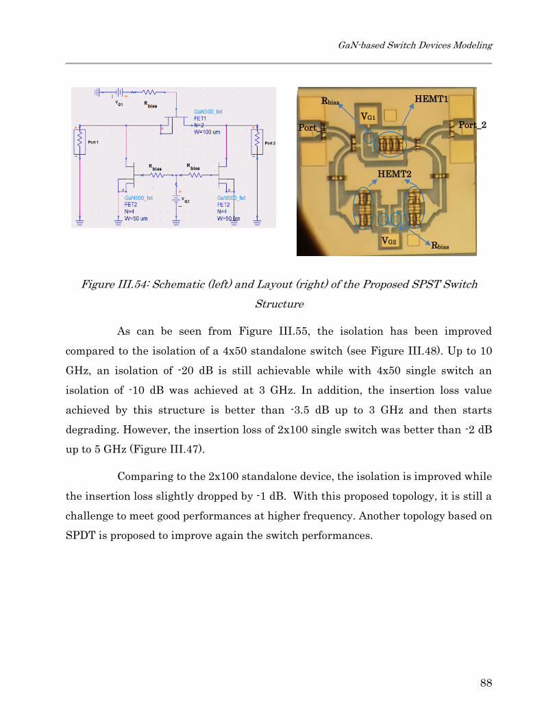
GaN-based Switch Devices Modeling
88
Figure III.54: Schematic (left) and Layout (right) of the Proposed SPST Switch
Structure
As can be seen from Figure III.55, the isolation has been improved
compared to the isolation of a 4x50 standalone switch (see Figure III.48). Up to 10
GHz, an isolation of -20 dB is still achievable while with 4x50 single switch an
isolation of -10 dB was achieved at 3 GHz. In addition, the insertion loss value
achieved by this structure is better than -3.5 dB up to 3 GHz and then starts
degrading. However, the insertion loss of 2x100 single switch was better than -2 dB
up to 5 GHz (Figure III.47).
Comparing to the 2x100 standalone device, the isolation is improved while
the insertion loss slightly dropped by -1 dB. With this proposed topology, it is still a
challenge to meet good performances at higher frequency. Another topology based on
SPDT is proposed to improve again the switch performances.
Port_1 Port_2
VG2
VG1
HEMT1
HEMT2
Rbias
Rbias

GaN Varactor and Switch Devices Modeling
89
Figure III.55: Measured SPST performances
3.3 SPDT Switch Structure
A SPDT switch topology is proposed in order to improve the isolation at
high frequencies. FETs are arranged in both series and shunt configurations. The
series FETs provide a through-path for the ON-state, while the shunt FETs provide
isolation for the OFF-state. The operation of the switch requires that series FETs and
shunt FETs associated with each switch state have opposite (or complementary)
conduction states and therefore opposite (or complementary) gate biases.
Figure III.56 illustrates the SPDT topology. If the Port_1 to Port_2 path is ON and
the Port_1 to Port_3 path is OFF, then FET1 and FET4 are biased ON, while FET2
and FET3 are biased OFF.
When the transistor FET1 as well as the FET4 are in the ON state
corresponding to VG1 = 0 V and VG2 = -5 V, FET1 behave as a small resistor which
allowing to the RF signal to go from port_1 to port_2. Verse-versa for the second state
when the signal is from port_1 to port_2
Freq [GHz]
[dB]

GaN-based Switch Devices Modeling
90
Figure III.56: Schematic (left) and Photograph (right) of the Proposed SPDT Switch
Structure
As was expected with this topology, some improvement in isolation is
achieved compared to SPST, while the insertion loss is increased by almost 1 dB. For
example, at 3 GHz an isolation of -25 dB and an insertion loss of -3 dB were achieved.
Unfortunately, the SPDT structure performances degrade with frequency. As we
hope to go higher in frequency, around 10 GHz, with these realized switch topologies
it will be impossible to achieve good performance. So, the SPDT structure which
presents good overall performances compared to SPST will be used in a beam
switched antenna system at 2.45GHz. At this frequency, an isolation better than -25
dB and an insertion loss of -3 dB are possible.
Due to the unavailability of having large signal equipment and also a RF
probe of type GSGSG to measure the outputs of the SPDT either at IETR (University
of Rennes 1) or DOE (Carleton University), we could not do the large signal
measurement of this structure. However, as will be presented in Chapter IV (Section
V), once this SPDT structure was mounted over a PCB by using wire-bonding
technique, the large signal measurement have been conducted and results are
presented and discussed in Chapter IV. In addition, by using ADS the SPDT small
Port_1
Port_2
Port_3
VG1
VG2
HEMT1
HEMT3
HEMT2
HEMT4

GaN Varactor and Switch Devices Modeling
91
signal model can be built based on the small signal model of a single standalone
switch. Here as shown in Figure III.57, only small signal measurements of this
structure are reported.
Figure III.57: Measured and Modeled Return Loss, Isolation, and Insertion Loss of
SPDT Switch Structure
Table III.8: Performances of the SPDT at the Marker m4
Performances Values
Modeled Insertion Loss -2.723 dB
Measured Insertion Loss -3.164 dB
Modeled Isolation -28.158 dB
Measured Isolation -25.937 dB
Modeled Return Loss -11.847 dB
Measured Return Loss -14.697 dB
Freq [GHz]
[dB]

Summary
92
IV. Summary
In this chapter, GaN HEMT-based varactor devices have been fully
characterized and modeled for the first time, showing limited usefulness for high
power applications due to their rapidly changing C-V characteristic. These GaN-
based varactors were designed in a standard GaN HEMT process, and were
fabricated with two different gate lengths, 0.5 µm (GaN500v1 and v2) and 0.15 µm
(GaN150v0). The varactor diode is realized by connecting together the drain and
source terminations thus resulting in a single Schottky junction which can be
considered as Planar Schottky Varactor Diodes (PSVDs). First of all, a small signal
analysis has been conducted and by analyzing the extracted CEq-VG curves,
mathematical expressions have been proposed to capture the nonlinear behavior that
can be used to represent a variety of different GaN based varactor sizes. These
equations maintain the simplicity of equivalent circuit modeling while offering good
agreement with measurements. In addition, an equivalent simple circuit model was
proposed and simulated, yielding good agreement between the simulated and the
measured results. The obtained Cmax/Cmin ratios and figures of merit compare
favorably with recently reported GaN varactors.
Secondly, a general large signal model for GaN varactor diodes
manufactured with gate lengths of 0.5 µm (GaN500v2) has been presented. This
model is based on an analytic expression which describes the Ceq-VG curve and has
shown to maintain a high level of accuracy, well into the large power range up to 18
dBm. In addition, the proposed circuit model in small signal analysis is always valid
for large signal by considering the new analytical equation of CEq versus the input
power (Pin.) With reverse bias and RF power level included in the model, the junction
capacitance ratio (CMAX/CMIN) of the realized varactors was shown to be decreased
from 1.73 to 1.25. This ratio can be much further decreased, if the RF power level is
increased further. From the presented results and given GaN’s high breakdown
voltage, these varactors would be very useful in various applications in receive mode,

GaN Varactor and Switch Devices Modeling
93
where power limiters could be completely excluded as protection circuitry from
jammer signals.
Finally, in this chapter, different sizes single standalone switches and
switch structures such as SPST and SPDT were fabricated and presented. As
mentioned, only small signal measurement were reported. It was observed that, with
single transistor in common gate configuration, the isolation is good at low
frequencies but quickly drops with increasing frequency. In addition, it was observed
that more the device is large, lower the insertion loss is achieved but poorer the
isolation will be. A trade-off between insertion loss and isolation has been made to
choose the single transistors that will be used for designing switch structures such as
SPST and SPDT which could improve the performances at high frequencies.
Comparing to the standalone device, it was revealed that with SPST structure, the
isolation is improved while the insertion loss slightly dropped by -1 dB. With this
proposed topology, it is still a challenge to meet good performance at our higher
frequency. Another topology based on SPDT was proposed to improve more the
performances. As was expected with this topology, some improvement in isolation is
achieved compared to SPST, while the insertion loss is increased by almost -1 dB. For
example, at 2.45 GHz (frequency of interest) isolation better than -25 dB and an
insertion loss of -3 dB were achieved. However, the SPDT structure performances
degrade with frequency. Moreover, based on these small signal measurements, a
model was introduced. It was observed that this linear model is the same to the one
proposed in [[90] by Tyler Ross using GaN500v1 from NRC foundry. In addition, the
fabricated SPDT switch structure will be integrated with antenna system to realize
and to demonstrate the ability of using GaN devices for a beam switching antenna
array.

Introduction
94
Chapter IV
---------------------------------------------------------------------------------------------------------------------
Realized GaN-Based Reconfigurable
Circuits
I. Introduction
As a result of the emerging need for multi-band and multi-services
requirements within a single design structure, the electronically tunable or
reconfigurable devices have experienced [92], over the last years, with a significant
growth in radio frequency (RF)/Microwave wireless front-end applications such as
antennas, power amplifier, phase-shifters, oscillators and filters. Moreover, this has
been the modern trends in technological of the new compact-structured RF
transceivers [93].
Also, the use of wireless devices has increased dramatically over the last
years. This increased utilization has led to a need for more efficiency RF circuits with

Realized GaN-Based Reconfigurable Circuits
95
more functionalities. Therefore, the continuing demands for highly portable, more
reliable and more power efficient, low cost wireless systems require that future
wireless devices must be compatible with different communication protocols and
capable of operating over a wide frequency range. Furthermore, applications of such
systems in personal and satellite communications impose the specifications for
circuits miniaturized in size and weight. Thus, as wireless devices become more and
more compact, the appeal of reconfigurable circuits is that they can decrease the
number of components with identical specifications, decrease the number of
input/output pins, reduce the size of the integrated circuit area, and reduce power
consumption [94].
Tunable devices with a high performance are, also, more crucial for mobile
devices and are for selective applications. Generally, an adaptive RF circuit must
have the capabilities to handle different functionalities such as signal routing,
impedance matching agility, adjustable gain amplification, tunable phase shifting
[95], etc. In contrast, a tunable circuit with embedded tuning elements can carry out
a switching function of several parallel circuits with a simple change to one of the
elements. Figure III.1 illustrates this example for the case of duplexers in a tri-band
system where a single tunable duplexer can replace three fixed duplexers [96].
Figure IV.1: (left) Tri-band system with three fixed duplexers and (right) with a
single tunable duplexer [96]

Introduction
96
Comparing the above architectures, a single tunable duplexer offers higher
flexibility, more functionalities, lighter weight and denser integration. In addition,
such a circuit tuning allows an easier controlling of systems through baseband signal
processing, which can add attractive features of smartness of combined multi-
services. Therefore, it is obvious that due to the convergence towards the integration
of multiple standards and services into a single circuit and maintaining their
expected performances at various configuration parameters, wireless systems are
becoming more complex and highly smart.
Depending on the specific RF design where reconfigurable components are
suitable, the result may be a saving in cost, reduction in size, better performance,
and/or increased functionality. In order to implement these electronically
reconfigurable components, there are currently various main techniques [95] that
could be listed as follow:
Ferrite materials
Ferroelectric technology
Semiconductor varactor diodes or switches
Micro-electromechanical systems MEMS
During the last years, Monolithic Microwave Integrated Circuits (MMICs)
based on semiconductors technology have become more attractive for electronic
reconfigurability due to their small size, easiness integrations, possibly to be mass-
produced, etc. Most MMICs currently in production, such as GaAs, SiC, InP, etc,
operate in the microwave and mm-w range with modest breakdown voltage and
limited power handling capabilities. But there are increasing applications in the
RF/microwave spectrum with higher power requirement.
As already presented in chapter II, GaN technology can be ideal for the
design of high power devices for microwave and mm-w applications. In-depth
research studies have been conducted to explore the performance of GaN technology,
as well as reconfigurable RF/microwave circuits using GaN devices [97]. GaN HEMTs

Realized GaN-Based Reconfigurable Circuits
97
semiconductor devices are no longer limited to RF power amplifier applications,
having been emerged to other applications such as LNAs, VCOs, mixers, and phase
shifters.
For the above mentioned strong points of reconfigurable components, GaN
technology can be considered as a real promising candidate semiconductors
technology, capable of significantly reducing the number of components with identical
specifications, size and cost of devices utilized in transmitter and receiver chains of
front-end modules used in RF/microwave systems.
II. Tunable Phase Shifters
1. Review
Phase shifters are important components that find their use in many
RF/microwave systems. For example, they can be used in electronic beam-scanning
phased arrays, microwave instrumentation and measurement systems, power
divider, and as modulators [97] in communication sub-systems.
Phase shifters can be analog or digital. Analog phase shifters provide a
continuously variable phase, which can be controlled by a voltage. Electronically
controlled analog phase shifters can be realized with varactor diodes that change
capacitance with voltage, or nonlinear dielectrics. In the other hand, digital phase
shifters provide a discrete set of phase states that are controlled by two-state "phase
bits". They are characterized by a certain number of bits. This number defines
straightforwardly the achieved phase. More bits there are, smaller phase step will be.
For example, a five bits phase shifter would have a 11.25°(=360°
25 𝑏𝑖𝑡𝑠) as a phase shift
step. This means that each bit allows to get a phase shift successively over 11.25°,
22.5°, 45°, 90° and 180°.

Tunable Phase Shifters
98
There are various design parameters that should be considered such as
frequency range, total phase variance (Δϕ), phase resolution, insertion loss,
bandwidth, return loss, harmonics level, power handling and design area. This makes
some challenges in the design and optimization of integrated phase shifters. In
addition, there are five main phase shifter topologies and described as follow [98]:
Switched line phase shifter
Loaded line phase shifter
Reflection type phase shifter
All pass network phase shifter
High Pass / Low Pass phase shifter
As highlighted in the PhD dissertation [[30] about GaN phase shifters, if
phase shifters are implemented in a low power semiconductor technology, such as Si
or GaAs, it may have to be placed in transmit and receive chains in RF front-end
system, where it will not be damaged by large signals in any unexpected situation,
thus resulting in relatively high cost and low integration density. Figure IV.2 shows
a simplified RF front-end for a beamforming system. However, with recent
developments in high power technology semiconductors such as GaN, it is possible to
design phase shifters that can simplify the front-end system and make it more
efficiently. An example of this is shown in Figure IV.3. Since the active devices in the
phase shifter can handle both weak and strong signals, the circuit will operate
properly and will not be damaged. As it is in the common path, only one phase shifter
per antenna element is required as well, and the transceiver component count and
cost can be drastically reduced. GaN-based Phase shifter with good high power
handling and low loss hold the key to realize an affordable electronically steerable
system, eliminating the need for active transceiver modules at every element.

Realized GaN-Based Reconfigurable Circuits
99
Figure IV.2: Simplified RF front-end for a typical beamforming system in a non-
GaN technology [[30]
Figure IV.3: Example RF front-end possible with GaN with key components in blue
[[30]
While there has been significant progress made in developing GaN
technology for high-power amplification applications as explained before in Chapter
II, there have been few studies to date on the use of GaN HEMTs for high-power
RF/microwave phase shifters applications. In future RF/microwave systems that are
based on GaN device technology, the GaN control elements, such as phase shifters,
will often be conjointly placed together with high-power GaN amplifiers, thereby
requiring an in-depth look at these control devices in term of their parameters design
presented previously.

Tunable Phase Shifters
100
Using GaN technology, a few phase shifters works have already been
reported over the last few years. A new type of GaN HEMT based high power shifter
at X-band permitting to switch between two states [99] was reported for the first time
by a research group from Carleton University. As shown in Figure IV.4, this work is
based on the high-pass/low-pass phase shifter or T-topology which has original
advantage such as its superior power and phase-bandwidth capabilities compared
with more conventional switched line, reflection, or loaded line phase shifters. As
illustrated, the proposed phase shifter consists of two SPDT switches, a low pass
network, and a high pass network. The 0°/45° signal shift is achieved by switching
between two filters, low pass and high pass networks. As shown in Figure IV.5 and
Figure IV.6, where measured results are depicted, the proposed 0°/45° high-pass/low-
pass phase shifter exhibits low insertion loss (2.5 dB), good return loss, and amplitude
variation lower than 0.5 dB for the two phase states over the entire operational
bandwidth ranging from 6 to 13 GHz, while the measured phase difference between
the two states varies from 45º to 55º over the design frequency range of 8–12 GHz (see
Figure IV.7). This work has been demonstrated by using a 0.8 μm gate GaN HEMT
process from NRC foundry which is the first GaN HEMTs NRC developed process.
Figure IV.4: Photograph of a novel GaN HEMT based high power high-pass/low-
pass phase shifter [99]

Realized GaN-Based Reconfigurable Circuits
101
Figure IV.5: Measured insertion and return loss for high pass [99]
Figure IV.6: Measured insertion and return loss for low pass [99]
Figure IV.7: Measured phase difference between the two states [99]

Tunable Phase Shifters
102
Later on 2014, the same authors have reported a novel high power X-band
GaN phase shifter [100] based on switched-filter configuration by using a novel
developed NRC GaN fabrication process which is a 0.5 μm gate width. The use of this
topology is widely found useful when compact circuits are required because less chip
area is required compared with other phase shifter topologies. Figure IV.8 shows a
microphotograph of the designed phase shifter. The manufactured 0°/22.5° switched
filter phase shifter has much wider bandwidth covering 8-16 GHz, while maintaining
low insertion loss of 2 dB, good return loss > 11.15 dB and an amplitude imbalance of
less than 1.03 dB across X-band. Figure IV.9 presents the obtained phase shift while
the measurements of linearity and power handling capability of the circuit are
depicted in Figure IV.10. With the 0° (bypass) state, the measured IIP3 was 46.2 dBm
while for the 22.5° phase shift state had a higher IIP3 of 50.4 dBm. The obtained 1
dB compression point is well over 40 dBm.
Figure IV.8: Microphotograph of the 0°/22.5° GaN switched-filter phase shifter [100]

Realized GaN-Based Reconfigurable Circuits
103
Figure IV.9: Measured and simulated phase shift [100]
Figure IV.10: Linearity measurement [100]
Using the topology presented in [[30], an analog phase shifter using GaN
Schottky diode is reported in [101] for 35 GHz operation. This design reports
fabrication and experimental characteristics of a 35 GHz MMIC analog phase shifter
using GaN Schottky diodes to enable continuous phase shifting. Figure IV.11 shows
the schematic and photograph of the designed T-phase shifter. The reported design
contains two series connected diodes and another diode in the shunt arm which is
connected to a spiral inductor to achieve the optimum matching and phase shifting
at 35 GHz. The phase shifter presents analog phase shifting capability up to 45° with
∼ 7 dB insertion loss and a return loss of -10 dB in the 32 to 38 GHz range as

Tunable Phase Shifters
104
illustrated in Figure IV.12. Good power handling capability and robust performance
is demonstrated through large signal analysis and experimental characterization as
explained in this paper.
Figure IV.11: T-Phase shifter Circuit Configuration and microscope image [101]
Figure IV.12: Phase shift of the high-pass T-network and the corresponding
inductance for 50 Ω impedance matching [101]

Realized GaN-Based Reconfigurable Circuits
105
Figure IV.13: phase shift of the T-Phase shifter in the frequency range of 32 GHz to
38 GHz [101]
2. Design of Analog GaN-based Phase Shifter
Analog phase shifter based varactor diodes structure is, first of all, very
simple to design. Secondly, compared to a digital MMIC phase shifter, the power
consumption is low and only a single input control voltage is required. Additionally,
a continuous phase shift is easily achievable, thus allowing to provide any desired
phase shift. Among the more useful topologies for analog phase shifters are the loaded
line structure and the reflective structure employing quadrature 3-dB 90° hybrid
coupler using either lumped or distributed elements with two reflective loads at
terminations. One of the major drawbacks of reflection phase shifter structure is that
the overall insertion loss of the circuit is usually high. These insertion losses are
especially related to the equivalent series resistor presented by the used varactor and
also the coupler’s elements.
Using the first commercialized NRC GaN150v0 HEMTs process, a phase
shifter based on quadrature reflection structure was designed and simulated using
ADS Agilent simulator, along with the development of the reported small signal GaN

Tunable Phase Shifters
106
varactor diodes model. Here this developed GaN varactor diode, already presented in
Chapter III, is used as tuning load purpose. Moreover, at least two varactor diodes
are required to achieve a theoretical phase shift of 180° [102], making the device
smaller and less expensive to fabricate compared to digital phase shifter; and the
diodes are operated at reverse bias, having very fast response times and requiring
voltage but no current consumption.
It is highly import to keep in mind that, to the author knowledge’s, this the
first developed GaN phase shifter based on quadrature reflection structure even if
only simulation results will be presented.
Here, before presented the simulated results, a description of how this
phase shifter structure works is giving. As shown in Figure IV.14 and Figure IV.15,
basically, a phase shifter based reflection structure consists of a quadrature hybrid
coupler that splits the incident signal into two separate signals of equal amplitude
and 90° phase difference over the two opposite ports (2 and 3), while isolating the
adjacent one (port 4). These two signals reflect from the two tunable loads, GaN
varactors connected to the coupled and thru ports of the hybrid, and add up in phase
at the hybrid’s isolated port if both of the loads are identical, and will ideally be
isolated from the phase shifter’s input signal. This means that the voltage at the
output port can be written as [103]:
Equation (9)
𝑉𝑜𝑢𝑡 = 𝑗. Г. 𝑉𝑖𝑛
Equation (10)
Г = |Г|. 𝑒−𝑗𝜙
The phase angle, 𝜙, of the reflection coefficient, Г, can be varied by
changing the capacitance of the loading varactor diodes which are controlled by DC
voltage and, theoretically, have to present a pure imaginary impedance. While |Γ|

Realized GaN-Based Reconfigurable Circuits
107
must be unchanged and equal to 1 in order to not introduce any additional loss into
the phase shifter. Practically, it is impossible to achieve perfect reflection from a load
which means that some power will be dissipated in the load and |Γ| will be less than
one. Therefore, some loss will always occur between the input and output signals. By
inserting varactors in the terminations, a continuous control of the phase shift is
achieved in this manner.
Figure IV.14: Phase shifter based on 3-dB/90 branch-line hybrid coupler using
distributed elements
Figure IV.15: Phase shifter based on 3-dB/90 branch-line hybrid coupler using
lumped elements
Zr
Zp

Tunable Phase Shifters
108
To design this phase shifter topology, firstly, a 3-dB 90° hybrid coupler has
been designed and simulated. The simulated results will be discussed later in this
section. Then, the two coupler’s outputs ports have been loaded by GaN varactors.
The final phase shifter design presented in this section was designed and
were planned to be manufactured by using GaN150v1 process. However, due to
factors beyond our control, fabrication of this phase shifter at the CPFC-NRC could
not proceed as planned. The design was planned to be submitted for fabrication on
7th September, 2015 and then four months later samples should be delivered. Since
this design was the only application for 2x2mm2 space in this run fabrication
referenced as “1503GK” that cost $70K/run and because it is outside of our funds to
purchase the entire run. The number of participants is not enough so the run of
manufacturing has been completely cancelled. Due to this unexpected fabrication
issue, only simulation results and design steps will be reported here
2.1 Quadrature 3-dB 90° Hybrid Coupler
Quadrature 3-dB 90° hybrid couplers are usually realized in some type of
microstrip or stripline technology using distributed quarter-wavelength (λ/4)
transmission lines (see Figure IV.14). They have been extensively progressed because
of their good bandwidth of operation and of its straightforward design and reliability.
However, this design approach could require several mm2 of area to be realized and
renders their size relatively large even for mm-wave frequencies due to the length of
λ/4 lines [104]. Thus it would consume considerable wafer space of the used
semiconductor technology, and the design size gets much larger. Additionally, the
most important issue of the distributed λ/4 hybrid coupler in MMIC applications is
the chip area which is directly related to the chip cost. Also the most significant
challenge when dealing with a priced semiconductor technology especially GaN
HFET technology is the high expense costs for technology access. Hence, there have

Realized GaN-Based Reconfigurable Circuits
109
been several attempts to reduce the size of coupled line coupler, the most important
alternative solution is to use lumped elements instead of resonant λ/4 transmission
lines [104]. However, the bandwidth of the structure hybrid coupler is usually
narrower than that of the typical λ/4 structure. Another issue comes up is that this
structure becomes inefficient at high frequency (i.e mm-w) because of the inductors
become very lossy and also tend to resonate at frequencies very close to the operating
frequencies.
In this approach, the quarter-wave lines are approximated at operating
frequency with lumped elements as depicted in Figure IV.15. Theatrically, the ABCD
matrix of a single segment representing a perfect transmission line characterized by
a characteristic impedance of Zr is written as follow:
Equation (11)
Cos SinZr
1j
jZrSin Cos
D C
BA
The equivalent of this matrix by using lumped elements can be written as follow:
Equation (12)
11²1 ²L1C1)-C1(2j
L1j 11²1
1 C1j
0 1
1 0
L1j 1
1 C1j
0 1
D C
BA
CL
CL
From Equation (11) and Equation (12), we can drive the following
equations:
Equation (13)
11²1 Cos CL

Tunable Phase Shifters
110
Equation (14)
L1 ZrSin
Equation (15)
²L1C1)-C1(2SinZr
1
The combining between Equation 14 and Equation 15 gives the following
equation:
Equation (16)
²)1(-L1
C12
Zr
1C
So the passive elements, L1 and C1, of the hybrid coupler can be calculated
by the following driven equations:
Equation (17)
ZrSin1L
Equation (18)
cos1
cos1
Zr
11
C
By using the same previous procedures, the other passives elements, L2
and C2, can be, also, calculated as follow:
Equation (19)

Realized GaN-Based Reconfigurable Circuits
111
ZpSin2 L
Equation (20)
cos1
cos1
Zp
12
C
So these previous equations give theoretically first guess values of the
lumped elements of hybrid coupler.
Based on this topology, we report here a simulation analysis of a new fully
embedded lumped element GaN MMIC 3-dB/90° hybrid coupler at X-band that it will
be later used to conduct an analysis of a phase shifter design. A three-dimensional
layout view of the coupler, showing embedded metal and vias layers, of the designed
coupler is displayed in Figure IV.20.
The built block of the 3-dB/90° hybrid coupler using lumped spiral
inductors and metal-insulator-metal (MIM) capacitors is very small in size
(0.85x1mm2). It consists of lumped multi-turn spiral inductors and MIM capacitors
from NRC GaN150 PDK components library [105]. The mutually coupled inductors
turns are rectangular spiral inductor type and are implemented with reinforced
between two metals, metal 2 (2ME) on metal 1 (1ME) by using via connection (VIA2),
which results in an inductor having a higher Q-factor and size reducing. The current
carrying capability of this inductor is limited by the width of the air-bridges. Higher
currents can be sustained by increasing the width of the air-bridges, with a
commensurate increase in the gap spacing between the inductor turns. A sample
layout for a square inductor is shown in Figure IV.16, while in Figure IV.17 an
inductor equivalent circuit is presented which is used to estimate the inductance (LS),
series resistance (RS) and first resonance frequency FRES.
The MIM capacitors are formed by 2ME on top of 1ME without a VIA2
connection. A layer of silicon nitride, also used to provide insulation, is used as the

Tunable Phase Shifters
112
dielectric layer. The dielectric constant of the silicon nitride is 6.5 and the thickness
is 0.3um [105]. The capacitance density of the MIM structure is 0.19 fF/µm2.
Figure IV.19 illustrates the capacitor layout.
At 10 GHz, the optimized values of the four lumped elements, L1, L2, C1
and C2, constituting the hybrid coupler are, respectively, 6.7 nH, 8.45 nH, 369 fF and
136 fF. These values, firstly, have been determined by using the above equations
(Equation (17, Equation (18, Equation (19 and Equation (20) and then have been
optimized in ADS to achievegood performances. So, these values are corresponding to
parameters presented in Table IV.1 and Table IV.2.
Table IV.1: Optimized Values of Inductors L1 and L2
Inductor L1 Inductor L2
Value (nH) 6.7 8.45
Ns (turns) 10 10
L1 (µm) 120 155
L2 (µm) 125 125
L3 (µm) 110 135
Ln (µm) 20 20
W (µm) 15 15
S (µm) 5 5
Wb (µm) 10 10
Ab 90 90
Be (µm) 30 30
Table IV.2: Optimized Values of Capacitors C1 and C2
Capacitor C1 Capacitor C2
Value (fF) 369 136
W (µm) 43.86 26.63
L (µm) 43.86 26.63
Wc (µm) 15 10

Realized GaN-Based Reconfigurable Circuits
113
Figure IV.16: Layout of a Spiral Inductor Generated from NRC GaN150 PDK [105]
Figure IV.17: An Equivalent Circuit to Estimate LS, RS and Fres [105]
Figure IV.18: Layout of A MIM Capacitor [105]

Tunable Phase Shifters
114
For the presented hybrid coupler, as indicated in Figure IV.19, port 1 is
designed as the input port, port 2 as the transmitted port, port 3 the coupled port and
port 4 the isolated port. Since this is a symmetrical network, any port can be used as
the input port and the function of the other ports appropriately defined. Through
wafer vias (TWV) are used for connection to the backside ground wafer metal. The
ports 1 and 4 consist of G-S-G pads that have a pitch of 150 μm to be compatible with
RF probes of the same geometry.
Figure IV.19: Layout of the designed hybrid coupler

Realized GaN-Based Reconfigurable Circuits
115
Figure IV.20: 3-D Layout view of the designed hybrid coupler
2.1.1. Simulated Results and Discussion
The ADS co-simulated layout results for the complete hybrid coupler are
plotted in Figures from Figure IV.21 to Figure IV.24. The insertion loss at port 2 and
port 3 are -0.7 dB at 10 GHz and has a maximum variation of -0.4 dB over a 1 GHz
bandwidth (see Figure IV.21). The amplitude imbalance at the center frequency is
almost 0 dB. The phase difference (see Figure IV.24) between the outputs of ports 2
and 3 is about 89.5° at 10 GHz and varies by only 0.5° over a 1 GHz bandwidth. The
return loss is better than -20dB at 10GHz (see Figure IV.22) and the isolation
between the ports is better than -35dB (see Figure IV.23).
This compact 3-dB 90° GaN MMIC hybrid coupler based on lumped
elements has been successfully designed by using NRC GaN150v1 process. The
advantages of size reduction and good performance of the proposed 3-dB 90° hybrid
coupler at X-band have been confirmed through the simulated results. Comparing to
a reported GaAs hybrid coupler using distrubuted elements [106] with a size of
3.1x2.3mm2, this design (size of 0.85x1mm2) has shown a size reduction of 70 % in
the circuit area at 10 GHz. These results indicate that the proposed hybrid coupler is
very promising for high density and tunable MMIC applications. Moreover, the
hybrid coupler is used for designing a highly miniaturized and tunable phase shifter.
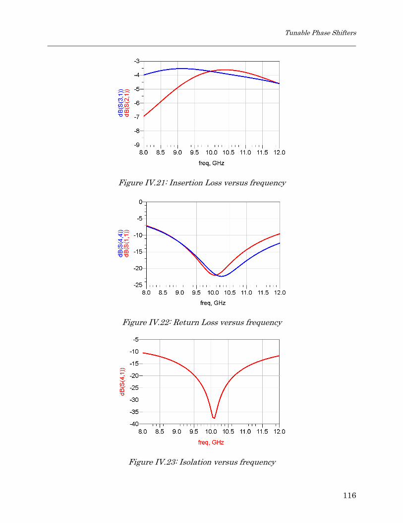
Tunable Phase Shifters
116
Figure IV.21: Insertion Loss versus frequency
Figure IV.22: Return Loss versus frequency
Figure IV.23: Isolation versus frequency

Realized GaN-Based Reconfigurable Circuits
117
Figure IV.24: Phase Shift Difference versus frequency
2.2 Phase Shifter Design
As previously stated, the developed hybrid coupler will be used to design a
phase shifter. This section discusses the design analysis of X-band GaN-based phase
shifter. As depicted in Figure IV.25 and Figure IV.26, a layout photo as well as a 3-D
view of the phase shifter are presented.
Here two identical GaN varactors were used as tuning loads purpose and
placed at the transmitted and coupled ports of the hybrid coupler. These devices have
a gate width of 200μm and two fingers for each. The actual used GaN device model
is scaled from the two characterized original gate width GaN devices of 50μm and
100µm model described previously in Chapter III. DC biasing is provided to the GaN
varactors via DC probes with external bias tees. The circuit was simulated in
Agilent’s Advanced Design System (ADS) and Momentum was used to model the
passive circuitry. The circuit was optimized to provide a maximum continuous phase
shift at 10 GHz.

Tunable Phase Shifters
118
Figure IV.25: Layout of the designed Phase Shifter
Figure IV.26: 3-D Layout view of the designed Phase Shifter

Realized GaN-Based Reconfigurable Circuits
119
2.1.2. Simulated Results and Discussion
In Figure IV.27, the return loss of the phase shifter under different bias
conditions is presented and is better than 20 dB across a 1 GHz bandwidth centered
at 10 GHz. As clearly can be seen, a good match is achievable over this range of 9.5–
10.5 GHz for all bias point varying from -3.5 V to -5.5 V which corresponding to the
tuning range of the developed GaN varactor as stated previously in Chapter III.
Figure IV.28 shows the insertion loss of the phase shifter in different bias
level from -3.5 V to -5.5 V. At 10 GHz worst case of the insertion loss is about -3 dB
and occurs at a bias point of -4.3 V. This value could be due to the higher series
resistor value, 9 Ω, of the used varactor (i.e W100L0.15) at this bias voltage as
reported in Chapter III (see Figure III.26). The amplitude imbalance between the two
extreme DC bias states (i.e -3.5 V and -5.5 V) is about 1.07 dB at 10 GHz, and is
therefore better than 1.2 dB over the extended band from 9.5 to 10.5 GHz.
Figure IV.29 presents the phase shift obtained from the circuit versus DC
bias at 10 GHz. Therefore, a continuously variable phase-shift range of 80° is
achieved as shown. This phase shift range versus DC bias exhibits the same general
behavior as for equivalent capacitor of varactor versus DC bias as discussed in
Chapter III in Figure III.24, which can be separated into three regions: range (1) for
VG above -3.5 V corresponding to the minimum phase shift value (-80°), range (3) for
VG < -5 V corresponding to the maximum phase shift value (0°) and range (2) for -5 V
≤ VG ≤ -3.5 V where the phase shift values change significantly and rapidly.
Maximum loss figure-of-merit (FOM) of this phase shifter of 74.76°/dB at
10 GHz and 66.66°/dB in the range of 9.5 –10.5 GHz were achieved. The loss FOM
can be expressed as:
Equation (21)
𝐹𝑂𝑀= |𝛥𝜙|(°)
αmax(𝑑𝐵)
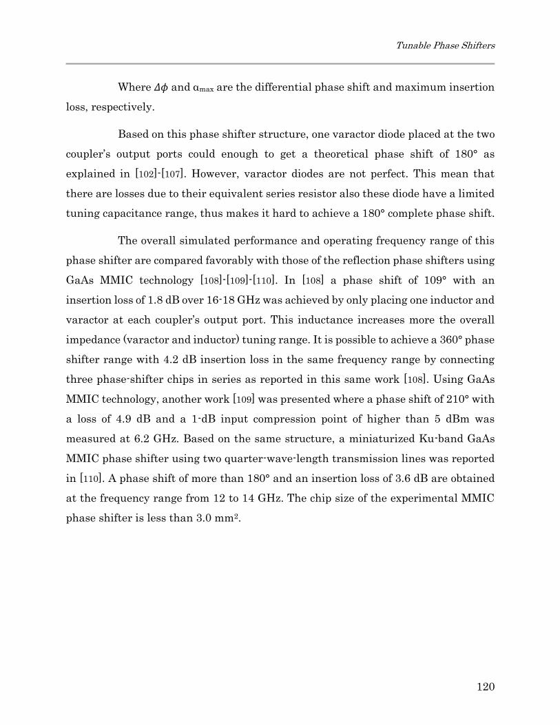
Tunable Phase Shifters
120
Where 𝛥𝜙 and αmax are the differential phase shift and maximum insertion
loss, respectively.
Based on this phase shifter structure, one varactor diode placed at the two
coupler’s output ports could enough to get a theoretical phase shift of 180° as
explained in [102]-[107]. However, varactor diodes are not perfect. This mean that
there are losses due to their equivalent series resistor also these diode have a limited
tuning capacitance range, thus makes it hard to achieve a 180° complete phase shift.
The overall simulated performance and operating frequency range of this
phase shifter are compared favorably with those of the reflection phase shifters using
GaAs MMIC technology [108]-[109]-[110]. In [108] a phase shift of 109° with an
insertion loss of 1.8 dB over 16-18 GHz was achieved by only placing one inductor and
varactor at each coupler’s output port. This inductance increases more the overall
impedance (varactor and inductor) tuning range. It is possible to achieve a 360° phase
shifter range with 4.2 dB insertion loss in the same frequency range by connecting
three phase-shifter chips in series as reported in this same work [108]. Using GaAs
MMIC technology, another work [109] was presented where a phase shift of 210° with
a loss of 4.9 dB and a 1-dB input compression point of higher than 5 dBm was
measured at 6.2 GHz. Based on the same structure, a miniaturized Ku-band GaAs
MMIC phase shifter using two quarter-wave-length transmission lines was reported
in [110]. A phase shift of more than 180° and an insertion loss of 3.6 dB are obtained
at the frequency range from 12 to 14 GHz. The chip size of the experimental MMIC
phase shifter is less than 3.0 mm2.

Realized GaN-Based Reconfigurable Circuits
121
Figure IV.27: Return Loss at several DC Bias from -3.5 V to -5.5 V
Figure IV.28: Insertion Loss of the Phase Shifter at several DC Bias from -3.5 V to -
5.5 V
Figure IV.29: Phase Shift versus DC Bias at 10 GHz

GaN Reconfigurable 3-dB/90 Hybrid Coupler
122
In this section, a GaN phase shifter design based on reflective topology has
been presented for high RF power source application. First, the 3-dB 90° hybrid
coupler has been designed and simulated using NRC GaN150 PDK. Then two
developed GaN varactors were paced on the two coupler’s output ports as loads.
Under different bias conditions varying from -3.5 V to -5.5 V, the return
loss of the phase shifter is better than 20 dB across a 1 GHz bandwidth centered at
10 GHz, while good match is achievable over this range of 9.5–10.5 GHz. Worst case
of the insertion loss is about -3 dB at 10 GHz and occurs at a bias point of -4.3 V where
the equivalent resistor of the used varactors is significantly high. Therefore, a
continuously variable phase-shift range of 80° is achieved at 10 GHz. These achieved
performances were compared favorably with other works that use GaAs technology.
III. GaN Reconfigurable 3-dB/90° Hybrid Coupler
1. Review
Based on the previous presented 10 GHz GaN hybrid coupler, a frequency
reconfigurable 3-dB 90° hybrid coupler is designed. In order to achieve frequency
reconfigurability, varactors diodes are used instead of the four fixed shunt lumped
capacitors C1 of the previous static frequency hybrid coupler (see Figure IV.19). In
this configuration, an electronically frequency tuned is achieved by changing the bias
voltage applied across the varactors. This means that changing the resonance
frequency of branch-line (LC parallel resonator) hybrid of the coupler, we can provide
the different operating frequency bands. Additionally, the tuned frequency of the
coupler is defined as the frequency at which high isolation and low return loss are
achieved, while realizing phase shift of 90° between the isolated and the coupled
ports. The novel tunable GaN hybrid coupler employs the developed GaN varactors
elements to provide the reconfigurability from 10 GHz to 16 GHz.

Realized GaN-Based Reconfigurable Circuits
123
Recently, considerable work in tunable couplers consist of MMIC-based
active couplers and varactor diode based passive couplers have been reported in the
literature which most of them are operating below X-band frequency. However, most
of these reported couplers exhibit, in general, a small frequency tuning range. It is
still a challenging task to design tunable couplers with tuning ranges wide enough to
cover desired frequency bands. For instance, in [111] a tunable hydrid coupler is
reported using GaAs technology. This presented tunable GaAs MMIC directional
coupler design uses tunable capacitances to achieve a tunable coupling coefficient
(|S31|) at 2 GHz. Over a bias range of 0 V to -1.5 V the measured S-parameters for
the coupled port demonstrate a tuning range of -6.6 dB to -60 dB. The input return
loss is better than -12 dB for all bias voltage levels with isolation better than -17 dB.
This design is implemented in a 0.5 µm GaAs process with Schottky varactor diodes,
and occupies an area of 2.2× 1.4mm2. In [112] a frequency tunable broadband MMIC
active directional coupler is discussed. The coupler provides various coupling gains
such as 3 dB, 0 dB, -3 dB, and -6 dB, also a tuned frequency from 5.5 GHz to 7.8 GHz
was achieved by applying different bias voltages. Using varactors for tunability
purpose, a novel compact dual-band reconfigurable power divider is presented in [113]
for smart antenna applications. Measured results show that, by biasing one varactor
and keeping the other one at 0V, good performance are achieved at the center
frequency 2.45 GHz, while this frequency can be tuned to 5.25 GHz by only switching
the bias state of varactors. Also, any value of power ratio can be selected from 1:0 to
0:1 for both the center frequencies 2.45 GHz and 5.25 GHz, maintaining an average
insertion loss better than -1.5 dB and -3 dB in the 2.45 GHz and 5.25 GHz bands,
respectively, along with a return loss better than -15 dB in both frequency ranges.
Measured isolation at port 2 is always better than -20 dB in both frequencies.

GaN Reconfigurable 3-dB/90 Hybrid Coupler
124
2. Design of Reconfigurable 3-dB/90° Coupler
In this context, here we report a continuous broadband frequency tunable
GaN hybrid coupler. The achieved tuning range is from 10 GHz to 16 GHz
corresponding to a bandwidth of 46%. As far as the authors know, this proposed
frequency reconfigurable hybrid coupler is the first reported work that uses GaN
HEMTs technology. Figure IV.30 and Figure IV.31 show the tunable layout design
version of the coupler, where the shunt MIM capacitors are replaced by the developed
GaN varactors model. The varactors provide the function of frequency tunability by
adjusting their voltage level. This varactor device, W200L0.15, is a two fingers and
200 um gate length and is fabricated using GaN150 process.
Figure IV.30: Layout of the designed hybrid coupler

Realized GaN-Based Reconfigurable Circuits
125
Figure IV.31: 3-D Layout view of the designed hybrid coupler
2.1 Simulated Results and Discussion
Simulation results, which are shown in Figure IV.32, Figure IV.33,
Figure IV.34, Figure IV.35 and Figure IV.36, respectively, are illustrating, at several
DC level voltage for return loss, isolation, power division at transmitted port and loss
insertion at coupled port.
The overall return loss depicted in Figure IV.32 is better than -13.5 dB over
all the tuning range from -3.7 V to -4.8 V. This worst case of -13.5 dB is achieved at a
DC bias of -3.7 V corresponding to the maximum value of varactor capacitance. In
Figure IV.33, the isolation is clearly below than -14 dB over the full tuning range.
The simulated magnitude of S21 parameter, as illustrated in Figure IV.34,
is close to -3.5 dB and is getting poorer as varactor capacitance values decreases. A
worst value of -5 dB is achieved at the minimum capacitance value. While at port 3,
the S31 parameter (see Figure IV.35) behaves as S21 but in a reverse way. This
means the worst case which is about -3.7 dB achieved when the varactor capacitance

GaN Reconfigurable 3-dB/90 Hybrid Coupler
126
is at its maximum. As a result, the amplitude imbalance is varying from -0.2 dB at
10 GHz and -2 dB at 16 GHz.
A minimum well-balanced quadrature phase of 86.5° is obtained between
the coupled port 2 and the through port 3 as plotted in Figure IV.36. This phase is
increasing and getting closer to 90 ° as varactor capacitor values are decreasing. The
tunable quadrature coupler has 46% center-frequency tunable range from
approximately 10 to 16 GHz.
There are four DC blocking capacitors on each port to block the DC bias
from the output. This simplified bias network aids in reducing the overall size and
complexity of the circuit.
Unfortunately, as for the phase shifter, this design has not been
manufactured because the run of manufacturing on GaN150 process has not been
done in time by NRC.
Figure IV.32: Return Loss at several DC Bias from -3.7 V to -4.8 V

Realized GaN-Based Reconfigurable Circuits
127
Figure IV.33: Isolation at several DC Bias from -3.7 V to -4.8 V
Figure IV.34: Level of S21 at several DC Bias from -3.7 V to -4.8 V
Figure IV.35: Level of S31 at several DC Bias from -3.7 V to -4.8 V

GaN Reconfigurable 3-dB/90 Hybrid Coupler
128
Figure IV.36: Phase Difference at several DC Bias from -3.7 V to -4.8 V
A varactor tunable broadband quadrature hybrid coupler has been
investigated and simulated from X-band to Ku-band frequencies applications. First,
a static coupler has been designed to meet the specifications of a typical quadrature
hybrid coupler (3-dB insertion loss, good return and isolation loss, and 90° phase
difference between coupled and through ports) at 10 GHz. Then, a tunable broadband
coupler has been designed by inserting varactor diodes as shunt capacitance elements
in order to control the operating frequency. This design is implemented in a 0.15 µm
GaN process from NRC, and occupies an area of 1.35×0.9 mm2. Good simulation
results have been demonstrated.
This novel varactor reconfigurable hybrid coupler is proposed to overcome
the need of high power tunable RF/microwave circuits which are required for multi-
standard and multiservice applications. By changing the bias voltage of the varactor
to control the resonance condition of parallel LC resonator, this proposed hybrid
coupler can provide the desired operating frequency from 10 GHz to 16 GHz.

Realized GaN-Based Reconfigurable Circuits
129
IV. GaN-based Oscillator
1. Review
Microwave oscillators are widely used in wireless communication systems.
An oscillator is an electronic circuit which can generate a periodic signal by
converting DC power to RF power. Two approaches, such as feedback oscillator and
negative resistance oscillator [114], are commonly used for the design of oscillators.
In the feedback topology, the oscillator is constituted of an amplifier with a positive
feedback network (see Figure IV.37) that are forming a loop. The condition for
oscillation is that a part of output signal is combined in phase with the input signal
and the amplitude of the loop gain is larger than unity. This topology is used to design
two oscillators in this thesis.
Figure IV.37: Block diagram of a feedback oscillator
In state-of-the art most of low-phase noise oscillators are designed in
mature semiconductor technology such as GaAs, InP and SiGe, with key property for
good low phase noise. However, one of the drawbacks of such oscillators is that the
output power is limited by the relatively low breakdown voltage. In the other hand,
GaN HEMTs technology with significantly higher breakdown voltage is become more
and more used in oscillators that potentially reach relatively low phase noise [115],
very high power handling capabilities and good linearity. GaN oscillators also have
the advantage of not needing an additional output buffer amplifier stage between

GaN-based Oscillator
130
them and a load, thus simplifying the circuit. As a result, a GaN-based system will
be less complex, and thus smaller.
Currently, a number of published works have been devoted to improve the
high power performances of oscillators by adopting GaN HEMTs technology with high
power capabilities advantages. Most of these reported GaN-based oscillators are
designed mainly for low frequency such L-band [116]-[117], S-band [118]-[119]- [120], C-
band [121]-[122]-[123]-[124]-[125]-[126]-[127]-[128] and X-band [129]-[130]- [131]- [132]-
[133]- [134], while there are a few reported works for millimeter-wave frequency such
as Q-band [135] and V-band [136].
Earlier in 2001, the first report of AlGaN/GaN HEMT-based VCOs
operating at 6 GHz is presented in [121]. An output power of 27 dBm and phase noise
level of -92 dBc/Hz at 100 KHz offset were achieved. This achieved phase noise value
was favorably equivalent to the single-sideband noise of a GaAs FET-based oscillator
[137]. It is also clearly shown in [121] that GaN oscillators with large tuning range can
achieve a phase noise of − 123 dBc/Hz at 1MHz, whereas those fixed frequency ones
can achieve a phase noise as low as − 135 dBc/Hz [125] at 1MHz. To the authors’
knowledge of [125], this GaN-based oscillator achieves the lowest phase noise
compared to other GaN HEMT based integrated oscillators. An output power of 21
dBm is achieved at 7.9 GHz when the device is biased at Vgs of -3V and Vds of 28 V.
Another design is presented in [122], which used an in-house GaN HEMT facility. The
phase noise of the designed 5 GHz oscillator can be kept more or less as low, -105
dBc/Hz at 100 kHz, as the ones (-112 dBc/Hz at 100 kHz) designed in GaAs [138] while
an output power of more than 20 dBm is achieved. Still over the C-band, differential
GaN oscillators are reported in [123]. An output power level of 23dBm at 4.16GHz is
reported, while phase noise is -86 dBc/Hz at offsets of 100 kHz and -115.7 dBc/Hz at
offsets of 1 MHz. The second and third harmonic suppression are equal to -45dB and
-70dB respectively. High power single-ended Colpitts-type GaN oscillators using
field-plated HEMTs are described in [126]. Both output power and operation bias can

Realized GaN-Based Reconfigurable Circuits
131
be significantly increased to 32.8 dBm and Vds = 40V with an output power density
of 3.8W/mm at 5GHz. The DC-to-RF-conversion efficiency amounts to 21%, while the
measured phase noise at 1MHz offset from the carrier amounts to −132 dBc/Hz. A
recent C-band work is reported in [128] where a MMIC GaN HEMT VCO with high
tuning linearity and low phase noise is presented. The designed VCO is based on a
balanced Colpitts topology and is tunable between 6.45-7.55 GHz with good tuning
linearity, constant output power of 2 dBm at a bias condition of Vd = 6 V and an
associated Id of 33 mA, and a good phase noise with little variation over the tuning
range. The measured phase noise is -98 dBc/Hz at 100 kHz and -132 dBc/Hz at 1 MHz
offset frequency.
Over the X-band frequency, some GaN-based oscillators have been
implemented. In [129] a VCO with an output power of 35 dBm between 8.5 and
9.5GHz is presented. Output power density of 2.1W/mm is reached at Vds = 30V. The
technology uses GaN HEMTs with a gate length of 0.15 µm. The phase noise is
estimated to be -87 dBc/Hz at 100 kHz offset. Another interesting X-band GaN
HEMTs-based oscillator is also designed in an in-house facility and is presented in
[130]. The VCO exhibits a frequency tuning range from 9.11 to 9.55 GHz, an average
output power of 3.3 dBm with phase noise of -82 dBc/Hz at 100 kHz offsets and -110
dBc/Hz at 1 MHz. These performances are investigated under a 5 V drain bias instead
of utilizing large device with high drain bias to achieve the high output power.
Although the phase noise of this oscillator still needs to be further improved, it opens
up a new examination on the design of oscillators in GaN HEMT technology for low
voltage, moderate output power as well as low phase noise. A design of an X-band
GaN oscillator is discussed in [131]. At 9.9 GHz, an output power of 20 dBm is
measured, with a phase noise level around -105 dBc/Hz at 100 kHz offset frequency,
but with a poor 2nd harmonic found at -10 dBc, while the third harmonic is rejected
more than -30 dBc from the carrier. An X-band oscillator is presented in [132] using
common-gate balanced Colpitts oscillator topology. A commercial Triquint’s 0.25 µm
GaN MMIC HEMT process is used. Using the same commercial GaN HEMT process

GaN-based Oscillator
132
as in [132], a recent X-band ultra-low phase-noise GaN HEMT oscillator is described
in [134] by the same authors of [132]. The designed oscillator is based on a GaN HEMT
MMIC reflection amplifier and a rectangular aluminum cavity. It oscillates at 9.9
GHz with an output power of 5 dBm and an excellent phase noise of -145 dBc/Hz at
100 kHz and -160 dBc/Hz at 400 kHz. These are the best reported phase noise values
so far by using GaN HEMT devices. Going higher in frequency, a low phase noise
power-efficient MMIC GaN-HEMT Oscillator at 15 GHz based on a Quasi-lumped on-
chip resonator is reported in [133]. An excellent phase noise of -106 dBc/Hz and -
133dBc/Hz, respectively, at 100 kHz and 1 MHz offsets and a low output power of -6
dBm are experimentally demonstrated.
A Q-band MMIC oscillator (39GHz) is presented in [133]. An output power
of 25 dBm at Vds = 25V (Id=156 mA) is reported with a low-phase noise level of −120
dBc at 1MHz offset from the carrier. The DC- to RF-conversion efficiency is about
12%. Around 53 GHz, the same authors report a new V-band GaN MMIC VCO [136]
realized on a gate length of 0.2µm AlGaN/GaN HEMT process. The delivered output
power is around 11 dBm at 53 GHz with an estimated phase noise of -97 dBc/Hz at 1
MHz offset with bias conditions of Vd = 15 V and Vg = -3V. These reported works
[135]-[136] demonstrate the potential of using GaN technology for military and
commercial applications that require high frequency, high power, and low phase noise
frequency sources.
2. Design of GaN-based Oscillators
In this perspective, using GaN HEMT technology, two X-band oscillators
are presented in this section: a fixed frequency oscillator (FFO) and a tunable
frequency oscillator (TFO). The two oscillators are designed based on feedback
oscillator topology and are fabricated. The GaN HEMT based FFO is designed to
operate around 10 GHz while the GaN HEMT based TFO is tunable between 7.8-8.6
GHz, corresponding to a tuning range close to 10%. The frequency reconfigurability

Realized GaN-Based Reconfigurable Circuits
133
of the designed TFO oscillator is based on the in-house developed GaN varactor
detailed in chapter III.
2.1 Feedback Oscillator Topology
Oscillator based on feedback topology using amplifier approach is
introduced in this section. The GaN PA design used here is presented in next section.
A frequency-selective feedback network printed on Neltec NX9300 substrate is
designed to return part of the output signal to the amplifier input. From Figure IV.37,
it can quickly derive the expression of the transfer function of the feedback oscillator
as:
Equation (22)
G
G
Vi
Vo
.1
This design topology offers some very attractive features, including a
straightforward design, a relatively pure sine-wave output, and a very stable
frequency.
2.2 Power Amplifier Design
As reviewed in Chapter II, many GaN-based PAs have been reported.. In
this thesis, a single frequency power amplifier operating at X-band is designed and
realized, using a GaN discrete bare die transistor from Cree. This PA will be used to
conduct the complete analysis of the reconfigurable frequency oscillator using GaN
HEMT technology at X-band.
2.2.1 PA Design Procedure
a) Cree’s CGHV1J025D GaN Descrete Transistor Die
Cree’s CGHV1J025D GaN discrete transistor die is chosen as the active
device to design the PA as well as the fixed frequency and the tunable frequency

GaN-based Oscillator
134
oscillators. The manufacturer provides a nonlinear model for the device, so DC and
small signal analysis can be easy done using one of commercially available
electromagnetic simulation tool. Again for this design, ADS Agilent was used as EM
and schematic simulator.
From the datasheet [139] provided by Cree, the total gate length of the
CGHV1J025D is 5 mm and specified power density of the device is around 5 W/mm.
Therefore, it can provide approximately 25 W output power with 10 dB power gain in
9-11 GHz frequency band. However, these values are measured using on-wafer
measurements so they do not include any circuit loss. A photo of the transistor is
shown in Figure IV.38.
Figure IV.38: Photo of the CGHV1J025D GaN Transistor Die
Choosing this device has been made on some purposes which are
summarized as follow:
The maturity of using this device in previous GaN PA works
Its performances around X-band appears very interesting
The cost is relatively moderate ($75 US/Unit)
The GaN PA is implemented with matching circuits on a Neltec NX9300
substrate which its proprieties are:

Realized GaN-Based Reconfigurable Circuits
135
Dielectric Constant of 3
Thickness of 0.786 mm
Loss Tangent of 0.0006 to 0.0011 @ 10GHz
Thermal Conductivity of 0.381 Watts/m/K
By selecting a material with a Ԑr of 3 allows to design a 50 Ohms TL of
width of 2 mm at 10 GHz which falls in Cree’s device’s width, 1.9mm. Since wire-bond
technique will be used between transistor die and matching network substrates to
provide connection, a TL of width of 2 mm will be good to dispatch symmetrically the
wires bond over the entire surface (see Figure IV.39).
Figure IV.39: 3D Bond wire model.
b) PA Operating class, DC and Stability Analysis
Since a nonlinear model of the transistor is available, this simplifies the
design procedures such as DC analysis, stability analysis and simulations. Based on
the provided model, the PA is designed and biased in class AB for Vds of 40 V and
Vgs of -2.5 V corresponding to a drain quiescent current Idq of 240 mA. As already
said, the designed PA will be used in a feedback frequency reconfigurable oscillator.
This topology of oscillator is mainly based on a PA that may be biased in class A, B,

GaN-based Oscillator
136
C or AB since a gain more than 1 dB is reached, this allowing to satisfy the first
oscillation condition. For this PA, the class AB operation was chosen.
Figure IV.40 shows the simulated I-V curve of the device. The FET
transistor is biased at Vgs=-2.5V for class AB operation with a bias current which is
approximately 10.2 % of maximum Ids. The high Vds allowed by Cree is about 40V
and the device’s breakdown voltage is about 125 V. As reported in datasheet [139], the
active device is unconditionally stable above 12 GHz and potentially unstable
otherwise. Therefore, a series gate resistor of a small value around 0.175 Ω is required
by Cree to get device stable at 10 GHz. Since, S-parameter response of the device is
function of the bias points, stability factors must be simulated at the operating bias
conditions. This step in designing the PA is to determine with the small signal model
whether the FET transistor is unconditionally stable or potentially unstable. This can
be easily analyzed using the stability factor (K-factor) and stability measure delta (Δ).
Δ > 0 and K > 1 are necessary and sufficient conditions for stability. The equations
for K-factor and Δ are defined as follow:
Equation (23)
𝐾 =1 + |𝛥|2 − |𝑆(11)|2 − |𝑆(22)|2
2|𝑆(12)𝑆(21)|
Equation (24)
𝛥 = 𝑆(11)𝑆(22) − 𝑆(12)𝑆(21)
However, there is an inverse proportionality between k-factor and
maximum available gain (MAG) so that k-factor must be barely higher than 1 in the
frequency band of interest but as large as possible out of band to have high gain and
to prevent out of band oscillations. Stability analysis must be done from very low
frequencies to very high frequencies to observe potentially unstable regions. The
simulated K-factor and Δ results are shown in Figure IV.41.

Realized GaN-Based Reconfigurable Circuits
137
So a series resistor of 1.45 Ω [139] was required for this design to get device
stabilized. Therefore, this stability resistor is thought as a part of the input matching
circuit.
Figure IV.40: Simulated I-V Curves of the transistor
Figure IV.41: K-factor and Delta
c) Bias Network
The bias network is designed by using a quarter-wavelength (λ/4)
associated with a radial stub instead of a decoupling capacitor to avoid more wires
bond. Radial stub should be properly designed at the operating frequency to provide
a very low input impedance which is equivalent to RF short circuit, and then this
Vgs

GaN-based Oscillator
138
short circuit will be transformed to RF open circuit by a properly designed λ/4
transmission line. This means the DC voltage can go through the λ/4 transmission
line to bias the transistor, while RF signal at 10 GHz see an open circuit due to the
λ/4 transmission line thus allowing decoupling the circuit from the DC supply (Figure
IV.43). In this PA design, two bias networks can be cascaded in series to achieve more
RF to DC decoupling (see Figure IV.43).
Some decoupling capacitors have to be placed to isolate both bias DC at
drain and gate (Vds and Vgs). For this, GX03 ultra broadband decoupling capacitors
from the market were chosen. This capacitor has good performances in term of
insertion loss and return loss over a broad band range from 16 KHz to 40 GHz. At 10
GHz this capacitor has an insertion loss of -0.1 dB and a return loss value better than
-25 dB.
Figure IV.42: A typical distributed bias network with radial stub
d) Matching Network
As given in datasheet and verified with simulations, optimum load and
source impedances of the Cree’s active device at 10 GHz for Vds of 40 V and Idq of
240 mA are, respectively, 0.866-j0.461 Ω and 3.08-j8.705 Ω. In addition, the matching

Realized GaN-Based Reconfigurable Circuits
139
networks were designed by adding parallel open stubs at the input and output of PA.
These open stubs transform both optimum load and source impedances to provide
maximum gain matching. Table IV.3 summarizes the dimensions of the used stubs.
The fabricated PA prototype is shown in Figure IV.43. GaN power device are soldered
on heat-sink plate with high thermal conductivities. It allows to transfer the heat
generated by PA and provides an infrastructure to mount the PCB and the RF
connectors. Copper was used for the reason that it has a higher thermal conductivity
then other ordinary material such as aluminum, however copper makes the prototype
more heavier. Also the transistor was mounted directly to the Cu plate using an epoxy
glue.
Figure IV.43: Fabricated PA under Test
Table IV.3: Dimensions of Stubs
Input Matching Network Output Matching Network
Stub 1
Length 3.8 mm 2.24 mm
Width 2 mm 2 mm
Stub 2
Length 3.66 mm 3.75 mm
Width 2 mm 2 mm
2.2.2 PA Simulated Results
Since this PA design will used as a feed-back oscillator, large signal
simulation will not be conducted. So Small signal simulation results of the PA are

GaN-based Oscillator
140
given in Figure IV.44. It is showing that gain of the amplifier is around 6 dB which
satisfy the first oscillation condition (> 1 dB) at 10.1 GHz. Moreover, input and output
return loss value of the PA is better than -12 dB this clearly shows that a good
matching is achieved. In addition, S12 is lower than -12 dB.
Figure IV.44: Simulated Small Signal S-Parameters
2.2.3 PA Measured Results
As a recall during the measurements, the PA is biased in Class AB mode whose
quiescent drain current about 240 mA should be achieved for Vgs of -2.5 V and Vds of 40
V.
Figure IV.45 represents the small signal measurement results of the
fabricated PA. It is observed that the PA does not have any gain, a value of -5.3 dB was
observed for S21 at 9.6 GHz, even good match is achieved at the input (S11 = -16.4 dB)
as well as the output (S22 = -11.6dB) as can be seen. It seems that this PA does not works
as expected. As shown in the picture illustrated in Figure IV.46, the desired quiescent
drain current of 260 mA is achieved but at a lower Vds of 18 V.
During the measurement, Vgs was fixed at -2.5V and then we start increasing
slightly the Vds to get the wanted Ids current. Once the Vds gets higher than 19 V, it was

Realized GaN-Based Reconfigurable Circuits
141
observed that the Vgs starts getting changed alone randomly. The Vds starts to control
the Vgs value and we lost completely the control over the Vgs. We could not very
understand this weird behaviour. It is known that when there is a drop value in gain this
means that the PA is not stable. Maybe a little bit more complicated stability circuits
than a simple series resistor recommended by CREE is required to make sure that the
device is stable.
The transistor model of the CGHV1J025D provided by CREE Inc. only has one
input port and one output port, despite the fact that the transistor itself is constituted
from twelve cascaded single transistors, so CGHV1J025D has twelve input ports and
output ports. Unfortunately a distributed transistor model that can allow to check if all
the single devices work well was not available, also it was impossible to check if the
mounded device was damaged or not. Due to our limited funds, we could not offer another
fabrication prototype. In addition, to redo another fabrication will be considered as very
time consuming.
Since this PA is planned to be used as a feed-back power oscillator, it will be
very difficult to achieve our objective and make the oscillator works well. Nevertheless,
the study of the two oscillators has been done and presented in the following section.
Figure IV.45: Measured Small Signal S-Parameters

GaN-based Oscillator
142
Figure IV.46: Ids of 260 mA at Vds of 18.6 V and Vgs of -2.5 V
3. Oscillator Design
3.1 Start-up Oscillation Condition
Under proper bias conditions, a feedback oscillator start to oscillate from
the RF noise level without a real input RF signal. This noise presents at the input of
the oscillator or generated by the active and passive devices in the oscillator, is
responsible for starting-up the oscillation regime. As the power supply is turned on,
noises will be shown up and then oscillation will grow in amplitude. Although, this
noise is characterized by a broadband spectrum but only noise at the oscillation
frequency will be amplified. The gain of the amplifier and feedback loop must be
equal or greater than one at the desired oscillation frequency, while the phase shift
through the loop must be zero or some integer multiple of 2π. These are known as
Barkhausen Criterion [140] of oscillations and are required to get the oscillating
regime process ongoing.
Usually the designed loop gain magnitude is slightly larger than unity at
the desired frequency of oscillation because if exact unity is designed, a slight

Realized GaN-Based Reconfigurable Circuits
143
reduction in gain would result in oscillations that decays to zero. So the oscillation
conditions in open loop can be summarized as:
]2._[_0)(
1
1
21
11
21
norSArg
S
S
When designing this kind of oscillator topology, it is preferred to proceed
firstly by get the matching done (S11 << 1), then secondly the gain and the phase can
be optimized to satisfy the oscillation conditions.
To ensure that the design meets the necessary conditions for oscillation, a
small signal gain analysis has to be done before connecting the feedback network to
the amplifier’s input. This analysis is mostly called open-loop analysis where gain
and phase have to satisfy Barkhausen Criterion of oscillations. In addition, when
dealing with oscillator designs, closed-loop analysis is also required to explore the
oscillator’s performances such as frequency and power of oscillation as well as phase
noise. This analysis is conducted once the feedback loop is connected to the
amplifier’s input terminal. Oscillator’s performances at both open-loop and closed-
loop are discussed here for FFO as well as for TFO.
The goals of the two discussed oscillators designs is firstly to fulfill the in-
depth progress of GaN oscillator design, and to achieve an high oscillator output
power at 10 GHz with low phase noise. Also a frequency reconfigurability over X-band
is another goal of this conducted study. The configuration of both the FFO and TFO
designs is shown, respectively, in Figure IV.47 and Figure IV.54. The circuits was
simulated using ADS. Small signal and harmonic simulations were performed.

GaN-based Oscillator
144
3.2 Phase Noise in Oscillator
Phase noise is one of the most important figures of merit of a signal
generating device and it is often the limiting performance metric. The basic concept
of phase noise involves frequency stability, which is defined as the degree to which
an oscillating source produces the same frequency throughout a specific period of
time. Phase noise is generally specified in dBc/Hz at a given offset frequency for a
particular carrier. Therefore, phase noise can be found by measuring the ratio of the
power spectral density (1-Hz bandwidth) at a given offset frequency to the total power
at the carrier frequency. In the literature, it is common practice to refer to the values
of phase noise as “close-in” for the frequency offset range of 1 Hz to 100 Hz. That is,
“close in phase noise” refers to the phase noise close to the carrier, less than 1 kHz
away. Similarly, “far out” phase noise commonly refers to values 1 MHz or more from
the carrier. That is, “far out phase noise” refers to the phase noise far from the carrier,
more than 100 kHz away. The mid-range region, 1 kHz to 100 kHz offset, especially
for signal generator phase noise, is sometimes referred to as the pedestal region.
It is well known that depending on the application, the offset frequency is
selected. Here in this designed oscillator, phase noise is simulated at three offset
frequencies, such as 10 KHz, 100 KHz and 1 MHz. As mentioned, the idea behind the
design of this oscillation is to verity the performance of using the developed GaN
varactors, so these offset frequencies were selected only because most of the reported
GaN oscillator designs found in the literature also use these three selected offset
frequencies, and we assumed that for a good comparison, the noise phase should be
simulated also at the same offset frequencies.

Realized GaN-Based Reconfigurable Circuits
145
3.3 Fixed Frequency Oscillator (FFO)
3.3.1 Simulation Results
Figure IV.47 illustrates the final realized FFO prototype. As can be seen in
Figure IV.48, the open-loop analysis has been done and simulated results are
displayed. An open-loop gain around 6 dB with a good matching at the input is
achieved at 10.12 GHz. While the signal phase is around 0° at this frequency. These
values satisfy the required oscillation conditions.
Once the open-loop simulations are done, the feedback network has been
connected to the input and a 50 Ω port was used as oscillator’s output to conduct the
second analysis, closed-loop simulation. Figure IV.49 shows the simulated spectrum
for the FFO providing 34.7 dBm output power at 10.01 GHz oscillation frequency.
The circuit is biased at Vds of 40 V, Ids of 240 mA, and Vgs of -2.5 V. The power levels
of the second and third harmonics appear in same Figure IV.49. The second harmonic
was typically better than 40 dBc while the third one was so small as 50 dBc. In
Figure IV.50 and Figure IV.51 a pure sinusoid was generated at the output of the
FFO. An output voltage of 17.3 V was achieved.
Figure IV.52 shows the results of phase noise at 10 KHz, 100 KHz and 1
MHz offset where values of -103 dBc/Hz, -110 dBc/Hz, and -143 dBc/Hz were
simulated, respectively.

GaN-based Oscillator
146
Figure IV.47: Fixed Frequency Oscillator Fabricated Prototype
Figure IV.48: Small Signal Simulation Results (Open-Loop)
Figure IV.49: Harmonics Power Simulation of the FFO

Realized GaN-Based Reconfigurable Circuits
147
Figure IV.50: Pure Voltage Sinusoid at the Output of the FFO
Figure IV.51: Pure Current Sinusoid at the Output of the FFO
Figure IV.52: Simulated Phase Noise of the FFO

GaN-based Oscillator
148
3.3.2 Measurements Results
First of all, to prevent damage on laboratory equipment a 20 dB attenuator
was added at the input of the spectrum analyzer. With Matlab, this attenuated power
was recovered and real measured oscillation power is depicted in Figure IV.53.
As can be seen there are a lot of oscillation frequencies below 10 GHz, this
means that the feedback network do not filter these frequencies. As already reported,
the PA that is used here for this oscillator did not work as intended from simulation,
so it is obvious that the FFO does also not work as expected. At the operating
frequency of 10 GHz, it is observed that a peak of a power of -10 dBm is measured
while the highest power peak of 26 dBm was observed at very low frequency around
500 MHz as reported in Figure IV.49. These results are recorded at bias points of Vgs
of 18 V and Vgs of -2.5 V where an Ids current of 260 mA was achieved. The same
problems observed for the PA with the biasing are also observed during the FFO
measurements. It was noted that the Vds starts controlling the Vgs.
Due to the fact that the design did not work as intended from simulations,
measurements of the power levels of the second and third harmonics as well as of the
phase noise are not reported.
Figure IV.53: Harmonics Power Measurement of the FFO
0 2 4 6 8 10 12 14 16 18 20-60
-50
-40
-30
-20
-10
0
10
20
30Oscillator FFO
freq [GHz]
Pow
er
[dB
m]
Measured

Realized GaN-Based Reconfigurable Circuits
149
3.4 Tunable Frequency Oscillator (TFO)
3.4.1 Simulation Results
In order to tune the oscillation frequency, the feedback loop of the previous
FFO design was symmetrically loaded by two GaN varacator diodes to design a
frequency reconfigurability GaN oscillator. A small signal model of these varactors
has been developed and presented in Chapter III. Varactor diodes are commonly used
in RF/microwave oscillators, enabling the tuning of the oscillation frequency which is
controlled by the reverse applied voltage. The tuning voltage across the varactor is
swept from -5 V to -3.7 V. In Figure IV.54 the fabricated TFO is shown.
Figure IV.54: Tunable Frequency Oscillator fabricated Prototype
Figure IV.55 presents the oscillation frequency versus varactor bias
voltage VG of the TFO. In terms of variation, it is seen that the frequency oscillation
versus bias voltage curve exhibits an inverse behavior of CEQ versus VG presented in
chapter III. A minimum oscillation frequency of 7.8 GHz was achieved when CEQ is
at its maximum over range (1) for VG above -3.5 V, and a maximum oscillation
frequency of 8.6 GHz was simulated when CEQ is at its minimum over range (3) for
VG < -4.5 V. While, in range (2) from -5 V to -3.7 V, the oscillation frequency values
change significantly and a tuning bandwidth of 0.8 GHz is obtained, corresponding

GaN-based Oscillator
150
to a tuning range about 10%. This rapid change corresponds to the variation of CEQ
over range (2).
In Figure IV.56 the output power versus bias voltage VG of the TFO is
illustrated. It can be seen that the power is about 20.5 dBm and almost stable over
all bias levels with a slight variation over range (2) where VG is between -5 V and -
3.7 V. This drop in power variation can be due to the variation in equivalents series
resistor of varactor as presented in previous Chapter III. Compared to the output
power of the FFT which is about 34.7 dBm, the output power of TFO is decreased to
20.5. This can be due the RF losses of varactors used for tuning purpose.
Simulated phase noise versus bias voltage across varactors at three offset
frequencies for the TFO is shown in Figure IV.57. For all bias points, phase noise
values of -92 dBc/Hz, -112 dBc/Hz and -132 dBc/Hz are met at 10 KHz, 100 KHz and
1 MHz, respectively. Also, due to the variation of REQ, a slight variation of phase noise
is noticed from -5 V to -3.7 V.
Figure IV.55: Oscillation frequency versus gate voltage

Realized GaN-Based Reconfigurable Circuits
151
Figure IV.56: Output power versus gate voltage at fundamental frequency
Figure IV.57: Phase Noise versus gate voltage at 10 KHz, 100 KHz, and 1 MHz

GaN-based Oscillator
152
3.4.2 Measurement Results
For the measurements part, the same remarks as for the PA and the FFO
have been observed for the TFO design.
In this section, two GaN oscillator designs based on feedback topology have
been presented for high RF power source. First, the power amplifier and optimized
feedback loop were designed and fabricated using a Cree’s discreet active FET device
and NELTIC9300 substrate for the PCB design. The amplifiers has an open-loop gain
of 6 dB, good return loss at input and output better than -12.5 dB, and phase of 0° at
10.12 GHz.
Secondly, the feedback loop was closed to design the first oscillator (FFO).
Phase noise about -110 dBc/Hz @ 100 kHz was simulated at the bias Vds of 40 V and
Ids of 240 mA while the output power obtained for the FFO is 34.7 dBm at center
frequency of 10.12 GHz. The second and third harmonics were very low and typically
better than 40 dBc. These simulations results are favorably compared to the best
reported performances of high power GaN oscillator [129]-[134]. In [129] Using a GaN
HEMTs with a gate length of 0.15 µm process, an output power of 35 dBm between
8.5 and 9.5GHz was achieved at Vds = 30V while the phase noise was estimated to
be -87 dBc/Hz at 100 kHz offset.
Finally, a tunable frequency GaN oscillator (TFO) is designed by loaded
symmetrically the feedback loop. For tuning purpose, GaN varactor were used. The
oscillation frequency values change significantly and a tuning bandwidth of 0.8 GHz,
corresponding to a tuning range about 10% was achieved. The output power is about
20.5 dBm and almost stable over all bias levels with a slight variation over range (2)
while a good phase noise value of -112 dBc/Hz is met at 100 KHz.. However, the
output power was not impressive compared to FFO design, being only 20.4 dBm and
20.9 dBm at best. This drop of power can be explained as there is a RF power
consumption of varactors due to the presented high equivalent series resistor.

Realized GaN-Based Reconfigurable Circuits
153
These two reported oscillators prove clearly that GaN HEMT technology,
with its high breakdown voltage, is a good promising choice for the high RF power
sources. Unfortunately the measurements did not work as expected from simulation,
this may be due to a difficulty to bias the active device and/or do not have the same
ground at drain and gate.
V. Frequency Reconfigurable Active Antennas
1. Review
Active integrated antennas (AIAs) researches have shown unprecedented
development along with growing interest for wireless systems applications [141]. The
designs of AIAs are towards the designs that are more and more small, have the
capability of operating at multi-frequencies [142] and of handling significant high
power levels, which has been the greatest challenge. There are a plenty of techniques
[141] in which antennas can be frequency tuned such as using switches, varying
substrate properties [143] and using PIN diodes. Using varactors diodes [144]
integrated with printed antennas can be another way to tune the antenna operating
frequency. This technique based on varactors could be found in various types of
reconfigurable active integrated antennas systems. However, active device such as
varactor diodes presents some non-linear behaviors with high power RF signals that
influence the performances of antenna.
As a result of advanced GaN based HEMT semiconductor devices such as
good linearity, the designs of AIAs with high power handling capability and high
frequency operation are now achievable. GaN-based HEMT semiconductor devices
are no longer limited to radio frequency integrated circuit (RFIC) [145], having now
been more attractive to AIAs systems [146].
Furthermore, reconfigurable AIAs, with high power/frequency, and
excellent efficiency, are in great demand. In this chapter, firstly, a novel frequency

Frequency Reconfigurable Active Antennas
154
tunable annular slot antenna using GaN HEMT varactor is presented for the first
time. However, using GaN varactor requires a high voltage DC biasing. In addition,
GaN varactor presents a rather high insertion loss caused by its series equivalent
resistance resulting on reducing the radiation efficiency of antenna. A second
frequency tunable aperture coupled slot antenna is then investigated to improve the
gain.
Thirdly, a radiation pattern reconfigurable antenna is studied using different
oriented printed antenna arrays and integrated with GaN HEMT switches to choose
the beam direction of the complete antenna system.
2. Reconfigurable Annular Slot Antenna using GaN
Varactor
2.1 Antenna Design
The used planar antenna is a simple element annular slot coplanar
antenna. The structure of the realized antenna is illustrated in Figure IV.58. This
antenna was already presented in [147]. The whole size of antenna is about 50×50x0.7
mm3 and is printed onto glass substrate with Ԑr of 5.7 and tanδ of 0.006 at 2 GHz.
CST Studio simulator was used as an EM simulator to design and simulate the
antenna. First, the antenna itself was simulated and results are presented and
discussed. Then the developed GaN varactor model was added to load the antenna.
This allows to electronically adjust the antenna frequency by varying the varactor
bias voltage applied at the gate. As will be shown, measurement results of the
frequency tuning range showed good agreement with the simulations.
The frequency tunability of this antenna has been investigated firstly by
loading a GaAs varactor diode bought from the market [147], after that the developed
GaN varactor diode (W200L0.5) using GaN500v2 process is used instead. Since, the
used GaN varactor provides various capacitive load to the antenna, the resonant

Realized GaN-Based Reconfigurable Circuits
155
frequency of the antenna can be tuned electrically by implementing the GaN varactor
between radiation element and ground as it is shown in Figure IV.58. The varactor
junction capacitance varies as a function of bias voltage as discussed in chapter III.
These different capacitive loadings correspond to various electrical lengths of the
antenna, and thus different resonant frequencies.
Figure IV.58: Printed antenna prototype with GaN varactor load.
2.2 Simulated Return Loss and Radiation Pattern
The antenna itself without the diode was firstly simulated and good
matching was obtained at resonant frequency around 11 GHz as shown in
Figure IV.59. At this frequency, the simulated gain was about 4.6 dB as displayed in
Figure IV.60. The radiation pattern of the antenna is simulated in the E-plane and
H-plane for co-polarization (copol) at 11 GHz and results are plotted in Figure IV.61.
The E-plane and H-plane are normalized to the maximum gain of the antenna.
Because the antenna structure is a coplanar simple element, it radiates in two
opposite directions. In E-plane, the maximum beam direction occurs symmetrically
around 30° and -30° where a max gain was observed, this can be due to the diffraction
50 mm
50 mm
0.5 mm
0.450 mm
4.4 mm
4.4 mm
4.6 mm
1.5 mm

Frequency Reconfigurable Active Antennas
156
of the limited size of the ground conductor and also some perturbation caused by the
SMA connector used for the antenna excitation. The presented results of the antenna
will be later experimentally verified and rediscussed.
Figure IV.59: Simulated return loss of the antenna alone
Figure IV.60 : Simulated antenna gain versus frequency

Realized GaN-Based Reconfigurable Circuits
157
Figure IV.61 : Simulated normalized radiation pattern of the antenna at 11 GHz
Once the antenna alone was simulated and good performances were
achieved, then the developed model of the W200L0.5 varactor device was integrated
with the antenna to realize the matching reconfigurability operation. The simulated
return loss of the AIA under various DC bias from -3.2 V to -5 V is presented in
Figure IV.62. As can be seen, the minimum and the maximum values of the simulated
return loss are, respectively, -10 dB and -6 dB over the bandwidth from 7.53GHz to
7.85GHz corresponding to a tunability up to 4% narrow bandwidth inside. It is clearly
demonstrated that the S11 is not good as for the first simulation with only the
antenna itself; here the overall impedance presented by the varactor is significantly
impacting the matching of the antenna. As said before this antenna was designed and
optimized to be integrated with a GaAs varactor diode. Because the antenna was
already fabricated and prototypes were available in the laboratory (IETR), we kept
the same design and only integrate the model of GaN varactor and the simulations
were relunched. This is why we could not re-optimize the antenna design to achieve
a good matching once the GaN varactor is integrated. However, the idea here was to
validate the developed GaN varactor model and demonstrate the use of GaN varactor
for reconfigurable AIA. This can be seen from the simulated S11 results where the

Frequency Reconfigurable Active Antennas
158
resonant frequency of the antenna is electronically controlled by the DC voltage
applied over the varactor model.
The structure of this used antenna is discussed in [147] where the design
procedures, fabrication steps and details are presented. Maximum return loss
occurred when the GaN varactor presents a high REq at some bias DC as plotted in
chapter III.
Figure IV.62: Simulated return loss of the loaded antenna for different reverse-bias
voltages
2.3 Measured Return Loss and Radiation Pattern
In this section, we provide experimental results of the proposed active
integrated antenna. In order to verify the tunability of the antenna experimentally,
the GaN varactor was integrated with the antenna using the wire banding technique
and then the whole design was measured.
Firstly, the measured return loss was measured and it can be seen from
Figure IV.63, the S11 varies from -7.13 dB to -6.9 dB in the band from 7.53 GHz to
7.83 GHz which corresponds to the same simulated tunable bandwidth. Therefore, as
can be seen from both Figure IV.62 and Figure IV.63, the simulation results match
quite well with the actual prototype measurement even though the minimum return
loss has been decreased slightly from the simulation results that can be probably

Realized GaN-Based Reconfigurable Circuits
159
caused by the effects of wires-bonding that connecting the GaN varactor terminals to
the antenna and some parasitic resistance and inductance that is not captured in the
whole equivalent proposed model. Then, in an anechoic chamber, the gain and the
normalized radiation pattern of the fabricated AIA were measured in the E-plane and
H-plane for several DC bias and results are, respectively, depicted in Figure IV.65
and Figure IV.66. Both E-plane and H-plane are normalized to the maximum gain
value obtained at bias point of -6 V. The maximum beam direction occurs around -6°
for the H-plane as well as for E-plane. However no diffraction in E-plane is observed
unlike to what it was observed in simulations. It can be seen that in both planes, the
fabricated prototype antenna generates a low cross-polarization level in the main-
lobe direction about -20 dB and -25 dB. The gain has been measured under various
external applied DC bias voltages, and results are depicted in Figure IV.64. The
antenna exhibits a very poor gain values from -6.5 dB to -4.7 dB at the frequency
range from 7.55 GHz to 7.9 GHz. The gain value decreases as the antenna resonant
frequency becomes lower, which is due to the electrically downsizing effects of the
antenna [148]. In addition, the relative higher REq values of the GaN varactor
contributes to reduce the gain values. This REq was discussed before in chapter III.
Figure IV.63: Measured return loss of the loaded antenna for different reverse-bias
voltages

Frequency Reconfigurable Active Antennas
160
Figure IV.64 : Measured loaded antenna gain versus frequency for various DC bias
Figure IV.65 : Measured radiation pattern in H-plane of the loaded antenna under
various DC bias
Crosspol
Copol

Realized GaN-Based Reconfigurable Circuits
161
Figure IV.66 : Measured radiation pattern in E-plane of the loaded antenna under
various DC bias
The performance of GaN varactor has limitations for the antenna radiation
efficiency due to its high REq values, which is quite difficult to avoid. In addition,
bandwidth is the limiting factor in using GaN varactor because of its quick variation
of CEq over a limited DC bias range as discussed in chapter III and shown in figures
CEq versus DC. Also because, we could not re-optimize the antenna design to achieve
good matching over the tuning range of the varactor and good antenna gain
performances, another antenna structure will be proposed to improve the
performances and demonstrate the use of GaN varactor in reconfigurable matching
antenna. This structure of antenna will be presented and discussed in the next
section.
Copol
Crosspol

Frequency Reconfigurable Active Antennas
162
3. Reconfigurable Aperture Coupled Slot Antenna using
GaN Varactor
3.1 Antenna Design
In order to improve the previous proposed antenna gain and to validate the
use of the developed GaN varactor diodes, another structure based on aperture
coupled microstrip patch antenna feed technique is proposed. The structure of the
aperture-coupled microstrip patch antenna is depicted in Figure IV.67. The antenna
structure with overall dimensions L of 50 mm and W of 50 mm consists of two
dielectric layers: a slot layer and a simple element patch layer and between them an
air-gap layer of 1 mm. This air-gap is obtained by using a Rohacell foam with a
thickness of 1 mm and a relative permittivity of 1. The square microstrip patch size
is 13x13 mm2 is placed above the top surface of the coplanar waveguide (CPW) slot
layer with relative permittivity Ԑr_p of 2.2 and thickness Tsub_p of 0.8 mm. This
means, the bottom surface of the slot layer is without metallization. The ground plane
of the microstrip patch is created by the top metallization of the slot layer which is a
CPW, thus resulting to improve the overall gain. The microstrip patch is fed by the
slot fabricated on the bottom substrate with relative permittivity Ԑr_s of 6.15 of and
thickness Tsub_s of 0.64 mm. The slot width is 0.3 mm and the slot length is 10 mm.
In order to simplify the understanding the geometry of the antenna, Figure IV.68
illustrates the stack up of the different layers. The patch is placed symmetrically to
the center of the slot.
To achieve tunable frequency operation, the developed GaN-based varactor
(W2000L0.5) is used and placed in the middle of the slot as zoomed and depicted in
Figure IV.67. Here, the idea here is again to verify the developed GaN varactor by
integrating them with a simple frequency antenna design and to design and predict
the performance of reconfigurable antennas with the embedded GaN varactor.

Realized GaN-Based Reconfigurable Circuits
163
Figure IV.67 : (left) patch antenna (right) slot feeding loaded with GaN varactor
Figure IV.68 : Stuck-up whole antenna system structure
3.2 Simulated Return Loss and Radiation Pattern
The planar antenna is firstly simulated without integrating the developed
varactor diode model. By this way, the simulated results related to the antenna itself
are presented. As is shown in Figure IV.69, the simulated return loss of the antenna
GaN Varactor
Patch Antenna Layer
Rohacell foam
Slot Layer

Frequency Reconfigurable Active Antennas
164
is around -5.65 dB at 11.35 GHz. Once the varactor model will be added, the return
loss of the antenna will be more improved and resulting to a good matching of the
antenna. The maximum gain of the antenna is around 7.1 dB at the frequency of
11.35 GHz as seen in Figure IV.70. This is an ordinary gain value of a single patch
antenna. In Figure IV.71, the normalized radiation pattern (co-polarization) of the
patch antenna is simulated in H-plane and E-plane at 11.35 GHz and is presented; it
corresponds to a classical radiation pattern of a microstrip patch antenna in air. A
very low cross-polarization level in the main lobe direction is simulated which is about
–30 dB in both the E-plane and in the H-plane while a back lobe level of -12 dB is
achieved.
Figure IV.69 : Simulated return loss of the antenna alone
S11 [dB]
Freq [GHz]

Realized GaN-Based Reconfigurable Circuits
165
Figure IV.70 : Simulated antenna gain versus frequency
Figure IV.71 : Simulated normalized radiation pattern of the antenna at 11.35 GHz
Freq [GHz]
Gain [dB]
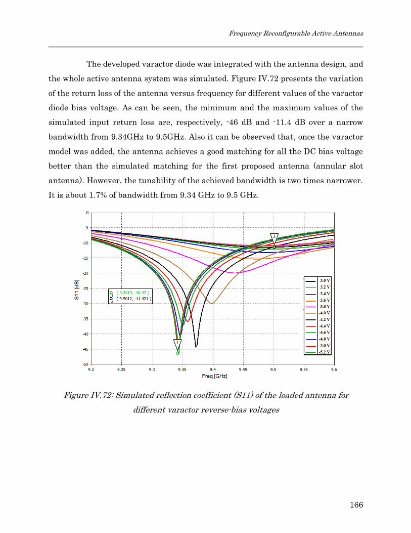
Frequency Reconfigurable Active Antennas
166
The developed varactor diode was integrated with the antenna design, and
the whole active antenna system was simulated. Figure IV.72 presents the variation
of the return loss of the antenna versus frequency for different values of the varactor
diode bias voltage. As can be seen, the minimum and the maximum values of the
simulated input return loss are, respectively, -46 dB and -11.4 dB over a narrow
bandwidth from 9.34GHz to 9.5GHz. Also it can be observed that, once the varactor
model was added, the antenna achieves a good matching for all the DC bias voltage
better than the simulated matching for the first proposed antenna (annular slot
antenna). However, the tunability of the achieved bandwidth is two times narrower.
It is about 1.7% of bandwidth from 9.34 GHz to 9.5 GHz.
Figure IV.72: Simulated reflection coefficient (S11) of the loaded antenna for
different varactor reverse-bias voltages

Realized GaN-Based Reconfigurable Circuits
167
3.3 Measured Return Loss and Radiation Pattern
To experimentally verify the simulated results of the antenna, the GaN
varactor was wire-bonded over the slot layer as depicted in Figure IV.67. The first
step is measure the return loss of the antenna at various DC bias value.
Unfortunately, when varying the DC bias nothing change on the input reflection
coefficient. We spent a lot of time to figure out where this problem comes, but we
could not understand. This can be due to misconnect of the varactor with the antenna
or/and the varactor device was broken during the wire-bonding steps. However, the
reflection coefficient, gain and radiation pattern have been measured at 0 V. As is
shown in Figure IV.73, the measured return loss of the antenna is around -7.3 dB at
10.6 GHz. Normally, at this bias point of 0 V, as was expected with simulation, the
return loss should be -11.4 dB at 9.5 GHz. There a shift of almost 1 GHz, this can be
due to the presence of the varactor even if it does not work as expected. The antenna
gain versus frequency at this bias point is displayed in Figure IV.74. A gain value of
5.6 dB is achieved at 10.6 GHz, while the simulated gain value for the antenna alone
at 11.35 GHz was around 7.1 dB. This gain difference can be due to the wires-bonding,
the SMA connector used for exciting the antenna, slightly higher dielectric losses of
the used substrates, and measurement uncertainty (e.g. a direction error) that were
not included in the simulation. The normalized radiation pattern in the E-plane and
H-plane at 10.6 GHz is depicted in Figure IV.75. In both planes, the antenna array
generates a cross-polarization level about -15 dB in the main lobe direction which is
two time larger to the simulated value. The simulated back side lobe in the main lobe
direction is about -10 dB which is closely corresponding to the simulated value (-12
dB). With the measurement of the radiation pattern, no side lobes are observed unlike
the simulation. This can be due to the presence in the E-plane of the connector that
excites the antenna. The simulation has been done without this connector.
It was a depth disappointment that the varactor cannot work as expected
to verify the simulation results. If so, this simple antenna structure would, no doubt,

Frequency Reconfigurable Active Antennas
168
have been a good application to validate our developed GaN varactor and also to
demonstrate the use of GaN device in reconfigurable antenna systems.
Figure IV.73: Measured return loss (S11) of the loaded antenna at no DC bias
applied
S11 [dB]
Freq [GHz]

Realized GaN-Based Reconfigurable Circuits
169
Figure IV.74 : Measured loaded antenna gain versus frequency at no bias DC
applied
Figure IV.75 : Measured normalized radiation pattern of the loaded antenna at 10.6
GHZ with no bias DC applied

Frequency Reconfigurable Active Antennas
170
4. Beam Steering Patch Antenna Arrays using GaN
SPDT Switch Structure
4.1 Antenna Design
In this section, an electronically beam steering antenna using the
developed SPDT switch structure is proposed for applications that operate at 2.45
GHz frequency. Again, the idea here is to validate the developed GaN SPDT switch
structure fabricated in NRC GaN500v2 process, for this a global system with four
rectangular 4x1 patch array antenna is designed to achieve a beam steering over the
H-plane for four Φ possibilities such as, 0°, 90°, 180° and 270°. With the use of this
structure, the global array antenna can steer its beam in H-plane by a single control
DC voltage (Vc_1, Vc_2, Vc_3 and Vc_4) applied at the different single switches
constituting the SPDT structure. In E-plane the beam is stable for all the SPDT
switch structures possibilities. As discussed in the section about SPDT switch
structure, the RF performances of this switch structure degrade versus frequency, so
at this frequency of 2.45 GHz, an isolation better than -25 dB and an insertion loss
around -3 dB have been predicted from the measurements of the single switches. In
addition, the antenna system was designed on Neltec substrate 9300 having Ԑr of 3.5
and a thickness t of 1.6 mm. Due to its high thickness, this substrate is very rigid and
make the vertical system easier to be mounted. Therefore a cooling plate was cut from
a piece of aluminium (Al), and is mounted on the backside (ground plane) of each 4x1
patch arrays antenna and of the feeding system design to transfers the heat
generated by GaN switch structure and provides an infrastructure to mount the
whole antenna system, the supply circuits and the RF connectors. The 3D model of
the designed antenna system is illustrated in Figure IV.76. The whole concept size is
14x14x29cm3. As shown in Figure IV.76, the four sides rectangular 4x1 patch array
antennas with series feed are placed perpendicular over the feeding system as
illustrated in Figure IV.77. Here 4 elements are used and each elements has the same

Realized GaN-Based Reconfigurable Circuits
171
dimensions with a length of 32 mm and a width of 38 mm in order to achieve higher
gain that can be still higher to 0 once the RF signal goes through all the losses due to
the SPDT (around -6 dB, wire-bonding and the substrate). In this design, the patch
elements are connected using microstrip line with a length around half-wavelength
(λg/2) in series feed and have been designed to operate around 2.45 GHz with input
impedance of 50 Ω. The length and the width of the each connecting microstrip line
are, respectively, 37.7 mm and 1 mm.
The SPDT switch structure are connected to the feeding system illustrated
in Figure IV.78 by using wires-bonding technique as zoomed and depicted in
Figure IV.79 while in Figure IV.80 a zoomed picture of the wires bonding is displayed
to show the connected pads of the SPDT switch. Moreover, to facilitate the wire
bonding connection between the feeding system design and the SPDT circuit, a gold
layer over the copper metal was added as seen in Figure IV.78.
Figure IV.76: 3D model of designed antenna system.

Frequency Reconfigurable Active Antennas
172
Figure IV.77: Fabricated
prototype of the antenna
Figure IV.78: The feeding system including the
three SPDT switch structures
Figure IV.79: Zoom on SPDT_1 switch
Figure IV.80: Zoom on the wires
bonding connecting the SPDT_1 to The
feeding system
SPDT_1
SPDT_2
SPDT_3 Port_2
Port_3
Port_4
Port_5
Vc_3
Vc_6 Vc_1
Vc_2
Vc_4 Vc_5
Port_1
GND RF_Input VC_4
VC_3
GND
GND
GND
RF_Output_1
RF_Output_2
GND

Realized GaN-Based Reconfigurable Circuits
173
For a better understanding of the antenna geometry, in Figure IV.77 the
fabricated final prototype is shown. One of the four 4x1 patch array antenna is
depicted in the Figure IV.81. The four 4x1 patch arrays antenna are fed by four
separated horizontal strips that are placed over a separated design using same Neltec
substrate (see Figure IV.78) along with the bias DC control network of the SPDT
switch structure. This design is called the feeding system. The four excitation strips
are joined together by matching circuit including the SPDT and the 4x1 patch
antenna array to 50 Ω. This matching circuit is based on quarter-wavelength (λg/4)
matching technique. It depends of the switching states of the SPDT ports, the
predicted impedances are summarized in Table IV.4. The coaxial probe is located at
joint point of all the four excitation strips, which acts as antenna feed.
Table IV.4: Predicted different impedances of the SPDT ports.
RF_Output_1 Port is ON and
RF_Output_2 Port is OFF
RF_Output_1 Port is OFF and
RF_Output_2 Port is ON
Impedance at RF_Input Port
75-j*20.6 (Ω) 75-j*20.6 (Ω)
Impedance at RF_Output_1 Port
77.05-j*18.6 (Ω) 60.10-j*9.85 (Ω)
Impedance at RF_Output_2 Port
60.10-j*9.85 (Ω) 77.05-j*18.6 (Ω)
As depicted in Figure IV.78, three SPDT switches were placed between the
four patch antenna arrays and the matching circuit. The first one was placed to steer
the beam for 0° and 90°, the second one to scan the beam for 180° and 270°, while the
third one was placed between the main feeding transmission line (connected to the
cable coaxial) and the two first SPDT to switch the RF signal to a one of them at once.
Due to unavailability of a complete model of the SPDT switch structure, as mentioned
in Chapter III in SPDT switch section, depending upon the state of the SPDT switch
a short circuit or open circuit was used between the corresponding patch antenna
array and the matching circuit when necessary to conduct the EM simulation.
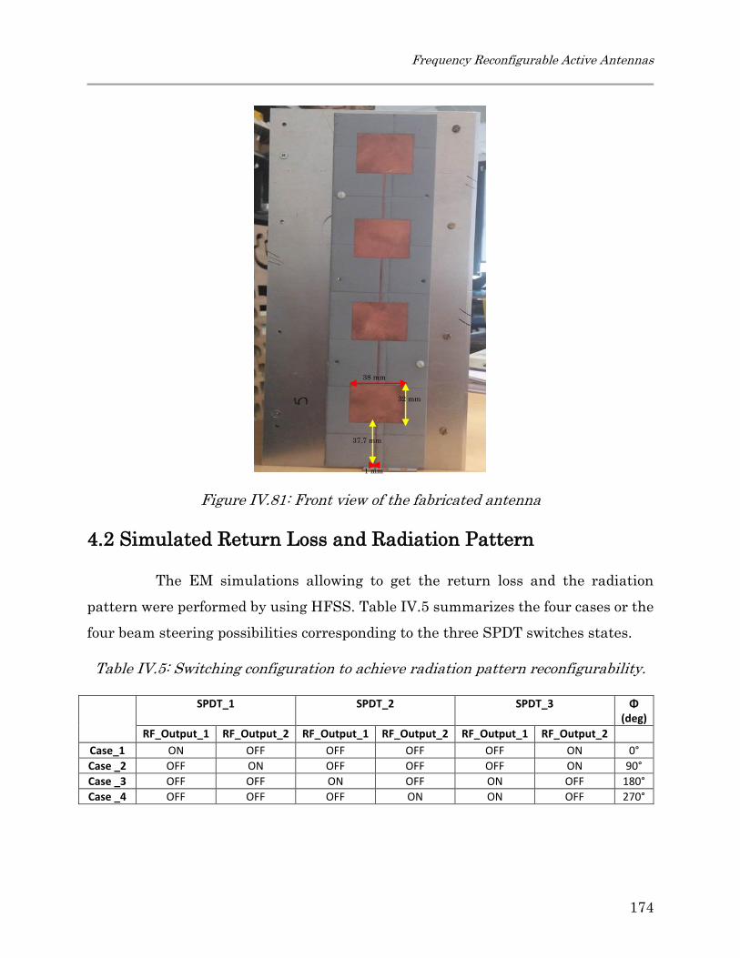
Frequency Reconfigurable Active Antennas
174
Figure IV.81: Front view of the fabricated antenna
4.2 Simulated Return Loss and Radiation Pattern
The EM simulations allowing to get the return loss and the radiation
pattern were performed by using HFSS. Table IV.5 summarizes the four cases or the
four beam steering possibilities corresponding to the three SPDT switches states.
Table IV.5: Switching configuration to achieve radiation pattern reconfigurability.
SPDT_1 SPDT_2 SPDT_3 Φ (deg)
RF_Output_1 RF_Output_2 RF_Output_1 RF_Output_2 RF_Output_1 RF_Output_2
Case_1 ON OFF OFF OFF OFF ON 0°
Case _2 OFF ON OFF OFF OFF ON 90°
Case _3 OFF OFF ON OFF ON OFF 180°
Case _4 OFF OFF OFF ON ON OFF 270°
38 mm
32 mm
37.7 mm
1 mm

Realized GaN-Based Reconfigurable Circuits
175
As highlighted in one 4x1 patch arrays antenna return loss which is shown
in Figure IV.82, an impedance bandwidth of approximately 40 MHz (2.45 GHz to 2.41
GHz) is achieved, with a resonance frequency sensing at approximately 2.43 GHz. At
this frequency, a return loss value better than -30 dB is obtained in simulation for
one 4x1 patch arrays antenna. Because the return loss of the four 4x1 patch arrays
antenna are similar, here we report only return loss for one which corresponding to
one case.
The radiation pattern in H-plane corresponding to the four cases
possibilities is shown in Figure IV.84. A shift of 90° between the four cases in the
radiation pattern is clearly achieved. The 3-dB beam width where the four beam
configuration cases intersect for each case is found to be approximately 85°.
For a better understanding of beam switching, the antenna radiation
pattern is tilted towards the positive z-axis having maximum at Φ=90°, θ=0°, here
switches are configured as mentioned in Table IV.5 for case 1, is tilled towards the
positive x-axis when switches are configured as mentioned in case 2 having maximum
at Φ= 0°, θ=90°, is tilled towards the negative z-axis when switches are configured as
mentioned in case 3 having maximum at Φ= 90°, θ=-180° and for the fourth case it is
tilled towards the negative x-axis when switches are configured as mentioned in case
4 having maximum at Φ= -180°, θ=-90°.
The overall gain of one 4x1 patch arrays antenna is found to be above 10.9
dB at the operating frequency of 2.43 as depicted in Figure IV.83. It is important to
keep in mind that in the EM simulation only short and open were used instead of the
model of the SPDT, this means that almost -3dB of losses of one SPDT switch
structure has to be considered. So this will results on the maximum antenna gain
value that would decrease with almost -6 dB because the RF signal go through two
SPDT switch structures as explained in Table IV.5 . Furthermore, there will be also
other losses due to the substrate and the wires-bonding connecting the SPDT to the

Frequency Reconfigurable Active Antennas
176
transmission lines. The overall losses is measured for every case and will be
presented later in this section.
Figure IV.82: Simulated return loss of the antenna
Figure IV.83: Simulated antenna gain versus frequency

Realized GaN-Based Reconfigurable Circuits
177
Figure IV.84: Simulated normalized H-plane at 2.43 GHz for four cases mentioned
in Table IV.4
Figure IV.85: Simulated normalized E-plane at 2.43 GHz
Case 1
Case 2
Case 3
Case 4
Frequency Reconfigurable Active Antennas
178
4.3 Measured Return Loss and Radiation Pattern
Here, the experimentally measurements are presented and results are
discussed. These measurements will verify the simulation results. Figure IV.86
shows the return loss of one fabricated 4x1 patch arrays antenna prototype. It
indicates that the 4x1 patch arrays antenna presents a good match with |S11| of -
25.5 dB at a resonant frequency of 2.43 GHz which is completely corresponding to
what was achieved with simulation where a |S11| of -28.6 dB was obtained at 2.43
GHz. This value of the return loss was verified for all four fabricated 4x1 patch arrays
antenna, and here we report only return loss for one which corresponding to one
case. The antenna gain versus frequency is displayed in Figure IV.87. A gain value
of 10.1 dB is achieved at 2.43 GHz, while the simulated gain value for the antenna
alone at this frequency was around 10.9 dB. Conductor losses, slightly higher
dielectric losses of the used substrate, also some set up errors during the
measurement, can be the main reasons of the 0.8 dB gain difference. As was expected,
this measured gain of 10.1 dB decreased by almost -7 dB once the measurement with
the SPDT structure is conducted. -6 dB corresponding to the losses of the two SPDT
structures as explained in Chapter III in Figure III.57 while the -1 dB is due to the
substrate losses, the transmission lines and the wire banding.
The simulated radiation pattern of the patch array antenna in both H-
plane and E-plane has been verified by measurement at 2.43 GHz. Satisfactory
agreement with the simulation was achieved as shown in Figure IV.88 where the
measured radiation pattern in the H-plane for four cases is illustrated while in
Figure IV.89 depicts the measured radiation pattern in the E-plane. It is seen that
the beam steering operation of the radiation pattern in H-plane is achieved over the
expected four direction. The radiation pattern shows the cross-pol level in the
broadside direction lower than –30 dB in the H-plane and –25 dB in the E-plane and
a low side lobes of –15 dB in the E-plane.

Realized GaN-Based Reconfigurable Circuits
179
Figure IV.86: Measured return loss of the antenna
Figure IV.87: Measured antenna gain versus frequency

Frequency Reconfigurable Active Antennas
180
Figure IV.88: Measured normalized H plane at 2.43 GHz for four cases mentioned
in Table IV.4
Figure IV.89: Measured normalized E plane at 2.43 GHz

Realized GaN-Based Reconfigurable Circuits
181
4.4 Measured Insertion Loss and Isolation of the Feeding
System
4.4.1 Small Signal Measurements
Depending on the two states of the three SPDT switch structures (as
indicated in Table IV.5), the s-parameters at the different four ports, Port_1, Port_2,
Port_3, Port_4 and Port_5, (see Figure IV.78) of the feeding system design have been
measured. The s-parameters measurements are to be made between the common
port, Port_1, and one of the others output ports, either Port_1, Port_2, Port_3 or
Port_4.
When the SPDT is configured for case_1, the insertion loss is measured
between the Port_1 and the Port_2 along with the isolation at the other ports. As
illustrated in Figure IV.90, the insertion loss and the isolation are shown. It can be
seen that the return loss at both ports (i.e Port_1 and Port_2) indicates low reflections
around -6.8 dB at the frequency of interest 2.43 GHz since at this frequency the input
port and the two output ports of the three SPDT have well matched to 50 Ω. Because
the RF signal go from Port_1 to Port_2 through two SPDT switch, the measured -6.8
dB insertion loss value is due to the insertion loss of SPDT switches which was around
-3 dB as would be expected for one SPDT and the losses of the used substrate, the
metal and the wires bond which can be -0.8 dB. The measured isolation is higher than
-25 dB at all ports and all configurations cases.
Similarly, the same considerations of measurement are applied if the
measurements are between the Port_1 and the other output ports. In Figure IV.91,
Figure IV.92 and Figure IV.93, the measured insertion loss and the isolation are
displayed, respectively, for case_2, case_3 and case_4. It is clearly seen that,
depending the case, measured the insertion loss is around -7.14 dB (i.e case_2) at the
worst value and is around -6.62 dB (i.e case_4) at the good value. This difference of

Frequency Reconfigurable Active Antennas
182
0.5 dB can be due mainly to the misconnection (i.e weld the connector) of the SMA
connector at the different ports.
Figure IV.90: Measured S-parameters for case_1 at Pin of 0 dBm
Figure IV.91: Measured S-parameters for case_2 at Pin of 0 dBm
Realized GaN-Based Reconfigurable Circuits
183
Figure IV.92: Measured S-parameters for case_3 at Pin of 0 dBm
Figure IV.93: Measured S-parameters for case_4 at Pin of 0 dBm

Frequency Reconfigurable Active Antennas
184
4.4.2 Large Signal Measurements
The objective here is to demonstrate that GaN-based switch structure can
simultaneously achieve reasonably high power handling capability without
sacrificing insertion loss and isolation. To satisfy these requirements, a RF power
sweep from 0 dBm to 30 dBm at the Port_1 has been done and the insertion losses
were measured between Port_1 and Port_2 at these different level of power.
The measured power handling capability of the SPDT switch at 2.43 GHz
is shown in Figure IV.94. The insertion loss for ON state was measured with the
increasing of input power level at 2.43 GHz for case_1 configuration. As seen the
insertion loss remains almost constant up to 16 dBm input power. The measured data
shown in Figure IV.94 demonstrates less than 1 dB of compression for 20 dBm
incident RF power at 2.43 GHz. The input power capability of 20 dBm handled by the
used GaN transistor can be confirm the potential of using GaN technology for high
power regarding the small size of these used devices (as mentioned in Switch
modeling section, the devices used are 2x25 µm and 2x50 µm gate width).
Figure IV.94: Measured insertion loss versus input RF power for case_1 at 2.43 GHz

Realized GaN-Based Reconfigurable Circuits
185
VI. Summary
This preceding chapter deals with implementing reconfigurable designs to
validate and verify the use of our developed GaN varactors and switches and
demonstrate the feasibility of using GaN technology in tunable RF/microwaves
systems. Reconfigurable designs such as phase shifter, 3-dB 90° hybrid coupler,
oscillator and patch antenna arrays were designed and discussed. The
reconfigurablity operation is achieved by using the developed GaN HEMT-based
varactor and switch devices as was expected. These GaN circuits were embedded with
the listed design by using the wire bonding technique.

Summary
186
Chapter V
---------------------------------------------------------------------------------------------------------------------
Conclusion and Future Work
This thesis is primarily focused on developing models of varactor diodes
and switches fabricated using the newest semiconductor technology, gallium nitride
(GaN). Varactor and switch devices play a crucial role in design, development and
overall performance of wireless communication systems that require
reconfigurablity. The thesis can be divided into two major parts: modeling of GaN-
based devices such as varactor diodes and switches, and reconfigurable designs where
these developed GaN devices are integrated.
The active devices structure studied here are based on GaN HEMT
processes offered by National Research Council. Three GaN processes, such as,
GaN150v0 with a gate length of 0.15 um, GaN500v1 with gate length of 0.5 um and
GaN500v2, have been used for manufacturing the varactor diodes and the switches.
Based on these three GaN processes, many varactors have been fabricated and
characterized. A general small signal and large signal model based on analytic

Conclusion and Future Work
187
equations containing empirical coefficients have been introduced for the first time for
the voltage dependency of equivalent capacitance (CEq) and series resistance (REq).
For small signal model, all of the developed analytic equations, which describe REq
and CEq versus the control DC voltage (VG), are only bias voltage and device geometry
dependent, while for large signal, the influence of RF power has been taken into
account in the proposed analytic expressions describing the behaviour of REq and CEq.
These proposed analytical solutions agree remarkably well with the experimentally
extracted C-V curves for several RF power and can be used as a general model to
represent the nonlinear behavior of GaN based varactor devices. By analyzing the C-
V curve, we conclude that the equivalent series capacitance is dependent on the
geometry of fingers. This means that the larger is the device, the higher are the
capacitance values. Moreover, it was observed that the extracted capacitance values
from varactors with GaN500v2 are at least twice as large as those extracted with the
same device size fabricated with GaN500v1 process. The tuning range of the varactor
diode is limited, and it was found that over a range of 1 V, the CEq changes rapidly.
In addition, an equivalent simple physical circuit model was proposed and simulated,
yielding good agreement between the simulated and the measured results. The
obtained Cmax/Cmin ratios and figures of merit compare favorably with recently
reported GaN varactors.
On the other hand, different size single standalone switches and switch
structures such as single pole single throw (SPST) and single pole double throw
(SPDT) were fabricated using NRC GaN500v2 and were presented. Here only small
signal measurement were presented and discussed. It was observed that, with a
single transistor in common gate configuration, the isolation is good at low
frequencies but quickly drops with increasing frequency. In addition, it was observed
that the more the device is large, the lower the insertion loss achieved but the poorer
the isolation will be. A trade-off between insertion loss and isolation has been made
to choose the single transistors that will be used for designing switch structures such
as SPST and SPDT which could improve the performances at high frequencies.

Summary
188
Comparing to the standalone device, it was revealed that with SPST structure, the
isolation is improved while the insertion loss slightly dropped by -1 dB. With this
proposed topology, it is still a challenge to meet good performance at our higher
frequency. Another topology based on SPDT was proposed to improve more the
performances. As was expected with this topology, some improvement in isolation is
achieved compared to SPST, while the insertion loss is increased by almost -1 dB. For
example, at 2.45 GHz (frequency of interest) isolation better than -25 dB and an
insertion loss of -3 dB were achieved. However, the SPDT structure performances
degrade with frequency. Moreover, based on these small signal measurements, a
model was introduced. In addition, the fabricated SPDT switch structure will be
integrated with antenna system to demonstrate the ability of using GaN devices for
a beam switching antenna array.
Finally, in this thesis, the use of GaN on highly efficient reconfigurable
designs for broadband RF/microwave applications operating below 10 GHz was
demonstrated. The varactors and switches used for tunable purpose were firstly
fabricated, characterized and then modeled. The proposed models were used to
achieve the reconfigurability of RF/microwave circuits. Tunable phase shifter,
reconfigurable 3-dB 90° hybrid coupler, tunable frequency oscillator, beam switching
antenna array and matching reconfigurable patch antenna were developed along
with the development of GaN modeling varactors and switches, and were presented
as applications results of this thesis research.
Using GaN150v0 process, two reconfigurable RF designs have been
designed and reported. Firstly, a GaN phase shifter design based on reflective
topology has been described, and only simulation results were presented. First, the
3-dB 90° hybrid coupler has been designed and simulated using NRC GaN150 PDK.
Then two developed GaN varactors were placed on the two coupler’s output ports as
loads. Under different bias conditions varying from -3.5 V to -5.5 V, the return loss of
the phase shifter is better than 20 dB across a 1 GHz bandwidth centered at 10 GHz,

Conclusion and Future Work
189
while good match is achievable over this range of 9.5–10.5 GHz. Worst case of the
insertion loss is about -3 dB at 10 GHz and occurs at a bias point of -4.3 V where the
equivalent resistor of the used varactors is significantly high. Therefore, a
continuously variable phase-shift range of 80° is achieved at 10 GHz. Secondly, a
varactor tunable broadband quadrature hybrid coupler has been investigated and
simulated from X-band to Ku-band frequencies applications, and only simulated
results were reported. First, a static coupler has been designed to meet the
specifications of a typical quadrature hybrid coupler (3-dB insertion loss, good return
and isolation loss, and 90° phase difference between coupled and through ports) at 10
GHz. Then, a tunable broadband coupler has been designed by inserting varactor
diodes as shunt capacitance elements in order to control the operating frequency. This
design occupies an area of 1.35×0.9 mm2 and good simulation results have been
demonstrated. This novel varactor reconfigurable hybrid coupler is proposed to
overcome the need of high power tunable RF/microwave circuits which are required
for multi-standard and multiservice applications. By changing the bias voltage of the
varactor to control the resonance condition of parallel LC resonator, this proposed
hybrid coupler can provide the desired operating frequency from 10 GHz to 16 GHz.
Over this bandwidth, the overall return loss is better than -13.5 dB over a tuning
range 1 V while the isolation is below than -14 dB. In addition, the simulated
magnitude of S21 parameter is close to -3.5 dB and is getting poorer as varactor
capacitance values decreases. A worst value of -5 dB is achieved at the minimum
capacitance value. While at port 3, the S31 parameter behaves as S21 but in a reverse
way. As a result, the amplitude imbalance is varying from -0.2 dB at 10 GHz and -2
dB at 16 GHz. A minimum well-balanced quadrature phase of 86° is obtained between
the coupled port 2 and the through port 3. This phase is increasing and getting closer
to 92 ° as varactor capacitor values are decreasing.
Using GaN500v2 process, a tunable frequency GaN oscillator was designed
by loading symmetrically the feedback loop, and was presented. For tuning purpose,
the previous developed GaN varactors were used. The oscillation frequency values

Summary
190
change significantly and a minimum oscillation frequency of 7.8 GHz was achieved
when CEq is at its maximum for VG above -3.5 V, and a maximum oscillation frequency
of 8.6 GHz was simulated when CEq is at its minimum for VG bellow -4.5 V. While,
when VG varies from -5 V to -3.7 V, the oscillation frequency values change
significantly and a tuning bandwidth of 0.8 GHz is obtained, corresponding to a
tuning range about 10%. The output power is about 20.5 dBm and almost stable over
all bias levels with a slight variation over range (2) when VG varies while a good phase
noise value of -112 dBc/Hz is met at 100 KHz. Also three reconfigurable antennas
were designed and presented. The first design is a simple element square loop
coplanar antenna printed onto glass substrate. The frequency tunability has been
achieved by loading the previous developed GaN varactor diode. The antenna was
electronically tuned by varying the varactor bias voltage applied at the gate, VG. As
reposted, the minimum and the maximum values of the measured input return loss
are, respectively, -6.9 dB and -7.1 dB over the bandwidth from 7.53GHz to 7.85GHz
corresponding to a tunability up to 4% narrow bandwidth inside. This frequency
tunability is achieved by using a developed GaN varactor. Another frequency
reconfigurability antenna was described and presented. The used structure is based
on aperture coupled microstrip patch antenna feed technique. The antenna structure
with overall dimensions L of 50 mm and W of 50 mm consists of two dielectric layers:
a slot layer and a simple element patch layer and between them an air-gap layer of
1mm. As presented, the minimum and the maximum values of the simulated input
return loss are, respectively, -48 dB and -13 dB over a narrow bandwidth from
9.34GHz to 9.5GHz. This tunability is achieved by integrating a developed varactor
with the antenna design. The last reported reconfigurable antenna design is an
electronically beam steering antenna using the developed SPDT switch structure is
proposed for applications that operate at 2.45 GHz frequency. The idea here is to
verify the developed GaN SPDT switch structure fabricated in NRC GaN500v2
process, for this a global system with four patch arrays antenna with beam steering
over the H plane for four Φ possibilities such as, 0°, 90°, 180° and 270° is designed.

Conclusion and Future Work
191
With the use of this structure, the global array can steer its beam by a single control
DC voltage applied at the different single switches constituting the SPDT structure.
Some contributions to the field of microwave integrated and reconfigurable
circuit designs have been made from this thesis research. As mentioned in Chapter
III, one journal paper [149] has been published and one other has been submitted
[151]. A conference paper has also been presented at the European Microwave
Conference in Paris in 2015 [150]. Furthermore, a part of the work of the beam
steering patch antenna arrays using GaN SPDT switch that was presented in
Chapter IV section 4 will be presented at the European Conference on Antennas and
Propagation in Paris in 2017
[152] and also based on the antenna work one journal paper is expecting to
be submitted for publication.
Despite all the obstacles that we faced during the manufacturing of the
GaN design (such as, runs cancelled, chips dicing …), we succeed to overcome some
of them and develop GaN varactor and switch devices which were later integrated
with PCB designs to achieve reconfigurability.
There are several areas related to this thesis which are ripe for study. First,
if the required equipment became available, large-signal GaN device modeling,
particularly for varactor switch devices is an area which should be developed.
Improved performance in large signal operation and going higher in frequency of
these devices can be expected when improved commercial NRC GaN150 become fully
available.
Initially, a NRC GaN150 run was planned and highly miniaturized phase
shifter and reconfigurable hybrid coupler designs were planned to be fabricated and
tested. Unfortunately these designs have not been manufactured because the run has
been cancelled by NRC. So future work could be include both phase shifter and
reconfigurable hybrid coupler using the advanced developed version of NRC GaN150

Summary
192
process. Also it was expected to develop a frequency tunable antenna feeder such as
annular slot antenna using varactor diode for reconfigurability. This feeder can be
used to tune the frequency of an antenna that is fabricated by using a low cost
substrate.

Bibliography
1
Bibliography
[1] D. W. Runton, B. Trabert, J. B. Shealy, and R. Vetury, “History of GaN: High-
Power RF Gallium Nitride (GaN) from Infancy to Manufacturable Process and
Beyond,” IEEE Microwave Magazine, vol. 14, no. 3, pp. 82–93, imsspecialissuemay
2013.
[2] T. Ross, G. Cormier, and K. Hettak, “Gallium nitride hybrid microwave circuits
for low-noise applications,” in 2010 14th International Symposium on Antenna Technology and Applied Electromagnetics the American Electromagnetics Conference (ANTEM-AMEREM), 2010, pp. 1–4.
[3] U. Johannsen, M. I. Kazim, A. B. Smolders, and M. H. A. J. Herben, "Modular
antenna array concept for millimeter-wave beam-steering applications," Progress in Electromagnetics Research Symposium Proceedings, Stockholm, Sweden, Aug.
12-15, 2013.
[4] K. Joshin, T. Kikkawa, S. Masuda and K. Watanabe, “Outlook for GaN HEMT
technology”, Fujitsu Sci. Tech. J.50, 138-143. 2014.
[5] N. J. Kolias, “Recent advances in Ga N MMIC technology,” in 2015 IEEE Custom Integrated Circuits Conference (CICC), 2015, pp. 1–5.
[6] G. Callet, " Caractérisation et Modélisation de Transistors HEMT AlGaN/GaN
et InAlN/GaN pour l’Amplification de puissance en Radio-Fréquences," PhD Dissertation. University of Limoges. 2011.
[7] W. Saito, Y. Takada, M. Kuraguchi, K. Tsuda, I. Omura, and T. Ogura, “600V
AlGaN/GaN power-HEMT: design, fabrication and demonstration on high voltage
DC-DC converter,” in Electron Devices Meeting, 2003. IEDM ’03 Technical Digest. IEEE International, 2003, p. 23.7.1-23.7.4.
[8] J. Delaine, P. O. Jeannin, D. Frey, and K. Guepratte, “High frequency DC-DC
converter using GaN device,” in 2012 Twenty-Seventh Annual IEEE Applied Power Electronics Conference and Exposition (APEC), 2012, pp. 1754–1761.
[9] A. Brown, K. Brown, J. Chen, K. C. Hwang, N. Kolias, and R. Scott, “W-band
GaN power amplifier MMICs,” in Microwave Symposium Digest (MTT), 2011 IEEE MTT-S International, 2011, pp. 1–4.
[10] Y. Nakasha, S. Masuda, K. Makiyama, T. Ohki, M. Kanamura, N. Okamoto, T.
Tajima, T. Seino, H. Shigematsu, K. Imanishi, T. Kikkawa, K. Joshin, and N. Hara,
“E-Band 85-mW Oscillator and 1.3-W Amplifier ICs Using 0.12 #181;m GaN
HEMTs for Millimeter-Wave Transceivers,” in 2010 IEEE Compound Semiconductor Integrated Circuit Symposium (CSICS), 2010, pp. 1–4.
[11] M. Micovic, A. Kurdoghlian, K. Shinohara, I. Milosavljevic, S. D. Burnham, M.
Hu, A. L. Corrion, W. S. Wong, A. Schmitz, P. B. Hashimoto, P. J. Willadsen, D. H.
Chow, A. Fung, R. H. Lin, L. Samoska, P. P. Kangaslahti, B. H. Lambrigtsen, and
P. F. Goldsmith, “W-band GaN MMIC with 842 mW output power at 88 GHz,” in
Microwave Symposium Digest (MTT), 2010 IEEE MTT-S International, 2010, pp.
1–1.

Bibliography
2
[12] J. W. Milligan, S. Sheppard, W. Pribble, Y. F. Wu, G. Muller, and J. W.
Palmour, “SiC and GaN Wide Bandgap Device Technology Overview,” in 2007 IEEE Radar Conference, 2007, pp. 960–964.
[13] W. Saito, Y. Takada, M. Kuraguchi, K. Tsuda, I. Omura, T. Ogura, and H.
Ohashi, “High breakdown voltage AlGaN-GaN power-HEMT design and high
current density switching behavior,” IEEE Transactions on Electron Devices, vol.
50, no. 12, pp. 2528–2531, Dec. 2003.
[14] T. Zimmermann, D. Deen, Y. Cao, J. Simon, P. Fay, D. Jena, and H. G. Xing,
“AlN/GaN Insulated-Gate HEMTs With 2.3 A/mm Output Current and 480 mS/mm
Transconductance,” IEEE Electron Device Letters, vol. 29, no. 7, pp. 661–664, Jul.
2008.
[15] Y. f Wu, M. Moore, A. Saxler, T. Wisleder, and P. Parikh, “40-W/mm Double
Field-plated GaN HEMTs,” in 2006 64th Device Research Conference, 2006, pp.
151–152.
[16] Discrete GaAs pHEMT, TGF2018, Rev. D, TriQuint Semiconductor, Nov. 2013.
[17] Discrete power GaN on SiC HEMT, TGF2023-2-01, Rev. C, TriQuint
Semiconductor, Sep. 2013.
[18] Q. Rüdiger, “Gallium Nitride Electronics,” vol. 96. Berlin, Heidelberg: Springer Berlin Heidelberg, 2008.
[19] Md. Tanvir Hasan “Mechanism and Suppression of Current Collapse in
AlGaN/GaN High Electron Mobility Transistors”. PhD Dissertation. University of
Fukui, Fukui, Japan, 2013.
[20] R. Vetury, N. Q. Zhang, S. Keller, and U. K. Mishra, “The impact of surface
states on the DC and RF characteristics of AlGaN/GaN HFETs,” IEEE Transactions on Electron Devices, vol. 48, no. 3, pp. 560–566, Mar. 2001.
[21] O. Mitrofanov and M. Manfra, “Mechanisms of gate lag in GaN/AlGaN/GaN
high electron mobility transistors,” Superlattices and Microstructures, vol. 34, no.
1–2, pp. 33–53, Jul. 2003.
[22] P. B. Klein and S. C. Binari, "Photoionization spectroscopy of deep defects
responsible for current collapse in nitride-based field effect transistors," Journal of Physics: Condensed Matter, 15 (2003) R1641–R1667. PII: S0953-8984(03)58996-2
[23] M. Faqir, G. Verzellesi, A. Chini, F. Fantini, F. Danesin, G. Meneghesso, E.
Zanoni, and C. Dua, “Mechanisms of RF Current Collapse in AlGaN #x2013;GaN
High Electron Mobility Transistors,” IEEE Transactions on Device and Materials Reliability, vol. 8, no. 2, pp. 240–247, Jun. 2008.
[24] S. Nakamura, M. Senoh, S. Nagahama, N. Iwasa, T. Yamada, T. Matsushita,
H. Kiyoku, Y. Sugimoto, T. Kozaki, H. Umemoto, M. Sano, and K. Chocho,
“Continuous-wave operation of InGaN/GaN/AlGaN based laser diodes grown on
GaN substrates”, Applied Physics. Letters, vol. 72, no. 16, Apr. 1998, pp. 2014–2016.
[25] T. Paskova, D. A. Hanser, and K. R. Evans, “GaN Substrates for III-Nitride
Devices,” Proceedings of the IEEE, vol. 98, no. 7, pp. 1324–1338, Jul. 2010.

Bibliography
3
[26] Hageman, P.R.; Kirilyuk, V.; Corbeek, W.H.M.; Weyher, J.L.; Lucznik, B.;
Bockowski, M.; Porowski, S.; Müller, S. “Thick GaN layers grown by hydride vapor-
phase epitaxy: hetero- versus homo-epitaxy”. Journal of Crystal Growth 255 (2003),
No.3-4, pp.241-249.
[27] R. Dwilinski, R. Doradzinski, J. Garczynski, L. P. Sierzputowski, A. Puchalski,
Y. Kanbara, K. Yagi, H. Minakuchi, and H. Hayashi, “Bulk ammonothermal GaN”,
Journal of Crystal Growth, vol. 311, no. 10, May 2009, pp. 3015–3018.
[28] T. Hashimoto, E. Letts, M. Ikari, and Y. Nojima, “Improvement of crystal
quality in ammonothermal growth of bulk GaN”, Journal of Crystal Growth, vol.
312, no. 18, Sep. 2010, pp. 2503–2506.
[29] B. Łucznik, B. Pastuszka, I. Grzegory, M. Bockowski, G. Kamler, E. Litwin-
Staszewska, and S. Porowski, “Deposition of thick GaN layers by HVPE on the
pressure grown GaN substrates”, Journal of Crystal Growth, vol. 281, no. 1, Jul.
2005, pp. 38–46.
[30] T. N. Ross. “Gallium Nitride Phase Shifters”. PhD Dissertation. March, 2015.
Carleton University, Ottawa, Canada.
[31] “Gallium Nitride MMIC Foundry Design Manual GaN500v2,” Canadian Photonics Fabrication Center. National Research Council Canada, 2013.
[32] H. Tang, J. B. Webb, and J. A. Bardwell. “The ammonia- MBE approach for
high electron mobility in GaN epilayers and AlGaN/GaN HFET structures”.
[33] J. Bardwell, T. Lester, H. Tang, B. Surridge, A. Harrison, and A. Lau,
“AlGaN/GaN Transistors and Circuits,” ECS Trans., vol. 16, no. 7, pp. 193–198, Oct.
2008.
[34] T. Edwards, “Semiconductor Technology Trends for Phased Array Antenna
Power Amplifiers,” in 2006 European Radar Conference, 2006, pp. 269–272.
[35] T. Ohira, Y. Suzuki, H. Ogawa, and K. Kamitsuna, “Megalithic microwave
signal processing for phased-array beamforming and steering,” IEEE Transactions on Microwave Theory and Techniques, vol. 45, no. 12, pp. 2324–2332, Dec. 1997.
[36] L. F. Eastman and U. K. Mishra, “The toughest transistor yet [GaN
transistors],” IEEE Spectrum, vol. 39, no. 5, pp. 28–33, May 2002.
[37] B. Heying, W. Luo, I. Smorchkova, S. Din, and M. Wojtowicz, “Reliable GaN
HEMTS for high frequency applications,” in Microwave Symposium Digest (MTT), 2010 IEEE MTT-S International, 2010, pp. 1–1.
[38] M. Oppermann, F. Thurow, and B. Bunz, “GaN/SiC MMICs and packaging for
use in future transmit / receive modules,” in Electronics System-Integration Technology Conference (ESTC), 2014, 2014, pp. 1–4.
[39] C. Lin, H. Liu, and Y. Zheng, “Application of GaN high power chips in T/R
modules,” in 2013 Proceedings of the International Symposium on Antennas Propagation (ISAP), 2013, vol. 1, pp. 515–518.
Bibliography
4
[40] N. J. Kolias and M. T. Borkowski, “The development of T/R modules for radar
applications,” in Microwave Symposium Digest (MTT), 2012 IEEE MTT-S International, 2012, pp. 1–3.
[41] H. Yukawa, M. Hangai, H. Mizutani, K. Yamanaka, M. Abe, A. Inoue, and M.
Miyazaki, “Q-band gaas MMIC modules for active phased array antenna systems,”
in Microwave Conference, 2009. EuMC 2009. European, 2009, pp. 464–467.
[42] D. Baccello, M. D’Antoni, B. Orobello, and E. Sperduti, “Miniaturised low cost
solid state 4W TXRX common leg for 6 #x00F7;18 GHz phased array,” in Microwave Symposium Digest (MTT), 2010 IEEE MTT-S International, 2010, pp. 401–403.
[43] P. Schuh, H. Sledzik, R. Reber, A. Fleckenstein, R. Leberer, M. Oppermann, R.
Quay, F. van Raay, M. Seelmann-Eggebert, R. Kiefer, and M. Mikulla, “GaN MMIC
based T/R-Module Front-End for X-Band Applications,” in Microwave Integrated Circuit Conference, 2008. EuMIC 2008. European, 2008, pp. 274–277.
[44] S. Masuda, M. Yamada, T. Ohki, K. Makiyama, N. Okamoto, Y. Nakasha, K.
Imanishi, T. Kikkawa, and H. Shigematsu, “C-Ku band GaN MMIC T/R frontend
module using multilayer ceramics technology,” in Microwave Symposium Digest (MTT), 2011 IEEE MTT-S International, 2011, pp. 1–4.
[45] D. Gustafsson, J. C. Cahuana, D. Kuylenstierna, I. Angelov, and C. Fager, “A
GaN MMIC Modified Doherty PA With Large Bandwidth and Reconfigurable
Efficiency,” IEEE Transactions on Microwave Theory and Techniques, vol. 62, no.
12, pp. 3006–3016, Dec. 2014.
[46] V. Jantarachote, N. Sirivech, and S. Chalermwisutkul, “Frequency band and
operating class reconfigurable GaN HEMT power amplifier for sustainable wireless
communications and energy applications,” in The 20th Asia-Pacific Conference on Communication (APCC2014), 2014, pp. 156–160.
[47] O. L. Chlieh, W. T. Khan, and J. Papapolymerou, “Microfluidically
reconfigurable GaN power amplifier on multilayer organic substrate for s-band and
c-band applications,” in 2015 IEEE MTT-S International Microwave Symposium,
2015, pp. 1–4.
[48] R. Pengelly, S. Sheppard, T. Smith, B. Pribble, S. Wood and C. Platis,
“Commercial GaN Devices for Switching and Low Noise Applications”, CS MANTECH Conference, Palm Springs, CA, USA, May 2011.
[49] X. Lan, M. Wojtowicz, M. Truong, F. Fong, M. Kintis, B. Heying, I. Smorchkova,
and Y. C. Chen, “A V-Band Monolithic AlGaN/GaN VCO,” IEEE Microwave and Wireless Components Letters, vol. 18, no. 6, pp. 407–409, Jun. 2008.
[50] T. N. Ross, G. Cormier, K. Hettak, and J. S. Wight, “High-power X-band GaN
switched-filter phase shifter,” in 2014 IEEE MTT-S International Microwave Symposium (IMS2014), 2014, pp. 1–4.
[51] K. Andersson, V. Desmaris, J. Eriksson, N. Rorsman, and H. Zirath, “C-band
linear resistive wide bandgap FET mixers,” in Microwave Symposium Digest, 2003 IEEE MTT-S International, 2003, vol. 2, pp. 1303–1306 vol.2.

Bibliography
5
[52] C. Jin, E. Okada, M. Faucher, D. Ducatteau, M. Zaknoune, and D. Pavlidis, “A
GaN Schottky Diode-based analog phase shifter MMIC,” in European Microwave Integrated Circuit Conference (EuMIC), 2014 9th, 2014, pp. 96–99.
[53] M. Marso, J. Bernat, A. Wolter, P. Javorka, A. Fox, and P. Kordos, “MSM diodes
based on an AlGaN/GaN HEMT layer structure for varactor and photodiode
application,” in The Fourth International Conference on Advanced Semiconductor Devices and Microsystems, 2002, 2002, pp. 295–298.
[54] C. S. Chu, Y. Zhou, K. J. Chen, and K. M. Lau, “Q-factor characterization of RF
GaN-based metal-semiconductor-metal planar interdigitated varactor,” IEEE Electron Device Letters, vol. 26, no. 7, pp. 432–434, Jul. 2005.
[55] L. B. Chang, S. C. Wang, S. L. Lin, M. Das, Y. C. Ferng, M. J. Cheng, S. T.
Chou, and L. Chow, “Fast surge suppression by inserting an AlGaN/GaN-based
varactor,” in 2012 2nd International Conference on Consumer Electronics, Communications and Networks (CECNet), 2012, pp. 3251–3253.
[56] C.-Y. Tien; P.-Y. Kuei ; Liann-Be Chang ; C.-P. Hsu. "Capacitance Swing and
Capacitance Ratio of GaN-Based Metal-Semiconductor-Metal Two-Dimensional
Electron Gas Varactor with Different Dielectric Films", Journal of Electrical Engineering and Technology 10(4):1721-1726. July 2015.
[57] C. Jin, D. Pavlidis, and L. Considine, “A novel GaN-based high frequency
varactor diode,” in Microwave Integrated Circuits Conference (EuMIC), 2010 European, 2010, pp. 118–121.
[58] W. Lu, L. Wang, S. Gu, D. P. R. Aplin, D. M. Estrada, P. K. L. Yu, and P. M.
Asbeck, “InGaN/GaN Schottky Diodes With Enhanced Voltage Handling Capability
for Varactor Applications,” IEEE Electron Device Letters, vol. 31, no. 10, pp. 1119–
1121, Oct. 2010.
[59] W. Lu, L. Wang, S. Gu, P. M. Asbeck, and P. K. L. Yu, “Critical design
considerations for GaN-based microwave power varactors,” in 2012 IEEE International Conference on Electron Devices and Solid State Circuit (EDSSC), 2012, pp. 1–4.
[60] S.Arulkumaran, T. Egawa, H. Ishikawa, T. Jimbo, and Y. Sano, "Surface
passivation effects on AlGaN/GaN high-electron-mobility transistors with SiO2,
Si3N4, and silicon oxynitride," Appl. Phys. Lett., vol. 84, pp. 613-615, 2004.
[61] J. S. Lee, J. W. Kim, J. H. Lee, C. S. Kim, J. E. Oh, M. W. Shin, and J. H. Lee,
“Reduction of current collapse in AlGaN/GaN HFETs using AlN interfacial layer,”
Electronics Letters, vol. 39, no. 9, pp. 750–752, May 2003.
[62] Y. F. Wu, A. Saxler, M. Moore, R. P. Smith, S. Sheppard, P. M. Chavarkar, T.
Wisleder, U. K. Mishra, and P. Parikh, “30-W/mm GaN HEMTs by field plate
optimization,” IEEE Electron Device Letters, vol. 25, no. 3, pp. 117–119, Mar. 2004.
[63] A. P. Edwards, J. A. Mittereder, S. C. Binari, D. S. Katzer, D. F. Storm, and J.
A. Roussos, “Improved reliability of AlGaN-GaN HEMTs using an NH3 plasma
treatment prior to SiN passivation,” IEEE Electron Device Letters, vol. 26, no. 4,
pp. 225–227, Apr. 2005.

Bibliography
6
[64] N. Miura, T. Nanjo, M. Suita, T. Oishi, Y. Abe, T. Ozeki, H. Ishikawa, T. Egawa,
and T. Jimbo, “Thermal annealing effects on Ni/Au based Schottky contacts on n-
GaN and AlGaN/GaN with insertion of high work function metal,” Solid-State Electronics, vol. 48, no. 5, pp. 689–695, May 2004.
[65] Y. Takei, M. Kamiya, K. Tsutsui, W. Saito, K. Kakushima, H. Wakabayashi, Y.
Kataoka, and H. Iwai, “Reduction of contact resistance on AlGaN/GaN HEMT
structures introducing uneven AlGaN layers,” Phys. Status Solidi A, vol. 212, no. 5,
pp. 1104–1109, May 2015.
[66] M. Okamoto, K. Kakushima, Y. Kataoka, A. Nishiyama, N. Sugii, H.
Wakabayashi, K. Tsutsui, H. Iwai, and W. Saito, “An ohmic contact process for
AlGaN/GaN structures using TiSi2 electrodes,” in 2013 IEEE Workshop on Wide Bandgap Power Devices and Applications (WiPDA), 2013, pp. 159–161.
[67] W. Saito, I. Omura, T. Ogura, and H. Ohashi, “Theoretical limit estimation of
lateral wide band-gap semiconductor power-switching device,” Solid-State Electronics, vol. 48, no. 9, pp. 1555–1562, Sep. 2004.
[68] S. Lucyszyn, G. Green, and I. D. Robertson, “Accurate millimeter-wave large
signal modeling of planar Schottky varactor diodes,” in Microwave Symposium Digest, 1992., IEEE MTT-S International, 1992, pp. 259–262 vol.1.
[69] W. Ciccognani, M. Ferrari, and E. Limiti, “High isolation microstrip GaN-
HEMT Single-FET Switch,” Int J RF and Microwave Comp Aid Eng, vol. 20, no. 4,
pp. 391–398, Jul. 2010.
[70] A. Bettidi, A. Cetronio, W. Ciccognani, M. De Dominicis, C. Lanzieri, E. Limiti,
A. Manna, M. Peroni, C. Proietti, and P. Romanini, “High power GaN-HEMT SPDT
switches for microwave applications,” Int J RF and Microwave Comp Aid Eng, vol.
19, no. 5, pp. 598–606, Sep. 2009.
[71] L. Devlin, “The design of integrated switches and phase shifters,” in Design of RFICs and MMICs (Ref. No. 1999/158), IEE Tutorial Colloquium, 1999, p. 2/1-2/14.
[72] N. Q. Zhang, B. Moran, S. P. DenBaars, U. K. Mishra, X. W. Wang, and T. P.
Ma, “Effects of surface traps on breakdown voltage and switching speed of GaN
power switching HEMTs,” in Electron Devices Meeting, 2001. IEDM ’01. Technical Digest. International, 2001, p. 25.5.1-25.5.4.
[73] H. Ishida, Y. Hirose, T. Murata, A. Kanda, Y. Ikeda, T. Matsuno, K. Inoue, Y.
Uemoto, T. Tanaka, T. Egawa, and D. Ueda, “A high power Tx/Rx switch IC using
AlGaN/GaN HFETs,” in Electron Devices Meeting, 2003. IEDM ’03 Technical Digest. IEEE International, 2003, p. 23.6.1-23.6.4.
[74] H. Ishida, Y. Hirose, T. Murata, Y. Ikeda, T. Matsuno, K. Inoue, Y. Uemoto, T.
Tanaka, T. Egawa, and D. Ueda, “A high-power RF switch IC using AlGaN/GaN
HFETs with single-stage configuration,” IEEE Transactions on Electron Devices,
vol. 52, no. 8, pp. 1893–1899, Aug. 2005.
[75] V. Kaper, R. Thompson, T. Prunty and J. R. Shealy, “Monolithic AlGaN/GaN
HEMT SPDT switch,” 12th GAAS Symposium. Amsterdam, 2004.

Bibliography
7
[76] U. K. Mishra, P. Parikh, and Y.-F. Wu, “AlGaN/GaN HEMTs-an overview of
device operation and applications,” Proceedings of the IEEE, vol. 90, no. 6, pp. 1022–
1031, Jun. 2002.
[77] B. Y. Ma, K. S. Boutros, J. B. Hacker, and G. Nagy, “High power AlGaN/GaN
Ku-band MMIC SPDT switch and design consideration,” in Microwave Symposium Digest, 2008 IEEE MTT-S International, 2008, pp. 1473–1476.
[78] J. Janssen, K. P. Hilton, J. O. Maclean, D. J. Wallis, J. Powell, M. Uren, T.
Martin, M. van Heijningen, and F. van Vliet, “X-Band GaN SPDT MMIC with over
25 Watt Linear Power Handling,” in Microwave Integrated Circuit Conference, 2008. EuMIC 2008. European, 2008, pp. 190–193.
[79] K. Hettak, T. Ross, N. Irfan, D. Gratton, M. C. E. Yagoub, and J. Wight, “High-
power broadband GaN HEMT SPST/SPDT switches based on resonance inductors
and shunt-stacked transistors,” in Microwave Integrated Circuits Conference (EuMIC), 2012 7th European, 2012, pp. 215–218.
[80] X. Zheng, J. C. Tremblay, S. E. Huettner, K. P. Ip, T. Papale, and K. L. Lange,
“Ka-Band High Power GaN SPDT Switch MMIC,” in 2013 IEEE Compound Semiconductor Integrated Circuit Symposium (CSICS), 2013, pp. 1–5.
[81] I. Angelov, H. Zirath, and N. Rosman, “A new empirical nonlinear model for
HEMT and MESFET devices,” IEEE Transactions on Microwave Theory and Techniques, vol. 40, no. 12, pp. 2258–2266, Dec. 1992.
[82] I. Angelov, N. Rorsman, J. Stenarson, M. Garcia, and H. Zirath, “An empirical
table-based FET model,” IEEE Transactions on Microwave Theory and Techniques,
vol. 47, no. 12, pp. 2350–2357, Dec. 1999.
[83] W. R. Curtice, “Nonlinear modeling of compound semiconductor HEMTs, state
of the art,” in Microwave Symposium Digest (MTT), 2010 IEEE MTT-S International, 2010, pp. 1–1.
[84] S. C. Binari, K. Ikossi, J. A. Roussos, W. Kruppa, D. Park, H. B. Dietrich, D. D.
Koleske, A. E. Wickenden, and R. L. Henry, “Trapping effects and microwave power
performance in AlGaN/GaN HEMTs,” IEEE Transactions on Electron Devices, vol.
48, no. 3, pp. 465–471, Mar. 2001.
[85] O. Jardel, F. D. Groote, T. Reveyrand, J. C. Jacquet, C. Charbonniaud, J. P.
Teyssier, D. Floriot, and R. Quere, “An Electrothermal Model for AlGaN/GaN Power
HEMTs Including Trapping Effects to Improve Large-Signal Simulation Results on
High VSWR,” IEEE Transactions on Microwave Theory and Techniques, vol. 55, no.
12, pp. 2660–2669, Dec. 2007.
[86] F. Lin and G. Kompa, “FET model parameter extraction based on optimization
with multiplane data-fitting and bidirectional search-a new concept,” IEEE Transactions on Microwave Theory and Techniques, vol. 42, no. 7, pp. 1114–1121,
Jul. 1994.
[87] C. van Niekerk and P. Meyer, “Performance and limitations of decomposition-
based parameter extraction procedures for FET small-signal models,” IEEE Transactions on Microwave Theory and Techniques, vol. 46, no. 11, pp. 1620–1627,
Nov. 1998.

Bibliography
8
[88] I. Angelov, L. Bengtsson, and M. Garcia, “Extensions of the Chalmers nonlinear
HEMT and MESFET model,” IEEE Transactions on Microwave Theory and Techniques, vol. 44, no. 10, pp. 1664–1674, Oct. 1996.
[89] L. Dunleavy, C. Baylis, W. Curtice, and R. Connick, “Modeling GaN: Powerful
but Challenging,” IEEE Microwave Magazine, vol. 11, no. 6, pp. 82–96, Oct. 2010.
[90] T. N. Ross, K. Hettak, G. Cormier, and J. S. Wight, “Design of X-Band GaN
Phase Shifters,” IEEE Transactions on Microwave Theory and Techniques, vol. 63,
no. 1, pp. 244–255, Jan. 2015.
[91] J. A. Pla and W. Struble, “Nonlinear model for predicting intermodulation
distortion in GaAs FET RF switch devices,” in Microwave Symposium Digest, 1993., IEEE MTT-S International, 1993, pp. 641–644 vol.2.
[92] G. Boeck, D. Plenkowski, R. Circa, M. Otte, B. Heyne, P. Rykaczewski, R.
Wittmann, and R. Kakerow, “RF front-end technology for reconfigurable mobile
systems,” in Microwave and Optoelectronics Conference, 2003. IMOC 2003. Proceedings of the 2003 SBMO/IEEE MTT-S International, 2003, vol. 2, pp. 863–
868 vol.2.
[93] V. Vidojkovic, J. van der Tang, A. Leeuwenburgh, A. van Roermund, "Adaptive
Multi-Standard RF Front-Ends," Springer Netherlands, 2008, pp. 1–16.
[94] F. Eshghabadi, F. Banitorfia, N. M. Noh, A. A. Manaf, M. T. Mustaffa, and O.
Sidek, “MEMS-based Reconfigurable CMOS LNAs for Wireless Applications,”
Trends in Applied Sciences Research, vol. 7, no. 4, pp. 273–284, Apr. 2012.
[95] E. Lourandakis, R. Weigel, H. Mextorf, and R. Knoechel, “Circuit Agility,”
IEEE Microwave Magazine, vol. 13, no. 1, pp. 111–121, Jan. 2012.
[96] J. MANUEL, “Composants innovants reconfigurables par voie optique pour des
applications microondes,” PhD Dissertation. University of Limoges. 2011.
[97] G. B. Norris, D. C. Boire, G. S. Onge, C. Wutke, C. Barratt, W. Coughlin, and
J. Chickanosky, “A fully monolithic 4-18 GHz digital vector modulator,” in
Microwave Symposium Digest, 1990., IEEE MTT-S International, 1990, pp. 789–
792 vol.2.
[98] R. V. Garver, “Broad-Band Diode Phase Shifters,” IEEE Transactions on Microwave Theory and Techniques, vol. 20, no. 5, pp. 314–323, May 1972.
[99] K. Hettak, T. Ross, D. Gratton, and J. Wight, “A new type of GaN HEMT based
high power high-pass/low-pass phase shifter at X band,” in Microwave Symposium Digest (MTT), 2012 IEEE MTT-S International, 2012, pp. 1–3.
[100] T. N. Ross, G. Cormier, K. Hettak, and J. S. Wight, “High-power X-band GaN
switched-filter phase shifter,” in 2014 IEEE MTT-S International Microwave Symposium (IMS2014), 2014, pp. 1–4.
[101] C. Jin, E. Okada, M. Faucher, D. Ducatteau, M. Zaknoune, and D. Pavlidis,
“A GaN Schottky Diode-based analog phase shifter MMIC,” in European Microwave Integrated Circuit Conference (EuMIC), 2014 9th, 2014, pp. 96–99.

Bibliography
9
[102] R. V. Garver, “360° Varactor Linear Phase Modulator,” IEEE Transactions on Microwave Theory and Techniques, vol. 17, no. 3, pp. 137–147, Mar. 1969.
[103] H. A. Atwater, “Reflection Coefficient Transformations for Phase-Shift
Circuits,” IEEE Transactions on Microwave Theory and Techniques, vol. 28, no. 6,
pp. 563–568, Jun. 1980.
[104] R. C. Frye, S. Kapur, and R. C. Melville, “A 2-GHz quadrature hybrid
implemented in CMOS technology,” IEEE Journal of Solid-State Circuits, vol. 38,
no. 3, pp. 550–555, Mar. 2003.
[105] "Gallium Nitride MMIC Foundry Design Manual GaN150," Canadian Photonics Fabrication Center. National Research Council Canada, 2015
[106] R. C. Waterman, W. Fabian, R. A. Pucel, Y. Tajima, and J. L. Vorhaus, “GaAs
monolithic Lange and Wilkinson couplers,” IEEE Transactions on Electron Devices,
vol. 28, no. 2, pp. 212–216, Feb. 1981.
[107] S. Lucyszyn and I. D. Robertson, “Analog reflection topology building blocks
for adaptive microwave signal processing applications,” IEEE Transactions on Microwave Theory and Techniques, vol. 43, no. 3, pp. 601–611, Mar. 1995.
[108] C.-L. Chen, W. E. Courtney, L. J. Mahoney, M. J. Manfra, A. Chu, and H. A.
Atwater, “A Low-Loss Ku-Band Monolithic Analog Phase Shifter,” IEEE Transactions on Microwave Theory and Techniques, vol. 35, no. 3, pp. 315–320,
Mar. 1987.
[109] F. Ellinger, R. Vogt, and W. Bachtold, “Compact reflective-type phase-shifter
MMIC for C-band using a lumped-element coupler,” IEEE Transactions on Microwave Theory and Techniques, vol. 49, no. 5, pp. 913–917, May 2001.
[110] H. Hayashi, T. Nakagawa, and K. Araki, “A miniaturized MMIC analog phase
shifter using two quarter-wave-length transmission lines,” IEEE Transactions on Microwave Theory and Techniques, vol. 50, no. 1, pp. 150–154, Jan. 2002.
[111] R. Scheeler and Z. Popović, “GaAs MMIC tunable directional coupler,” in
Microwave Symposium Digest (MTT), 2012 IEEE MTT-S International, 2012, pp.
1–3.
[112] B. Hur and W. R. Eisenstadt, “Tunable Broadband MMIC Active Directional
Coupler,” IEEE Transactions on Microwave Theory and Techniques, vol. 61, no. 1,
pp. 168–176, Jan. 2013.
[113] R. V. Gatti, A. Ocera, S. Bastioli, L. Marcaccioli, and R. Sorrentino, “A Novel
Compact Dual Band Reconfigurable Power Divider for Smart Antenna Systems,” in
2007 IEEE/MTT-S International Microwave Symposium, 2007, pp. 423–426.
[114] S. Voinigescu, “High-Frequency Integrated Circuits”, Cambridge University Press, 2013.
[115] A. Balandin, S. V. Morozov, S. Cai, R. Li, K. L. Wang, G. Wijeratne, and C. R.
Viswanathan, “Low flicker-noise GaN/AlGaN heterostructure field-effect
transistors for microwave communications,” IEEE Transactions on Microwave Theory and Techniques, vol. 47, no. 8, pp. 1413–1417, Aug. 1999.

Bibliography
10
[116] S. Shin, G. Choi, H. Kim, S. Lee, S. Kim, and J. Choi, “Frequency-tunable
high-efficiency power oscillator using GaN HEMT,” in Microwave Symposium Digest (MTT), 2010 IEEE MTT-S International, 2010, pp. 1–1.
[117] M. Hörberg, L. Szhau, T. N. T. Do, and D. Kuylenstierna, “Phase noise
analysis of a tuned-input/tuned-output oscillator based on a GaN HEMT device,” in
Microwave Conference (EuMC), 2014 44th European, 2014, pp. 1118–1121.
[118] H. Mostardinha, P. M. Cabral, N. B. Carvalho, P. Kurpas, M. Rudolph, J.
Würfl, J. C. Pinto, A. Barnes, and F. Garat, “GaN RF oscillator used in space
applications,” in 2010 Workshop on Integrated Nonlinear Microwave and Millimeter-Wave Circuits (INMMIC), 2010, pp. 50–53.
[119] S. Kim, H. Kim, S. Shin, J. Kim, B. Kim, and J. Choi, “Combined power
oscillator using GaN HEMT,” in Microwave Symposium Digest (MTT), 2011 IEEE MTT-S International, 2011, pp. 1–1.
[120] C. Bansleben and W. Heinrich, “Compact high-power GaN oscillator with 2.45
GHz differential output,” in Microwave Conference (EuMC), 2013 European, 2013,
pp. 818–821.
[121] J. B. Shealy, J. A. Smart, and J. R. Shealy, “Low-phase noise AlGaN/GaN
FET-based voltage controlled oscillators (VCOs),” IEEE Microwave and Wireless Components Letters, vol. 11, no. 6, pp. 244–245, Jun. 2001.
[122] H. Xu, C. Sanabria, N. K. Pervez, S. Keller, U. K. Mishra, and R. A. York,
“Low phase-noise 5 GHz AlGaN/GaN HEMT oscillator integrated with BaxSr1-
xTiO3 thin films,” in Microwave Symposium Digest, 2004 IEEE MTT-S International, 2004, vol. 3, p. 1509–1512 Vol.3.
[123] C. Sanabria, H. Xu, S. Heikman, U. K. Mishra, and R. A. York, “A GaN
differential oscillator with improved harmonic performance,” IEEE Microwave and Wireless Components Letters, vol. 15, no. 7, pp. 463–465, Jul. 2005.
[124] C. Kong, H. Li, X. Chen, S. Jiang, J. Zhou, and C. Chen, “A Monolithic
AlGaN/GaN HEMT VCO Using BST Thin-Film Varactor,” IEEE Transactions on Microwave Theory and Techniques, vol. 60, no. 11, pp. 3413–3419, Nov. 2012.
[125] H. Liu, X. Zhu, C. C. Boon, X. Yi, M. Mao, and W. Yang, “Design of Ultra-Low
Phase Noise and High Power Integrated Oscillator in GaN-on-SiC HEMT
Technology,” IEEE Microwave and Wireless Components Letters, vol. 24, no. 2, pp.
120–122, Feb. 2014.
[126] H. Xu, C. Sanabria, S. Heikman, S. Keller, U. K. Mishra, and R. A. York, “High
power GaN oscillators using field-plated HEMT structure,” in IEEE MTT-S International Microwave Symposium Digest, 2005., 2005, p. 4 pp.-pp.
[127] H. Kao, B.-W. Wang, C.-S. Yeh, C.-L. Cho, B.-H. Wei, and H.-C. Chiu, “High
Power and Low Phase Noise MMIC VCO Using 0.35m GaN-on-Si HEMT,”
International Journal of Computer Theory and Engineering, pp. 910–913, 2013.
[128] T. N. T. Do, S. Lai, M. Horberg, H. Zirath, and D. Kuylenstierna, “A MMIC
GaN HEMT Voltage-Controlled-Oscillator with High Tuning Linearity and Low

Bibliography
11
Phase Noise,” in 2015 IEEE Compound Semiconductor Integrated Circuit Symposium (CSICS), 2015, pp. 1–4.
[129] K. V, V. Tilak, H. Kim, R. Thompson, T. Prunty, J. Smart, L. F. Eastman, and
J. R. Shealy, “High power monolithic AlGaN/GaN HEMT oscillator,” in Gallium Arsenide Integrated Circuit (GaAs IC) Symposium, 2002. 24th Annual Technical Digest, 2002, pp. 251–254.
[130] Z. Q. Cheng, Y. Cai, J. Liu, Y. Zhou, K. M. Lau, and K. J. Chen, “A Low Phase-
Noise -Band MMIC VCO Using High-Linearity and Low-Noise Composite-Channel
HEMTs,” IEEE Transactions on Microwave Theory and Techniques, vol. 55, no. 1,
pp. 23–29, Jan. 2007.
[131] G. Soubercaze-Pun, J. G. Tartarin, L. Bary, J. Rayssac, E. Morvan, B.
Grimbert, S. L. Delage, J. c D. Jaeger, and J. Graffeuil, “Design of a X-band GaN
oscillator: from the low frequency noise device characterization and large signal
modeling to circuit design,” in 2006 IEEE MTT-S International Microwave Symposium Digest, 2006, pp. 747–750.
[132] S. Lai, D. Kuylenstierna, M. Özen, M. Hörberg, N. Rorsman, I. Angelov, and
H. Zirath, “Low Phase Noise GaN HEMT Oscillators With Excellent Figures of
Merit,” IEEE Microwave and Wireless Components Letters, vol. 24, no. 6, pp. 412–
414, Jun. 2014.
[133] M. Hörberg and D. Kuylenstierna, “Low phase noise power-efficient MMIC
GaN-HEMT oscillator at 15 GHz based on a quasi-lumped on-chip resonator,” in
2015 IEEE MTT-S International Microwave Symposium, 2015, pp. 1–4.
[134] M. Hörberg, T. Emanuelsson, S. Lai, T. N. D. Thanh, H. Zirath, and D.
Kuylenstierna, “Phase-Noise Analysis of an X-Band Ultra-Low Phase-Noise GaN
HEMT Based Cavity Oscillator,” IEEE Transactions on Microwave Theory and Techniques, vol. 63, no. 8, pp. 2619–2629, Aug. 2015.
[135] X. Lan, M. Wojtowicz, I. Smorchkova, R. Coffie, R. Tsai, B. Heying, M. Truong,
F. Fong, M. Kintis, C. Namba, A. Oki, and T. Wong, “A Q-band low phase noise
monolithic AlGaN/GaN HEMT VCO,” IEEE Microwave and Wireless Components Letters, vol. 16, no. 7, pp. 425–427, Jul. 2006.
[136] X. Lan, M. Wojtowicz, M. Truong, F. Fong, M. Kintis, B. Heying, I.
Smorchkova, and Y. C. Chen, “A V-Band Monolithic AlGaN/GaN VCO,” IEEE Microwave and Wireless Components Letters, vol. 18, no. 6, pp. 407–409, Jun. 2008.
[137] J. B. Shealy, T. Jackson, A. Rachlin, M. Poulton, N. Bukhari, K. Ditzler, X.
Gong, L. Sumpter, and D. Weeks, “A 2 watt Ku-band linear (multi-carrier) transmit
module for VSAT applications,” in Microwave Symposium Digest, 1999 IEEE MTT-S International, 1999, vol. 3, pp. 1055–1058 vol.3.
[138] H. Zirath, R. Kozhuharov, and M. Ferndahl, “Balanced Colpitt oscillator
MMICs designed for ultra-low phase noise,” IEEE Journal of Solid-State Circuits,
vol. 40, no. 10, pp. 2077–2086, Oct. 2005.

Bibliography
12
[139] Cree’s CGHV1J025D datasheet.
[140] M. Caillet, “Etude et Conception d’un Système Radar Courte Portée et
d’Antennes Reconfigurables en Bande Millimétrique,” PhD Dissertation.
University of Rennes 1, Rennes, France. November, 2006.
[141] S. Sufyar, C. Delaveaud, and R. Staraj, “A frequency agility technique on a
miniature omnidirectional antenna,” in Proceedings of the Fourth European Conference on Antennas and Propagation, 2010, pp. 1–4.
[142] S. K. Dhar, O. Hammi, M. S. Sharawi, and F. M. Ghannouchi, “Power
amplifier based integrated and miniaturized active antenna,” in 2015 9th European Conference on Antennas and Propagation (EuCAP), 2015, pp. 1–4.
[143] V. K. Varadan, K. A. Jose, and V. V. Varadan, “Design and development of
electronically tunable microstrip antennas,” Smart Mater. Struct., vol. 8, no. 2, p.
238, 1999.
[144] R. B. Whatley, Z. Zhou, and K. L. Melde, “Reconfigurable RF impedance tuner
for match control in broadband wireless devices,” IEEE Transactions on Antennas and Propagation, vol. 54, no. 2, pp. 470–478, Feb. 2006.
[145] A. Hamdoun, L. Roy, M. Himdi, and O. Lafond, “Characterization of GaN-
based HEMTs as varactor diode devices,” in Microwave Integrated Circuits Conference (EuMIC), 2015 10th European, 2015, pp. 417–420.
[146] "An Update on New Tunable Technologies", From July 2010 High Frequency Electronics. Copyright © 2010 Summit Technical Media, LLC.
[147] A. Martin, X. Castel, O. Lafond, and M. Himdi, “Optically transparent
frequency-agile antenna for X-band applications,” Electronics Letters, vol. 51, no.
16, pp. 1231–1233, 2015.
[148] J. S. McLean, “A re-examination of the fundamental limits on the radiation Q
of electrically small antennas,” IEEE Transactions on Antennas and Propagation,
vol. 44, no. 5, p. 672-, May 1996.
[149] A. Hamdoun, L. Roy, M. Himdi, and O. Lafond, “Characterisation and
analytical modelling of GaN HEMT-based varactor diodes,” Electronics Letters, vol.
51, no. 23, pp. 1930–1932, 2015.
[150] A. Hamdoun, L. Roy, M. Himdi, and O. Lafond, “Characterization of GaN-
based HEMTs as varactor diode devices,” in Microwave Integrated Circuits Conference (EuMIC), 2015 10th European, 2015, pp. 417–420.
[151] A. Hamdoun, L. Roy, M. Himdi and O. Lafond, "Large Signal Analytic
Modeling of HEMT-based Varactor Diodes," Submitted to IEEE Transactions on
Electron Devices IEEE. September 2016.
[152] A. Hamdoun, L. Roy, M. Himdi and O. Lafond, "Switched Beam Patch Array
Antenna Using SPDT GaN HEMT Switches," in European Conference on Antennas and Propagatione (EuCAP), 11th European, Paris 2015.