Embed Size (px)
Citation preview
Abstract—In modern VLSI technology the speed and power
would always be a trade off. In contrast to that the proposed
design gives better technique in improving the speed of
computation with high accuracy when compared with
conventional adders. And also the implementation gives low
power results with better performance. Using the available
VLSI design techniques and emerging concepts the high speed
low power high accurate (HS-LP-HA) Adder is proposed. The
proposed HS-LP-HA adder is capable to give near accurate
value along with much low power consumption when compared
with conventional adder. Hence also improved power delay
product. The proposed HS-LP-HA adder finds its applications
in signal processing for communications, control of systems,
biomedical signal processing and seismic data processing in all
which the minute percentage of error is tolerable.
Index Terms—HS-LP-HA adder, speed, low power, accuracy,
signal processing, percentage of error.
I. INTRODUCTION
Now a day‟s technology designs are looking for minimized
circuit techniques through which to increase the throughput
of the system. The system throughput may be increased by
optimal logic minimization in data path elements for error
tolerant applications. Examples for such circuits are full
adders. It is found that not all full adders used to construct
the data path elements such as ripple carry adders and array
multipliers. The probability of an input combination
occurring at a node is generally either (a) only dependent on
the input test vectors at a node (b) only dependent on current
topology (c) a combination of both [1]. Logic minimization
not only results in better system throughput but also results in
low power consumption designs. For low power results it is
always advisable to use CMOS technology in which the
power dissipation is a complex function of the gate delays,
clock frequency, process parameters, circuit topology and
structure, and the input vectors applied. Once the processing
and structural parameters have been fixed, the measure of
power dissipation is dominated by the switching activity
(toggle count) of the circuit .The dynamic power is given by,
P=1/2 × Cload × (Vdd2/Tcycle) × E(switching),
where Cload is the load capacitance of the gate, Tcycle is the
clock cycle time, E(switching) is the expected number of
Manuscript received March 17, 2013; revised May 19, 2013.
Muddapu Parvathi is with the Electronics and Communication Engineering Department in Malla Reddy Institute of Technology and
Science, Secunderabad, Andhra Pradesh, India, (e-mail: bendalamieee@
gmail.com). N. Vasantha is with Information Technology Department in Vasavi
College of Engineering, Andhra Pradesh, India.
K. Satya Prasad is with the Electronics and Communication Engineering
Department, JNTUK, Kakinada, Andhra Pradesh, India.
signal transitions per cycle and Vdd is the supply voltage [2],
[3]. Though Some error tolerant circuits such as ETAI and
ETAII [4]-[7] are designed but are suffered from accuracy
problem when small number inputs are considered. And also
as they were implemented with conventional adder design
which results in high power dissipation such limitations are
eliminated in the design of HS-LP-HA adder.
The rest of the paper is organized as follows. Section II
includes the addition arithmetic as well as the structure of the
HS-LP-HA adder. In Section III, The experimental results
and comparisons between conventional adder and
HS-LP-HA adder are shown. Section IV provides
conclusions.
II. ADDITION ARITHMETIC IN HS-LP-HA ADDER
The HS-LP-HA Adder strictly follows error calculation
mechanism for its accuracy measurement. Given the
dominance of applications with varying output significance,
the metric used is Relative Error Magnitude for qualifying the
error in the in exact circuits, used widely in [8]-[12],
computed as
Relative Error Magnitude =
1
|1 k k
k k
O O
O
where ν is the total number of simulation cycles or test
vectors given to the circuit, kO is the expected correct output
vector andkO is the obtained erroneous output vector for the
kth input vector [10].
Accuracy by definition is the measure of how close a
measurement is to the true value and is given by ( 1- relative
error magnitude)×100% and Its value ranges from 0% to
100%.
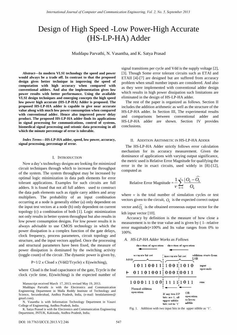
A. HS-LP-HA Adder Works as Follows
Fig. 1. Addition with two input bits in the upper nibble as „1‟.
Design of High Speed -Low Power-High Accurate
(HS-LP-HA) Adder
Muddapu Parvathi, N. Vasantha, and K. Satya Prasad
International Journal of Computer and Communication Engineering, Vol. 2, No. 5, September 2013
547DOI: 10.7763/IJCCE.2013.V2.246
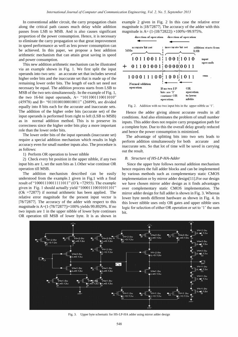
In conventional adder circuit, the carry propagation chain
along the critical path causes much delay while addition
passes from LSB to MSB. And is also causes significant
proportion of the power consumption. Hence, it is necessary
to eliminate the carry propagation so that great improvement
in speed performance as well as less power consumption can
be achieved. In this paper, we propose a best addition
arithmetic mechanism that can attain great saving in speed
and power consumption.
This new addition arithmetic mechanism can be illustrated
via an example shown in Fig. 1. We first split the input
operands into two sets: an accurate set that includes several
higher order bits and the inaccurate set that is made up of the
remaining lower order bits. The length of each set need not
necessary be equal. The addition process starts from LSB to
MSB of the two sets simultaneously. In the example of Fig. 1,
the two 16-bit input operands, A= “1011001110011010”
(45978) and B= “0110100100010011” (26899), are divided
equally into 8 bits each for the accurate and inaccurate sets.
The addition of the higher order bits (accurate set) of the
input operands is performed from right to left (LSB to MSB)
as in normal addition method. This is to preserve its
correctness since the higher order bits play a more important
role than the lower order bits.
The lower order bits of the input operands (inaccurate set)
require a special addition mechanism which results in high
accuracy even for small number inputs also. The procedure is
as follows:
1) Perform OR operation to lower nibble
2) Check every bit position in the upper nibble, if any two
input bits are 1, set the sum bits as 1.Other wise continue OR
operation till MSB.
The addition mechanism described can be easily
understood from the example.1 given in Fig.1 with a final
result of “10001110011111011” (Oˆk =72955). The example
given in Fig. 1 should actually yield “10001110010101101”
(Ok =72877) if normal arithmetic has been applied. The
relative error magnitude for the present input vector is
|78/72877|. The accuracy of the adder with respect to this
magnitude is A=(1-|78/72877|)×100% yields 99.8929%. If no
two inputs are 1 in the upper nibble of lower byte continues
OR operation till MSB of lower byte. It is as shown in
example 2 given in Fig. 2 In this case the relative error
magnitude is |18/72877|. The accuracy of the adder with this
magnitude is A= (1-|18/72822|) ×100%=99.975%.
Fig. 2. Addition with no two input bits in the upper nibble as „1‟.
Hence the adder giving almost accurate results in all
conditions. And also eliminates the problem of small number
inputs. This adder does not require carry propagation path for
a complete byte. Due to this the overall delay greatly reduced
and hence the power consumption is minimized.
The advantage of splitting bits into two sets leads to
perform addition simultaneously for both accurate and
inaccurate sets. So that lot of time will be saved in carrying
out the result.
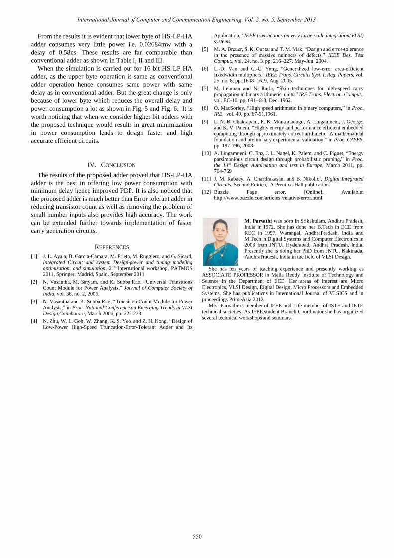
B. Structure of HS-LP-HA-Adder
Since the upper byte follows normal addition mechanism
hence requires the full adder blocks and can be implemented
by various methods such as complementary static CMOS
implementation or by mirror adder design[11].For our design
we have chosen mirror adder design as it finds advantages
over complementary static CMOS implementation. The
mirror adder design for full adder is shown in Fig. 3. Whereas
lower byte needs different hardware as shown in Fig. 4. In
this lower nibble uses only OR gates and upper nibble uses
logic for selection of either OR operation or set to „1‟ the sum
bit.
Fig. 3. Upper byte schematic for HS-LP-HA adder using mirror adder design
International Journal of Computer and Communication Engineering, Vol. 2, No. 5, September 2013
548
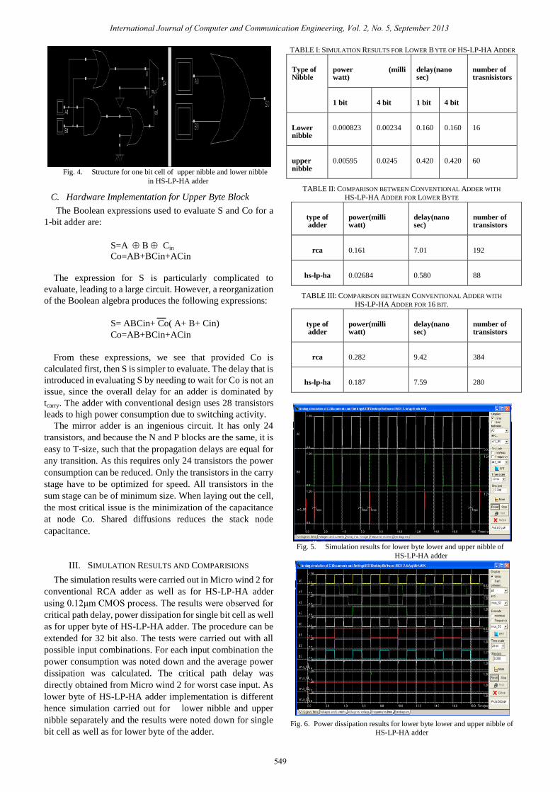
Fig. 4. Structure for one bit cell of upper nibble and lower nibble
in HS-LP-HA adder
C. Hardware Implementation for Upper Byte Block
The Boolean expressions used to evaluate S and Co for a
1-bit adder are:
S=ACin
Co=AB+BCin+ACin
The expression for S is particularly complicated to
evaluate, leading to a large circuit. However, a reorganization
of the Boolean algebra produces the following expressions:
S= ABCin+ Co( A+ B+ Cin)
Co=AB+BCin+ACin
From these expressions, we see that provided Co is
calculated first, then S is simpler to evaluate. The delay that is
introduced in evaluating S by needing to wait for Co is not an
issue, since the overall delay for an adder is dominated by
tcarry. The adder with conventional design uses 28 transistors
leads to high power consumption due to switching activity.
The mirror adder is an ingenious circuit. It has only 24
transistors, and because the N and P blocks are the same, it is
easy to T-size, such that the propagation delays are equal for
any transition. As this requires only 24 transistors the power
consumption can be reduced. Only the transistors in the carry
stage have to be optimized for speed. All transistors in the
sum stage can be of minimum size. When laying out the cell,
the most critical issue is the minimization of the capacitance
at node Co. Shared diffusions reduces the stack node
capacitance.
III. SIMULATION RESULTS AND COMPARISIONS
The simulation results were carried out in Micro wind 2 for
conventional RCA adder as well as for HS-LP-HA adder
using 0.12μm CMOS process. The results were observed for
critical path delay, power dissipation for single bit cell as well
as for upper byte of HS-LP-HA adder. The procedure can be
extended for 32 bit also. The tests were carried out with all
possible input combinations. For each input combination the
power consumption was noted down and the average power
dissipation was calculated. The critical path delay was
directly obtained from Micro wind 2 for worst case input. As
lower byte of HS-LP-HA adder implementation is different
hence simulation carried out for lower nibble and upper
nibble separately and the results were noted down for single
bit cell as well as for lower byte of the adder.
TABLE I: SIMULATION RESULTS FOR LOWER HS-LP-HA ADDER
Type of Nibble
power (milli watt)
delay(nano sec)
number of trasnisistors
1 bit 4 bit 1 bit 4 bit
Lower nibble
0.000823 0.00234 0.160 0.160 16
upper nibble
0.00595 0.0245 0.420 0.420 60
TABLE II: COMPARISON BETWEEN CONVENTIONAL ADDER WITH
HS-LP-HA ADDER FOR LOWER BYTE
type of adder
power(milli watt)
delay(nano sec)
number of transistors
rca 0.161 7.01 192
hs-lp-ha 0.02684 0.580 88
TABLE III: COMPARISON BETWEEN CONVENTIONAL ADDER WITH
HS-LP-HA ADDER FOR 16 BIT.
type of adder
power(milli watt)
delay(nano sec)
number of transistors
rca 0.282 9.42 384
hs-lp-ha 0.187 7.59 280
Fig. 5. Simulation results for lower byte lower and upper nibble of
HS-LP-HA adder
Fig. 6. Power dissipation results for lower byte lower and upper nibble of
HS-LP-HA adder
International Journal of Computer and Communication Engineering, Vol. 2, No. 5, September 2013
549
B YTE OF
From the results it is evident that lower byte of HS-LP-HA
adder consumes very little power i.e. 0.02684mw with a
delay of 0.58ns. These results are far comparable than
conventional adder as shown in Table I, II and III.
When the simulation is carried out for 16 bit HS-LP-HA
adder, as the upper byte operation is same as conventional
adder operation hence consumes same power with same
delay as in conventional adder. But the great change is only
because of lower byte which reduces the overall delay and
power consumption a lot as shown in Fig. 5 and Fig. 6. It is
worth noticing that when we consider higher bit adders with
the proposed technique would results in great minimization
in power consumption leads to design faster and high
accurate efficient circuits.
IV. CONCLUSION
The results of the proposed adder proved that HS-LP-HA
adder is the best in offering low power consumption with
minimum delay hence improved PDP. It is also noticed that
the proposed adder is much better than Error tolerant adder in
reducing transistor count as well as removing the problem of
small number inputs also provides high accuracy. The work
can be extended further towards implementation of faster
carry generation circuits.
REFERENCES
[1] J. L. Ayala, B. Garcia-Camara, M. Prieto, M. Ruggiero, and G. Sicard, Integrated Circuit and system Design-power and timing modeling optimization, and simulation, 21st International workshop, PATMOS 2011, Springer,
[2] N. Count Module for Power Analysis,” Journal of Computer Society of India, vol. 36, no. 2, 2006.
[3] N. Vasantha and K. Subba Rao, Transition Count Module for Power Proc. National Conference on Emerging Trends in VLSI
Design,Coimbatore, March 2006, pp. 222-233.
[4] N. Zhu, W. L. Goh, W. Zhang, K. S. Yeo, and Z. H. Kong, “Design of Low-Power High-Speed Truncation-Error-Tolerant Adder and Its
Application,” IEEE transactions on very large scale integration(VLSI) systems.
[5] M. A. Breuer, S. K. Gupta, and T. M. Mak, “Design and error-tolerance in the presence of massive numbers of defects,” IEEE Des. Test Comput., vol. 24, no. 3, pp. 216–227, May-Jun. 2004.
[6] L.-D. Van and C.-C. Yang, “Generalized low-error area-efficient fixedwidth multipliers,” IEEE Trans. Circuits Syst. I, Reg. Papers, vol. 25, no. 8, pp. 1608–1619, Aug. 2005.
[7] M. Lehman and N. Burla, “Skip techniques for high-speed carry propagation in binary arithmetic units,” IRE Trans. Electron. Comput., vol. EC-10, pp. 691–698, Dec. 1962.
[8] O. MacSorley, “High speed arithmetic in binary computers,” in Proc. IRE, vol. 49, pp. 67-91,1961.
[9] L. N. B. Chakrapani, K. K. Muntimadugu, A. Lingamneni, J. George, and K. V. Palem, “Highly energy and performance efficient embedded cpmputing through approximately correct arithmetic: A mathematical foundation and preliminary experimental validation,” in Proc. CASES, pp. 187-196, 2008.
[10] A. Lingamneni, C. Enz, J. L. Nagel, K. Palem, and C. Piguet, “Energy parsimonious circuit design through probabilistic pruning,” in Proc. the 14th Design Autoimation and test in Europe, March 2011, pp. 764-769
[11] J. M. Rabaey, A. Chandrakasan, and B. Nikolic ,́ Digital Integrated Circuits, Second Edition, A Prentice-Hall publication.
[12] Buzzle Page error. [Online]. Available: http://www.buzzle.com/articles /relative-error.html
M. Parvathi was born in Srikakulam, Andhra Pradesh, India in 1972. She has done her B.Tech in ECE from REC in 1997, Warangal, AndhraPradesh, India and M.Tech in Digital Systems and Computer Electronics in 2003 from JNTU, Hyderabad, Andhra Pradesh, India. Presently she is doing her PhD from JNTU, Kakinada, AndhraPradesh, India in the field of VLSI Design.
She has ten years of teaching experience and presently working as ASSOCIATE PROFESSOR in Malla Reddy Institute of Technology and
Science in the Department of ECE. Her areas of interest are Micro
Electronics, VLSI Design, Digital Design, Micro Processors and Embedded
Systems. She has publications in International Journal of VLSICS and in
proceedings PrimeAsia 2012.
Mrs. Parvathi is member of IEEE and Life member of ISTE and IETE technical societies. As IEEE student Branch Coordinator she has organized
several technical workshops and seminars.
International Journal of Computer and Communication Engineering, Vol. 2, No. 5, September 2013
550
Madrid, Spain, September 2011
Vasantha, M. Satyam, and K. Subba Rao, “Universal Transitions
“Analysis, in ”