Embed Size (px)
Citation preview
1614 IEEE TRANSACTIONS ON ELECTRON DEVICES, VOL. 45, NO. 7, JULY 1998
Briefs
Design of Integrated Current Sensorfor Lateral IGBT Power Devices
Yung C. Liang, Ganesh S. Samudra, and Vincent S. S. Hor
Abstract—The integration of current sensor in power devices is gener-ally an important feature when the devices undergoing design are to beused for advanced power electronic applications. This brief, for the firsttime, proposes a design of integrated current sensor for lateral insulated-gate bipolar transistor (LIGBT) power devices. The sensor is able toprovide a constant lateral current sensing ratio over the wide variationsof operating current density and gate voltage. A small variation in thesensing ratio was also achieved over normal operating temperature rangeof 250–450 K.
Index Terms—Device simulations, integrated current sensor, LIGBT.
I. INTRODUCTION
In modern power electronic systems, additional circuitries areincluded to sense the current passing through switching devices forclosed-loop control scheme and for protection purposes. It will be amajor advantage if the switching device itself can provide the accurateinformation of current measurement for these purposes. Therefore, thedesign of integrated current sensor in power devices, especially forIGBT’s, has recently become an important topic. Its usage can bemainly grouped into two categories, namely as a current sensor toprovide accurate current measurement [1]–[3] for closed-loop controlapplications or as part of the protection mechanism to reduce the totalcurrent magnitude and to extend the short-circuit tolerance [4]–[6].So far, these designs were all based on the vertical IGBT structure. Inthis paper, the design of integrated current sensor for LIGBT structureis proposed. The sensor structure and its principle of operation willbe described in detail.
As an important guideline, current sensor should not interferewith the normal operations of the device. The sensor should takea minimum current, but still be large enough compared to thebackground noise. Also, the sensing ratio should be maintainedat constant under various conditions of 1) wide operating rangeson current density, 2) different gate voltage applied, 3) transientoperations, and 4) wide temperature variations (e.g., between 250and 450 K). Since the sensor has to be placed as part of the lateralstructure, it is meant to sense the lateral current component, i.e. thecathode current. However, almost all of the LIGBT’s have a ratioof the lateral cathode current to the anode current close to unity,substrate leakage current that accounts for the difference being smalldue to isolation. This is especially the case in devices with dielectricisolation structure. As for LIGBT with junction isolation structure,there is also quite limited variation on this ratio under differentoperating conditions. Therefore, the sensor can also be useful inmeasuring the anode current even though it senses only the lateralcurrent.
Manuscript received August 20, 1996; revised July 18, 1997. The reviewof this brief was arranged by Editor T. P. Chow. This work was supportedin part by the Singapore National Science and Technology Board and NUSacademic staff research fund.
The authors are with the Department of Electrical Engineering, NationalUniversity of Singapore, Singapore 119260.
Publisher Item Identifier S 0018-9383(98)04507-9.
II. DESIGN OF LATERAL CURRENT SENSOR
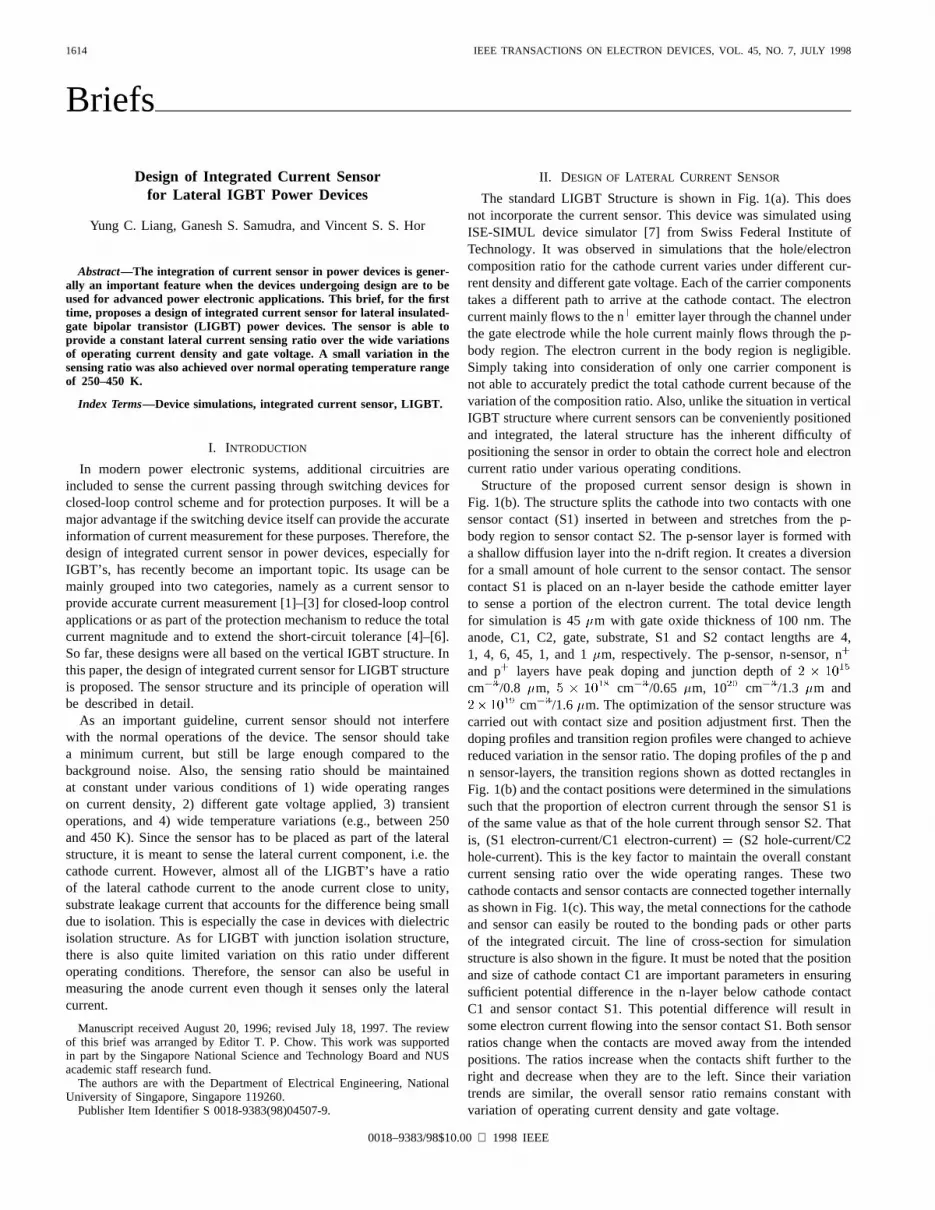
The standard LIGBT Structure is shown in Fig. 1(a). This doesnot incorporate the current sensor. This device was simulated usingISE-SIMUL device simulator [7] from Swiss Federal Institute ofTechnology. It was observed in simulations that the hole/electroncomposition ratio for the cathode current varies under different cur-rent density and different gate voltage. Each of the carrier componentstakes a different path to arrive at the cathode contact. The electroncurrent mainly flows to the n+ emitter layer through the channel underthe gate electrode while the hole current mainly flows through the p-body region. The electron current in the body region is negligible.Simply taking into consideration of only one carrier component isnot able to accurately predict the total cathode current because of thevariation of the composition ratio. Also, unlike the situation in verticalIGBT structure where current sensors can be conveniently positionedand integrated, the lateral structure has the inherent difficulty ofpositioning the sensor in order to obtain the correct hole and electroncurrent ratio under various operating conditions.
Structure of the proposed current sensor design is shown inFig. 1(b). The structure splits the cathode into two contacts with onesensor contact (S1) inserted in between and stretches from the p-body region to sensor contact S2. The p-sensor layer is formed witha shallow diffusion layer into the n-drift region. It creates a diversionfor a small amount of hole current to the sensor contact. The sensorcontact S1 is placed on an n-layer beside the cathode emitter layerto sense a portion of the electron current. The total device lengthfor simulation is 45�m with gate oxide thickness of 100 nm. Theanode, C1, C2, gate, substrate, S1 and S2 contact lengths are 4,1, 4, 6, 45, 1, and 1�m, respectively. The p-sensor, n-sensor, n+
and p+ layers have peak doping and junction depth of2 � 1015
cm�3/0.8 �m, 5 � 1018 cm�3/0.65 �m, 1020 cm�3/1.3 �m and
2� 1019 cm�3/1.6�m. The optimization of the sensor structure was
carried out with contact size and position adjustment first. Then thedoping profiles and transition region profiles were changed to achievereduced variation in the sensor ratio. The doping profiles of the p andn sensor-layers, the transition regions shown as dotted rectangles inFig. 1(b) and the contact positions were determined in the simulationssuch that the proportion of electron current through the sensor S1 isof the same value as that of the hole current through sensor S2. Thatis, (S1 electron-current/C1 electron-current)= (S2 hole-current/C2hole-current). This is the key factor to maintain the overall constantcurrent sensing ratio over the wide operating ranges. These twocathode contacts and sensor contacts are connected together internallyas shown in Fig. 1(c). This way, the metal connections for the cathodeand sensor can easily be routed to the bonding pads or other partsof the integrated circuit. The line of cross-section for simulationstructure is also shown in the figure. It must be noted that the positionand size of cathode contact C1 are important parameters in ensuringsufficient potential difference in the n-layer below cathode contactC1 and sensor contact S1. This potential difference will result insome electron current flowing into the sensor contact S1. Both sensorratios change when the contacts are moved away from the intendedpositions. The ratios increase when the contacts shift further to theright and decrease when they are to the left. Since their variationtrends are similar, the overall sensor ratio remains constant withvariation of operating current density and gate voltage.
0018–9383/98$10.00 1998 IEEE
IEEE TRANSACTIONS ON ELECTRON DEVICES, VOL. 45, NO. 7, JULY 1998 1615
(a)
(b)
(c)
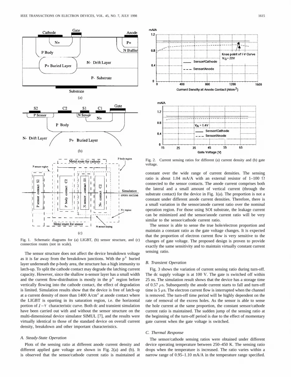
Fig. 1. Schematic diagrams for (a) LIGBT, (b) sensor structure, and (c)connection routes (not in scale).
The sensor structure does not affect the device breakdown voltageas it is far away from the breakdown junctions. With the p+ buriedlayer underneath the p-body area, the structure has a high immunity tolatch-up. To split the cathode contact may degrade the latching currentcapacity. However, since the shallow n-sensor layer has a small widthand the current flow-distribution is mostly in the p+ region beforevertically flowing into the cathode contact, the effect of degradationis limited. Simulation results show that the device is free of latch-upat a current density of more than 1400 A/cm2 at anode contact wherethe LIGBT is oparting in its saturation region, i.e. the horizontalportion ofI�V characteristic curve. Both dc and transient simulationhave been carried out with and without the sensor structure on themulti-dimensional device simulator SIMUL [7], and the results werevirtually identical to those of the standard device on overall currentdensity, breakdown and other important characteristics.
A. Steady-State Operation
Plots of the sensing ratio at different anode current density anddifferent applied gate voltage are shown in Fig. 2(a) and (b). Itis observed that the sensor/cathode current ratio is maintained at
Fig. 2. Current sensing ratios for different (a) current density and (b) gatevoltage.
constant over the wide range of current densities. The sensingratio is about 1.04 mA/A with an external resistor of 1–100connected to the sensor contacts. The anode current comprises boththe lateral and a small amount of vertical current (through thesubstrate contact) for the device in Fig. 1(a). The proportion is not aconstant under different anode current densities. Therefore, there isa small variation in the sensor/anode current ratio over the nominaloperation region. For those using SOI substrate, the leakage currentcan be minimized and the sensor/anode current ratio will be verysimilar to the sensor/cathode current ratio.
The sensor is able to sense the true hole/electron proportion andmaintain a constant ratio as the gate voltage changes. It is expectedthat the proportion of electron current flow is very sensitive to thechanges of gate voltage. The proposed design is proven to provideexactly the same sensitivity and to maintain virtually constant currentsensing ratio.
B. Transient Operation
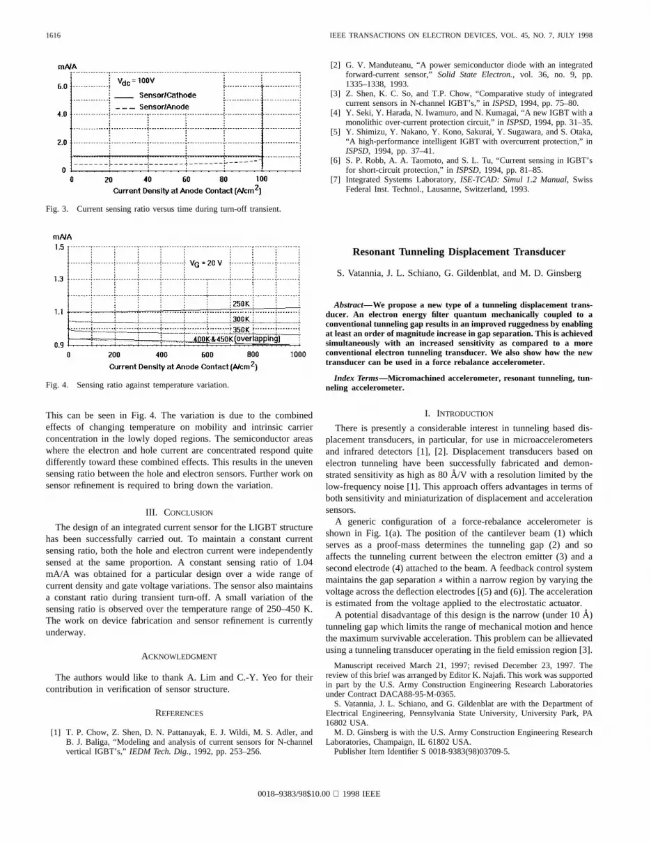
Fig. 3 shows the variation of current sensing ratio during turn-off.The dc supply voltage is at 100 V. The gate is switched off within25 ns. The simulation result shows that the device has a storage timeof 0.57�s. Subsequently the anode current starts to fall and turn-offtime is 5�s. The electron current flow is interrupted when the channelis removed. The turn-off time period will be highly dependent on therate of removal of the excess holes. As the sensor is able to sensethe hole current at the same proportion, the constant sensor/cathodecurrent ratio is maintained. The sudden jump of the sensing ratio atthe beginning of the turn-off period is due to the effect of momentarygate current when the gate voltage is switched.
C. Thermal Response
The sensor/cathode sensing ratios were obtained under differentdevice operating temperature between 250–450 K. The sensing ratiodrops when the temperature is increased. The ratio varies within anarrow range of 0.95–1.10 mA/A in the temperature range specified.
1616 IEEE TRANSACTIONS ON ELECTRON DEVICES, VOL. 45, NO. 7, JULY 1998
Fig. 3. Current sensing ratio versus time during turn-off transient.
Fig. 4. Sensing ratio against temperature variation.
This can be seen in Fig. 4. The variation is due to the combinedeffects of changing temperature on mobility and intrinsic carrierconcentration in the lowly doped regions. The semiconductor areaswhere the electron and hole current are concentrated respond quitedifferently toward these combined effects. This results in the unevensensing ratio between the hole and electron sensors. Further work onsensor refinement is required to bring down the variation.
III. CONCLUSION
The design of an integrated current sensor for the LIGBT structurehas been successfully carried out. To maintain a constant currentsensing ratio, both the hole and electron current were independentlysensed at the same proportion. A constant sensing ratio of 1.04mA/A was obtained for a particular design over a wide range ofcurrent density and gate voltage variations. The sensor also maintainsa constant ratio during transient turn-off. A small variation of thesensing ratio is observed over the temperature range of 250–450 K.The work on device fabrication and sensor refinement is currentlyunderway.
ACKNOWLEDGMENT
The authors would like to thank A. Lim and C.-Y. Yeo for theircontribution in verification of sensor structure.
REFERENCES
[1] T. P. Chow, Z. Shen, D. N. Pattanayak, E. J. Wildi, M. S. Adler, andB. J. Baliga, “Modeling and analysis of current sensors for N-channelvertical IGBT’s,” IEDM Tech. Dig., 1992, pp. 253–256.
[2] G. V. Manduteanu, “A power semiconductor diode with an integratedforward-current sensor,”Solid State Electron., vol. 36, no. 9, pp.1335–1338, 1993.
[3] Z. Shen, K. C. So, and T.P. Chow, “Comparative study of integratedcurrent sensors in N-channel IGBT’s,” inISPSD, 1994, pp. 75–80.
[4] Y. Seki, Y. Harada, N. Iwamuro, and N. Kumagai, “A new IGBT with amonolithic over-current protection circuit,” inISPSD, 1994, pp. 31–35.
[5] Y. Shimizu, Y. Nakano, Y. Kono, Sakurai, Y. Sugawara, and S. Otaka,“A high-performance intelligent IGBT with overcurrent protection,” inISPSD, 1994, pp. 37–41.
[6] S. P. Robb, A. A. Taomoto, and S. L. Tu, “Current sensing in IGBT’sfor short-circuit protection,” inISPSD, 1994, pp. 81–85.
[7] Integrated Systems Laboratory,ISE-TCAD: Simul 1.2 Manual, SwissFederal Inst. Technol., Lausanne, Switzerland, 1993.
Resonant Tunneling Displacement Transducer
S. Vatannia, J. L. Schiano, G. Gildenblat, and M. D. Ginsberg
Abstract—We propose a new type of a tunneling displacement trans-ducer. An electron energy filter quantum mechanically coupled to aconventional tunneling gap results in an improved ruggedness by enablingat least an order of magnitude increase in gap separation. This is achievedsimultaneously with an increased sensitivity as compared to a moreconventional electron tunneling transducer. We also show how the newtransducer can be used in a force rebalance accelerometer.
Index Terms—Micromachined accelerometer, resonant tunneling, tun-neling accelerometer.
I. INTRODUCTION
There is presently a considerable interest in tunneling based dis-placement transducers, in particular, for use in microaccelerometersand infrared detectors [1], [2]. Displacement transducers based onelectron tunneling have been successfully fabricated and demon-strated sensitivity as high as 80A/V with a resolution limited by thelow-frequency noise [1]. This approach offers advantages in terms ofboth sensitivity and miniaturization of displacement and accelerationsensors.
A generic configuration of a force-rebalance accelerometer isshown in Fig. 1(a). The position of the cantilever beam (1) whichserves as a proof-mass determines the tunneling gap (2) and soaffects the tunneling current between the electron emitter (3) and asecond electrode (4) attached to the beam. A feedback control systemmaintains the gap separations within a narrow region by varying thevoltage across the deflection electrodes [(5) and (6)]. The accelerationis estimated from the voltage applied to the electrostatic actuator.
A potential disadvantage of this design is the narrow (under 10A)tunneling gap which limits the range of mechanical motion and hencethe maximum survivable acceleration. This problem can be allievatedusing a tunneling transducer operating in the field emission region [3].
Manuscript received March 21, 1997; revised December 23, 1997. Thereview of this brief was arranged by Editor K. Najafi. This work was supportedin part by the U.S. Army Construction Engineering Research Laboratoriesunder Contract DACA88-95-M-0365.
S. Vatannia, J. L. Schiano, and G. Gildenblat are with the Department ofElectrical Engineering, Pennsylvania State University, University Park, PA16802 USA.
M. D. Ginsberg is with the U.S. Army Construction Engineering ResearchLaboratories, Champaign, IL 61802 USA.
Publisher Item Identifier S 0018-9383(98)03709-5.
0018–9383/98$10.00 1998 IEEE