Embed Size (px)
Citation preview
Wireless Engineering and Technology, 2012, 3, 90-95 http://dx.doi.org/10.4236/wet.2012.32015 Published Online April 2012 (http://www.SciRP.org/journal/wet)
Design of Low Power and High Speed CMOS Comparator for A/D Converter Application
Shubhara Yewale, Radheshyam Gamad
Department of Electronics & Instrumentation Engineering, Shri G. S. Institute of Technology and Science, Indore, India. Email: {rsgamad, shubhra.vlsi}@gmail.com Received May 12th, 2011; revised July 15th, 2011; accepted August 15th, 2011
ABSTRACT
This paper presents an improved method for design of CMOS comparator based on a preamplifier-latch circuit driven by a clock. Design is intended to be implemented in Sigma-delta Analog-to-Digital Converter (ADC). The main advan-tage of this design is capable to reduce power dissipation and increase speed of an ADC. The design is simulated in 0.18 μm CMOS Technology with Cadence environment. Proposed design exhibits good accuracy and a low power consump-tion about 102 μW with operating sampling frequency 125 MHz and 1.8 V supply. Simulation results are reported and compared with earlier work done and improvements are observed in this work. Keywords: CMOS Comparato; Low Power; High Speed; Sigma-Delta ADC and Cadence
1. Introduction
Comparator is widely used in the process of converting analog signals to digital signals. In the A/D conversion process, it is necessary to first sample the input. This sampled signal is than applied to a combination of com-parators to determine the digital equivalent of the analog signal [1] and it compare the analog signal with another reference signal and outputs are binary signal based on the comparison. Low power and high speed ADCs are the main building blocks in the front-end of a radio-fre- quency receiver in most of the modem telecommunica-tion systems. As the comparator is one of the block which limits the speed of the converter, its optimization is of utmost importance. The preamplifier stage amplifies the input signal to improve the comparator sensitivity and isolate the input of the comparator from switching noise coming from positive feedback stage [2]. The latch stage is used to determine which of the input signals is larger and extremely amplifies their difference. The out-put buffer amplifies the information from latch and out-puts a digital signal [3]. The latched comparator is used for the clock signal and indicate digital output level, whether its differential input signal is positive or nega-tive. A positive feedback mechanism to regenerate the analog input signal into a full scale digital signal is much faster and power efficient than performing multi-stage linear applications [4]. The preamplifier latch comparator [5], which combines an amplifier and a latch comparator can be obtained high speed and low power dissipation. The amplifier which is added before the latch can reduce
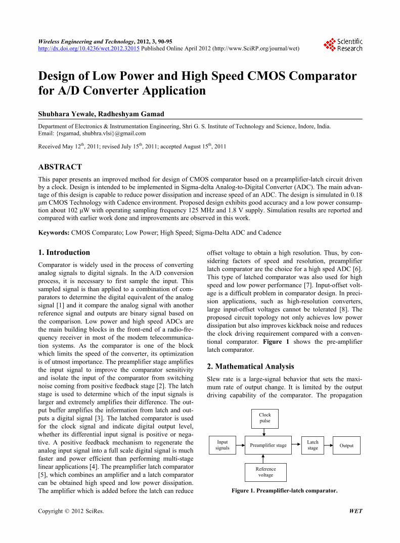
offset voltage to obtain a high resolution. Thus, by con-sidering factors of speed and resolution, preamplifier latch comparator are the choice for a high sped ADC [6]. This type of latched comparator was also used for high speed and low power performance [7]. Input-offset volt-age is a difficult problem in comparator design. In preci-sion applications, such as high-resolution converters, large input-offset voltages cannot be tolerated [8]. The proposed circuit topology not only achieves low power dissipation but also improves kickback noise and reduces the clock driving requirement compared with a conven-tional comparator. Figure 1 shows the pre-amplifier latch comparator.
2. Mathematical Analysis
Slew rate is a large-signal behavior that sets the maxi-mum rate of output change. It is limited by the output driving capability of the comparator. The propagation
Clock pulse
Preamplifier stage Input
signals Latch stage Output
Reference voltage
Figure 1. Preamplifier-latch comparator.
Copyright © 2012 SciRes. WET

Design of Low Power and High Speed CMOS Comparator for A/D Converter Application 91
delay is inversely proportional to the input voltage applied. This means that applying a larger input voltage will im-prove the propagation delay, up to the limits set by the slew rate [9].The most important dynamic parameters that determine the speed of a comparator are the propa-gation delay and the settling time. If the propagation de-lay time is determined by the slew rate of the comparator, then this time can be calculated as [10]:
2OH OL
p
V VVt T
SR SR
(1)
where, tp or ∆T = propagation delay ∆V = Change of the voltage at the output of the com-
parator SR = Slew rate VOH = Upper limit of the comparator VOL = Lower limit of the comparator If a square pulse is applied to the input of the com-
parator with a period T and frequency f, the average amount of current that the comparator must pull from VDD, recalling the current is being supplied from VDD only when p-channel is on. Notice that the power dissi-pation is a function of the clock frequency. A great deal of effort is put in to reducing the power dissipation of CMOS circuits. One of the major advantages of dynamic logic is its power dissipation [11]. Switched capacitor based comparator provides good accuracy of time con-stants but suffers from clock feed through and requires non-overlapping clock [12]. Approximately 180˚ out of phase two clock signals can be used to control amplifica-tion and reset of latch [13]. The proposed topology uses only one control signal to control both the operations as amplification and reset of latch.
2.1. Sampling Frequency
The sampling frequency “fsampling” is defined as the reciprocal of the time interval T, as [14]:
fsampling (2)
The sampling frequency has to be equal or greater than twice of the frequency bandwidth of analog signals.
2.2. Power Dissipation
Dynamic comparator power dissipation resembles that of digital gates, which have a power dissipation given ap-proximately by [15]:
2DDP fCV (3)
where, f is the output frequency, VDD is the supply voltage,
and C is the output capacitance.
3. Proposed Design
The proposed preamplifier consists of transistors M0 to M4. Since the input differential pair uses NMOS transis-tors M0 & M1, while the load transistor uses PMOS transistors M2 & M3, the gain of this preamplifier easily reach an acceptable value with small size of input differ-ential pair. The Latch is the most sensitive part in the comparator design. It consists of two inverters connected back to back with each other forming a differential com-parator and an NMOS transistor is connected between the two differential nodes of the latch. The schematic of latch consist of transistors M5 to M13 which includes cross coupled inverter pair M5-M6 & M7-M8 and the charge imbalance circuitry M9-M11. Transistors M5-M8 forms the main regenerative loop for the latch. For least capacitive effects, width and lengths of transistors M5-M8 are kept minimum and W/L ratio is kept as for an ideal inverter. Sizes are further optimized to set the metastable trip point of the inverter to half of the supply voltage. The switching transistor M11 short circuits the latch’s differential nodes to a common DC level. An ad-vantage of increasing its width is that it brings the DC level on both nodes close to each other. Transistors M9-M10 are used to avoid the clock feed through and kickback effects from the latch to the input. Width of these transistors also affects the performance of the latch. If the width is increased, it adds to the equivalent capaci-tance on the nodes of the latch and increases the effect of clock feed through on the input; resulting in degradation in sensitivity of the latch. If the width is decreased, then input signal has to be increased otherwise charge imbal-ance on the latch is not properly created. The latch oper-ates in two phases; reset and regeneration. In the Reset phase, the charge imbalance is created on the differential nodes of the latch proportional to the variation in the input signal. In regeneration mode, the voltage imbalance on the nodes is amplified to the rail-to-rail digital levels by the NMOS and PMOS regeneration loops.
When clk goes high, the amplifier is disabled and the latch is being to amplify the difference obtained at its input transistors M12-M13 to generate logic levels at the output. Figure 2 shows the schematic view of the pro- posed comparator design. In the design we have used 4 transistors (two NMOS-PMOS pair) in the inverter com- bination. This combination reduces the parasitic capaci- tance and hence high comparison speed can be achieved. During the reset phase, the switching transistor short cir- cuits the latch’s outputs and the output of that point is approximately equal to 1/2 power supply. The advantage for this characteristic is that in the second phase the re- generative loop can easily shift the output to the corre- sponding digital levels as determined by the charge im- balance. This also increases the speed and performance of the comparator.
Copyright © 2012 SciRes. WET

Design of Low Power and High Speed CMOS Comparator for A/D Converter Application
Copyright © 2012 SciRes. WET
92
4. Simulation Results and Discussions speed and low propagation delay are the main parameters. Simulation results of the Preamplifier are presented in Figure 3 which shows a DC gain of 19.5 dB. Figure 4 shows the ac response of Latch, when modeled as an inverter and the results are obtained as DC gain of 45 dB, unity gain frequency of 116.9 MHz. Finally simulation
Simulation of reported design is done using the 0.18 μm CMOS technology. In this design, we have used 1.8 V supply voltage for operation and clock period was 8ns. During the process, speed of the comparator was 125 MS/sec. This design can be used where low power, high
Figure 2. Schematic view of proposed comparator.
Figure 3. Gain response of preamplifier.

Design of Low Power and High Speed CMOS Comparator for A/D Converter Application 93
Figure 4. Gain response of Latch.
Figure 5. Results of a proposed design.
results of the comparator are given in Figure 5, when a differential sinusoidal signal is applied as an input to the latched comparator. The output here also changes its
orientation depending upon the input. In addition we have also reported the results of power dissipation in Figure 6. Table 1 shows th comparison of present re- e
Copyright © 2012 SciRes. WET

Design of Low Power and High Speed CMOS Comparator for A/D Converter Application 94
Figure 6. Result for power dissipation.
Table 1. Comparison of present results with earlier reported work.
References Technology (CMOS) Sampling rate Power dissipation Voltage supply
[11] 0.35 μm 40 MHz 200 μW 2 V
[12] 0.25 μm 100 MHz 153 μW 1.8 V
[13] 0.18 μm 100.5 MHz 132.7 μW 2 V
Present results 0.18 μm 125 MHz 102 μW 1.8 V
sults with earlier reported work and got improvement in this result.
5. Conclusion
This paper reports a CMOS comparator design and its simulation results for high speed and low power con-sumption. Present design is based on pre amplifier re-generation circuit and a latch. This comparator is de-signed for high resolution sigma delta ADCs. Simulation results are obtained with ±1.8 V power supply. We achieved the high sampling frequency of 125 MHz and low power consumption about 102 μW as compare to earlier reported work. Present results are compared and improvement is observed as shown in Table 1.
6. Acknowledgements
This work has been carried out in SMDP VLSI labora-tory of the Electronics and Instrumentation Engineering
Department of Shri G S Institute of Technology and Sci-ence, Indore, India. This SMDP VLSI project is funded by Ministry of Information and Communication Tech-nology, Government of India. Authors are thankful to the Ministry for facilities provided under this project.
REFERENCES [1] B. Razavi, “Deign of Analog CMOS Integrated Circuits,”
Tata McGraw-Hill, Delhi, 2002.
[2] R. Wang, K. Li, J. Zhang and B. Nie, “A High Speed High Resolution Latch Comparator For-Pipeline ADC,” IEEE International Workshop on Anti-counterfeiting, Se- curity, Identification, Xiamen, 16-18 April 2007, pp. 28- 31.
[3] W. Rong, W. Xiaobo and Y. Xiaolang, “A Dynamic CMOS Comparator with High Precision and Resolution,” IEEE Proceedings of 7th International Conference on So- lid-State and Integrated Circuits Technology, 18-21 Oc- tober 2004, pp. 1567-1570.
Copyright © 2012 SciRes. WET
Design of Low Power and High Speed CMOS Comparator for A/D Converter Application 95
[4] J. Wu, “A 100-MHz Pipelined CMOS Comparator,” IEEE Journal of Solid State Circuits, Vol. 23, No. 6, 1988, pp. 1379-1385. doi:10.1109/4.90034
[5] J. M. Kim, “A 6-Bit 1.3 GSample/s A/D Converter in 0.35 μm CMOS,” Doctor Thesis, University of Texas at Dallas, Dallas, 2005.
[6] G. Yongheng, C. Wei, L. Tiejun and W. Zongmin, “A Novel 1GSPS Low Offset Comparator for High Speed ADC,” 5th International Joint Conference on INC, IMC and IDC, IEEE Computer Society, Seoul, 25-27 August 2009, pp. 1251-1254.
[7] D. A. Johns and K. Martin, “Analog Integrated Circuit Design,” John Wiley and Sons, Inc., New York, 1997.
[8] A. Mohan, A. Zayegh, A. Stoiceyski and R. Veljanoyski, “Comparator for High Speed Low Power Ultra Wideband A/D Converter”, International Conference on Communi- cation, Computer and Power (ICCCP), Muscat, 19-21 February 2007, pp. 1-5.
[9] P. R. Gray and R. G. Meyer, “Analysis and Design of Analog Integrated Circuits,” 3rd Edition, John Wiley & Sons, Inc., Hoboken, 1993.
[10] P. E. Allen and D. R. Holberg, “CMOS Analog Circuit
Design,” 2nd Edition, Oxford University, Oxford, 2007.
[11] Y. Degerli, N. Fourches, M. Rouger and P. Lut, “Low Power Autozeroed High-Speed Comparator for the Read- out Chain of a CMOS Monolithic Active Pixel Sensor Based Vertex Detector,” IEEE Transactions on Nuclear Science, Vol. 50, No. 5, 2003, pp. 1-21.
[12] Y. Sun, Y. S. Wang and F. C. Lai, “Low Power High Speed Switched Current Comparator,” IEEE 14th Inter- national Conference, Ciechocinek, 21-23 June 2007, pp. 305-308.
[13] M. Panchore and R. S. Gamad, “Low Power and High Speed CMOS Comparator Design Using 0.18 μm Tech- nology,” International Journal of Electronic Engineering Research, Research India Publications, Vol. 2, No. 1, 2010, pp. 71-77.
[14] H. Nyquist, “Certain Topics in Telegraph Transmission Theory,” Transactions of the AIEE, Vol. 47, No. 2, 1928, pp. 617-644.
[15] C. Wulff and T. Ytterdal, “0.8V 1GHz Dynamic Com- parator in Digital 90nm CMOS Technology,” IEEE 23rd NORCHIP Conference, 21-22 November 2005, pp. 237- 240.
Copyright © 2012 SciRes. WET