Embed Size (px)
Citation preview

i
DESIGN OF MICROSTRIP ANTENNA BASED ON DIFFERENT
MATERIAL PROPERTIES
ANIS NABIHAH BINTI IBRAHIM
A project report submitted in partial fulfillment of the requirement
for the degree of
Master of Electrical Engineering
Faculty of Electrical and Electronics Engineering
Universiti Tun Hussein Onn Malaysia
JANUARI 2015
v
ABSTRACT
Microstrip antenna has several advantages compared to conventional microwave
antenna. These type of antenna are light weight, low volume and thin profile
configurations, which can be made conformal. The cost of fabrication is also low and
can be manufactured in a large quantities. This project will discuss about the microstrip
antenna. The aim of this project is to design a microstrip antenna by using Flame
Retardant 4 (FR4) substrate and Roger 4350 substrate which will be operating in
Wireless Local Area Network (WLAN). The frequency chosen for the microstrip
antenna is 2.4GHz and it has been chosen from IEEE 802.11 which is for the Wireless
Fidelity (WiFi) network. This project is divided into three major parts which are
calculation, simulation and hardware design. Computer Simulation Technology (CST)
microwave studio software used to analyze the radiation pattern of the antenna before
fabricated the antenna. Vector Network Analyzer (VNA) used to measure the fabricated
antenna to obtain the measurement result. The simulation and measurement results
shows a little bit differences for both of the material substrates. Comparison between
simulation and measurement result has been made.

vi
ABSTRAK
Antena Mikrojalur mempunyai beberapa kelebihan berbanding dengan Antena
Gelombang Mikro Konvensional. Antenna Mikrojalur mempunyai kos fabrikasi yang
rendah dan boleh dihasilkan dalam kuantiti yang banyak. Projek ini memfokuskan kajian
tentang Antena Mikrojalur dan untuk merekabentuk antena tersebut dengan
menggunakan FR4 dan Roger4350. Frekuensi yang dipilih bagi antenna ini adalah
2.4GHz yang telah dipilih dari IEEE 802.11 bagi rangkaian WiFi. Projek ini dibahagikan
kepada tiga bahagian utama iaitu pengiraan, simulasi dan fabrikasi. Perisian komputer
yang digunakan bagi merekabentuk antena ini adalah CST dan digunakan untuk
menganalisis corak sinaran antena sebelum difabrikasi. VNA digunakan untuk
mengukur antenna yang telah difabrikasi bagi memastikan antena tersebut boleh
berfungsi dalam frekuensi yang telah ditetapkan. Keputusan simulasi dan pengukuran
mununjukkan terdapat sedikit perbezaan bagi kedua-dua jenis bahan yang digunakan.
Perbandingan diantara hasil simulasi dan hasil pengukuran telah dibuat.

vii
CONTENTS
TITLE i
DECLARATION ii
DEDICATION iii
ACKNOWLEDGEMENT iv
ABSTRACT v
ABSTRAK vi
TABLE OF CONTENTS vii
LIST OF TABLE x
LIST OF FIGURE
LIST OF SYMBOL AND ABBREVIATIONS
xi
xvi
LIST OF APPENDIX xvii
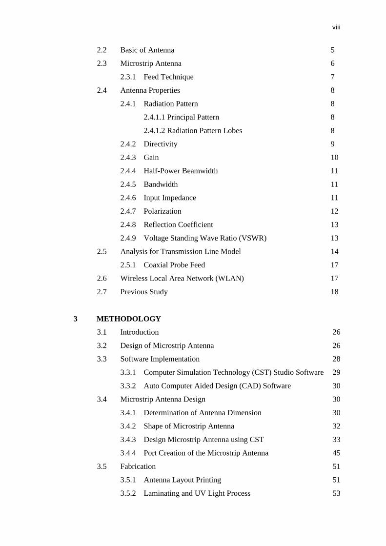
1 INTRODUCTION
1.1 Background Study 1
1.2 Problem Statements 3
1.3 Objectives 4
1.4 Scope 4
2 LITERATURE REVIEW
2.1 Overview 5
viii
2.2 Basic of Antenna 5
2.3 Microstrip Antenna 6
2.3.1 Feed Technique 7
2.4 Antenna Properties 8
2.4.1 Radiation Pattern 8
2.4.1.1 Principal Pattern 8
2.4.1.2 Radiation Pattern Lobes 8
2.4.2 Directivity 9
2.4.3 Gain 10
2.4.4 Half-Power Beamwidth 11
2.4.5 Bandwidth 11
2.4.6 Input Impedance 11
2.4.7 Polarization 12
2.4.8 Reflection Coefficient 13
2.4.9 Voltage Standing Wave Ratio (VSWR) 13
2.5 Analysis for Transmission Line Model 14
2.5.1 Coaxial Probe Feed 17
2.6 Wireless Local Area Network (WLAN) 17
2.7 Previous Study 18
3 METHODOLOGY
3.1 Introduction 26
3.2 Design of Microstrip Antenna 26
3.3 Software Implementation 28
3.3.1 Computer Simulation Technology (CST) Studio Software 29
3.3.2 Auto Computer Aided Design (CAD) Software 30
3.4 Microstrip Antenna Design 30
3.4.1 Determination of Antenna Dimension 30
3.4.2 Shape of Microstrip Antenna 32
3.4.3 Design Microstrip Antenna using CST 33
3.4.4 Port Creation of the Microstrip Antenna 45
3.5 Fabrication 51
3.5.1 Antenna Layout Printing 51
3.5.2 Laminating and UV Light Process 53

ix
3.5.3 Developing Process 54
3.5.4 Etching Process 54
3.5.5 Stripping Process 55
3.5.6 Soldering Process 55
3.6 Measurement 56
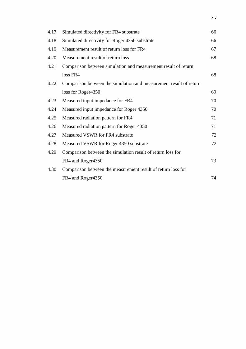
4 RESULT AND ANALYSIS
4.1 Simulation Result 57
4.1.1 Antenna Geometry Construction Parameters 58
4.1.2 Return Loss 58
4.1.3 Input Impedance 59
4.1.4 Voltage Standing Wave Ratio (VSWR) 60
4.1.5 Bandwidth 61
4.1.6 Radiation Pattern 62
4.1.7 Gain 65
4.1.8 Directivity 66
4.2 Measurement Result 67
4.2.1 Return Loss 67
4.2.2 Input Impedance 69
4.2.3 Radiation Pattern 70
4.2.4 Voltage Standing Wave Ratio (VSWR) 71
4.3 Comparison between FR4 and Roger4350 73
5 CONCLUSION AND RECOMMENDATION
5.1 Conclusion 76
5.2 Recommendation of Future Work 77
REFERENCES 78
APPENDIX
A
B

x
LIST OF TABLE
Table no Pages
2.1 Comparison between different substrate 19
2.2 Circular polarized microstrip patch antenna results 24
3.1 Material characteristic of dielectric constant and height 31
3.2 Antenna dimension based on difference material 31
4.1 Final dimension of antenna design parameters 58
4.2 Comparison between FR4 and Roger4350 75

xi
LIST OF FIGURE
Figures no Page
Chapter 1
1.1 Side view of microstrip patch antenna 3
Chapter 2
2.1 Microstrip Patch Antenna Structure 6
2.2 Coaxial Feed of the Antenna 7
2.3 Radiation Pattern of a Generic Directional Antenna 9
2.4 A Rectangular Microstrip Patch Antenna 14
2.5 A patch excited using coaxial cable 15
2.6 Feed Point for a Probe Fed-Patch 17
2.7 Antenna Design 20
2.8 S-Parameter Magnitude in dB (Return loss) 21
2.9 Layout of the one-sided directional slot antenna 21
2.10 Comparison of the measured and simulated return loss of this antenna 22
2.11 Proposed Antenna Layout design and Photograph of a
Patch Antenna on FR4 PCB 22
2.12 Simulated result of return loss characteristic 23
2.13 Measured results of return loss 23
2.14 The proposed geometry of patch antenna 24
2.15 S11 Parameter vs Frequency Plot 25
Chapter 3
3.1 Flowchart of the overall project 27

xii
3.2 Microstrip antenna design 32
3.3 CST Microwave Studio 33
3.4 Workspace of the CST Microwave Studio 34
3.5 List of antenna design dimension 34
3.6 Local Coordinate system 35
3.7 Working plane of antenna design 35
3.8 Parameter of substrate 36
3.9 Material library window show material list 37
3.10 Substrate Design 37
3.11 Bottom part view of Antenna Design 38
3.12 Pick Face to highlight Face 38
3.13 Bottom substrate face highlighted 39
3.14 Local Coordinate Aligned 39
3.15 Ground Plane parameter design 40
3.16 Ground Plane Shape 40
3.17 Front Face of substrate 41
3.18 Local Coordinate system of front face substrate 41
3.19 Parameter of Patch Design 41
3.20 Patch design 42
3.21 Parameter for Empty space 42
3.22 Shape intersection window 43
3.23 Empty space on patch of the antenna design 43
3.24 Microstrip Line design 44
3.25 Microstrip Line create on front face 44
3.26 Navigation Tree part 44
3.27 Patch and microstrip line of antenna design 45
3.28 Zoom image 45
3.29 Port Design 46
3.30 Waveguide Port 46
3.31 Waveguide Port Window 46
3.32 Port system of Antenna design 47
3.33 Units Window 47
3.34 Frequency range setting 48
3.35 H-Field and Surface current 48

xiii
3.36 Farfield/RCS 49
3.37 Time Domain Solver 49
3.38 Time Domain Solver Parameter Window 50
3.39 Progress Part of the Simulation Process 50
3.40 Message Part of the Simulation Process 50
3.41 Pick Face on modelling menu 51
3.42 Pick Face on patch and substrate 52
3.43 Save as DXF format 52
3.44 Printed Layout of the antenna design 53
3.45 Laminating Process 53
3.46 Developing Machine 54
3.47 Etching Machine 54
3.48 Stripping Machine 55
3.49 Soldering Process of antenna feed 55
3.50 Vector Network Analyzer (VNA) 56
3.51 Anechoic Chamber Room 56
Chapter 4
4.1 Simulation result of return loss for FR4 59
4.2 Simulation result of return loss for Roger 4350 59
4.3 Simulation result of smith Chart for FR4 60
4.4 Simulation result of smith Chart for Roger4350 60
4.5 Simulation result of VSWR for FR4 61
4.6 Simulation result of VSWR for Roger 4350 61
4.7 Simulation result of Bandwidth for FR4 62
4.8 Simulation result of Bandwidth for Roger 4350 62
4.9 3D radiation pattern for FR4 63
4.10 3D radiation pattern for Roger 4350 63
4.11 E-Plane for FR4 substrate 63
4.12 E-Plane for Roger 4359 64
4.13 H-Plane for FR4 substrate 64
4.14 H-Plane for Roger 4350 substrate 65
4.15 Simulated gain for FR4 substrate 65
4.16 Simulated gain for Roger 4350 substrate 66
xiv
4.17 Simulated directivity for FR4 substrate 66
4.18 Simulated directivity for Roger 4350 substrate 66
4.19 Measurement result of return loss for FR4 67
4.20 Measurement result of return loss 68
4.21 Comparison between simulation and measurement result of return
loss FR4 68
4.22 Comparison between the simulation and measurement result of return
loss for Roger4350 69
4.23 Measured input impedance for FR4 70
4.24 Measured input impedance for Roger 4350 70
4.25 Measured radiation pattern for FR4 71
4.26 Measured radiation pattern for Roger 4350 71
4.27 Measured VSWR for FR4 substrate 72
4.28 Measured VSWR for Roger 4350 substrate 72
4.29 Comparison between the simulation result of return loss for
FR4 and Roger4350 73
4.30 Comparison between the measurement result of return loss for
FR4 and Roger4350 74
xvi
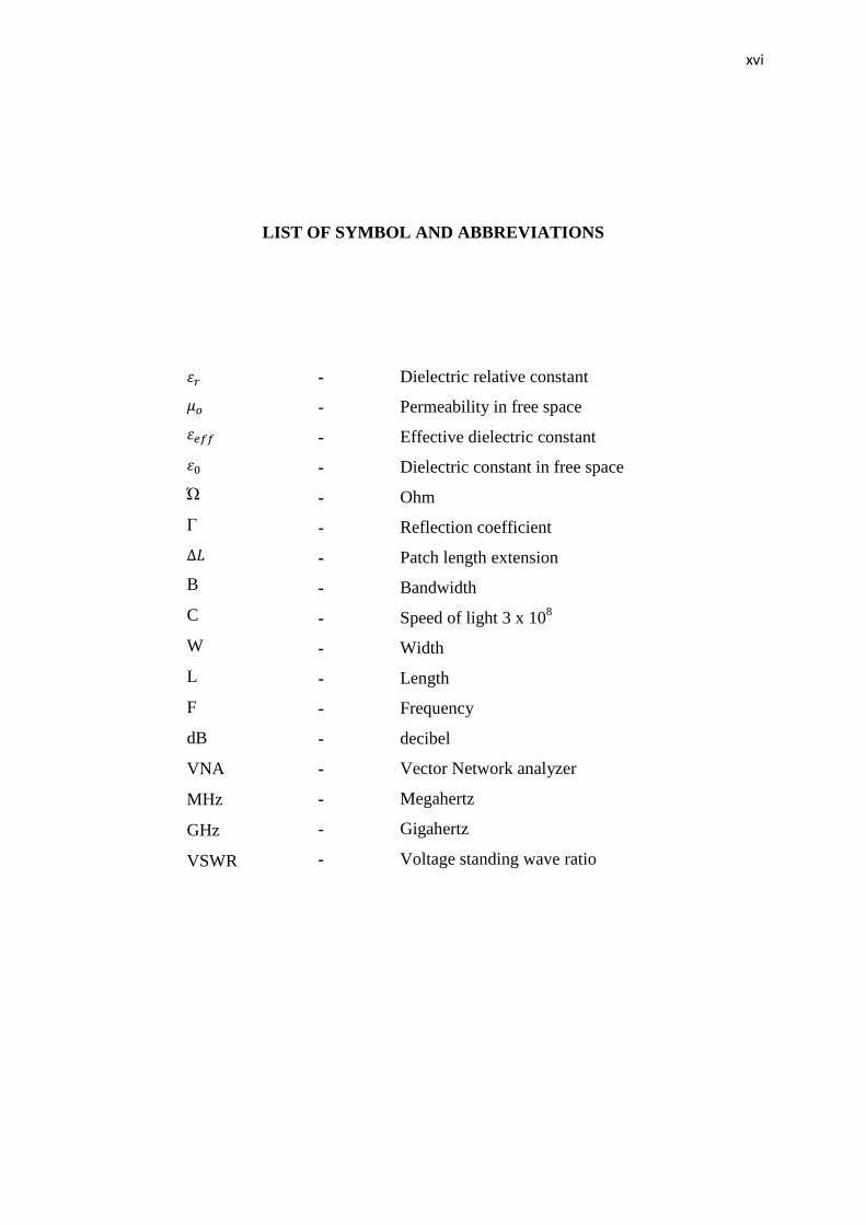
LIST OF SYMBOL AND ABBREVIATIONS
Ώ
Γ
B
C
W
L
F
dB
VNA
MHz
GHz
VSWR
-
-
-
-
-
-
-
-
-
-
-
-
-
-
-
-
-
Dielectric relative constant
Permeability in free space
Effective dielectric constant
Dielectric constant in free space
Ohm
Reflection coefficient
Patch length extension
Bandwidth
Speed of light 3 x 10⁸
Width
Length
Frequency
decibel
Vector Network analyzer
Megahertz
Gigahertz
Voltage standing wave ratio

xvii
LIST OF APPENDIX
NO TITLE PAGE
A Gantt Chart PS1 and PS2 80
B Data of Simulation and Measurement Result 82
1
CHAPTER 1
INTRODUCTION
1.1 Background of Study
In high-performance like aircraft, spacecraft, satellite and missile application,
where sizes, weight, cost, performance, ease of installation, and aerodynamic profile are
constraints, low profile antenna may be required. Presently there are many other
government and commercial application, such as mobile radio and wireless
communications, which have similar specifications. Microstrip patch antenna can be
used based on these requirements. This antenna are low profile, conformable to planar
and non-planar surface, simple and low cost to manufacture by using a modern printed-
circuit technology. Microstrip antennas consist of a patch of metallization on a grounded
substrate. These are low-profile, lightweight antennas, most suitable for aerospace and
mobile applications. Because of their low-power handling capability, these antenna can
be used in low-power transmitting and receiving applications [1].
Wireless technology is a truly revolutionary paradigm shift, enabling multimedia
communication between people and devices from any location. Wireless
communications is by any measure, the fastest growing segment of the communications
industry. As such, it has captured the attention of the media and the imagination of the
public [2]. Modern wireless communication systems require low profile, lightweight,

2
high gain and simple structure antennas to assure reliability, mobility and high
efficiency. There are many parameters are important in designing the microstrip antenna.
Dielectric substrate is the main parameter in design purpose.
One types of wireless communication at 2.4GHz is Wireless Fidelity (WiFi). It is
enable devices such as smartphone, personal computer, video game console or digital
audio player can connect to the internet if within range of a wireless network connected
to the internet. The microstrip antenna was drawn the maximum attention of the antenna
community in recent year. A microstrip antenna is very simple in construction using a
conventional microstrip fabrication technique. Microstrip antennas consist of a patch of
metallization on a grounded electric substrate. There are low profiles, lightweight
antennas, most suitable for aerospace and mobile applications. The conducting patch can
be any shape but the most commonly used configurations are circular and rectangular
configurations.
Deschamps first proposed the concept of microstrip antennas in 1953 but
practical antennas were developed by Munson and Howell in 1970s [3]. Increasing
requirements for personal and mobile communications has made the microstrip antennas
very important. Microstrip antenna are becoming a popular choice for portable wireless
system since they are light weight, low cost and easily manufacturable [4].
It is also can be applied in Wireless Local Area Network (WLAN) application.
Wireless Local Area Networks (WLANs) use electromagnetic radio waves to transmit
data between computers in a Local Area Network (LAN), without the limitations set by
wired network cable or phone wire connection. These 802.11 Wireless Local Area
Network (WLAN) systems may operate at 2.4GHz [4].
Microstrip patch antenna can take a variety of forms, but the basic element
consists of a single patch of conductor on the upper surface of a grounded dielectric
substrate. The patch radiates efficiently when it is resonant, which generally means that

3
some characteristic dimension of the patch is nearly equal to one-half wavelength in the
substrate medium [5].
The shape of the patch can be rather arbitrary, but rectangular and circular
patches have several desirable characteristics and more often used in practice [5]. Figure
1.1 shows the side view of simple microstrip patch antenna. The simple microstrip
antenna consists of three layers which are substrate, patch layer and ground layer.
Figure 1.1 : Side view of microstrip patch antenna.
1.2 Problem Statement
Antenna is develop in order to fulfill the problem occur and upgraded the antenna
for the advanced technologies. A conventional antenna is very hard to design compared
to microstrip antenna. A conventional antenna is very costly and quite heavy but the
microstrip patch antenna has a simple structure and quite easy to fabricated. There are
many shape of microstrip patch antenna such as rectangular, circular, triangular and
other types of geometries. The most popular configuration is rectangular microstrip
patch antenna. In order to produce antenna for Wireless Local Area Network (WLAN)
application, based on the factor, a rectangular microstrip patch antenna will be designed.
This project will used the Flame Retardant 4 (FR4) and Roger4350 as a dielectric
substrate in fabrication of the antenna.
Patch Layer
Substrate
Ground Layer
4
1.3 Objective
i. To design a microstrip antenna for Wireless Local Area Network (WLAN)
application with frequency of 2.4GHz.
ii. To simulate the antenna design by using Computer Simulation Technology
(CST) Microwave Studio.
iii. To fabricate the microstrip antenna by using Flame Retardant 4 (FR4) and
Roger4350 substrate.
iv. To investigate the performance of the antennas in term of return loss, operating
frequency, bandwidth and Voltage Standing Wave Ratio (VSWR).
1.4 Scope
The main scope of this project consist of two parts which is software and
hardware design. For the simulation part, a Computer Simulation Technology (CST)
Studio will be used in order to design a rectangular microstrip patch antenna. For the
hardware part, a rectangular microstrip patch antenna will be fabricated by using the
different materials which is Flame Retardant 4 (FR4) and Roger 4350. The Network
Analyzer will be used to measure S11, input impedance and Voltage Standing Wave
Ratio (VSWR) while for the radiation pattern will be measured in anechoic chamber.

5
CHAPTER 2
LITERATURE REVIEW
2.1 Overview
This chapter reviews some similar previous work, related journals and researches
which include microstrip antenna design that can contribute an ideas for completing this
project. This chapters also will discuss about the performance of the antenna and the
material that has been used to fabricate the antenna. This chapter is very important to
know the performance of the antenna and to get a better performance of the antenna
compared to the conventional antenna.
2.2 Basic of Antenna
There are many basic types of antenna element such as the dipoles, horn, slot,
spiral, long wire, monopole, and there are also many different types of systems where
these element can be arrange in some form of an array, either fixed or electronically
controlled. Thus, the antenna can be divided into four types depends on their operating
frequency, characteristics and capability. The groups are resonant antenna, broadband
antenna, aperture antenna and electrically small antenna.
6
2.3 Microstrip Antenna
In its simplest configuration, microstrip antenna consist of radiating patch on one
side of a dielectric substrate which has a ground plane on the other side. The patch
conductors normally is copper or gold. The radiating patch and feeding lines is usually
photo etched at the dielectric substrate [6]. Figure 2.1 shows the structure of the
microstrip patch antenna.
Figure 2.1 : Microstrip Patch Antenna Structure.
Based on the Figure 2.1, it shows the common microstrip antenna structure
where W is the width of the patch, L is the length of the patch, t is the thickness of the
patch and h is the height of the substrate. To achieve the great in antenna performance, a
thick dielectric which have a low dielectric constant is needed. This will provide higher
efficiency, larger bandwidth and greater radiation. But, in order to achieve this, larger
antenna size will be produced. In order to reduce the size of the antenna which mean to
produce a compact design, a higher dielectric constant which is less efficient and will
contribute a narrower bandwidth will be used [6].
Microstrip antenna has several advantages compared to conventional microwave
antenna. These types of the antennas are light weight, low volume and thin profile
configurations, which can be made conformal. The cost of fabrication is also low. So, it
can be manufactured in a large quantities [6]. For the polarization types, it can support
L
W
Dielectric
Substrate
Ground
Plane
t
h
Patch
7
both linear and circular polarization depending on the radiation pattern. Microstrip patch
antenna also capable of dual and even triple frequency operations [6]. On the other hand,
microstrip patch antennas also have some disadvantages. These type of antenna have a
narrow bandwidth, low efficiency and also have a low gain [6].
2.3.1 Feed Techniques
Microstrip antenna feed techniques can be categorized in two categories which
are contacting and non-contacting. In the contacting method, the RF Power is fed
directly to the radiating patch using a connecting element such as a microstrip line. The
microstrip line and the coaxial probe are examples of contacting method.
In the non-contacting, electromagnetic field coupling will be done to transfer the
power between the microstrip line and the radiating patch. Techniques that are in these
non-contacting methods are aperture coupling and proximity coupling [6]. The feed
technique that was used in this project is the microstrip line feed. However, for the
coaxial feed, it can be placed at any location to match with its input impedance. It
provides narrow bandwidth and it is difficult to model. Figure 2.2 shows the coaxial feed
of the antenna [6].
Figure 2.2 : Coaxial Feed of the Antenna.
Dielectric
Substrate
Patch
Coaxial
Connector Ground
Plane

8
2.4 Antenna Properties
The performance of the antenna can be determine by this important parameters
which is radiation pattern, directivity, gain, half-power beamwidth, bandwidth, input
impedance, polarization, reflection coefficient, Voltage Standing Wave Ratio (VSWR)
and return loss.
2.4.1 Radiation Pattern
It is defined as a mathematical function or a graphical representation of the
radiation properties of the antenna as a function of space coordinates. The radiation
property of most concern is the two or three-dimensional spatial distribution of radiated
energy as the function of the observer’s position along a path of surface of constant
radius [7].
2.4.1.1 Principal Patterns
For a linearly polarized antenna, the performance is usually described in terms of
its principal E-plane and H-plane patterns. The E-plane is defined as the plane
containing the electric-field vector and the direction of maximum radiation. The H-plane
is defined as the plane containing the magnetic-field vector and the direction of
maximum [7].
2.4.1.2 Radiation Pattern Lobes
A radiation lobe is a portion of the radiation pattern bounded by regions of
relatively weak radiation intensity. A major lobe also called as the main beam is defined
as the radiation lobe containing the direction of maximum radiation. A minor lobe is any

9
lobe except a major lobe. A side lobe is a radiation lobe in any direction other than the
intended lobe. Usually a side lobe is adjacent to the main lobe and occupies the
hemisphere in the direction of the main beam. A back lobe is a radiation lobe which the
axis makes an angle of approximately 180 degrees with respect to the beam of an
antenna [7]. Figure 2.3 shows the radiation patter of a generic directional antenna.
Figure 2.3 : Radiation Pattern of a Generic Directional Antenna.
2.4.2 Directivity
Directivity can be defined as the ratio of the radiation intensity in a given
direction from the antenna to the radiation intensity averaged of all directions. The
average radiation intensity is equal to the total power radiated by the antenna divided by
4π. If the direction is not specified, the direction of maximum radiation intensity is
implied [7]. If the direction is not specified, the direction of maximum radiation intensity
can be expressed as
(2.1)
Where
= directivity (dimensionless)
= maximum directivity (dimensionless)
Minor Lobes Main Lobe
Back
Lobe Side Lobe
Null
HPBW
10
= radiation intensity (W/unit solid angle)
= maximum radiation intensity (W/unit solid angle)
= radiation intensity of isotropic source (W/unit solid angle)
= total radiated power (W)
Reference antennas usually are isotropic radiator where the radiated energy is the
same in all direction and have directivity of 1. It can be defined as
(2.2)
Where
= maximum radiated energy
= isotropic radiator energy
2.4.3 Gain
Gain is closely related to directivity but it is measure that takes into account the
efficiency of the antenna and also the directional capabilities. Absolute gain of an
antenna in a given direction is defined as the ratio of the intensity, in a given direction,
to the radiation intensity that would be obtained if the power accepted by the antenna
were radiated isotropically. The radiation intensity corresponding to the isotropically
radiated power is equal to the power accepted by the antenna divided by 4π [7]. It is also
can be expressed as
(2.3)
For a lossless isotropic source, it can be determined by
11
(2.4)
2.4.4 Half-power Beamwidth
Half-power beamwidth can be defined as in a plane containing the direction of
the maximum of a beam, the angle between the two directions in which the radiation
intensity is one-half of the maximum value of the beam. It is used to describe the 3dB
beamwidth. As the beamwidth decreases, the side lobe increases and vice versa [7].
2.4.5 Bandwidth
The term of bandwidth is defines as the range of frequencies within which the
performance of the antenna, with respect to some characteristics, conforms to a specified
standard. For narrowband antenna, the bandwidth is expressed as a percentage of the
frequency difference over the center frequency of bandwidth. The characteristics such as
input impedance, gain and polarization of the antenna do not necessarily affect the
frequency. So, there is no unique characterization of the bandwidth. There are no
distinctions made between pattern and input impedance variations. Pattern bandwidth
and impedance bandwidth are used to emphasize this distinction. Gain, side lobe level,
beamwidth, polarization and beam direction are associated with pattern bandwidth while
input impedance and radiation efficiency are associated with impedance bandwidth [7].
Narrowband by percentage can be expressed by
(2.5)

12
2.4.6 Input Impedance
Input impedance can be defined as the impedance presented by the antenna at its
terminals or ratio of the voltage to current at a pair of the ratio of the appropriate
components of the electric to magnetic field at a point. The input impedance can be
determined by the maximum power transfer between transmission line and the antenna.
When the input impedance, antenna and transmission line are matched, the maximum
power transfer will be achieved. Reflected wave will be generated at the antenna
terminal and travel back towards the energy source if it is not matched. It will cause
reduction on overall system efficiency [7]. The input impedance can be described as
(2.6)
Where
= n input impedance
= characteristic impedance
= return loss
2.4.7 Polarization
Polarization of the antenna in a given direction is defined as the polarization of
the wave transmitted (radiated) by the antenna. The polarization of a wave can be
defined in terms of a wave radiated or received by the antenna in a given direction. The
polarization of a wave radiated by the antenna in a specified direction at a point in the
far field is defined as the polarization of the plane wave whose electric field strength is
the same as that of the wave and whose direction of propagation is in the radial direction
from the antenna [7].

13
Polarization can be classified as linear, circular and elliptical. The field is said to
be linearly polarized if the vector that describes the electric field at a point in space as a
function of time is always directed along a line. If the electric field traces is an ellipse,
the field is elliptical polarized. For circular polarization, a time-harmonic wave is
circularly polarized at a given point in space if the electric field or magnetic field vector
at that point traces a circle as a function of time [7].
Polarization characteristics of the antenna can be represented by its polarization
pattern which is defined as the spatial distribution of the polarizations of a field vector
excited by the antenna taken over its radiation sphere [7].
2.4.8 Reflection Coefficient
Determining the value of the input reflection coefficient of the antenna is
necessary to determine the location of the resonant bands. The input reflection
coefficient Γin, is obtained from expression below
(2.7)
Where
= input impedance of the antenna
= characteristic impedance used in the transmission line, as a reference
The absolute value of the reflection coefficient can be also expressed as the ratio
of the reflected power from the antenna input, Pin and the power delivered to the
antenna, Pin as in expression below
14
(2.8)
2.4.9 Voltage Standing Wave Ratio (VSWR) and Return Loss
When a load is mismatched to a transmission line, not all power from the
generator will be delivered to the load. The loss is called return and can be expressed by
(2.9)
A matched load, where the reflection coefficient, Γ=0 has returned loss of ∞dB,
whereas a total reflection of all power, where Γ=1, has a return loss of 0dB. In a
mismatched line, the presence of reflected wave leads to standing wave, where the
magnitude of the voltage oscillates along the line. As the value of reflection coefficient
increases, the ratio of the minimum and maximum voltages values (Vmax and Vmin)
also increases. So, the Voltage Standing Wave Ratio (VSWR) measures the ratio of
these voltages on a transmission line. It can be expressed by
(2.10)
For the antenna to be reasonably functional, a minimum SWR 1.5 ≤ is required.
2.5 Analysis for Transmission Line Model
The patch and ground-plane are separated by a dielectric. The patch conductor is
normally copper. The patches are usually photo-etched on the dielectric substrate. The
substrate is usually non-magnetic. The relative permittivity of the substrate is normally

15
in the region between 1 and 4, which enhances the fringing fields [8]. The rectangular
patch is characterized by its length L, width W and thickness h, as shown in figure 2.4
below.
Figure 2.4 : A Rectangular Microstrip Patch Antenna Showing Fringing Field that
Account for Radiation.
The inner conductor of the coaxial-line is connected to the radiating patch, while
the outer conductor is connected to the ground-plane, as shown in figure 2.5.
Figure 2.5 : A patch excited using coaxial cable.
An effective dielectric constant ( ) must be obtained in order to account for
the fringing and the wave propagation in the line. The value of is slightly less than
Patch Antenna
h Dielectric
Substrate
Ground Plane Coaxial
Connector
L
W
h Dielectric Substrate
Ground Plane
Patch

16
because the fringing fields around the periphery of the patch are not confined in the
dielectric substrate but are also spread in the air. It can be expressed by [9].
(2.11)
Where
= effective dielectric constant
= dielectric constant of a substrate
= height of dielectric substrate
= width of a patch
For a given resonance frequency ( ), the effective length is given by [9]
(2.12)
The fringing fields along the width can be modeled as radiating slots and
electrically the patch of the Microstrip antenna looks greater than its physical
dimensions. The dimensions of the patch along its length have now been extended on
each end by a distance, ∆L.
The ∆L can be expressed by [9]
(2.13)
The effective length of the patch now becomes
(2.14)
17
Where
= length due to fringing effects
= length of patch
= effective length of the patch
= height of dielectric substrate
= width of the patch
= effective dielectric constant
For efficient radiation, the width, W is given by [9]
(2.15)
Where
= operating frequency
= dielectric constant of a substrate
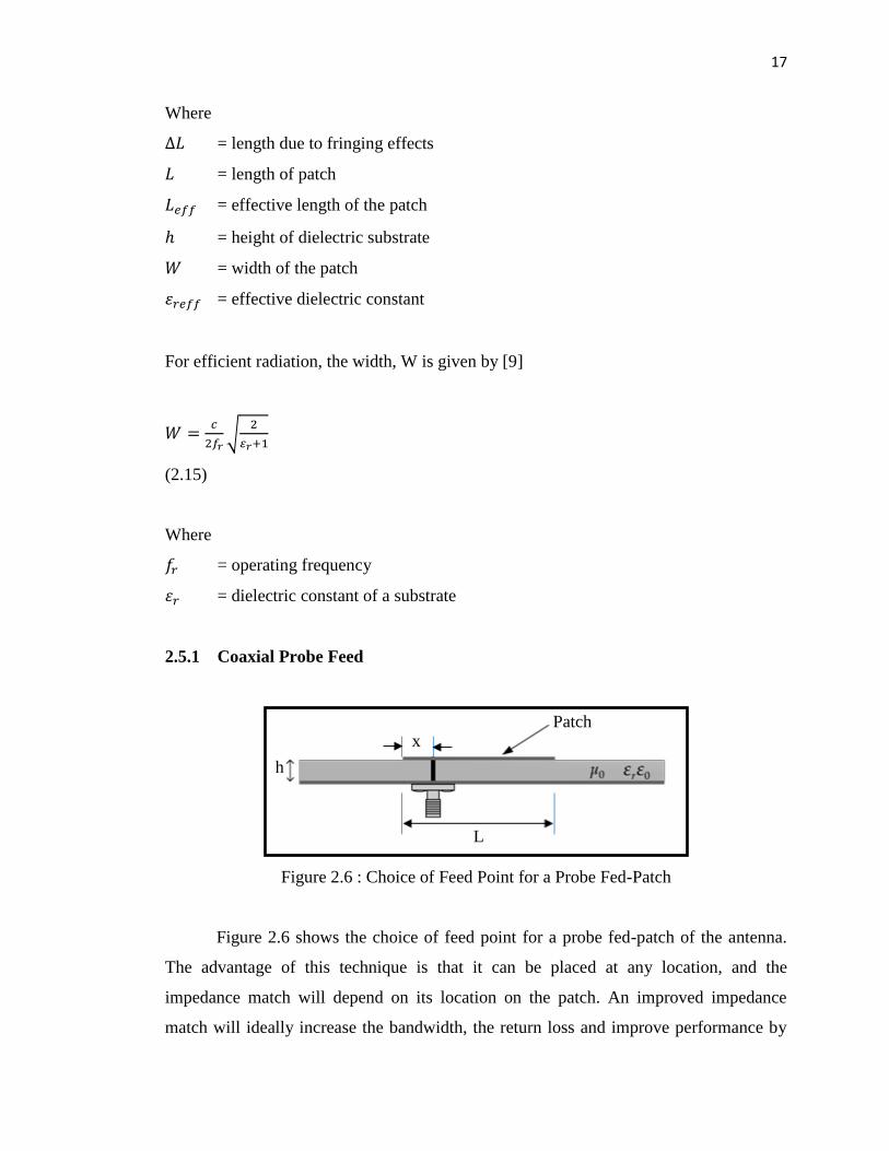
2.5.1 Coaxial Probe Feed
Figure 2.6 : Choice of Feed Point for a Probe Fed-Patch
Figure 2.6 shows the choice of feed point for a probe fed-patch of the antenna.
The advantage of this technique is that it can be placed at any location, and the
impedance match will depend on its location on the patch. An improved impedance
match will ideally increase the bandwidth, the return loss and improve performance by
Patch
L
h
x
18
reducing the excitation of unwanted modes of radiation. The feed coordinates were
calculated using the following equation [10].
(2.16)
(2.17)
2.6 Wireless Local Area Network (WLAN)
A Wireless Local Area Network (WLAN) is flexible data communication
network used as an extension to or an alternative for a wired Local Area Network (LAN)
in a building. Increasingly more and more Wireless Local Area Network (WLAN) are
being setup in home and or home office situations as the technology is becoming more
affordable [11].
The increasing popularity of indoor Wireless Local Area Network (WLAN)
capable of high-speed transfer rate is prompting the development of efficient broadband
antennas. Due to increased usage in residential and office areas, these systems are
required to be low profile, low cost as well as highly effective and efficient [11].
Microstrip patch antennas are well suited for Wireless Local Area Network (WLAN)
application systems due to their versatility, conformability, low cost and low sensitivity
to manufacturing tolerances. Conventionally patch antennas have showed a narrowband
response, implicating low bit rate transfer.
The most commonly used Wireless Local Area Network (WLAN) system is the
IEEE 802.11b system, with a maximum throughput of 11Mbps using a narrowband
system. Broadband refers to transmission of information using a system that uses a
comparatively larger frequency band, resulting in increases data transfer rate or
19
throughput. The broadband 802.11a system requires them to have a good coverage
without failing signal strength. The range of coverage is dependent directly on the
antenna performance hence the significance of the broadband antenna. A key
requirement of a Wireless Local Area Network (WLAN) system is that it should be low
profile, where it is almost invisible to the user. For this reason the microstrip patch
antennas are the antennas of choice for Wireless Local Area Network (WLAN) use [11].
2.7 Previous Work Study
This review is made focusing on the current project based on the previous
student’s work. This section describes the several of researches and projects that related
to microstrip patch antenna design. An extensive literature search in the area of
microstrip antenna for different substrate was conducted. It has been done to get some
idea for the project. The databases such as IEEE and Google scholar, which are a leading
source literature for antenna and engineering research, were used to complete the study.
Mostly the literature reviews that have been found are based on a previous researcher’s
technical papers from IEEE. The literature search is basically related on recent
performance of different substrate, simulation and experiment testing and model
updating on the antenna design. In this section, there are 6 papers that related to this
studied will be discussed.
Kiran Jain [12] have carried out a research for different substrate used in
microstrip patch antenna to enhance overall efficiency of antenna. Various substrates like
Foam, Duroid, Benzocyclobutane, Roger4350, Epoxy, Flame Retardant 4 (FR4) and
Duroid6010 are in use to achieve better gain and bandwidth. Another factor that impact
directly is loss tangent it shows inverse relation with efficiency the dilemma is here is
that substrate with lower loss tangent is costlier.
Substrates use in microstrip patch antenna varies from 2.2≤ ≤12. Lower the
permittivity of dielectric material larger the size of the antenna but it achieves better

20
efficiency and larger bandwidth. Table 2.1 shows the comparison between different
substrate.
Table 2.1: Comparison between different substrate.
Substrate r Loss
tangent
Resonance
frequency
Return Loss Gain
Benzocyclobutane 2.6 0 2.04GHz -18.124 5.5
Duroid 6010 10.7 0.00060 2.455GHz -9.449 4.02
Nylon fabric 3.6 0.0083 989MHz -35.42 6.11
Roger 4350 3.48 0.004 2.586GHz -25.29 4.62
RT-Duroid 2.2 0.0009 10GHz 12.03
Foam 1.05 0 454MHz -16.732 2.73
FR4 4.4 0.018 5.8GHz -14.73 9.8
The criterion for selection of right substrate is its price, efficiency and size.
Minimum size is achieved by using foam substrate but it is costlier and losses are higher
in it even the efficiency is much less than others. Maximum efficiency is achieved in
Roger4350 but the size and price are the issues in it. Than an optimal solution is FR4
substrate but it sometimes requirement dependent.
O.Bayarmaa [13] proposed to design mobile handset antenna for make mobile
handset more compact and thin. This antenna has an advantage of performing different
frequency bands by one antenna design. Design and simulations are done using CST
microwave Studio program. A Reconfigurable Antenna is designed by using the FR4
(lossy) substrate with the dielectric constant of r=4.3 and dielectric loss tangent 0.025.
The substrate thickness of h=1.6mm. This paper aim frequency between 0.9 GHz to
3.6GHz.
Antenna designers are always looking for creative ways to improve performance.
This antenna resembles an Inverted-F, which explains the Planar Inverted-F Antenna
21
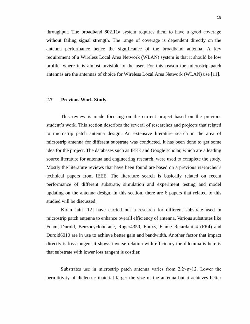
(PIFA) name. The Planar Inverted-F Antenna is popular because it has a low profile and
an omnidirectional pattern. The antenna design shown in Figure 2.7.
Figure 2.7: Antenna Design.
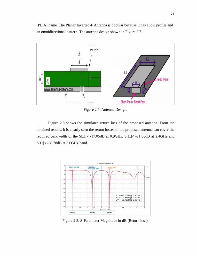
Figure 2.8 shows the simulated return loss of the proposed antenna. From the
obtained results, it is clearly seen the return losses of the proposed antenna can cover the
required bandwidth of the S|11|< -17.05dB at 0.9GHz, S|11|< -21.86dB at 2.4GHz and
S|11|< -38.78dB at 3.6GHz band.
Figure 2.8: S-Parameter Magnitude in dB (Return loss).
Patch
Shorting
Pin
Ground Plane Probe Feed

22
Haruichi Kanaya [14], in this paper describe the design of one-sided directional
slot antenna with quarter wavelength (λ/4) top metal layer, which is connected on the
bottom metal layer, for 2.4GHz-band application. By using the two resonances appeared
from the slot and λ/4 top metal, we can realize the one-sided directional radiation. We
designed and simulated the proposed antenna by using the commercial electro-magnetic
(EM) field simulator. This antenna is fabricated on FR4 printed circuit board and also
carried out experiments on this antenna. Figure 2.9 shows the layout of the one-sided
directional slot antenna with floating bottom metal layer. Cross sectional view of the
substrate is also shown, namely, conductor-baked configuration.
Figure 2.9: Layout of the one-sided directional slot antenna with λ/2 floating bottom
metal layer.
Figure 2.10 shows the simulated and measured return loss of this antenna. Center
frequency and bandwidth is almost the same values. We can obtain that the (S11) is
approximately more than 10dB, which is almost the same as that of simulated value.
23
Figure 2.10: Comparison of the measured and simulated return loss of this antenna.
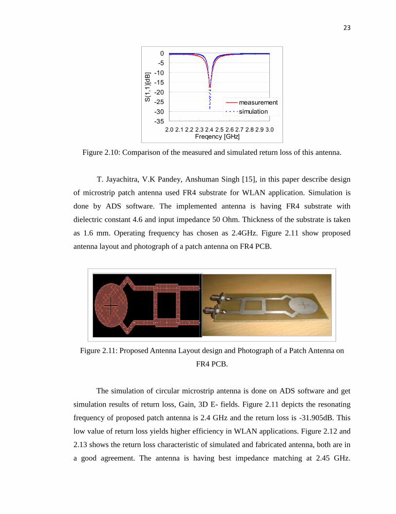
T. Jayachitra, V.K Pandey, Anshuman Singh [15], in this paper describe design
of microstrip patch antenna used FR4 substrate for WLAN application. Simulation is
done by ADS software. The implemented antenna is having FR4 substrate with
dielectric constant 4.6 and input impedance 50 Ohm. Thickness of the substrate is taken
as 1.6 mm. Operating frequency has chosen as 2.4GHz. Figure 2.11 show proposed
antenna layout and photograph of a patch antenna on FR4 PCB.
Figure 2.11: Proposed Antenna Layout design and Photograph of a Patch Antenna on
FR4 PCB.
The simulation of circular microstrip antenna is done on ADS software and get
simulation results of return loss, Gain, 3D E- fields. Figure 2.11 depicts the resonating
frequency of proposed patch antenna is 2.4 GHz and the return loss is -31.905dB. This
low value of return loss yields higher efficiency in WLAN applications. Figure 2.12 and
2.13 shows the return loss characteristic of simulated and fabricated antenna, both are in
a good agreement. The antenna is having best impedance matching at 2.45 GHz.
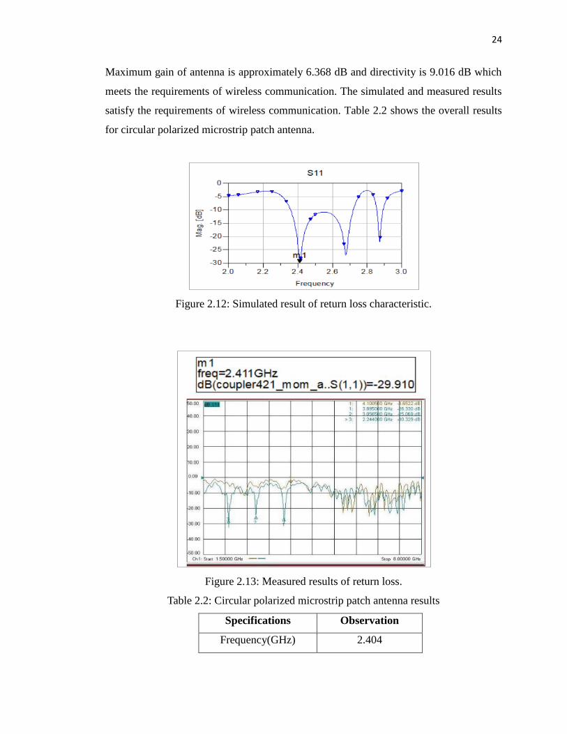
24
Maximum gain of antenna is approximately 6.368 dB and directivity is 9.016 dB which
meets the requirements of wireless communication. The simulated and measured results
satisfy the requirements of wireless communication. Table 2.2 shows the overall results
for circular polarized microstrip patch antenna.
Figure 2.12: Simulated result of return loss characteristic.
Figure 2.13: Measured results of return loss.
Table 2.2: Circular polarized microstrip patch antenna results
Specifications Observation
Frequency(GHz) 2.404
78
REFERENCES
[1] Ramesh Garg, Prakash Bhartia, Inder Bahl, Apisak Ittipiboon, “Microstrip Antenna
Design Handbook”, Artech House, 2001.
[2] Andrea Goldsmith, “Wireless Communication”, Cambridge University Press, 2005.
[3] Girish Kumar and K.P.Ray, “Broadband Microstrip Antenna”, Artech House Boston,
London, 2003.
[4] P. Nicopolitidis, “Wireless Communication System”, John Wiley, 2003.
[5] David M. Pozar and Daniel H. Schaubert, “Microstrip Antennas: The Analysis and
Design of Microstrip Antennas and Arrays”, John Wiley, 1995.
[6] Ahmad Mabrook Ali Saad, “Chapter 3, Dual-Band Microstrip Loop Antenna for
Wireless Application”, (Unpublished), 2013.
[7] Constantine A. Balanis, “Antenna Theory” (2nd
Edition) JohnWiley & Sons, INC,
Canada, 1997.
[8] J.R Jame,P.S Hall and C.Wood, “Microstrip Antenna Theory and Design”, London,
United Kingdom, Peter Peregrinus, 2006.
[9] Kraus, Marhefka, “Antenna for All Aplication”, (3rd
Edition), Ed. McGraw-Hill, 2002.
[10] Vajha.S and Prasad,S.N, “Design and Modelling of a Proximity Coupled Patch
Antenna”, Conference of on Antenna and Propagation for Wireless Communication,
2000.
[11] Mohammad Ilyas and Syed Ahson, “Handbook of Wireless Local Area Networks:
Applications, Technology, Security and Standards”, 2008.
[12] Kiran Jain, Keshav Gupta, “Different substrate use in microstrip patch antenna- A
Survey”, International Journal of Science and Research (IJSR), 2012.
[13] O. Bayarmaa, Kab-ki Kim, Young-Hun Lee, “Design of triple-band Planar Inverted-F
Antenna for 0.9/2.4/3.6GHz Wireless Application”, International Journal of
Multimedia and ubiquitous Engineering, 2014.
79
[14] Haruici Kanaya, Masataka Kato, R.K. Pokharel, Keiji Yoshida, “Development of
2.4GHz One-Sided Directional Planar Antenna with Quarter Wavelength Top Metal”,
Institute of Electrical and Electronic Engineering (IEEE), 2010.
[15] T. Jayachitra, V.K Pandey, Anshuman Singh, “Design of microstrip antenna for
WLAN application”, International Conference on Signal Processing, Embedded
System and Communication Technologies and their applications for Sustainable and
Renewable Energy (ICSECSRE), April 2014.
[16] Pradeep Kumar, Neha Thakur, Aman Sanghi, “Microstrip Patch Antenna for 2.4GHz
Wireless Applications”, International Journal of Engineering Trends and Technology
(IJETT), 2013.
[17] Tan Yee Mun, Chan Yee Kit, Koo Voon Chet Mohammad Tariqul Islam A “Novel
Wideband Antenna for Dual Band WLAN Application”, Institute of Electrical and
Electronic Engineering (IEEE), 2010.