Embed Size (px)
Citation preview
Design of nanostructured optical biosensors based on
metal-polymer nanopillars
Miguel Bernardo Trindade Simões da Silva Rosa
Thesis to obtain the Master of Science Degree in:
Bioengineering and Nanosystems
Supervisor: Prof. Dr. Carlos Angulo Barrios
Co-Supervisor: Prof. Dr. Luís Joaquim Pina da Fonseca
Examination Committee
Chairperson: Prof. Dr.Raúl Daniel Lavado Carneiro Martins
Co-Supervisor: Prof. Dr. Luís Joaquim Pina da Fonseca
Members of the Committee: Prof. Dr. João Pedro Estrela Rodrigues Conde
December of 2015

2
Acknowledgements
I would like to express my gratitude to my supervisor Dr. Carlos Angulo Barrios and to Víctor
Canalejas Tejero of Universidad Politécnica de Madrid for their help and patience during the
realization of my master thesis in Madrid.
I’m also very grateful to my family and to my friends for all the support and words of incentive.
3
Abstract:
This thesis is about the design and study of a surface plasmon resonance biosensor. The device
consists in a SU-8 resist nanopillar array above a layer of aluminium. For the design and analysis of
the behaviour of the sensor a free finite-difference time-domain (FDTD) software was used and tested,
the OptiFDTD 32bit. The plasmonic biosensor studied here uses aluminium instead of gold and it has
a simple structure which makes this device a great candidate for large scale commercialization.
Therefore during this thesis were performed simulations that prove that OptiFDTD 32bit is suitable for
the study of this kind of devices, that aluminium could be used instead of gold in this biosensor, with
very good results. It was also investigated the optical phenomenon that enables the biosensing and
the consequences of the proximity effects by the obtainment and analysis of the electromagnetic field
distributions. It shows that these proximity effects, which occur during the fabrication process, can be
constructively used to create a Metal Assisted Guide Mode Resonance (MaGMR) effect that can be
exploited for biosensing, too. Finally were performed simulations in order to achieve the best design
for this plasmonic biosensor.
Keywords: aluminium, biosensor, surface plasmon resonance, nanopillar array, finite-difference time-
domain software, proximity effects.
Resumo;
Esta tese é sobre o design e estudo de um biossensor SPR (surface plasmon resonance). O
dispositivo consiste numa matriz/ estrutura periódica de nanopilares de SU-8 sobre uma camada de
alumínio. Para o design e análise to comportamento do sensor foi usado e testado um software FDTD
(finite-difference time-domain) gratuito, OptiFDTD 32bit. O biossensor em estudo usa alumínio em
alternativa ao ouro, esta característica aliada à sua simples estrutura, faz com que este dispositivo
tenha um enorme potencial para comercialização em larga escala.
Assim, durante a tese foram realizadas simulações que provam que o OptiFDT 32bit é adequado para
o estudo deste tipo de dispositivos, que o alumínio pode ser usado em alternativa ao ouro neste
biossensor com muito bons resultados. Foi também investigado o fenómeno ótico que permite a
deteção e as consequências dos efeitos de proximidade através da obtenção e análise das
distribuições dos campos eletromagnéticos. Através destas distribuições e espectros conclui-se que
estes efeitos de proximidade que ocorrem no processo de fabricação podem ser construtivamente
usados para criar um novo efeito ótico, Metal Assisted Guide Mode Resonance (MaGMR), que
também pode ser explorado para deteção. Finalmente foram feitas simulações para descobrir o
melhor design para este biossensor plasmónico.
Palavras-chave: alumínio, biossensor, surface plasmon resonance, matriz de nanopilares, finite-
difference time-domain software, efeitos de proximidade.

4
Contents Part 1 ..................................................................................................................................... 8
1.1 Introduction ................................................................................................................... 8
1.2 SPP theory .................................................................................................................. 10
1.3 Metal Assisted Guide Mode Resonance (MaGMR) Theory ......................................... 13
1.4 The FDTD Method ...................................................................................................... 15
1.5 OptiFDTD .................................................................................................................... 18
1.6 Aluminium ................................................................................................................... 19
1.7 SU-8 photoresist ......................................................................................................... 20
1.8 Sensing with SPP ....................................................................................................... 20
Part 2 ................................................................................................................................... 22
2.1 Software Testing ......................................................................................................... 22
2.2 The device .................................................................................................................. 25
2.3 Response to the changes in the refractive index ......................................................... 27
2.4 The gold layer ............................................................................................................. 29
2.5 Layout with a Silicon Layer.......................................................................................... 30
2.6 Thicker Aluminium Layer ............................................................................................. 32
2.7 Origin of the resonant dip ............................................................................................ 34
2.8 Optimization of the sensors design ............................................................................. 36
2.9 The Real Device ......................................................................................................... 42
Conclusions ........................................................................................................................ 50
References .......................................................................................................................... 51
Annexes ................................................................................................................................................ 53
5
List of Figures:
Figure 1: a) Illustration of SPPs. [6] b) Evolution of the SPP according to its distance from the interface
metal/ dielectric [9]. ................................................................................................................................ 11
Figure 2: a) Kretschmann coupling configuration. b) Diffraction grating coupling configuration. .......... 12
Figure 3: Real time monitoring of binding events, SPR sensogram [11]. ............................................. 13
Figure 4: Representation of a slab waveguide, with the trapping mechanism and waveguide conditions
[12] ......................................................................................................................................................... 14
Figure 5: The Guided Mode resonance is reached when the diffracted modes, originated by the
periodic grating, are coupled to the modes of the waveguide [12]. ....................................................... 14
Figure 6: The structures of GMRF and MaGMRF respectively [15]. ..................................................... 15
Figure 7: The spectra of GMR and MaGMR. Like is possible to observe the spectrum of MaGMR is the
inverse of the GMR [15]. ........................................................................................................................ 15
Figure 8: 3D illustration of the Yee Lattice [16]. .................................................................................... 16
Figure 9: Illustration of the process of how the field information is stored in the computer memory [17].
............................................................................................................................................................... 17
Figure 10: SU-8 molecule. ..................................................................................................................... 20
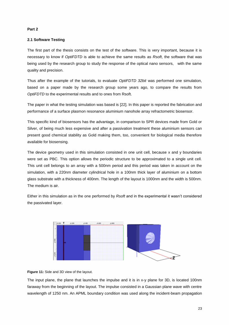
Figure 11: Side and 3D view of the layout............................................................................................. 23
Figure 12: Simulated transmission spectrum of an aluminium nanohole array calculated by OptiFDTD
32bit. ...................................................................................................................................................... 24
Figure 13: Rsoft Simulated transmission spectrum and experimental transmission spectrum of an
aluminium nanohole array. .................................................................................................................... 24
Figure 14: Layout of the device composed by a nanopillar array with a pitch of 600nm, the columns
have a diameter of 300nm and a height of 400nm. The array is supported by an aluminium layer with a
thickness of 100nm. ............................................................................................................................... 26
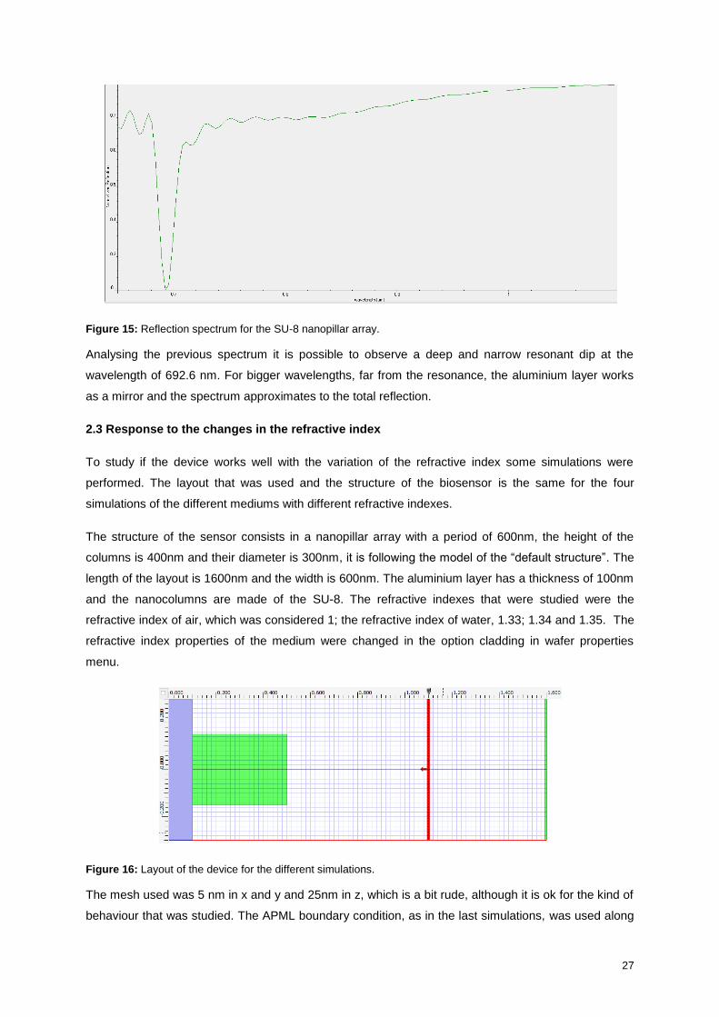
Figure 15: Reflection spectrum for the SU-8 nanopillar array. .............................................................. 27
Figure 16: Layout of the device for the different simulations. ................................................................ 27
Figure 17: Reflectivity profiles for the four different refractive indexes. In green air, in red water, in blue
1.34 and in yellow 1.35. ......................................................................................................................... 28
Figure 18: Position of the resonance dips versus the refractive index, with the equation of the linear
regression. ............................................................................................................................................. 29
Figure 19: Layout of the sensor with a gold layer. ................................................................................ 30
Figure 20: Spectrum for the biosensor with a gold layer instead of the aluminium layer. ..................... 30
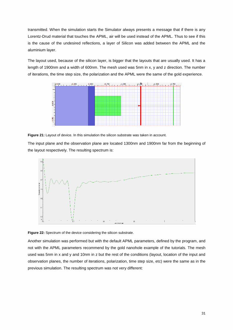
Figure 21: Layout of device. In this simulation the silicon substrate was taken in account. ................. 31
Figure 22: Spectrum of the device considering the silicon substrate. ................................................... 31
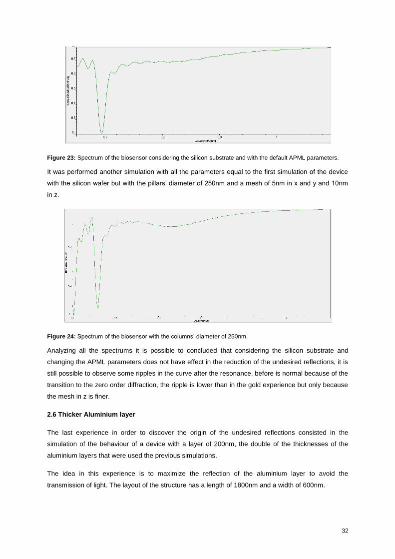
Figure 23: Spectrum of the biosensor considering the silicon substrate and with the default APML
parameters. ........................................................................................................................................... 32
Figure 24: Spectrum of the biosensor with the columns’ diameter of 250nm. ...................................... 32
Figure 25: Layout of the device that has an aluminium layer with the double of the thickness. ........... 33
Figure 26: Spectrum of the device with a layer of aluminium of 200nm. .............................................. 33
Figure 27: Layout of the biosensor structure with the y-z observation plane. ....................................... 35
6
Figure 28: Field distributions at wavelength of 692.6 nm. a) Ez field distribution in V/m. b) Hx field
distribution A/m. The black lines are structural outlines that were drawn to help the analysis of the field
distribution. Regarding the colours, red is for the highest amplitude and blue for the lowest. .............. 35
Figure 29: Fields distribution at the wavelength 1100nm, far from the resonance. a) Ez field distribution
in V/m. b) Hx field distribution in A/m. ................................................................................................... 36
Figure 30: Ez resonant field distribution in V/m for the device with a nopillars’ diameter of 200nm and a
height of 400nm. The period of the array is 600nm. ............................................................................. 36
Figure 31: Reflection spectrum for the device with a nanopillar array with a period of 600nm, with the
columns with a height of 400nm and a diameter of 100nm. .................................................................. 37
Figure 32: Sensitivities for the different pillars’ heights. ........................................................................ 38
Figure 33: FOM for the different pillar’s heights. ................................................................................... 38
Figure 34: FOM for the different pillars’ heights, considering the biolayer. ........................................... 39
Figure 35: Dip magnitude for the different pillars’ heights. .................................................................... 39
Figure 36: Dip magnitude for the different pillars’s heights, considering the biolayer. .......................... 40
Figure 37: Comparison of the sensitivities of the devices with the same pillars’ height but with a
different array period. ............................................................................................................................ 40
Figure 38: Comparison of the FOMs of the devices with the same pillars’ height but with a different
array period. .......................................................................................................................................... 40
Figure 39: Comparison of the FOMs of the devices with the same pillars’ height but with a different
array period, considering the biolayer. .................................................................................................. 41
Figure 40: Comparison of the dip magnitude of the devices with the same pillars’ height but with a
different array period. ............................................................................................................................ 41
Figure 41: Comparison of the FOMs of the devices with the same pillars’ height but with a different
array period, considering the biolayer. .................................................................................................. 41
Figure 42: Proximity effect, exposure at pixel A affects pixel B [27]. .................................................... 42
Figure 43: The different phenomena present in the e-beam lithography, the forward scattering, the
backscattering and the secondary electrons [3]. ................................................................................... 43
Figure 44: SEM side image of the biosensor where is possible to observe the consenquences of the
proximity effects. .................................................................................................................................... 44
Figure 45: Simulated reflection spectrum of a sensor with a 100nm thickness residual layer of SU-8. 44
Figure 46: a) Side view of the layout of the sensor structure. b) Distribution of the refractive indexes in
the x-z plane (in red bigger RI, and in blue zero). ................................................................................. 45
Figure 47: Layout of the sensor structure with the y-z observation plane. ............................................ 45
Figure 48: Ey field distribution for the first resonance dip in V/m. The black lines are structural outlines
that were drawn to help the analysis of the field distribution. Regarding the colours, red is for the
highest amplitude and blue for the lowest. ............................................................................................ 46
Figure 49: Fields distribution for the second resonance dip. a) Ez distribution in V/m. b) Ez distribution
in decibels. c) Hx distribution in A/m. .................................................................................................... 46
Figure 50: Distribution of the electromagnetic fields far from the resonance dips, at the wavelength
1100nm. a) Ey in decibels. b) Hx in A/m. .............................................................................................. 47

7
Figure 51: Reflection spectrum for the biosensor with a residual SU-8 layer with a thickness of 50nm.
............................................................................................................................................................... 47
Figure 52: Spectra of the devices with a thickness of 100nm and 50nm. In red and green the
spectrums of the biosensor with a residual layer of SU-8 with a thickness of 100nm and 50nm
respectively. ........................................................................................................................................... 48
Figure 53: Reflection spectrum for the biosensor with a residual SU-8 layer with a thickness of 150nm.
............................................................................................................................................................... 48
Figure 54: Spectra of the devices with a thickness of 100nm and 150nm. In red and green the
spectrums of the biosensor with a residual layer of SU-8 with a thickness of 100nm and 150nm
respectively. ........................................................................................................................................... 49
List of tables:
Table 1: Common types of biosensors with their classification based on their transduction mechanism,
in the red box the two types of biosensors that are studied in this thesis
[1].............................................................................................................................................................9
List of abbreviations:
E-beam Electron beam
ELISA Enzyme-linked Immunosorbent Assay
FDTD Finite-Difference Time Domain
FOM Figure of Merit
GMR Guided Mode Resonance
INESC Instituto de Engenharia e Sistemas de Computadores
MaGMR Metal Assisted Guided Mode Resonance
MTJ Magnetic Tunnel Junctions
SEM Scanning Electron Microscopy
SPP Surface Plasmon Polaritons
SPR Surface Plasmon Resonance
RIU Refractive Index Unit
8
Part 1
1.1 Introduction
This thesis is about the design and study of a surface plasmon resonance (SPR) biosensor. Being a
SPR device, the device studied here is label-free which offers many advantages, especially if the goal
is to study the target biomolecules in their natural state. The biosensor that is being studied consists in
a SU-8 resist nanopillar array above a layer of aluminium. To simulate the behaviour of the device it
was tested and used a free finite-difference time-domain (FDTD) software, OptiFDTD 32bit.
The present thesis is divided in two parts, the first part is the theoretical part where is given the
definition of biosensor and some types of biosensors are presented. It is also explained what is a
label-free biosensor and what are the advantages of this kind of devices. In order to the reader
understand the optical phenomena involved in the sensing of this sensor, a simple explanation of that
effects (surface plasmon resonance, surface plasmon polaritons, metal assisted guided mode
resonance) is provided. To understand the operation of OptiFDTD 32bit it is explained, too, how the
FDTD algorithm works. Finally there is a section concerned to the aluminium and to the SU-8 resist,
where the advantages of the use of these materials are described.
The second part concerns all the simulations performed in this master thesis, the software testing and
the pursuit for the design with the best performance.
A biosensor is an analytical device that is used for the detection of different kind of analytes. It
consists in a bioreceptor, which could be a biomolecule or a cell, for example, combined with a
physical or physiochemical transduction mechanism.
The number of applications for biosensors is increasing, which leads to a greater standardization of
the equipment, test processes and kinds of biomolecules. There are many areas where these devices
could be applied, the most common areas of application are Home Diagnostics, Environmental
Monitoring, Point of Care Testing, food industry, agriculture and Security.
The principal criteria for the evaluation of the performance of the biosensors are sensitivity, selectivity,
detection limits, operational and linear concentration range, reproducibility and stability. Other criteria
that should be taken in account are the cost of test, if the biosensors are easy to use or not, and the
time of analysis which includes not only the test part but it also includes all the steps needed for
sample preparation [1].
The final goal of the engineers that work with this kind of technology is to obtain a commercial and
competitive device. A great area of interest nowadays is the area of lab-on-chip devices that have the
possibility of multi-analyte detection, where the analytes are detected by the nano-sensors and the
signal is treated and processed by CMOS technology. All of these processes occurring in a reduced
area [2].
9
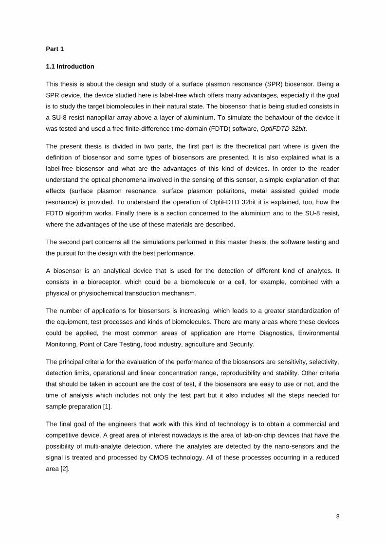
Usually the biosensors are classified by their transduction mode. The most common types are
represented in the following table:
Table 1: Common types of biosensors with their classification based on their transduction mechanism, in the red
box the two types of biosensors that are studied in this thesis [1].
There are many other kinds of biosensors, like the magnetic sensors in which are included the
magnetic tunnel junctions (MTJs) and the spin valves. Some successful results were obtained with this
kind of devices in INESC (Instituto de Engenharia de Sistemas e Computadores), Universidade de
Lisboa [3].
The electrochemical sensors are able to provide a direct conversion of one biological recognition
event into an electronic signal. These devices are based on bioelectrochemical receptor that serves as
the transduction element, in the bio-reaction of interested is possible to measure the current
(amperometric sensors, current vs concentration of the analyte), the potential (potentiometric sensors,
voltage vs concentration of the analyte) or is possible to measure a change in the conductive
properties of the medium (conductometric sensors).
The piezoelectric sensors are very useful to measure changes in pressure strain or force by
converting them to an electrical charge. This process of conversion is based on the piezoelectric
effect. With the use of piezoelectric crystals with their surface coated with biological recognition
elements, the biding of the target analytes to the receptors will produce a change in the applied force.
This change is measure by the change in the capacitance or the change in the voltage [5, 4].
If an alternating voltage is applied to the piezoelectric crystal, producing a standing wave with a
characteristic frequency, it is possible to measure the biding of the analytes to the receptors by the
change in the resonance frequency [1].
The optical biosensors are based on the detection of changes in properties of light which result from
the biding of the analyte to the surface of the sensor.
10
There many types of optical biosensors like the devices based on Fluorescent labelling, Enzyme-
linked Immunosorbent Assay (ELISA), Test strips, etc. This thesis is based on the ones that are label
free, especially on SPR biosensors.
Among the different kinds of sensor technologies, label-free biosensors, like the ones studied in this
thesis, offer many advantages because they can offer multi dimensional and highly sensitive
multiplexed detection, they are safe and non-invasive [1].
Labelling techniques allow the measure of signals from very small amounts of sample due to their
great power of amplification, for example thousands of dye molecules are activated for each target
analyte. Label free strategies are cheaper, they don’t need reporter elements so it isn’t necessary to
synthesize and purify the tracers. Label-based methods normally require two or more antibodies to the
target analyte while label-free techniques require only one [6].
For detailed studies of biomolecules in their natural state or close, label-free optical sensors, like the
devices studied in this thesis, are a better option because the labels can affect interactions [6].
The label-free techniques allow a real time analysis like the study of kinetics as will be explained
ahead [6].
The detection and quantification principle in label free optical biosensors is based on the measure of
the refractive index of the surrounding media which is modified by the presence of the biomolecules of
interest. The change of the surrounding medium, by the presence or absence of the target analytes
will cause a change in the refractive index of the medium [1].
1.2 SPP Theory
A plasmon is defined as the collective oscillation of the free electrons in a conductor, like a metal. It
can be seen as the mechanical oscillations of the electron cloud (the outer electrons are delocalized)
of the metal. The application of an external electric field will cause displacements of the electron cloud
with respect to the fixed ionic cores. The energy of the bulk plasmons is given by:
(1)
Where e is the electron charge, εo is the permittivity of the vacuum, n is the electron density and m is
the electron mass [6].
The Plasmon frequency, wp, for a bulk Plasma, where is the electric susceptibility, is given by the
following formula [7]:
11
(2)
When the light that is focusing on the plasma with a frequency below the plasma frequency, it will
induce motion in the charge carriers that will act to screen the incident radiation thus the incident
waves are reflected. Above the wp the free charges aren’t able to respond quickly enough to screen
out the incident field and the waves are instead transmitted. So this Plasmon frequency is very
important to characterize the optical properties of the materials. It is because of this phenomenon that
the metals reflect light in the visible region, which explains their historical use as mirrors [7].
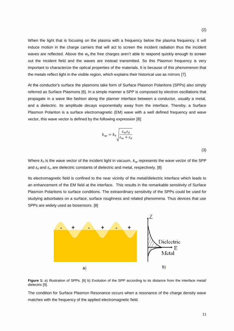
At the conductor’s surface the plasmons take form of Surface Plasmon Polaritons (SPPs) also simply
referred as Surface Plasmons [6]. In a simple manner a SPP is composed by electron oscillations that
propagate in a wave like fashion along the planner interface between a conductor, usually a metal,
and a dielectric. Its amplitude decays exponentially away from the interface. Thereby, a Surface
Plasmon Polariton is a surface electromagnetic (EM) wave with a well defined frequency and wave
vector, this wave vector is defined by the following expression [8]:
(3)
Where k0 is the wave vector of the incident light in vacuum, ksp represents the wave vector of the SPP
and εd and εm are dielectric constants of dielectric and metal, respectively. [8]
Its electromagnetic field is confined to the near vicinity of the metal/dielectric interface which leads to
an enhancement of the EM field at the interface. This results in the remarkable sensitivity of Surface
Plasmon Polaritons to surface conditions. The extraordinary sensitivity of the SPPs could be used for
studying adsorbates on a surface, surface roughness and related phenomena. Thus devices that use
SPPs are widely used as biosensors. [8]
Figure 1: a) Illustration of SPPs. [6] b) Evolution of the SPP according to its distance from the interface metal/
dielectric [9].
The condition for Surface Plasmon Resonance occurs when a resonance of the charge density wave
matches with the frequency of the applied electromagnetic field.
12
Analyzing the equation 3, it is possible to conclude that it is impossible the direct conversion from
propagation EM waves into SPPs. This impossibility is due to the mismatch of their wave vectors. To
solve this problem some coupling configurations could be adopted, the most used are the
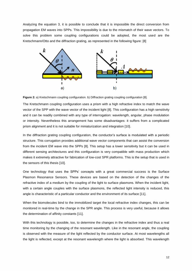
Kretschmann/Otto and the diffraction grating, as represented in the following figure: [8]
Figure 2: a) Kretschmann coupling configuration. b) Diffraction grating coupling configuration [8].
The Kretschmann coupling configuration uses a prism with a high refractive index to match the wave
vector of the SPP with the wave vector of the incident light [8]. This configuration has a high sensitivity
and it can be readily combined with any type of interrogation: wavelength, angular, phase modulation
or intensity. Nevertheless this arrangement has some disadvantages: it suffers from a complicated
prism alignment and it is not suitable for miniaturization and integration [10].
In the diffraction grating coupling configuration, the conductor’s surface is modulated with a periodic
structure. This corrugation provides additional wave vector components that can assist the conversion
from the incident EM wave into the SPPs [8]. This setup has a lower sensitivity but it can be used in
different sensing architectures and this configuration is very compatible with mass production which
makes it extremely attractive for fabrication of low-cost SPR platforms. This is the setup that is used in
the sensors of this thesis [10].
One technology that uses the SPPs’ concepts with a great commercial success is the Surface
Plasmon Resonance Sensors. These devices are based on the detection of the changes of the
refractive index of a medium by the coupling of the light to surface plasmons. When the incident light,
with a certain angle couples with the surface plasmons, the reflected light intensity is reduced, this
angle is characteristic of a particular conductor and the environment of its surface [11].
When the biomolecules bind to the immobilized target the local refractive index changes, this can be
monitored in real-time by the change in the SPR angle. This process is very useful, because it allows
the determination of affinity constants [11].
With this technology is possible, too, to determine the changes in the refractive index and thus a real
time monitoring by the changing of the resonant wavelength. Like in the resonant angle, the coupling
is observed with the measure of the light reflected by the conductor surface. At most wavelengths all
the light is reflected, except at the resonant wavelength where the light is absorbed. This wavelength
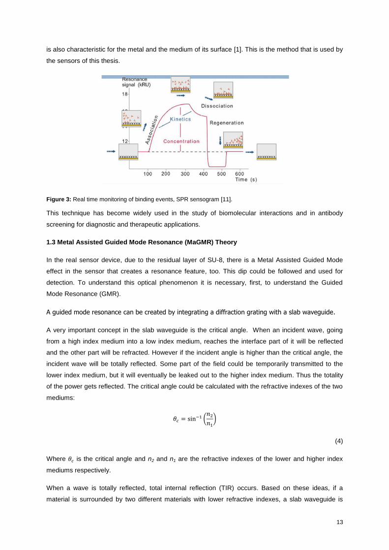
13
is also characteristic for the metal and the medium of its surface [1]. This is the method that is used by
the sensors of this thesis.
Figure 3: Real time monitoring of binding events, SPR sensogram [11].
This technique has become widely used in the study of biomolecular interactions and in antibody
screening for diagnostic and therapeutic applications.
1.3 Metal Assisted Guided Mode Resonance (MaGMR) Theory
In the real sensor device, due to the residual layer of SU-8, there is a Metal Assisted Guided Mode
effect in the sensor that creates a resonance feature, too. This dip could be followed and used for
detection. To understand this optical phenomenon it is necessary, first, to understand the Guided
Mode Resonance (GMR).
A guided mode resonance can be created by integrating a diffraction grating with a slab waveguide.
A very important concept in the slab waveguide is the critical angle. When an incident wave, going
from a high index medium into a low index medium, reaches the interface part of it will be reflected
and the other part will be refracted. However if the incident angle is higher than the critical angle, the
incident wave will be totally reflected. Some part of the field could be temporarily transmitted to the
lower index medium, but it will eventually be leaked out to the higher index medium. Thus the totality
of the power gets reflected. The critical angle could be calculated with the refractive indexes of the two
mediums:
(4)
Where is the critical angle and n2 and n1 are the refractive indexes of the lower and higher index
mediums respectively.
When a wave is totally reflected, total internal reflection (TIR) occurs. Based on these ideas, if a
material is surrounded by two different materials with lower refractive indexes, a slab waveguide is
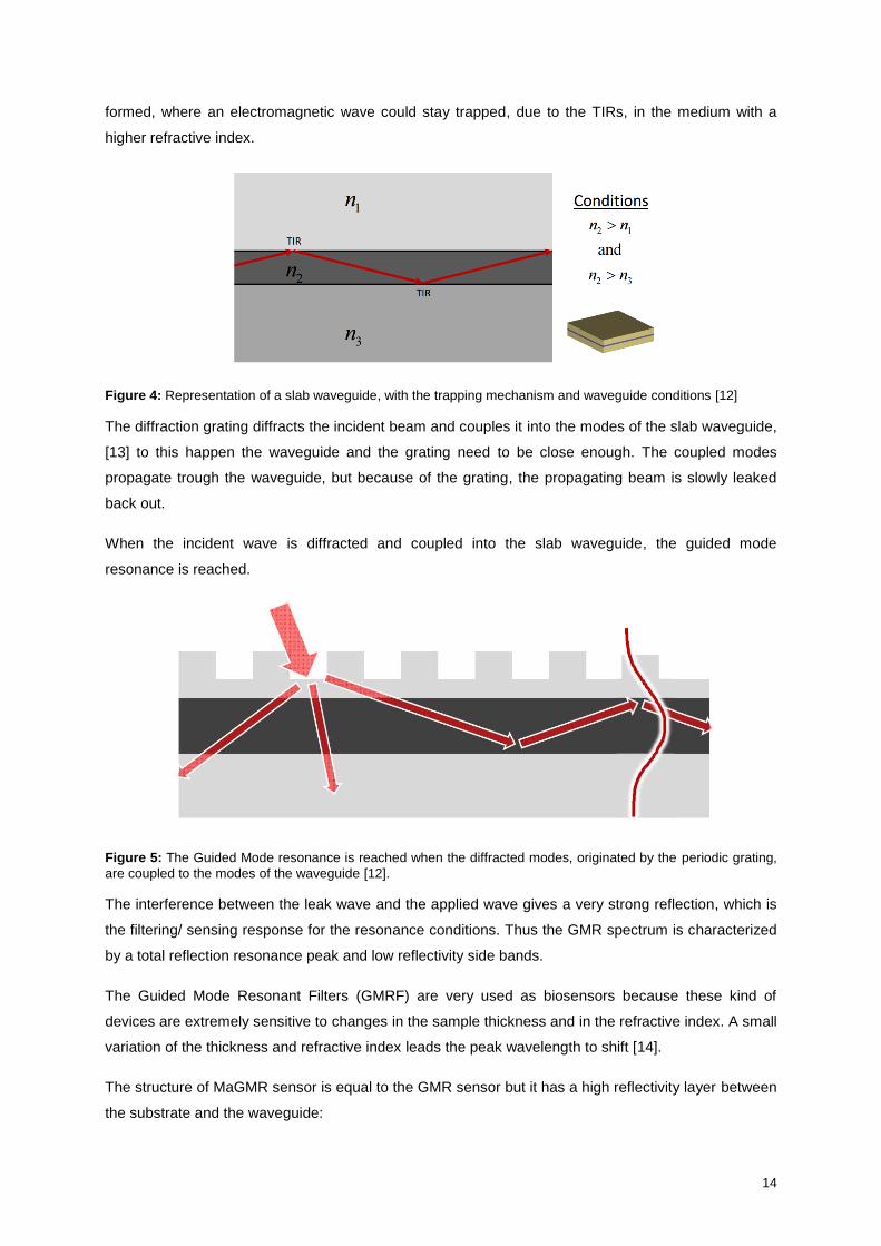
14
formed, where an electromagnetic wave could stay trapped, due to the TIRs, in the medium with a
higher refractive index.
Figure 4: Representation of a slab waveguide, with the trapping mechanism and waveguide conditions [12]
The diffraction grating diffracts the incident beam and couples it into the modes of the slab waveguide,
[13] to this happen the waveguide and the grating need to be close enough. The coupled modes
propagate trough the waveguide, but because of the grating, the propagating beam is slowly leaked
back out.
When the incident wave is diffracted and coupled into the slab waveguide, the guided mode
resonance is reached.
Figure 5: The Guided Mode resonance is reached when the diffracted modes, originated by the periodic grating,
are coupled to the modes of the waveguide [12].
The interference between the leak wave and the applied wave gives a very strong reflection, which is
the filtering/ sensing response for the resonance conditions. Thus the GMR spectrum is characterized
by a total reflection resonance peak and low reflectivity side bands.
The Guided Mode Resonant Filters (GMRF) are very used as biosensors because these kind of
devices are extremely sensitive to changes in the sample thickness and in the refractive index. A small
variation of the thickness and refractive index leads the peak wavelength to shift [14].
The structure of MaGMR sensor is equal to the GMR sensor but it has a high reflectivity layer between
the substrate and the waveguide:
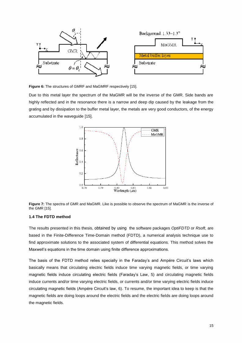
15
Figure 6: The structures of GMRF and MaGMRF respectively [15].
Due to this metal layer the spectrum of the MaGMR will be the inverse of the GMR. Side bands are
highly reflected and in the resonance there is a narrow and deep dip caused by the leakage from the
grating and by dissipation to the buffer metal layer, the metals are very good conductors, of the energy
accumulated in the waveguide [15].
Figure 7: The spectra of GMR and MaGMR. Like is possible to observe the spectrum of MaGMR is the inverse of
the GMR [15].
1.4 The FDTD method
The results presented in this thesis, obtained by using the software packages OptiFDTD or Rsoft, are
based in the Finite-Difference Time-Domain method (FDTD), a numerical analysis technique use to
find approximate solutions to the associated system of differential equations. This method solves the
Maxwell’s equations in the time domain using finite difference approximations.
The basis of the FDTD method relies specially in the Faraday’s and Ampére Circuit’s laws which
basically means that circulating electric fields induce time varying magnetic fields, or time varying
magnetic fields induce circulating electric fields (Faraday’s Law, 5) and circulating magnetic fields
induce currents and/or time varying electric fields, or currents and/or time varying electric fields induce
circulating magnetic fields (Ampére Circuit’s law, 6). To resume, the important idea to keep is that the
magnetic fields are doing loops around the electric fields and the electric fields are doing loops around
the magnetic fields.
16
(5)
(6)
Due to these two laws, the change in the Electric Field in time is dependent on the change Magnetic
field across the space, the curl. The Magnetic field behaves in a similar way. This is the basis of time
stepping in FDTD in which at any point in space the updated value of the Electric Field in time is
dependent on the stored value of the Electric Field and on the numerical curl the local distribution of
the Magnetic Field in space. In relation to the Magnetic field the process is similar, at any point in
space, the updated value of the Magnetic Field in time is dependent on the stored value of Magnetic
Field and on the numerical curl of the local distribution of the Electric Field in space. Thus the Electric
is updated from the magnetic field by calculating the curl of the Magnetic Field and by adding to the
current value of the Electric Field and then the Magnetic Field is updated based on the curl of the
Electric Field, this will go back and forward, the E is updated from H, and H is updated from E, this
cycle is repeated until the limit of iterations is reached [17].
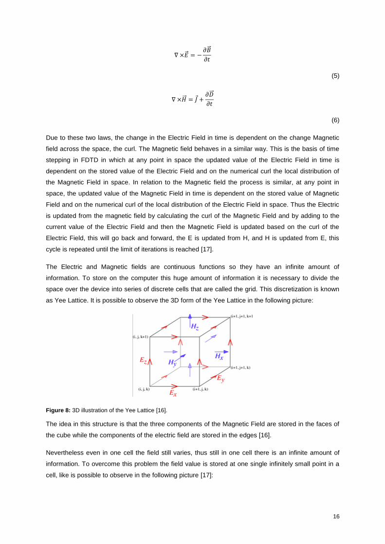
The Electric and Magnetic fields are continuous functions so they have an infinite amount of
information. To store on the computer this huge amount of information it is necessary to divide the
space over the device into series of discrete cells that are called the grid. This discretization is known
as Yee Lattice. It is possible to observe the 3D form of the Yee Lattice in the following picture:
Figure 8: 3D illustration of the Yee Lattice [16].
The idea in this structure is that the three components of the Magnetic Field are stored in the faces of
the cube while the components of the electric field are stored in the edges [16].
Nevertheless even in one cell the field still varies, thus still in one cell there is an infinite amount of
information. To overcome this problem the field value is stored at one single infinitely small point in a
cell, like is possible to observe in the following picture [17]:
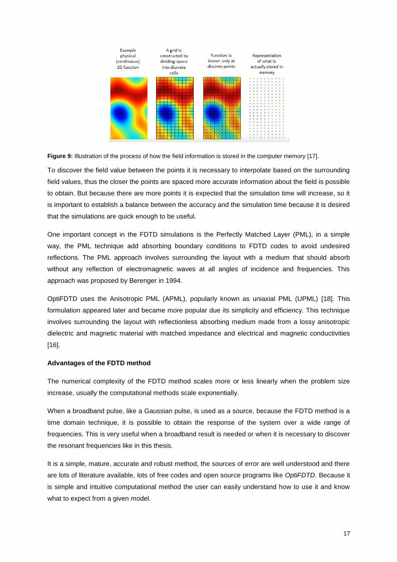
17
Figure 9: Illustration of the process of how the field information is stored in the computer memory [17].
To discover the field value between the points it is necessary to interpolate based on the surrounding
field values, thus the closer the points are spaced more accurate information about the field is possible
to obtain. But because there are more points it is expected that the simulation time will increase, so it
is important to establish a balance between the accuracy and the simulation time because it is desired
that the simulations are quick enough to be useful.
One important concept in the FDTD simulations is the Perfectly Matched Layer (PML), in a simple
way, the PML technique add absorbing boundary conditions to FDTD codes to avoid undesired
reflections. The PML approach involves surrounding the layout with a medium that should absorb
without any reflection of electromagnetic waves at all angles of incidence and frequencies. This
approach was proposed by Berenger in 1994.
OptiFDTD uses the Anisotropic PML (APML), popularly known as uniaxial PML (UPML) [18]. This
formulation appeared later and became more popular due its simplicity and efficiency. This technique
involves surrounding the layout with reflectionless absorbing medium made from a lossy anisotropic
dielectric and magnetic material with matched impedance and electrical and magnetic conductivities
[16].
Advantages of the FDTD method
The numerical complexity of the FDTD method scales more or less linearly when the problem size
increase, usually the computational methods scale exponentially.
When a broadband pulse, like a Gaussian pulse, is used as a source, because the FDTD method is a
time domain technique, it is possible to obtain the response of the system over a wide range of
frequencies. This is very useful when a broadband result is needed or when it is necessary to discover
the resonant frequencies like in this thesis.
It is a simple, mature, accurate and robust method, the sources of error are well understood and there
are lots of literature available, lots of free codes and open source programs like OptiFDTD. Because it
is simple and intuitive computational method the user can easily understand how to use it and know
what to expect from a given model.
18
In the FDTD method is possible to the user to specify the material at all points inside the
computational domain. A large diversity of nonlinear and linear, magnetic and dielectric materials can
be easily modelled.
Direct calculation of Maxwell’s equations everywhere in the computational domain as they evolve in
time, results in the possibility to provide field animations through the model which is very useful to
understand what is going on the device and if it is working correctly.
Drawbacks of FDTD
Usually the FDTD method is implemented on a structured Cartesian grid which is not efficient for
curved surfaces.
Since it is needed that the entire computational domain be gridded, in the FDTD modelling and to
resolve both the smallest geometrical feature and the smallest electromagnetic wavelength in the
model the grid spatial discretization should be sufficiently fine. This creates very large computational
domains which results in very long simulation times. Thus FDTD is a slow method for small devices or
devices with long and thin features like wires.
In the case of the Far Field analysis, where the electromagnetic field values at some distance are
desired, it is expected that this distance will enlarge excessively the computational domain. These
kinds of analysis are available for FDTD but require a longer simulation time and some amount of post
processing [17].
1.5 OptiFDTD 32bit
OptiFDTD is the software that is being used in this master thesis to study the response of the optical
nano sensors. This program is based on the FDTD technique which enables the users to design,
analyze and test modern passive and nonlinear photonic components, like optic nano sensors, golden
nano particles, for wave propagation, transmission, reflection, polarization, scattering and the study of
surface plasmons [19].
OptiFDTD is provided by Optiwave Systems Inc. This company provides optical component and
system design tools for high-technology businesses. It is based in Ottawa in Canada and was founded
in 1994. Optiwave offers its products through a network of distributors in the American continent, Asia
and Europe. Besides OptiFDTD, Optiwave Systems also provides other softwares like OptiSPICE,
OptiSystem, OptiBPM, OptiFiber and OptiGrating[19].
In this thesis is being used the free version of FDTD, the 32 bit version. This is user friendly software,
very easy to learn how to use it and it displays a library with a large diversity of materials, which is very
useful because it is simple in OptiFDTD to define the material parameters. Optiwave also provides a
forum in their website where the OptiFDTD users can clarify doubts with each others.
The entire package of OptiFDTD could be divided in four main applications [20]:

19
1. Layout Designer, here is where the structure and the simulation conditions are defined.
2. Profile Designer, here is where the materials and the profiles used in the simulation are
defined.
3. Simulator, it is started from the layout designer, loads the designer file and performs the
simulation.
4. Analyzer, this application is used to view the results and it performs some post processing.
Even though OptiFDTD 32 bit is an open source software, easy to use and very intuitive, it has some
drawbacks:
The 32Bit OptiFDTD simulations can only use maximum 2GB of RAM which means that for a 3D
simulation, the ones that are performed in this thesis, the maximum number of grid cells that can be
handled will be more or less 300x300x300. These simulations only support a single core processor.
In OptiFDTD 32bit isn’t available the option Non Uniform Mesh in the Simulator, with this option could
be possible to define a finer grid in the interface, where is it more important and desired, and a ruder
mesh far from the interfaces, where the precision is not important. This combined with the limit in RAM
and in the fact that OptiFDTD 32bit only use a single core in the processor makes the simulations very
slow. Almost all of the each simulation realised in this thesis took a day to finish and one of them took
2days [20, 21].
1.6 Aluminium
Aluminium is a chemical element with an atomic number 13 and the symbol Al. Aluminium is the most
abundant metal in the Earth’s crust and it is a plasmonic material as gold and silver. Aluminium is
remarkable for its resistance against corrosion after a passivation treatment. This treatment involves
the oxidation of the aluminium surface that is exposed to air, transforming this contact surface into
thin, insulating, water insoluble and waterproof film which is resistant to reactions with oxygen, water
or diluted acids. This oxide thin film protects the inner aluminium and prevents further oxidation.
Nowadays the majority of SPR devices are made of gold or silver [30, 31] due to their low resistivity.
Comparatively to silver, gold has a much higher chemical stability, making this material much more
convenient for biological environments than silver. The poorer environmental stability of silver can be
solved by the deposition of an over layer of alumina via atomic layer deposition.
Nevertheless gold and silver have a high cost which limits the large-scale commercialization of
sensors made with these metals. Comparatively to theses metals, aluminium is ~425 times cheaper
than silver and ~25 000 times cheaper than gold [22, 32].
Aluminium is barely considered for the implementation of SPR biosensors due to the challenges from
oxidation and material degradation [33-35], however due some successful passivation techniques as
the one described in [22], aluminium could be used in SPR biosensors, like the ones of this thesis,
20
making them very cost competitive and enabling the large-scale commercialization of these SPR
devices.
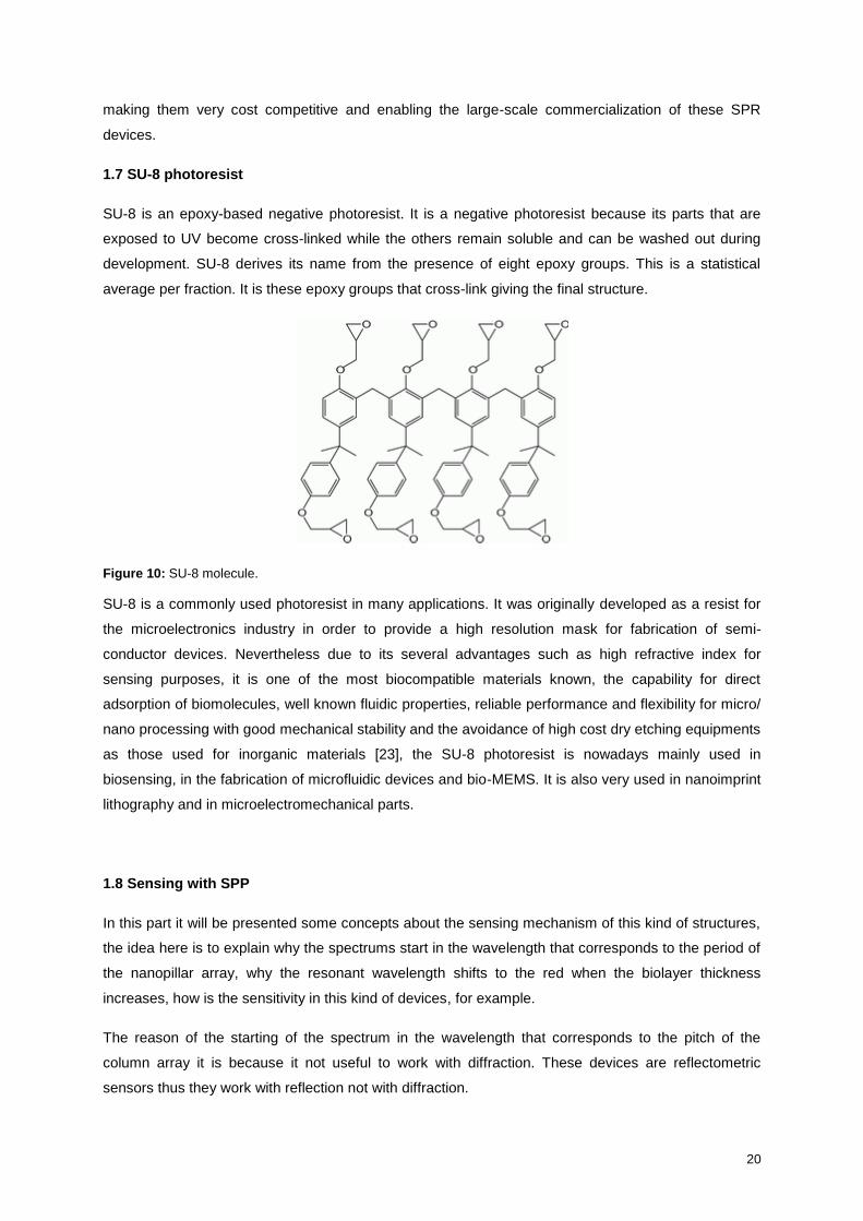
1.7 SU-8 photoresist
SU-8 is an epoxy-based negative photoresist. It is a negative photoresist because its parts that are
exposed to UV become cross-linked while the others remain soluble and can be washed out during
development. SU-8 derives its name from the presence of eight epoxy groups. This is a statistical
average per fraction. It is these epoxy groups that cross-link giving the final structure.
Figure 10: SU-8 molecule.
SU-8 is a commonly used photoresist in many applications. It was originally developed as a resist for
the microelectronics industry in order to provide a high resolution mask for fabrication of semi-
conductor devices. Nevertheless due to its several advantages such as high refractive index for
sensing purposes, it is one of the most biocompatible materials known, the capability for direct
adsorption of biomolecules, well known fluidic properties, reliable performance and flexibility for micro/
nano processing with good mechanical stability and the avoidance of high cost dry etching equipments
as those used for inorganic materials [23], the SU-8 photoresist is nowadays mainly used in
biosensing, in the fabrication of microfluidic devices and bio-MEMS. It is also very used in nanoimprint
lithography and in microelectromechanical parts.
1.8 Sensing with SPP
In this part it will be presented some concepts about the sensing mechanism of this kind of structures,
the idea here is to explain why the spectrums start in the wavelength that corresponds to the period of
the nanopillar array, why the resonant wavelength shifts to the red when the biolayer thickness
increases, how is the sensitivity in this kind of devices, for example.
The reason of the starting of the spectrum in the wavelength that corresponds to the pitch of the
column array it is because it not useful to work with diffraction. These devices are reflectometric
sensors thus they work with reflection not with diffraction.

21
For these devices to work in the reflection they need to be, therefore, in the zero order mode. In the
zero order mode, m=0, the light beam behaves according to the laws of refraction and reflection the
same as a lens or a mirror respectively.
To know for which wavelengths the sensor is working in the zero order mode, it is necessary to
analyze the Bragg’s Law [17]:
(7)
Assuming normal incidence and that the medium is air, the equation becomes simpler:
(8)
Because it is not desired that the device works in the first order mode, m=1, but in the zero order
mode, the condition to prevent first order modes needs to be fulfilled:
(9)
Where λ is the resonant wavelength, the array period and m an integer that represents the
diffraction mode. This is the reason why it does not make sense to plot the wavelengths in the
spectrum inferior to the period of the nanopillar array.
The resonant wavelength is linearly proportional to the refractive index, as it is possible to observe in
the next part of the thesis. Therefore the sensitivity is given by [14]:
(10)
Where Sn is the sensitivity, n is the refractive index and the resonant wavelength.
In this thesis to study the performance of the sensors, the change in the refractive index is indirectly
measured by the change of the optical thickness. The optical thickness is given by the refractive
index n and the physical thickness d of the layer. Changes in this variable are caused by molecular
interactions at the interface receptor layer/solution of the device, when the ligands bind to the
receptors, the refractive index of the interface receptor/solution changes and physical thickness of the
interface increases [24].
Therefore in this thesis the simulations are focused on the measurement of the changes in the
physical thickness of the biolayer. The sensitivity for this type of measurements is given by [14]:

22
(11)
Where Sd is the sensitivity, d is physical thickness of the biolayer and the resonant wavelength. As
the thickness of the biolayer increases the resonant dip shifts to longer wavelengths, This happens
because the biolayer increases the optical thickness in the following resonance condition [17]:
(12)
Where m is an integer, n the refractive index, d is physical thickness of the biolayer and the
wavelength. Analysing this is expression it is possible to conclude that when the physical thickness of
the biolayer increases the resonant wavelength moves to the red.
The resonant dip shifts to longer wavelengths as the thickness increases until it reaches a constant
value. This happens because the SPP takes the form of an evanescent field that decays exponentially
in the z direction. Thus if the biolayer is too thick the SPP evanescent field cannot reach the top part of
the biolayer. This phenomenon, the resonant dip reaches a constant wavelength, can also happen if
the concentration of analytes is so high that there are no more receptors available. [23].
Because SPP sensing is based on spectral dip shifts, the precision that can be achieved with respect
to changes in the optical thickness depends on the sensitivity, Sd, and the dip line width. Some
structures could have high sensitivities but their dips could be also wide. Therefore it is important to
define a Figure of Merit, FOM, which is able to characterize in a global way, the precision of this kind
of devices [6]:
(13)
Where S is the sensitivity and at the dip half minimum.
23
Part 2
2.1 Software Testing
The first part of the thesis consists on the test of the software. This is very important, because it is
necessary to know if OptiFDTD is able to achieve the same results as Rsoft, the software that was
being used by the research group to study the response of the optical nano sensors, with the same
quality and precision.
Thus after the example of the tutorials, to evaluate OptiFDTD 32bit was performed one simulation,
based on a paper made by the research group some years ago, to compare the results from
OptiFDTD to the experimental results and to ones from Rsoft.
The paper in what the testing simulation was based is [22]. In this paper is reported the fabrication and
performance of a surface plasmon resonance aluminium nanohole array refractometric biosensor.
This specific kind of biosensors has the advantage, in comparison to SPR devices made from Gold or
Silver, of being much less expensive and after a passivation treatment these aluminium sensors can
present good chemical stability as Gold making them, too, convenient for biological media therefore
available for biosensing.
The device geometry used in this simulation consisted in one unit cell, because x and y boundaries
were set as PBC. This option allows the periodic structure to be approximated to a single unit cell.
This unit cell belongs to an array with a 500nm period and this period was taken in account on the
simulation, with a 220nm diameter cylindrical hole in a 100nm thick layer of aluminium on a bottom
glass substrate with a thickness of 400nm. The length of the layout is 1000nm and the width is 500nm.
The medium is air.
Either in this simulation as in the one performed by Rsoft and in the experimental it wasn’t considered
the passivated layer.
Figure 11: Side and 3D view of the layout.
The input plane, the plane that launches the impulse and it is in x-y plane for 3D, is located 100nm
faraway from the beginning of the layout. The impulse consisted in a Gaussian plane wave with centre
wavelength of 1250 nm. An APML boundary condition was used along the incident-beam propagation
24
(z-axis), normal to the sensor plane. The mesh size used was 2nm in x and y and 10nm in z. The
number of iterations was 12000 and the time step size was defined by the program (automatic).
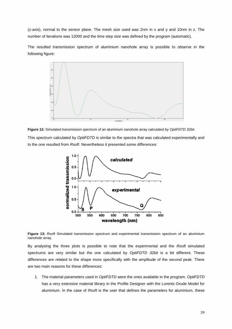
The resulted transmission spectrum of aluminium nanohole array is possible to observe in the
following figure:
Figure 12: Simulated transmission spectrum of an aluminium nanohole array calculated by OptiFDTD 32bit.
This spectrum calculated by OptiFDTD is similar to the spectra that was calculated experimentally and
to the one resulted from Rsoft. Nevertheless it presented some differences:
Figure 13: Rsoft Simulated transmission spectrum and experimental transmission spectrum of an aluminium
nanohole array.
By analysing the three plots is possible to note that the experimental and the Rsoft simulated
spectrums are very similar but the one calculated by OptiFDTD 32bit is a bit different. These
differences are related to the shape more specifically with the amplitude of the second peak. There
are two main reasons for these differences:
1. The material parameters used in OptiFDTD were the ones available in the program. OptiFDTD
has a very extensive material library in the Profile Designer with the Lorentz-Drude Model for
aluminium. In the case of Rsoft is the user that defines the parameters for aluminium, these
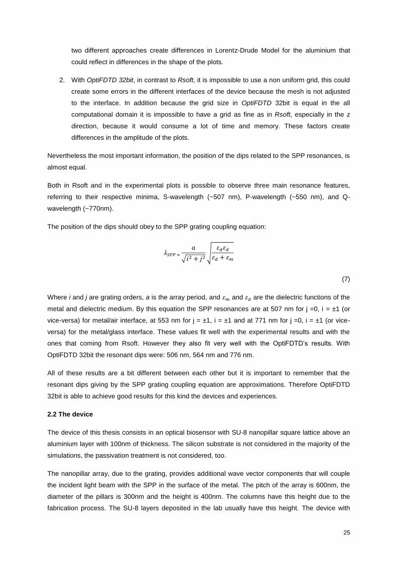
25
two different approaches create differences in Lorentz-Drude Model for the aluminium that
could reflect in differences in the shape of the plots.
2. With OptiFDTD 32bit, in contrast to Rsoft, it is impossible to use a non uniform grid, this could
create some errors in the different interfaces of the device because the mesh is not adjusted
to the interface. In addition because the grid size in OptiFDTD 32bit is equal in the all
computational domain it is impossible to have a grid as fine as in Rsoft, especially in the z
direction, because it would consume a lot of time and memory. These factors create
differences in the amplitude of the plots.
Nevertheless the most important information, the position of the dips related to the SPP resonances, is
almost equal.
Both in Rsoft and in the experimental plots is possible to observe three main resonance features,
referring to their respective minima, S-wavelength (~507 nm), P-wavelength (~550 nm), and Q-
wavelength (~770nm).
The position of the dips should obey to the SPP grating coupling equation:
(7)
Where i and j are grating orders, a is the array period, and and are the dielectric functions of the
metal and dielectric medium. By this equation the SPP resonances are at 507 nm for j =0, i = ±1 (or
vice-versa) for metal/air interface, at 553 nm for j = ±1, i = ±1 and at 771 nm for j =0, i = ±1 (or vice-
versa) for the metal/glass interface. These values fit well with the experimental results and with the
ones that coming from Rsoft. However they also fit very well with the OptiFDTD’s results. With
OptiFDTD 32bit the resonant dips were: 506 nm, 564 nm and 776 nm.
All of these results are a bit different between each other but it is important to remember that the
resonant dips giving by the SPP grating coupling equation are approximations. Therefore OptiFDTD
32bit is able to achieve good results for this kind the devices and experiences.
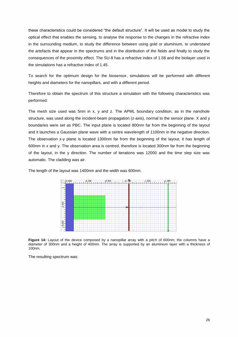
2.2 The device
The device of this thesis consists in an optical biosensor with SU-8 nanopillar square lattice above an
aluminium layer with 100nm of thickness. The silicon substrate is not considered in the majority of the
simulations, the passivation treatment is not considered, too.
The nanopillar array, due to the grating, provides additional wave vector components that will couple
the incident light beam with the SPP in the surface of the metal. The pitch of the array is 600nm, the
diameter of the pillars is 300nm and the height is 400nm. The columns have this height due to the
fabrication process. The SU-8 layers deposited in the lab usually have this height. The device with
26
these characteristics could be considered “the default structure”. It will be used as model to study the
optical effect that enables the sensing, to analyse the response to the changes in the refractive index
in the surrounding medium, to study the difference between using gold or aluminium, to understand
the artefacts that appear in the spectrums and in the distribution of the fields and finally to study the
consequences of the proximity effect. The SU-8 has a refractive index of 1.58 and the biolayer used in
the simulations has a refractive index of 1.45.
To search for the optimum design for the biosensor, simulations will be performed with different
heights and diameters for the nanopillars, and with a different period.
Therefore to obtain the spectrum of this structure a simulation with the following characteristics was
performed:
The mesh size used was 5nm in x, y and z. The APML boundary condition, as in the nanohole
structure, was used along the incident-beam propagation (z-axis), normal to the sensor plane. X and y
boundaries were set as PBC. The input plane is located 800nm far from the beginning of the layout
and it launches a Gaussian plane wave with a centre wavelength of 1100nm in the negative direction.
The observation x-y plane is located 1300nm far from the beginning of the layout, it has length of
600nm in x and y. The observation area is centred, therefore is located 300nm far from the beginning
of the layout, in the y direction. The number of iterations was 12000 and the time step size was
automatic. The cladding was air.
The length of the layout was 1400nm and the width was 600nm.
Figure 14: Layout of the device composed by a nanopillar array with a pitch of 600nm, the columns have a
diameter of 300nm and a height of 400nm. The array is supported by an aluminium layer with a thickness of 100nm.
The resulting spectrum was:
27
Figure 15: Reflection spectrum for the SU-8 nanopillar array.
Analysing the previous spectrum it is possible to observe a deep and narrow resonant dip at the
wavelength of 692.6 nm. For bigger wavelengths, far from the resonance, the aluminium layer works
as a mirror and the spectrum approximates to the total reflection.
2.3 Response to the changes in the refractive index
To study if the device works well with the variation of the refractive index some simulations were
performed. The layout that was used and the structure of the biosensor is the same for the four
simulations of the different mediums with different refractive indexes.
The structure of the sensor consists in a nanopillar array with a period of 600nm, the height of the
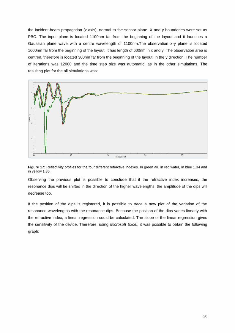
columns is 400nm and their diameter is 300nm, it is following the model of the “default structure”. The
length of the layout is 1600nm and the width is 600nm. The aluminium layer has a thickness of 100nm
and the nanocolumns are made of the SU-8. The refractive indexes that were studied were the
refractive index of air, which was considered 1; the refractive index of water, 1.33; 1.34 and 1.35. The
refractive index properties of the medium were changed in the option cladding in wafer properties
menu.
Figure 16: Layout of the device for the different simulations.
The mesh used was 5 nm in x and y and 25nm in z, which is a bit rude, although it is ok for the kind of
behaviour that was studied. The APML boundary condition, as in the last simulations, was used along
28
the incident-beam propagation (z-axis), normal to the sensor plane. X and y boundaries were set as
PBC. The input plane is located 1100nm far from the beginning of the layout and it launches a
Gaussian plane wave with a centre wavelength of 1100nm.The observation x-y plane is located
1600nm far from the beginning of the layout, it has length of 600nm in x and y. The observation area is
centred, therefore is located 300nm far from the beginning of the layout, in the y direction. The number
of iterations was 12000 and the time step size was automatic, as in the other simulations. The
resulting plot for the all simulations was:
Figure 17: Reflectivity profiles for the four different refractive indexes. In green air, in red water, in blue 1.34 and
in yellow 1.35.
Observing the previous plot is possible to conclude that if the refractive index increases, the
resonance dips will be shifted in the direction of the higher wavelengths, the amplitude of the dips will
decrease too.
If the position of the dips is registered, it is possible to trace a new plot of the variation of the
resonance wavelengths with the resonance dips. Because the position of the dips varies linearly with
the refractive index, a linear regression could be calculated. The slope of the linear regression gives
the sensitivity of the device. Therefore, using Microsoft Excel, it was possible to obtain the following
graph:
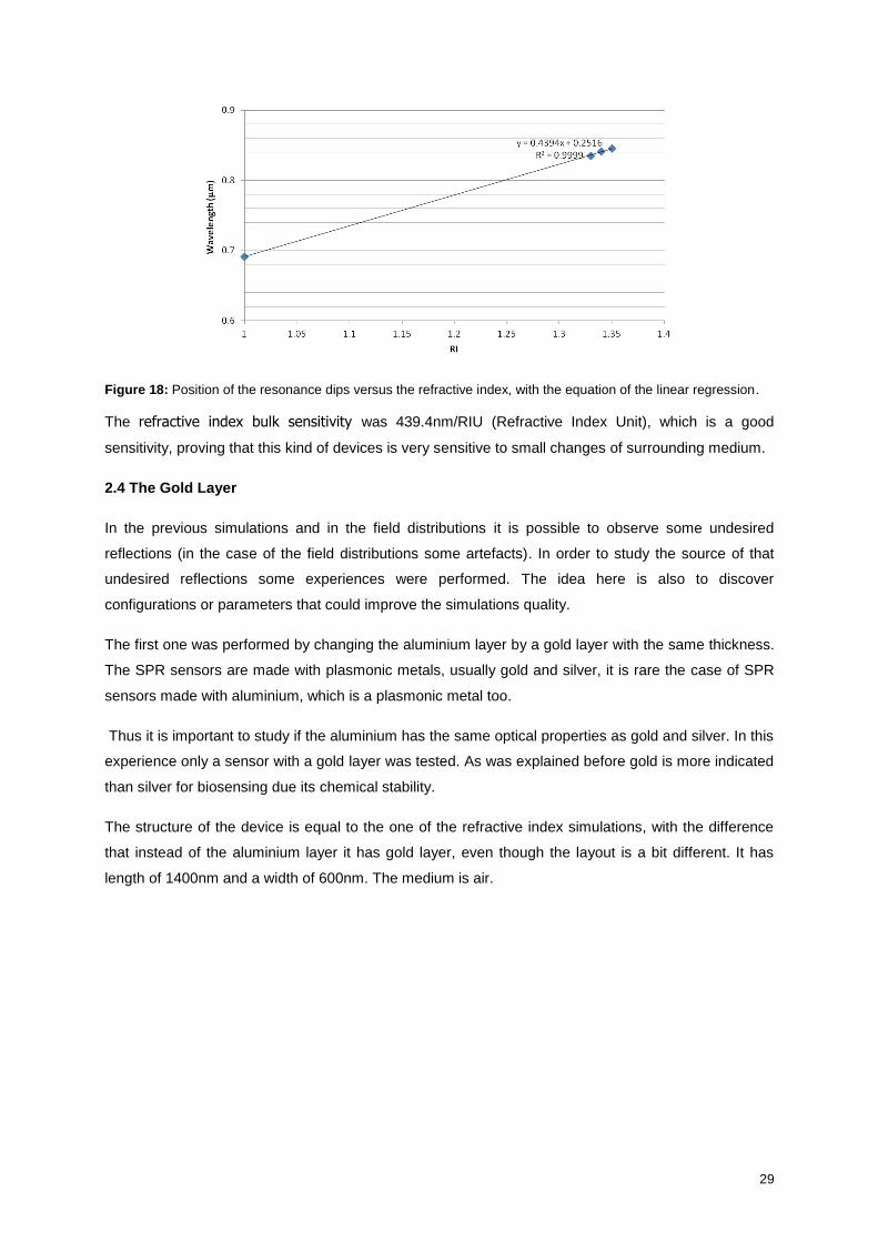
29
Figure 18: Position of the resonance dips versus the refractive index, with the equation of the linear regression.
The refractive index bulk sensitivity was 439.4nm/RIU (Refractive Index Unit), which is a good
sensitivity, proving that this kind of devices is very sensitive to small changes of surrounding medium.
2.4 The Gold Layer
In the previous simulations and in the field distributions it is possible to observe some undesired
reflections (in the case of the field distributions some artefacts). In order to study the source of that
undesired reflections some experiences were performed. The idea here is also to discover
configurations or parameters that could improve the simulations quality.
The first one was performed by changing the aluminium layer by a gold layer with the same thickness.
The SPR sensors are made with plasmonic metals, usually gold and silver, it is rare the case of SPR
sensors made with aluminium, which is a plasmonic metal too.
Thus it is important to study if the aluminium has the same optical properties as gold and silver. In this
experience only a sensor with a gold layer was tested. As was explained before gold is more indicated
than silver for biosensing due its chemical stability.
The structure of the device is equal to the one of the refractive index simulations, with the difference
that instead of the aluminium layer it has gold layer, even though the layout is a bit different. It has
length of 1400nm and a width of 600nm. The medium is air.
30
Figure 19: Layout of the sensor with a gold layer.
The mesh used is the same of the used in the refractive index experience, as the number of iterations
and the time step size. The APML boundary condition, as in the refractive index experience, was used
along the incident-beam propagation (z-axis), normal to the sensor plane. X and y boundaries were
set as PBC. The input plane is located 800nm far from the beginning of the layout and it launches a
Gaussian plane wave with a centre wavelength of 1100nm.The observation x-y plane is located
1300nm far from the beginning of the layout, it has length of 600nm in x and y. The observation area is
centred, therefore is located 300nm far from the beginning of the layout, in the y direction, the same of
the last simulations. The resulting spectrum was:
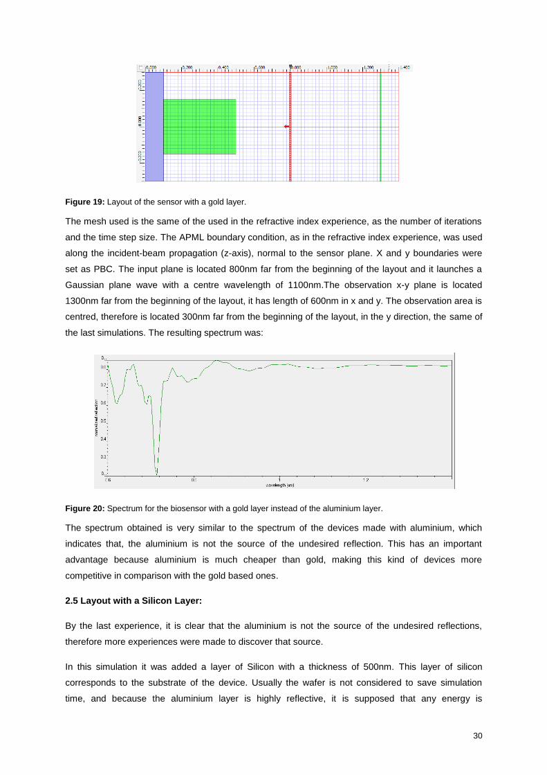
Figure 20: Spectrum for the biosensor with a gold layer instead of the aluminium layer.
The spectrum obtained is very similar to the spectrum of the devices made with aluminium, which
indicates that, the aluminium is not the source of the undesired reflection. This has an important
advantage because aluminium is much cheaper than gold, making this kind of devices more
competitive in comparison with the gold based ones.
2.5 Layout with a Silicon Layer:
By the last experience, it is clear that the aluminium is not the source of the undesired reflections,
therefore more experiences were made to discover that source.
In this simulation it was added a layer of Silicon with a thickness of 500nm. This layer of silicon
corresponds to the substrate of the device. Usually the wafer is not considered to save simulation
time, and because the aluminium layer is highly reflective, it is supposed that any energy is
31
transmitted. When the simulation starts the Simulator always presents a message that if there is any
Lorentz-Drud material that touches the APML, air will be used instead of the APML. Thus to see if this
is the cause of the undesired reflections, a layer of Silicon was added between the APML and the
aluminium layer.
The layout used, because of the silicon layer, is bigger that the layouts that are usually used. It has a
length of 1900nm and a width of 600nm. The mesh used was 5nm in x, y and z direction. The number
of iterations, the time step size, the polarization and the APML were the same of the gold experience.
Figure 21: Layout of device. In this simulation the silicon substrate was taken in account.
The input plane and the observation plane are located 1300nm and 1900nm far from the beginning of
the layout respectively. The resulting spectrum is:
Figure 22: Spectrum of the device considering the silicon substrate.
Another simulation was performed but with the default APML parameters, defined by the program, and
not with the APML parameters recommend by the gold nanohole example of the tutorials. The mesh
used was 5nm in x and y and 10nm in z but the rest of the conditions (layout, location of the input and
observation planes, the number of iterations, polarization, time step size, etc) were the same as in the
previous simulation. The resulting spectrum was not very different:
32
Figure 23: Spectrum of the biosensor considering the silicon substrate and with the default APML parameters.
It was performed another simulation with all the parameters equal to the first simulation of the device
with the silicon wafer but with the pillars’ diameter of 250nm and a mesh of 5nm in x and y and 10nm
in z.
Figure 24: Spectrum of the biosensor with the columns’ diameter of 250nm.
Analyzing all the spectrums it is possible to concluded that considering the silicon substrate and
changing the APML parameters does not have effect in the reduction of the undesired reflections, it is
still possible to observe some ripples in the curve after the resonance, before is normal because of the
transition to the zero order diffraction, the ripple is lower than in the gold experience but only because
the mesh in z is finer.
2.6 Thicker Aluminium layer
The last experience in order to discover the origin of the undesired reflections consisted in the
simulation of the behaviour of a device with a layer of 200nm, the double of the thicknesses of the
aluminium layers that were used the previous simulations.
The idea in this experience is to maximize the reflection of the aluminium layer to avoid the
transmission of light. The layout of the structure has a length of 1800nm and a width of 600nm.
33
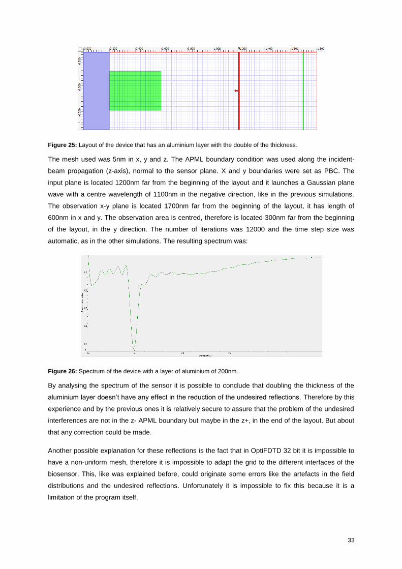
Figure 25: Layout of the device that has an aluminium layer with the double of the thickness.
The mesh used was 5nm in x, y and z. The APML boundary condition was used along the incident-
beam propagation (z-axis), normal to the sensor plane. X and y boundaries were set as PBC. The
input plane is located 1200nm far from the beginning of the layout and it launches a Gaussian plane
wave with a centre wavelength of 1100nm in the negative direction, like in the previous simulations.
The observation x-y plane is located 1700nm far from the beginning of the layout, it has length of
600nm in x and y. The observation area is centred, therefore is located 300nm far from the beginning
of the layout, in the y direction. The number of iterations was 12000 and the time step size was
automatic, as in the other simulations. The resulting spectrum was:
Figure 26: Spectrum of the device with a layer of aluminium of 200nm.
By analysing the spectrum of the sensor it is possible to conclude that doubling the thickness of the
aluminium layer doesn’t have any effect in the reduction of the undesired reflections. Therefore by this
experience and by the previous ones it is relatively secure to assure that the problem of the undesired
interferences are not in the z- APML boundary but maybe in the z+, in the end of the layout. But about
that any correction could be made.
Another possible explanation for these reflections is the fact that in OptiFDTD 32 bit it is impossible to
have a non-uniform mesh, therefore it is impossible to adapt the grid to the different interfaces of the
biosensor. This, like was explained before, could originate some errors like the artefacts in the field
distributions and the undesired reflections. Unfortunately it is impossible to fix this because it is a
limitation of the program itself.
34
2.7 Origin of the resonant dip
By the previous simulations it is possible to observe that this kind of biosensor is able to detect small
changes in the refractive index of the medium with a good sensitivity and it presents spectrums with
deep and narrow dips.
Furthermore it is important to confirm the optical phenomenon that originates these dips. By the theory
and by the structure of the device it is expect that the resonance is due to the SPP effect, nevertheless
it is important to confirm this guess.
Therefore it is necessary to analyze distribution of the fields. To obtain the different field distributions
another simulation was performed. In the new simulation a different observation area was defined in
order to get a distribution of the fields in the z direction. Because the incident plane is linearly
polarized in y and the wave is propagating in the z direction, the chosen plane for the observation area
was the y-z plane. It has a length in the z direction of 1400nm in order to cover the entire layout and a
length of 600nm in the y direction, for the same reason. The observation plane is centred in the layout,
thus at 300nm far from the beginning of the layout in the y direction. It was chosen to perform another
simulation instead of using the x-y and y-z observation planes in the same layout because the
analyzer files occupy a lot of memory, in the order of 5/7 GB per observation area, and they are
eliminated after getting the spectra. The analyzer file with the two observation areas would occupy
more or less 13GB. Because it is necessary to take different pictures of the different fields at different
wavelengths (in the resonance dips, far from the resonance), it is useful to maintain the analyzer file,
therefore is wise to do the simulations for the spectra and for the distributions of the electric field
separately.
Like in the previous simulations the nanopillar array has a pitch of 600nm, the height of the columns is
400nm and their diameter is 300nm. The length of the layout is 1400nm and the width is 600nm. The
medium is air.
The mesh size used was 5nm in x, y and z. The APML boundary condition was used along the
incident-beam propagation (z-axis), normal to the sensor plane. X and y boundaries were set as PBC.
The input plane is located 800nm far from the beginning of the layout and it launches a Gaussian
plane wave with a centre wavelength of 1100nm. The number of iterations was 12000 and the time
step size was automatic, as in the other simulations.
35
Figure 27: Layout of the biosensor structure with the y-z observation plane.
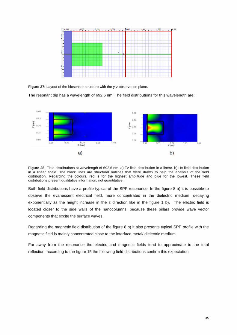
The resonant dip has a wavelength of 692.6 nm. The field distributions for this wavelength are:
Figure 28: Field distributions at wavelength of 692.6 nm. a) Ez field distribution in a linear. b) Hx field distribution
in a linear scale. The black lines are structural outlines that were drawn to help the analysis of the field distribution. Regarding the colours, red is for the highest amplitude and blue for the lowest. These field distributions present qualitative information, not quantitative.
Both field distributions have a profile typical of the SPP resonance. In the figure 8 a) it is possible to
observe the evanescent electrical field, more concentrated in the dielectric medium, decaying
exponentially as the height increase in the z direction like in the figure 1 b). The electric field is
located closer to the side walls of the nanocolumns, because these pillars provide wave vector
components that excite the surface waves.
Regarding the magnetic field distribution of the figure 8 b) it also presents typical SPP profile with the
magnetic field is mainly concentrated close to the interface metal/ dielectric medium.
Far away from the resonance the electric and magnetic fields tend to approximate to the total
reflection, according to the figure 15 the following field distributions confirm this expectation:
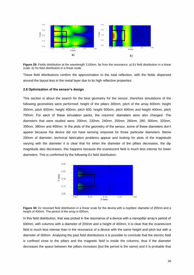
36
Figure 29: Fields distribution at the wavelength 1100nm, far from the resonance. a) Ez field distribution in a linear
scale. b) Hx field distribution in a linear scale.
These field distributions confirm the approximation to the total reflection, with the fields dispersed
around the layout less in the metal layer due to its high reflective properties.
2.8 Optimization of the sensor’s design
This section is about the search for the best geometry for the sensor, therefore simulations of the
following geometries were performed: height of the pillars 300nm, pitch of the array 600nm; height
350nm, pitch 600nm; height 400nm, pitch 600; height 500nm, pitch 600nm and height 400nm, pitch
700nm. For each of these simulation packs, the columns’ diameters were also changed. The
diameters that were studied were: 200nm, 220nm, 240nm, 250nm, 260nm, 280, 300nm, 320nm,
350nm, 380nm and 400nm. In the plots of the geometry of the sensor, some of these diameters don’t
appear because the device did not have sensing response for those particular diameters. Below
200nm of diameter, technical fabrication problems appear and looking for plots of the magnitude
varying with the diameter it is clear that for when the diameter of the pillars decreases, the dip
magnitude also decreases, this happens because the evanescent field is much less intense for lower
diameters. This is confirmed by the following Ez field distribution:
Figure 30: Ez resonant field distribution in a linear scale for the device with a nopillars’ diameter of 200nm and a
height of 400nm. The period of the array is 600nm.
In this field distribution, that was picked in the resonance of a device with a nanopillar array’s period of
600nm, with columns with a diameter of 200nm and a height of 400nm, it is clear that the evanescent
field is much less intense than in the resonance of a device with the same height and pitch but with a
diameter of 300nm. Analysing the past field distributions it is possible to conclude that the electric field
is confined close to the pillars and the magnetic field is inside the columns, thus if the diameter
decreases the space between the pillars increases (but the period is the same) and it is probable that
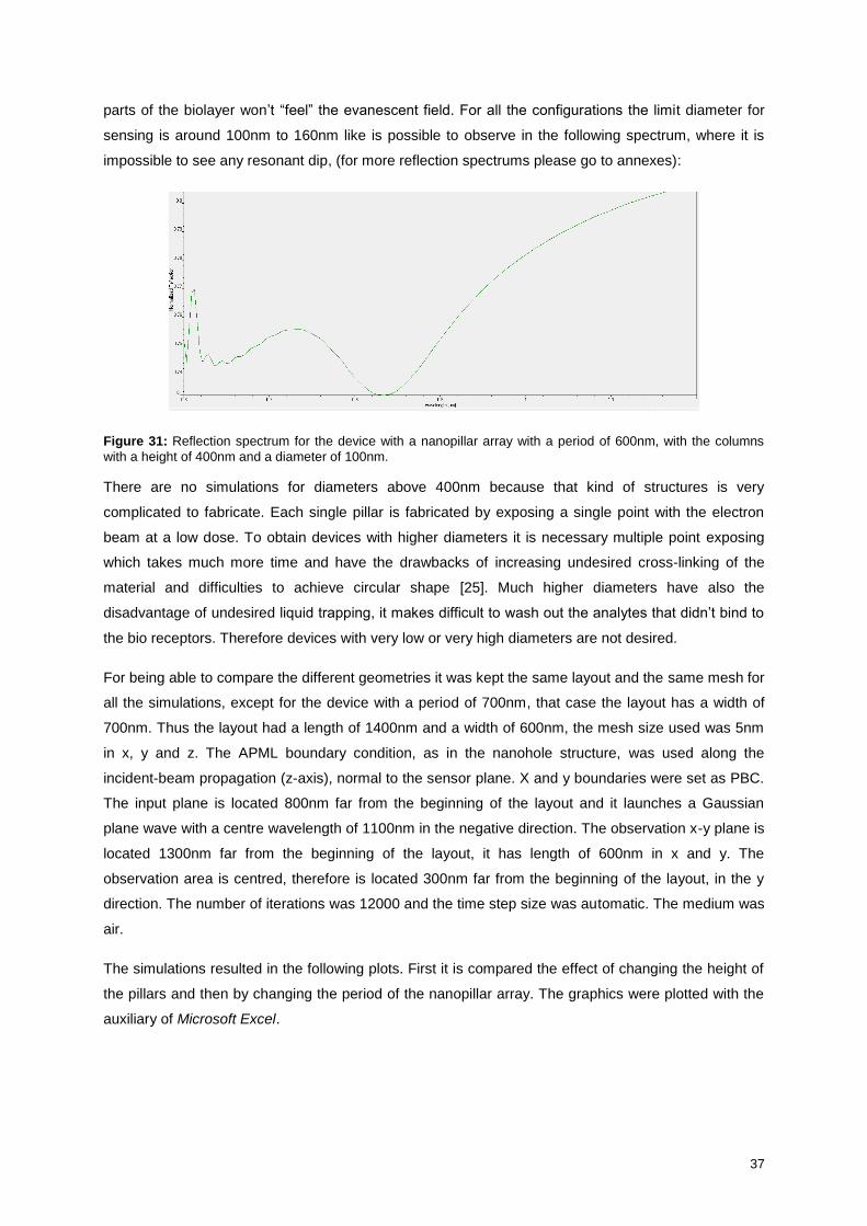
37
parts of the biolayer won’t “feel” the evanescent field. For all the configurations the limit diameter for
sensing is around 100nm to 160nm like is possible to observe in the following spectrum, where it is
impossible to see any resonant dip, (for more reflection spectrums please go to annexes):
Figure 31: Reflection spectrum for the device with a nanopillar array with a period of 600nm, with the columns
with a height of 400nm and a diameter of 100nm.
There are no simulations for diameters above 400nm because that kind of structures is very
complicated to fabricate. Each single pillar is fabricated by exposing a single point with the electron
beam at a low dose. To obtain devices with higher diameters it is necessary multiple point exposing
which takes much more time and have the drawbacks of increasing undesired cross-linking of the
material and difficulties to achieve circular shape [25]. Much higher diameters have also the
disadvantage of undesired liquid trapping, it makes difficult to wash out the analytes that didn’t bind to
the bio receptors. Therefore devices with very low or very high diameters are not desired.
For being able to compare the different geometries it was kept the same layout and the same mesh for
all the simulations, except for the device with a period of 700nm, that case the layout has a width of
700nm. Thus the layout had a length of 1400nm and a width of 600nm, the mesh size used was 5nm
in x, y and z. The APML boundary condition, as in the nanohole structure, was used along the
incident-beam propagation (z-axis), normal to the sensor plane. X and y boundaries were set as PBC.
The input plane is located 800nm far from the beginning of the layout and it launches a Gaussian
plane wave with a centre wavelength of 1100nm in the negative direction. The observation x-y plane is
located 1300nm far from the beginning of the layout, it has length of 600nm in x and y. The
observation area is centred, therefore is located 300nm far from the beginning of the layout, in the y
direction. The number of iterations was 12000 and the time step size was automatic. The medium was
air.
The simulations resulted in the following plots. First it is compared the effect of changing the height of
the pillars and then by changing the period of the nanopillar array. The graphics were plotted with the
auxiliary of Microsoft Excel.
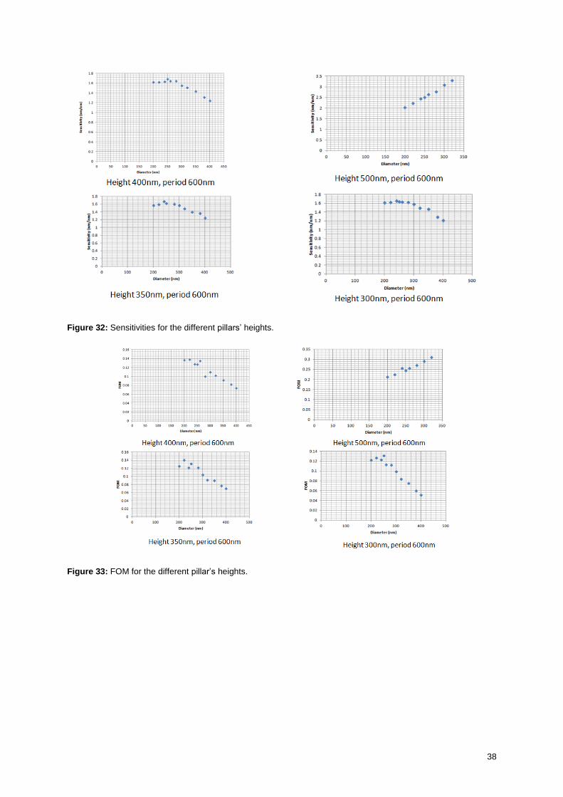
38
Figure 32: Sensitivities for the different pillars’ heights.
Figure 33: FOM for the different pillar’s heights.
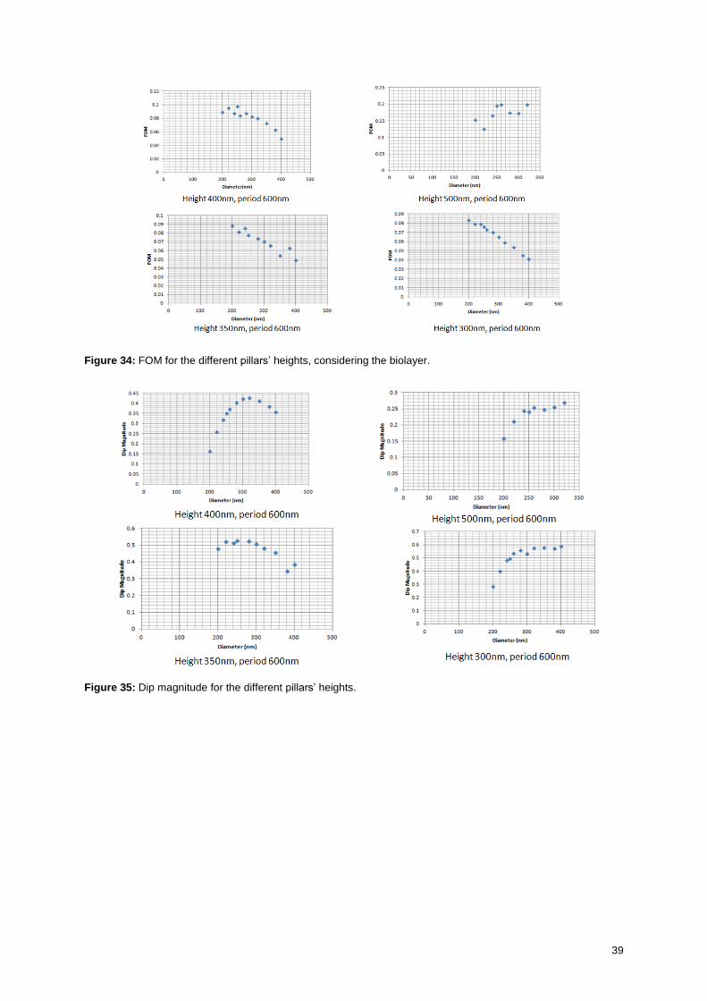
39
Figure 34: FOM for the different pillars’ heights, considering the biolayer.
Figure 35: Dip magnitude for the different pillars’ heights.
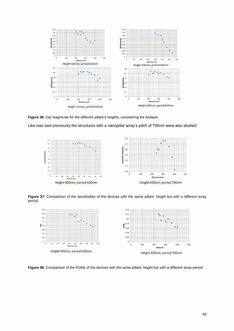
40
Figure 36: Dip magnitude for the different pillars’s heights, considering the biolayer.
Like was said previously the structures with a nanopillar array’s pitch of 700nm were also studied:
Figure 37: Comparison of the sensitivities of the devices with the same pillars’ height but with a different array
period.
Figure 38: Comparison of the FOMs of the devices with the same pillars’ height but with a different array period.
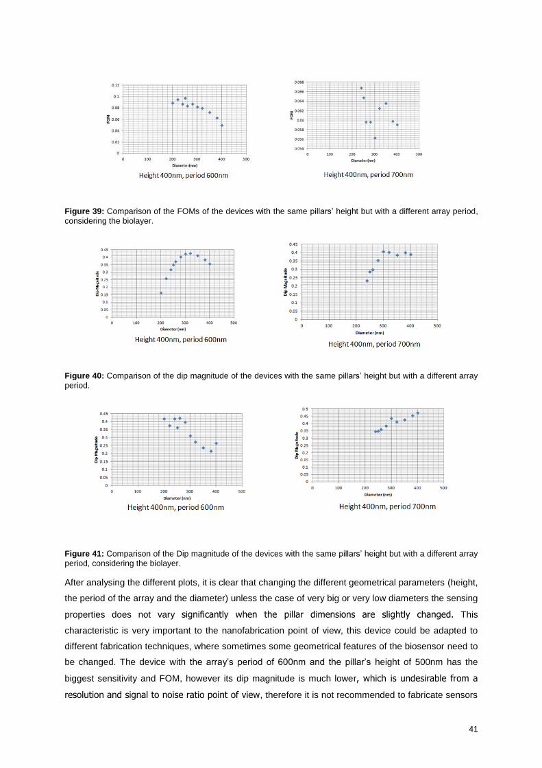
41
Figure 39: Comparison of the FOMs of the devices with the same pillars’ height but with a different array period,
considering the biolayer.
Figure 40: Comparison of the dip magnitude of the devices with the same pillars’ height but with a different array
period.
Figure 41: Comparison of the Dip magnitude of the devices with the same pillars’ height but with a different array
period, considering the biolayer.
After analysing the different plots, it is clear that changing the different geometrical parameters (height,
the period of the array and the diameter) unless the case of very big or very low diameters the sensing
properties does not vary significantly when the pillar dimensions are slightly changed. This
characteristic is very important to the nanofabrication point of view, this device could be adapted to
different fabrication techniques, where sometimes some geometrical features of the biosensor need to
be changed. The device with the array’s period of 600nm and the pillar’s height of 500nm has the
biggest sensitivity and FOM, however its dip magnitude is much lower, which is undesirable from a
resolution and signal to noise ratio point of view, therefore it is not recommended to fabricate sensors
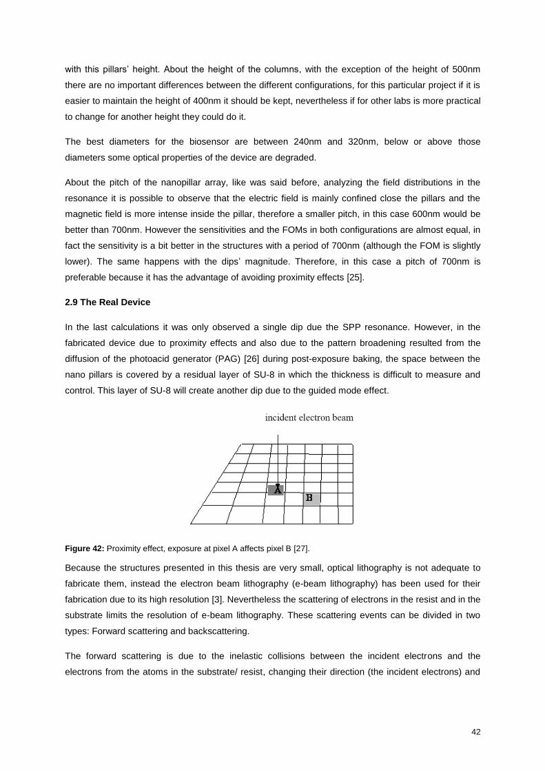
42
with this pillars’ height. About the height of the columns, with the exception of the height of 500nm
there are no important differences between the different configurations, for this particular project if it is
easier to maintain the height of 400nm it should be kept, nevertheless if for other labs is more practical
to change for another height they could do it.
The best diameters for the biosensor are between 240nm and 320nm, below or above those
diameters some optical properties of the device are degraded.
About the pitch of the nanopillar array, like was said before, analyzing the field distributions in the
resonance it is possible to observe that the electric field is mainly confined close the pillars and the
magnetic field is more intense inside the pillar, therefore a smaller pitch, in this case 600nm would be
better than 700nm. However the sensitivities and the FOMs in both configurations are almost equal, in
fact the sensitivity is a bit better in the structures with a period of 700nm (although the FOM is slightly
lower). The same happens with the dips’ magnitude. Therefore, in this case a pitch of 700nm is
preferable because it has the advantage of avoiding proximity effects [25].
2.9 The Real Device
In the last calculations it was only observed a single dip due the SPP resonance. However, in the
fabricated device due to proximity effects and also due to the pattern broadening resulted from the
diffusion of the photoacid generator (PAG) [26] during post-exposure baking, the space between the
nano pillars is covered by a residual layer of SU-8 in which the thickness is difficult to measure and
control. This layer of SU-8 will create another dip due to the guided mode effect.
Figure 42: Proximity effect, exposure at pixel A affects pixel B [27].
Because the structures presented in this thesis are very small, optical lithography is not adequate to
fabricate them, instead the electron beam lithography (e-beam lithography) has been used for their
fabrication due to its high resolution [3]. Nevertheless the scattering of electrons in the resist and in the
substrate limits the resolution of e-beam lithography. These scattering events can be divided in two
types: Forward scattering and backscattering.
The forward scattering is due to the inelastic collisions between the incident electrons and the
electrons from the atoms in the substrate/ resist, changing their direction (the incident electrons) and
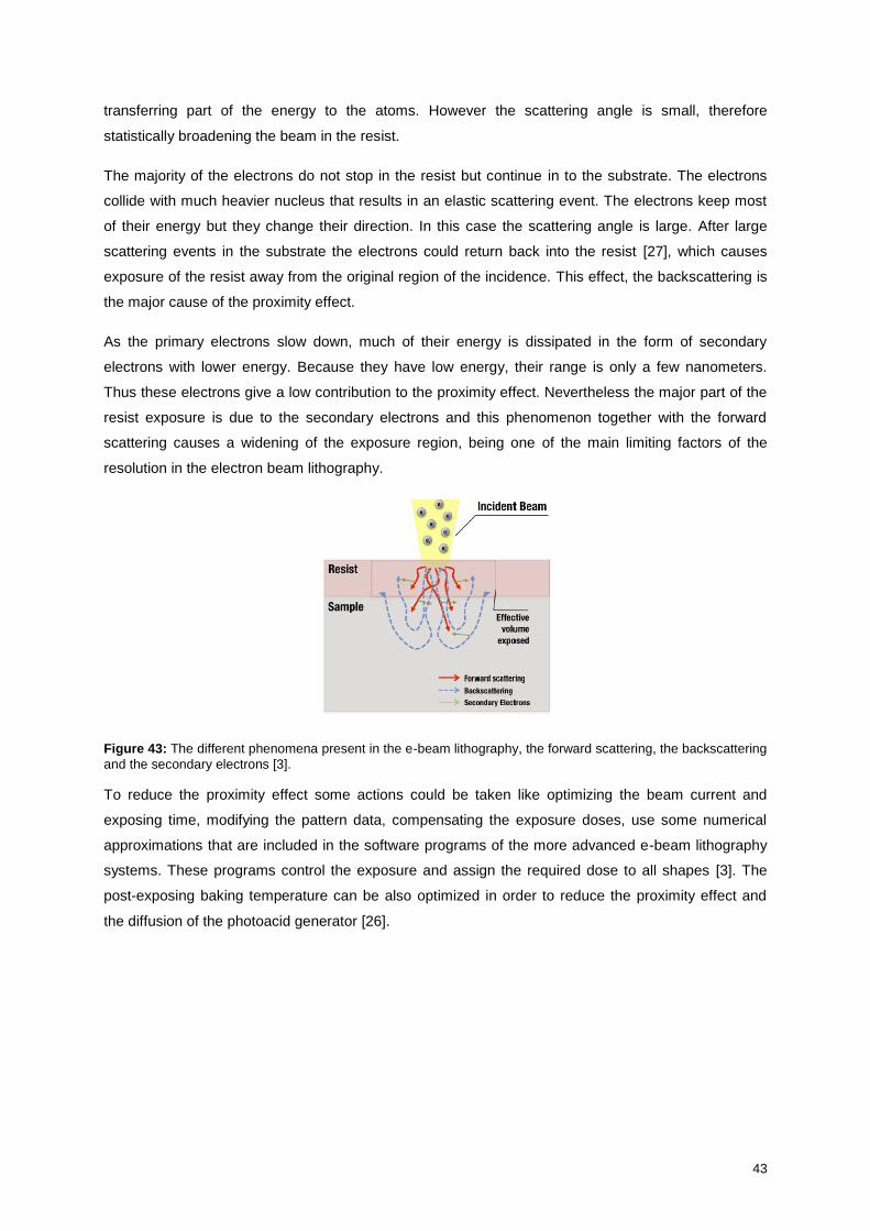
43
transferring part of the energy to the atoms. However the scattering angle is small, therefore
statistically broadening the beam in the resist.
The majority of the electrons do not stop in the resist but continue in to the substrate. The electrons
collide with much heavier nucleus that results in an elastic scattering event. The electrons keep most
of their energy but they change their direction. In this case the scattering angle is large. After large
scattering events in the substrate the electrons could return back into the resist [27], which causes
exposure of the resist away from the original region of the incidence. This effect, the backscattering is
the major cause of the proximity effect.
As the primary electrons slow down, much of their energy is dissipated in the form of secondary
electrons with lower energy. Because they have low energy, their range is only a few nanometers.
Thus these electrons give a low contribution to the proximity effect. Nevertheless the major part of the
resist exposure is due to the secondary electrons and this phenomenon together with the forward
scattering causes a widening of the exposure region, being one of the main limiting factors of the
resolution in the electron beam lithography.
Figure 43: The different phenomena present in the e-beam lithography, the forward scattering, the backscattering
and the secondary electrons [3].
To reduce the proximity effect some actions could be taken like optimizing the beam current and
exposing time, modifying the pattern data, compensating the exposure doses, use some numerical
approximations that are included in the software programs of the more advanced e-beam lithography
systems. These programs control the exposure and assign the required dose to all shapes [3]. The
post-exposing baking temperature can be also optimized in order to reduce the proximity effect and
the diffusion of the photoacid generator [26].
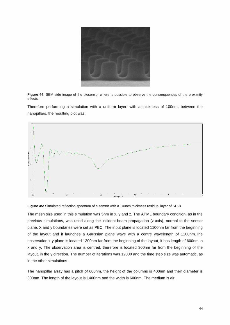
44
Figure 44: SEM side image of the biosensor where is possible to observe the consenquences of the proximity
effects.
Therefore performing a simulation with a uniform layer, with a thickness of 100nm, between the
nanopillars, the resulting plot was:
Figure 45: Simulated reflection spectrum of a sensor with a 100nm thickness residual layer of SU-8.
The mesh size used in this simulation was 5nm in x, y and z. The APML boundary condition, as in the
previous simulations, was used along the incident-beam propagation (z-axis), normal to the sensor
plane. X and y boundaries were set as PBC. The input plane is located 1100nm far from the beginning
of the layout and it launches a Gaussian plane wave with a centre wavelength of 1100nm.The
observation x-y plane is located 1300nm far from the beginning of the layout, it has length of 600nm in
x and y. The observation area is centred, therefore is located 300nm far from the beginning of the
layout, in the y direction. The number of iterations was 12000 and the time step size was automatic, as
in the other simulations.
The nanopillar array has a pitch of 600nm, the height of the columns is 400nm and their diameter is
300nm. The length of the layout is 1400nm and the width is 600nm. The medium is air.
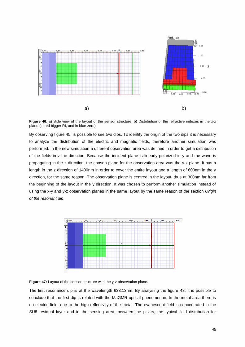
45
Figure 46: a) Side view of the layout of the sensor structure. b) Distribution of the refractive indexes in the x-z
plane (in red bigger RI, and in blue zero).
By observing figure 45, is possible to see two dips. To identify the origin of the two dips it is necessary
to analyze the distribution of the electric and magnetic fields, therefore another simulation was
performed. In the new simulation a different observation area was defined in order to get a distribution
of the fields in z the direction. Because the incident plane is linearly polarized in y and the wave is
propagating in the z direction, the chosen plane for the observation area was the y-z plane. It has a
length in the z direction of 1400nm in order to cover the entire layout and a length of 600nm in the y
direction, for the same reason. The observation plane is centred in the layout, thus at 300nm far from
the beginning of the layout in the y direction. It was chosen to perform another simulation instead of
using the x-y and y-z observation planes in the same layout by the same reason of the section Origin
of the resonant dip.
Figure 47: Layout of the sensor structure with the y-z observation plane.
The first resonance dip is at the wavelength 638.13nm. By analysing the figure 48, it is possible to
conclude that the first dip is related with the MaGMR optical phenomenon. In the metal area there is
no electric field, due to the high reflectivity of the metal. The evanescent field is concentrated in the
SU8 residual layer and in the sensing area, between the pillars, the typical field distribution for
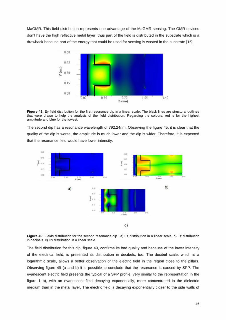
46
MaGMR. This field distribution represents one advantage of the MaGMR sensing. The GMR devices
don’t have the high reflective metal layer, thus part of the field is distributed in the substrate which is a
drawback because part of the energy that could be used for sensing is wasted in the substrate [15].
Figure 48: Ey field distribution for the first resonance dip in a linear scale. The black lines are structural outlines
that were drawn to help the analysis of the field distribution. Regarding the colours, red is for the highest amplitude and blue for the lowest.
The second dip has a resonance wavelength of 792.24nm. Observing the figure 45, it is clear that the
quality of the dip is worse, the amplitude is much lower and the dip is wider. Therefore, it is expected
that the resonance field would have lower intensity.
Figure 49: Fields distribution for the second resonance dip. a) Ez distribution in a linear scale. b) Ez distribution
in decibels. c) Hx distribution in a linear scale.
The field distribution for this dip, figure 49, confirms its bad quality and because of the lower intensity
of the electrical field, is presented its distribution in decibels, too. The decibel scale, which is a
logarithmic scale, allows a better observation of the electric field in the region close to the pillars.
Observing figure 49 (a and b) it is possible to conclude that the resonance is caused by SPP. The
evanescent electric field presents the typical of a SPP profile, very similar to the representation in the
figure 1 b), with an evanescent field decaying exponentially, more concentrated in the dielectric
medium than in the metal layer. The electric field is decaying exponentially closer to the side walls of
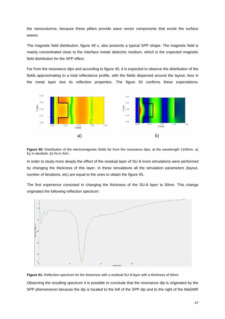
47
the nanocolumns, because these pillars provide wave vector components that excite the surface
waves.
The magnetic field distribution, figure 49 c, also presents a typical SPP shape. The magnetic field is
mainly concentrated close to the interface metal/ dielectric medium, which is the expected magnetic
field distribution for the SPP effect.
Far from the resonance dips and according to figure 45, it is expected to observe the distribution of the
fields approximating to a total reflectance profile, with the fields dispersed around the layout, less in
the metal layer due its reflection properties. The figure 50 confirms these expectations:
Figure 50: Distribution of the electromagnetic fields far from the resonance dips, at the wavelength 1100nm. a)
Ey in decibels. b) Hx in A/m.
In order to study more deeply the effect of the residual layer of SU-8 more simulations were performed
by changing the thickness of this layer. In these simulations all the simulation parameters (layout,
number of iterations, etc) are equal to the ones to obtain the figure 45.
The first experience consisted in changing the thickness of the SU-8 layer to 50nm. This change
originated the following reflection spectrum:
Figure 51: Reflection spectrum for the biosensor with a residual SU-8 layer with a thickness of 50nm.
Observing the resulting spectrum it is possible to conclude that the resonance dip is originated by the
SPP phenomenon because the dip is located to the left of the SPP dip and to the right of the MaGMR
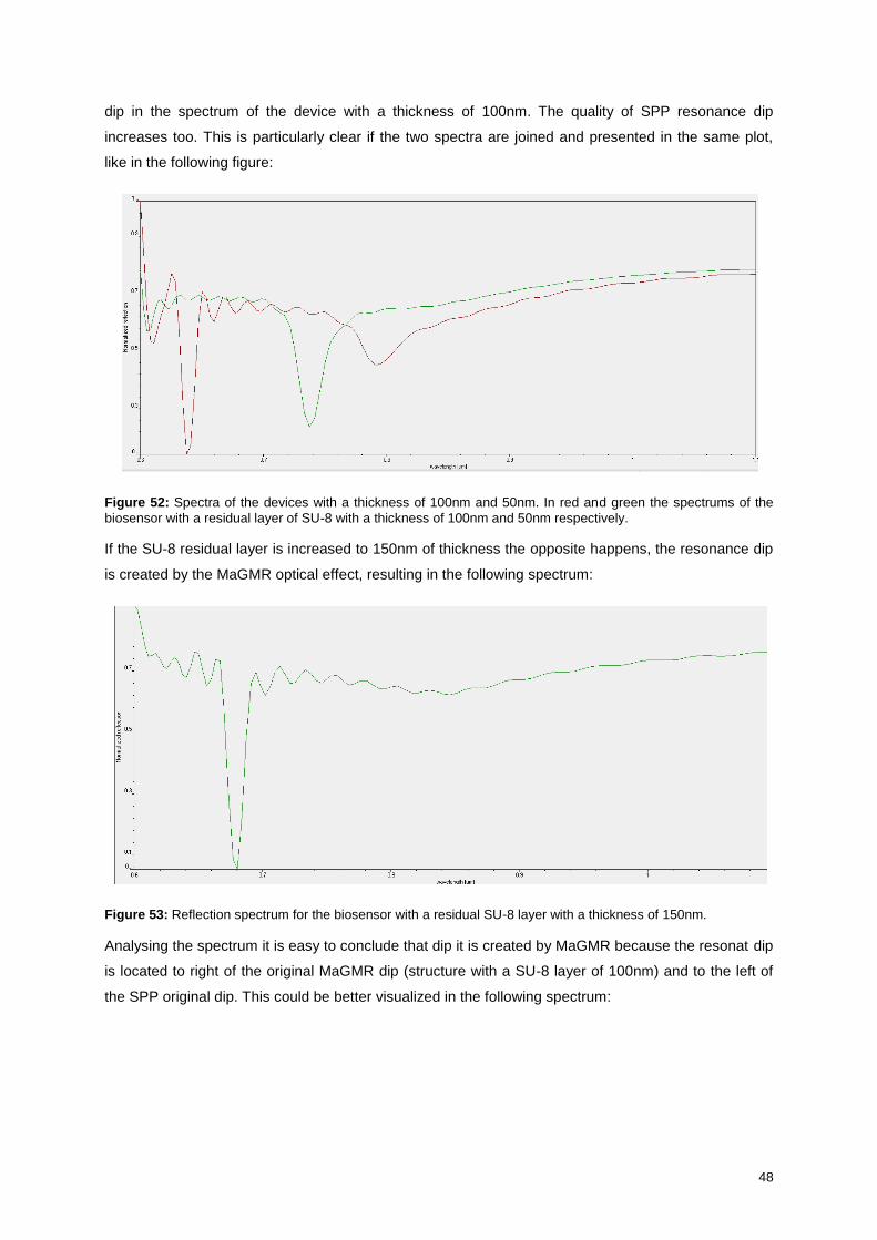
48
dip in the spectrum of the device with a thickness of 100nm. The quality of SPP resonance dip
increases too. This is particularly clear if the two spectra are joined and presented in the same plot,
like in the following figure:
Figure 52: Spectra of the devices with a thickness of 100nm and 50nm. In red and green the spectrums of the
biosensor with a residual layer of SU-8 with a thickness of 100nm and 50nm respectively.
If the SU-8 residual layer is increased to 150nm of thickness the opposite happens, the resonance dip
is created by the MaGMR optical effect, resulting in the following spectrum:
Figure 53: Reflection spectrum for the biosensor with a residual SU-8 layer with a thickness of 150nm.
Analysing the spectrum it is easy to conclude that dip it is created by MaGMR because the resonat dip
is located to right of the original MaGMR dip (structure with a SU-8 layer of 100nm) and to the left of
the SPP original dip. This could be better visualized in the following spectrum:
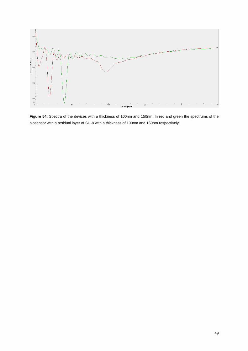
49
Figure 54: Spectra of the devices with a thickness of 100nm and 150nm. In red and green the spectrums of the
biosensor with a residual layer of SU-8 with a thickness of 100nm and 150nm respectively.
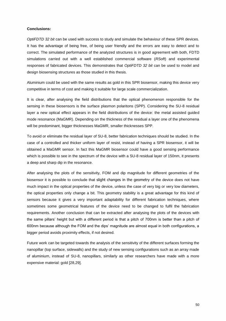
50
Conclusions:
OptiFDTD 32 bit can be used with success to study and simulate the behaviour of these SPR devices.
It has the advantage of being free, of being user friendly and the errors are easy to detect and to
correct. The simulated performance of the analyzed structures is in good agreement with both, FDTD
simulations carried out with a well established commercial software (RSoft) and experimental
responses of fabricated devices. This demonstrates that OptiFDTD 32 bit can be used to model and
design biosensing structures as those studied in this thesis.
Aluminium could be used with the same results as gold in this SPR biosensor, making this device very
competitive in terms of cost and making it suitable for large scale commercialization.
It is clear, after analysing the field distributions that the optical phenomenon responsible for the
sensing in these biosensors is the surface plasmon polaritons (SPP). Considering the SU-8 residual
layer a new optical effect appears in the field distributions of the device: the metal assisted guided
mode resonance (MaGMR). Depending on the thickness of the residual a layer one of the phenomena
will be predominant, bigger thicknesses MaGMR, smaller thicknesses SPP.
To avoid or eliminate the residual layer of SU-8, better fabrication techniques should be studied. In the
case of a controlled and thicker uniform layer of resist, instead of having a SPR biosensor, it will be
obtained a MaGMR sensor. In fact this MaGMR biosensor could have a good sensing performance
which is possible to see in the spectrum of the device with a SU-8 residual layer of 150nm, it presents
a deep and sharp dip in the resonance.
After analysing the plots of the sensitivity, FOM and dip magnitude for different geometries of the
biosensor it is possible to conclude that slight changes in the geometry of the device does not have
much impact in the optical properties of the device, unless the case of very big or very low diameters,
the optical properties only change a bit. This geometry stability is a great advantage for this kind of
sensors because it gives a very important adaptability for different fabrication techniques, where
sometimes some geometrical features of the device need to be changed to fulfil the fabrication
requirements. Another conclusion that can be extracted after analysing the plots of the devices with
the same pillars’ height but with a different period is that a pitch of 700nm is better than a pitch of
600nm because although the FOM and the dips’ magnitude are almost equal in both configurations, a
bigger period avoids proximity effects, if not desired.
Future work can be targeted towards the analysis of the sensitivity of the different surfaces forming the
nanopillar (top surface, sidewalls) and the study of new sensing configurations such as an array made
of aluminium, instead of SU-8, nanopillars, similarly as other researchers have made with a more
expensive material: gold [28,29].
51
References:
[1] Álvarez, J. Á. (2013). Development of a polarimetric based optical biosensor using a free standing porous
membrane. Departamento de Física Aplicada, Universitade de València .
[2] M. Holgado, C. A. Barrios, F.J Ortega; F.J. Sanza, R. Casquel, M.F Laguna, M.J Bañuls, D.López-Romero, R.
Puchades, A. Maquieira (2010). Label-free biosensing by means of periodic lattices of high aspect. Biosensors
and Bioelectronics , 25, 2553–2558.
[3] Freitas, S. (2014). Slides from classes. Instituto Superior Técnico, Universidade de Lisboa.
[4] Conde, J. P. (2013). Slides from classes. Instituto Superior Técnico, Universidade de Lisboa.
[5] Gautschi, G. (2002). Piezoelectric Sensorics: Force, Strain, Pressure, Acceleration and Acoustic Emission
Sensors, Materials and Amplifiers. Springer Science & Business Media.
[6] Kathryn M. Mayer, J. H. (2011). Localized Surface Plasmon Resonance Sensors. Chemical Reviews, ACS
Publications, 111, 3828 – 3857.
[7] W. Andrew Murray, W. L. (2007). Plasmonic Materials. Advanced Materials, 19, 3771–3782.
[8] Guangyuan Si, Y. Z. (2014). Liquid-Crystal-Enabled Active Plasmonics: A Review. Materials, 7, 1296-1317.
[9] Daiying Zhang, L. M. (2011). Microfabrication and Applications of Opto-Microfluidic Sensors. Sensors , 11,
1424-8220.
[10] Ruffato, G., Zacco, G., Romanato, F. (2012). Innovative Exploitation of Grating-Coupled. In Plasmonics -
Principles and Applications (pp. 419-44). InTech.
[11] Fonseca, L. (2014). Slides from classes. Instituto Superior Técnico, Universidade de Lisboa
[12] 21st Century Electromagnetics. (n.d.). Retrieved from
http://emlab.utep.edu/ee5390em21/Lecture%2011%20--%20Guided%20mode%20resonance.pdf.
[13] Li, Y., Srimathi, I. R., Woodward, R. H., Pung, A. J., Poutous, M. K. (2012). Guided-Mode Resonance Filters
for Wavelength Selection in Mid-Infrared Fiber Lasers. IEEE PHOTONICS TECHNOLOGY LETTERS , 24, 2300-
2303.
[14] Jia, K., Zhang, D., & Ma, J. (2011). Sensitivity of guided mode resonance filter-based biosensor in visible and
near infrared ranges. Sensors and Actuators B: Chemical , 156, 194–197.
[15] Lin, S.-F., Wang, C.-M., Ding, T.-J., Tsai, Y.-L., Yang, T.-H., Chen, W.-Y., et al. (2012). Sensitive metal layer
assisted guided mode resonance biosensor with a spectrum inversed response and strong asymmetric resonance
field distribution. OPTICS EXPRESS , 20, 14584-14594.
[16] Retrieved from http://ab-initio.mit.edu/wiki/index.php/Yee_lattice.
[17] Retrieved from http://emlab.utep.edu/index.htm.
[18] Optiwave. (2013). OptiFDTD Technical Background.
[19] Retrieved from http://www.bloomberg.com/research/stocks/private/snapshot.asp?privcapid=1526333.
52
[20] Optiwave. (2013). OptiFDTD Tutorials.
[21] Retrieved from http://optiwave.com/products/component-design/optifdtd/optical-fdtd/.
[22] Canalejas-Tejero, V., Herranz, S., Bellingham, A., Moreno-Bondi, M. C., Barrios, C. A. (2013). Passivated
Aluminum Nanohole Arrays for Label-Free Biosensing Applications. Applied Materials and Interfaces , 6, A-F.
[23] Holgado, M., Barrios, C., Sanza, F., Casquela, R., Laguna, M., & F.J. Ortegac. (2010). Label-free biosensing
by means of periodic lattices of high aspect ratio SU-8 nano-pillars. Biosensors and Bioelectronics ,25, 2553-
2558.
[24] Gauglitz, G. (2005). Multiple reflectance interference spectroscopy measurements made. REVIEW OF
SCIENTIFIC INSTRUMENTS , 76, 1-10.
[25] Casquel, R., Holgado, M., Sanza, F. J., Laguna, M. F., Barrios, C. A., López-Romero, D., et al. (2011).
Optimization of a label-free biosensor vertically characterized based on a periodic lattice of high aspect ratio SU-8
nano-pillars with a simplified 2D theoretical model. PSS , 8, 1087–1092.
[26] López-Romero, D., Barrios, C., Holgado, M., Laguna, M., & Casquel, R. (2010). High aspect-ratio SU-8 resist
nano-pillar lattice by e-beam direct writing and its application for liquid trapping. Microelectronic Engineering , 87,
663–667.
[27] Retrieved from http://nanolithography.gatech.edu/proximity.htm.
[28] Victoria Kugel, H.-F. J. (2014). Nanopillars for Sensing. Journal of Nanoscience and Nanotechnology , 14,
6469–6477.
[29] Çetin, A. E., Yanik, A. A., Yilmaz, C., Somu, S., Busnaina, A., & Altug, H. (2011). Monopole antenna arrays
for optical trapping, spectroscopy, and sensing. APPLIED PHYSICS LETTERS , 98, 1-3.
[30] Rodrigo, S. G., García-Vidal, F. J., & Martín-Moreno, L. (2008). Influence of material properties on
extraordinary optical transmission through hole arrays. PHYSICAL REVIEW B , 77, 075401 1-8.
[31] West, P. R., Ishii, S., Naik, G. V., Emani, N. K.,Shalaev, V. M, Boltasseva (2010). Searching for better
plasmonic materials. Lasers and Photonics Reviews, 4, 795-808.
[32] Retrieved from http://www.bloomberg.com/markets/commodities/futures/metals.
[33] Langhammer, C., Schwind, M., asemo, B., ori , I. (2008). Localized Surface Plasmon Resonances in
Aluminum Nanodisks. Nano Letters , 8, 1461−1471
[34] Su, W., Zheng, G., & Li, X. (2012). Design of a highly sensitive surface plasmon resonance sensor using
aluminum-based diffraction grating. Optics Communications , 285, 4603−4607
[35] Yokogawa, S., Burgos, S., & Atwater, H. (2012). Plasmonic Color Filters for CMOS Image Sensor
Applications. Nano Letters , 12, 4349−4354.
53
Annexes:
Annexe 1: Reflection Spectrum for the nanopillar array with a period of 600nm and columns with a height of
300nm and diameter of 150nm.
Annexe 2: Reflection Spectrum for the nanopillar array with a period of 600nm and columns with a height of
350nm and diameter of 160nm.
54
Annexe 3: Reflection Spectrum for the nanopillar array with a period of 600nm and columns with a height of
500nm and diameter of 150nm.
Annexe 4: Reflection Spectrum for the nanopillar array with a period of 700nm and columns with a height of
400nm and diameter of 220nm.
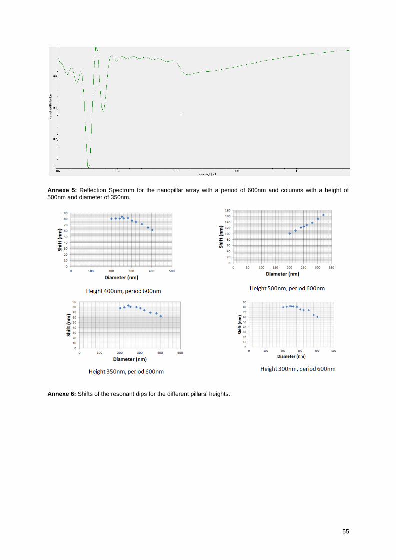
55
Annexe 5: Reflection Spectrum for the nanopillar array with a period of 600nm and columns with a height of
500nm and diameter of 350nm.
Annexe 6: Shifts of the resonant dips for the different pillars’ heights.
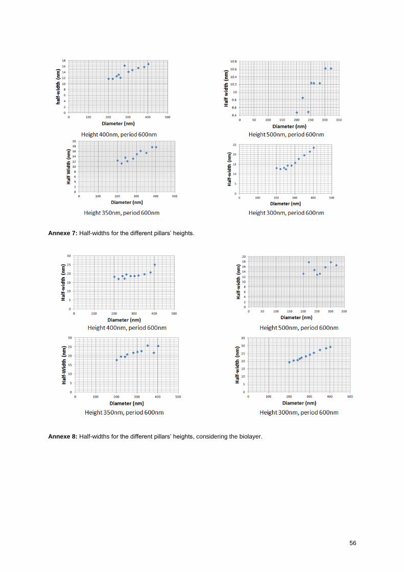
56
Annexe 7: Half-widths for the different pillars’ heights.
Annexe 8: Half-widths for the different pillars’ heights, considering the biolayer.
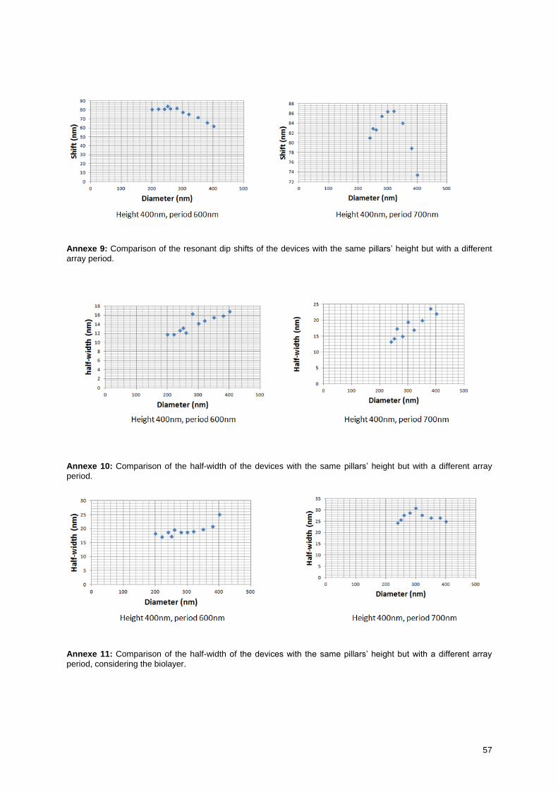
57
Annexe 9: Comparison of the resonant dip shifts of the devices with the same pillars’ height but with a different
array period.
Annexe 10: Comparison of the half-width of the devices with the same pillars’ height but with a different array
period.
Annexe 11: Comparison of the half-width of the devices with the same pillars’ height but with a different array
period, considering the biolayer.

58

59


![Optical Biosensors [Online]-1 - Walter Scott, Jr. College of … · · 2008-12-171 Optical Biosensors First Semester Report Fall Semester 2008 by ... The yellow shows the gold electrodes](https://img.pdfslide.net/doc/110x75/5ae44c567f8b9ae74a8eea87/optical-biosensors-online-1-walter-scott-jr-college-of-optical-biosensors.jpg)