Embed Size (px)
Citation preview
Design of Novel Pixel with Non-Uniform Doped
Transistor Channel and Triangle-Tooth Shape
Pinned Photodiode for High Speed CMOS Image
Sensors
Weihui Liu, Xiangliang Jin, Hongjiao Yang, Lizhen Tang, and Jia Yang School of Physics and Optoelectronics, Xiangtan University, Xiangtan, 411105, China
Hunan Engineering Laboratory for Microelectronics, Optoelectronics and System on a Chip, Xiangtan, 411105, China
Email: {liuweihuiotter, tanglizhen0801, javayang4}@163.com, {jinxl, yanghongjiao2004}@xtu.edu.cn
Abstract—A novel pixel structure, which is achieved by
generating a non-uniform doped transfer transistor channel
and shaping a PPD (Pinned Photodiode) like triangular
tooth, has been designed to enhance the electron transfer
speed. In this study, comparative analysis is carried out to
make detailed comparisons between conventional
rectangular PPD and the new proposed structure. Triangle-
tooth shape PPD not only maintains superiorities of high
light sensitivity, but also boosts charge transfer speed. To
verify its advantages, theoretical analysis and TCAD 3D
device simulations were provided during the course of
research. Simulations show that the charge transfer time
can effectively decrease from 322ns to 9.6ns. Furthermore,
charge transfer efficiency can greatly enhance from 54 e-/ns
to 1052 e-/ns, 19.48 times increment compared to traditional
rectangular PPD.
Index Terms—pinned photodiode, charge transfer speed,
TCAD 3D device simulations, image lag
I. INTRODUCTION
High speed CMOS image sensors are widely used in
surveillance, machine vision camera, traffic monitoring,
scientific motion capture and collision detection. To
realize these applications, the image sensors not only
have high sensitivity, high full well capacity, low dark
current, and low noise, but also obtain no image lag and
fast readout speed [1]. There are five factors which limit
the readout speed [2]. (I) Settling time for the pixel drive
signals. (II) The photo-electrons transit time from the
Large Pined Photodiode (PPD) to Floating Diffusion
(FD). (III) Readout time from the pixel to the column line.
(IV) Signal processing time in the column circuits. (V)
Readout time from the column circuits to the chip output.
In this paper, we demonstrate a developed PPD structure
which improves the factor (II).
There are two important design issues in high speed
PPD design. On one hand, since the exposure time is very
short, large-area PPD is required to improve the
sensitivity illumination.
large-area PPD results in weak lateral electric field,
making it difficult to transfer all the photon-generated
electrons from the photodiode to the floating diffusion.
This insufficient transfer results in image lag [3]. Image
lag and the photo-electrons transit time of PPD are
mainly determined by the charge transfer efficiency.
Charge transfer efficiency of PPD is the percentage of
photo-electrons which is successfully transferred and the
charge transfer time. Therefore, researching on methods
to enhance the charge transfer efficiency of PPD with
large size is of great significance.
Some approaches that investigation on how to speed
up electrons transfer have been reported. The first
approach is to control the n-layer dopant concentration
[4]. By using this approach, it is possible both to enlarge
the n-layer region and to create an electric field toward
the FD, however, some additional photomasks or extra
processes are necessary. The second approach is to
optimize electrical potential distribution in the connection
region between the transfer gate channel and the PPD by
using an L-shaped or peninsula-shaped transfer gate [5],
[6].
In this work, we present a non-uniform doped transfer
gate channel and a triangle-tooth shape PPD, which is
introduced to provide an ascending electrical potential
gradient in the transfer gate channel and improve lateral
electric field in PPD, respectively. Image lag analysis of
PPD is described in Section 2. Simulation results and
optimization are shown in Section 3, and finally some
conclusions are given in Section 4.
II. PPD STRUCTURE AND PROBLEM STATEMENT
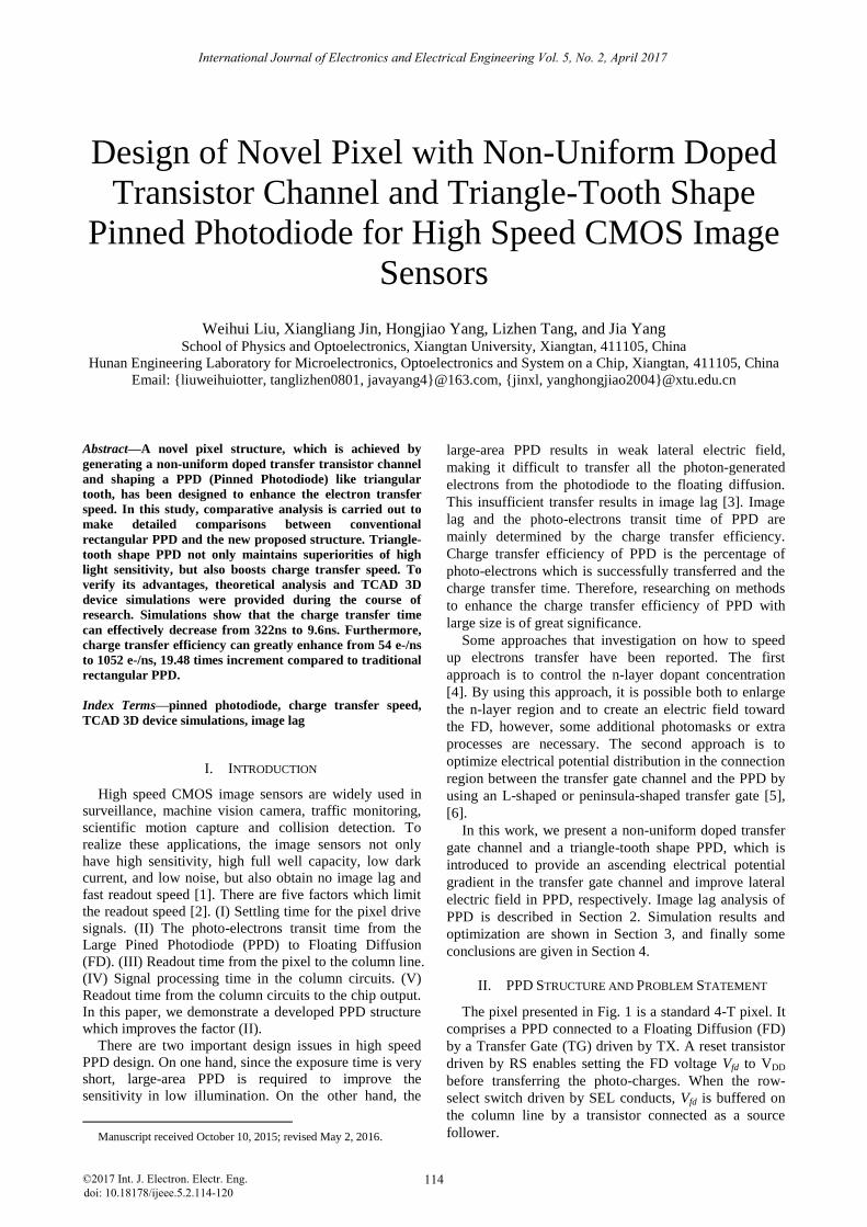
The pixel presented in Fig. 1 is a standard 4-T pixel. It
comprises a PPD connected to a Floating Diffusion (FD)
by a Transfer Gate (TG) driven by TX. A reset transistor
driven by RS enables setting the FD voltage Vfd to VDD
before transferring the photo-charges. When the row-
select switch driven by SEL conducts, Vfd is buffered on
the column line by a transistor connected as a source
follower.
Manuscript received October 10, 2015; revised May 2, 2016.
International Journal of Electronics and Electrical Engineering Vol. 5, No. 2, April 2017
©2017 Int. J. Electron. Electr. Eng. 114doi: 10.18178/ijeee.5.2.114-120
On the other hand, thein low
The PPD consists of a p+ pinned layer, a buried n-
layer, and a p− substrate. Two depletion regions form at
the p+/n− and n−/p−sub junctions. With suitable
implantation and annealing steps, these two depletion
regions join and thus form a region free of mobile carriers
and electrically isolated from the substrate. When
photons impinge on the PPD, the photo-generated
electrons move to the maximum electrostatic potential
within the PPD whereas holes are rejected to the substrate.
At the end of the illumination phase, the photo-charges
are transferred to the FD, where a charge-to-voltage
conversion takes place on the parasitic capacitor. And
TGVT is the TG channel doping layer for adjusting
threshold voltage. The impurity concentration in TGVT
layer is lower than the p+ pinned layer.
Figure 1. 4-T pixel with depletion regions shown on a vertical slice of the PPD.
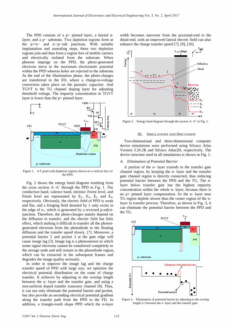
Fig. 2 shows the energy band diagram resulting from
the cross section A−A’ through the PPD in Fig. 1. The
conduction band, valence band, intrinsic Fermi level, and
Fermi level are represented by EC, EV, Ei, and EF,
respectively. Obviously, the electric field of PPD is weak
and flat, and a fringing field denoted by 1 only exists in
the edge of n-, which is generated by a reversed p-sub/n-
junction. Therefore, the photo-charges mainly depend on
the diffusion to transfer, and the electric field has little
effect, which making it difficult to transfer all the photon-
generated electrons from the photodiode to the floating
diffusion and the transfer speed slowly. [7]. Moreover, a
potential barrier 2 and pocket 3 at the gate edge will
cause image lag [3]. Image lag is a phenomenon in which
some signal electrons cannot be transferred completely to
the storage node and still remain in the photodiode region,
which can be extracted in the subsequent frames and
degrades the image quality seriously.
In order to improve the image lag and the charge
transfer speed of PPD with large size, we optimize the
electrical potential distribution on the route of charge
transfer. It achieves by adjusting to the overlap length
between the n- layer and the transfer gate, and using a
non-uniform doped transfer transistor channel [8]. Thus,
it can not only eliminate the potential barrier and pocket,
but also provide an ascending electrical potential gradient
along the transfer path from the PPD to the FD. In
addition, a triangle-tooth shape PPD which the n-layer
width becomes narrower from the proximal-end to the
distal-end, with an improved lateral electric field can also
enhance the charge transfer speed [7], [9], [10].
Figure 2. Energy band diagram through the section A−A’ in Fig. 1.
III. SIMULATIONS AND DISCUSSION
Two-dimensional and three-dimensional computer
device simulations were performed using Silvaco Atlas
Version 3.20.2R and Silvaco Atlas3D, respectively. The
device structure used in all simulations is shown in Fig. 1.
A. Elimination of Potential Barrier
A portion of the n- layer extends to the transfer gate
channel region, by keeping the n- layer and the transfer
gate channel region is directly connected, thus reducing
potential barrier between the PPD and the TG. The n-
layer below transfer gate has the highest impurity
concentration within the whole n- layer, because there is
no p+ pinned layer compensation. So the n- layer near
TG region deplete slower than the center region of the n-
layer in transfer process. Therefore, as shown in Fig. 3, it
can eliminate the potential barrier between the PPD and
the TG.
Figure 3. Elimination of potential barrier by adjusting to the overlap
length L1 between the n- layer and the transfer gate.
International Journal of Electronics and Electrical Engineering Vol. 5, No. 2, April 2017
©2017 Int. J. Electron. Electr. Eng. 115
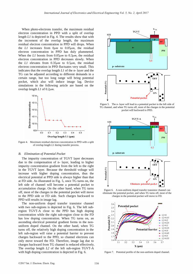
When photo-electrons transfer, the maximum residual
electron concentration in PPD with a split of overlap
length L1 is depicted in Fig. 4. The results show that with
the increment of the overlap length, the maximum
residual electron concentration in PPD will drops. When
the L1 increases from 0μm to 0.05μm, the residual
electron concentration in PPD has duly plummeted.
When the L1 boosts from 0.05μm to 0.3μm, the residual
electron concentration in PPD decreases slowly. When
the L1 elevates from 0.35μm to 0.5μm, the residual
electron concentration in PPD fluctuates very small. This
indicates that the overlap length L1 of the n- layer and the
TG can be adjusted according to different demands in a
certain range, but too long range will bring potential
pocket, which also will induce image lag. Device
simulations in the following article are based on the
overlap length L1 of 0.2μm.
Figure 4. Maximum residual electron concentration in PPD with a split of overlap length L1 during transfer process.
B. Elimination of Potential Pocket
The impurity concentration of TGVT layer decreases
due to the compensation of n- layer, leading to higher
impurity concentration gradient from the left to the right
in the TGVT layer. Because the threshold voltage will
increase with higher doping concentration, thus the
electrical potential at PPD side is always higher than that
at FD side. As illustrated in Fig. 5, once TG turns on, the
left side of channel will become a potential pocket to
accumulation charge. On the other hand, when TG turns
off, most of the charges in the potential pocket will move
to the PPD side or FD side. Such charges backward to
PPD will results in image lag.
The non-uniform doped transfer transistor channel
with two sub-regions is depicted in Fig. 6. The left sub-
region TGVT-A close to the PPD has high doping
concentration while the right sub-region close to the FD
has low doping concentration. When TG turns on, an
ascending electrical potential gradient forms in the non-
uniform doped channel. On the other hand, when TG
turns off, the relatively high doping concentration in the
left sub-region will raise a potential barrier to prevent
charges backward to the PPD, so channel electrons can
only move toward the FD. Therefore, image lag due to
charges backward from TG channel is reduced effectively.
The overlap length L2 of the left sub-region TGVT-A
with high doping concentration is depicted in Fig. 6.
Figure 5. The n- layer will lead to a potential pocket in the left side of TG channel, and when TG turns off, most of the charges in the potential
pocket will backward to PPD.
Figure 6. A non-uniform doped transfer transistor channel can eliminate the potential pocket, and when TG turns off, most of the
charges in the potential pocket will move to FD.
Figure 7. Potential profile of the non-uniform doped channel.
International Journal of Electronics and Electrical Engineering Vol. 5, No. 2, April 2017
©2017 Int. J. Electron. Electr. Eng. 116
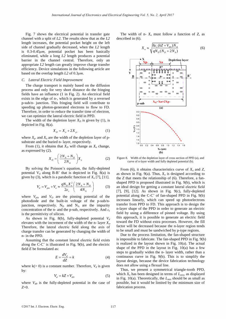
Fig. 7 shows the electrical potential in transfer gate
channel with a split of L2. The results show that as the L2
length increases, the potential pocket height on the left
side of channel gradually decreased, when the L2 length
is 0.3-0.45μm, potential pocket has been basically
eliminated, while a long L2 length produces a potential
barrier in the channel central. Therefore, only an
appropriate L2 length can greatly improve charge transfer
efficiency. Device simulations in the following article are
based on the overlap length L2 of 0.3μm.
C. Lateral Electric Field Improvement
The charge transport is mainly based on the diffusion
process and only for very short distance do the fringing
fields have an influence (1 in Fig. 2). An electrical field
exists in the edge of n-, which is generated by a reversed
p-sub/n- junction. This fringing field will contribute to
speeding up photon-generated electrons to flow to FD.
Therefore, in order to reduce the transfer time of electron,
we can optimize the lateral electric field in PPD.
The width of the depletion layer XD is given by (1), is
depicted in Fig. 8(a).
2D n pX X X (1)
where Xp- and Xn are the width of the depletion layer of p-
substrate and the buried n- layer, respectively.
From (1), it obtains that XD will change as Xn change,
as expressed by (2).
2
2
A D
D n
A
N NX X
N
(2)
By solving the Poisson’s equation, the fully-depleted
potential Vd along B-B’ that is depicted in Fig. 8(a) is
given by (3), which is a parabolic function of Xn [7], [11].
22
2 4
D n A D
d pin o
s A
qN X N NV V V
N
(3)
where Vpin and VO are the pinning potential of the
photodiode and the built-in voltage of the p-sub/n-
junction, respectively. ND and NA are the impurity
concentration of the n- and the p-sub, respectively. And εs
is the permittivity of silicon.
As shown in Fig. 8(b), fully-depleted potential Vd
elevates with the increment of the width of the n- layer Xn.
Therefore, the lateral electric field along the axis of
charge transfer can be generated by changing the width of
n- in the PPD.
Assuming that the constant lateral electric field exists
along the C-C’ is illustrated in Fig. 9(b), and the electric
field E be formulated as:
ddVE k
dZ (4)
where k(> 0) is a constant number. Therefore, Vd is given
by:
0d dV kZ V (5)
where Vd0 is the fully-depleted potential in the case of
Z=0.
The width of n- Xn must follow a function of Z, as
described in (6).
08 ( )
( 2 )
s d A
n
D D A
kZ V NX
qN N N
(6)
Figure 8. Width of the depletion layer of cross section of PPD (a), and curve of n-layer width and fully depleted potential (b).
From (6), it obtains characteristics curve of Xn and Z,
as shown in Fig. 9(a). Thus, Xn is designed according to
the Z that meets the relationship of (6). Therefore, a fan-
shaped PPD is proposed illustrated in Fig. 9(b), which is
an ideal design for getting a constant lateral electric field
[7], [9], [12]. As shown in Fig. 9(c), fully-depleted
potential along the C-C’ of fan-shaped PPD in Fig. 9(b)
increases linearly, which can speed up photoelectrons
transfer from PPD to FD. This approach is to design the
n-layer shape of the PPD in order to generate an electric
field by using a difference of pinned voltage. By using
this approach, it is possible to generate an electric field
toward the FD without extra processes. However, the fill
factor will be decreased because the n-layer region tends
to be small and must be sandwiched by p-type regions.
Due to the process limitation, the fan-shaped structure
is impossible to fabricate. The fan-shaped PPD in Fig. 9(b)
is realized in the layout shown in Fig. 10(a). The actual
shape of the PPD in the layout in Fig. 10(a) has a few
steps to gradually widen the n- layer width, rather than a
continuous curve in Fig. 9(b). This is to simplify the
layout design, because the device fabrication technology
does not allow using a flexual line.
Thus, we present a symmetrical triangle-tooth PPD,
which Xn has been designed in terms of Lmin, as displayed
in Fig. 10(a). Theoretically, the Lmin should be as small as
possible, but it would be limited by the minimum size of
fabrication process.
International Journal of Electronics and Electrical Engineering Vol. 5, No. 2, April 2017
©2017 Int. J. Electron. Electr. Eng. 117

Figure 9. Relationship between Xn and Z (a), and fan-shaped PPD is an ideal design for getting a constant lateral electric field (b), and fully-
depleted potential along the C-C’ of fan-shaped PPD in (b) increases linearly (c).
Figure 10. Comparison of (a) triangle-tooth PPD and (b) traditional rectangular PPD with the same Lmax and Xnmax.
To verify the performance of triangle-tooth PPD, some
3D device simulations have been performed using
Silvaco Atlas3D. As illustrated in Fig. 10, triangle-tooth
PPD and traditional rectangular PPD with the same Lmax
and Xnmax were simulated to make comparisons. When it
took the Lmax=4×Lmin=4×0.8μm and Xmax=2μm in the
simulation devices. Donor concentration profile of the
rectangular PPD and triangle-tooth PPD is shown in Fig.
11.
Figure 11. Donor concentration profiles of (a) rectangular PPD and (b)
triangle-tooth PPD.
Figure 12. Potential and electric field distribute in the electron transit path (a) F-F’ of rectangular PPD and (b) G-G’ of triangle-tooth PPD.
In order to analysis the potential in the triangle-tooth
PPD and traditional rectangular PPD, it got the cross
sections of the PPD along the D-D’ and E-E’ in Fig. 11,
as shown in Fig. 12. The fully-depleted potential can be
determined by the width of the n- in PPD. Obviously, the
electric field along F-F’ of rectangular PPD is weak and
flat except for the edge of n-, as illustrated in Fig. 12(a).
A fringing field only exists in the edge of n-, which is
generated by a reversed p-sub/n- junction. Furthermore,
as shown in Fig. 12(b), potential along G-G’ of triangle-
tooth PPD is changing from 0.24836 V to 1.09508 V, the
change of slope in the first half and the second half is
about 0.5 V/μm and 0.15 V/μm, respectively.
Consequently, an improved lateral electric field can be
obtained in a triangle-tooth PPD, which varies slowly
from 16000 V/cm to 11000 V/cm and the average value of
electric field is about 13500 V/cm. In addition, charge
transfer time can effectively decrease from 322ns to 9.6ns,
33.54 times increment compared to traditional rectangular
PPD. Furthermore, charge transfer efficiency can greatly
enhance from 54 e-/ns to 1052 e-/ns, 19.48 times
increment compared to traditional rectangular PPD. It’s
noted that an improved lateral electric field can greatly
enhance the charge transfer speed and efficiency, which
the width of n- layer in triangle-tooth PPD becomes
narrower from the proximal-end to the distal-end.
International Journal of Electronics and Electrical Engineering Vol. 5, No. 2, April 2017
©2017 Int. J. Electron. Electr. Eng. 118
However, considering the minimum size limitation of
Lmin with process design rules, the width of the n- in the
triangle-tooth PPD is not perfectly in accordance with (6).
Thus, the acquired lateral electric field is not completely
constant.
When TG switches from OFF to ON-State, the 3D
simulation results of signal charge transfer time in
rectangular PPD and triangle-tooth PPD with a split of
Lmax is depicted in Fig. 13. Fig. 13(a) shows that, in
conventional rectangular PPD, first the number of the
electrons decreases rapidly, but the drop rate of the
number becomes slow dramatically after 5 ns. The results
indicate that the lateral electric field at PPD region away
from TG is weak and results in the speed down of the
charge transfer. However, in proposed pixels with
triangle-tooth PPD structure, as shown in Fig. 13(b), the
number of electrons decreases continually and quickly.
After 4 ns, the number of the residual electrons is smaller
than 1% of the full well capacity.
Figure 13. 3D simulation results of charge transfer time in (a) rectangular PPD and (b) triangle-tooth PPD with a split of Lmax, when
TG switches from OFF to ON-State.
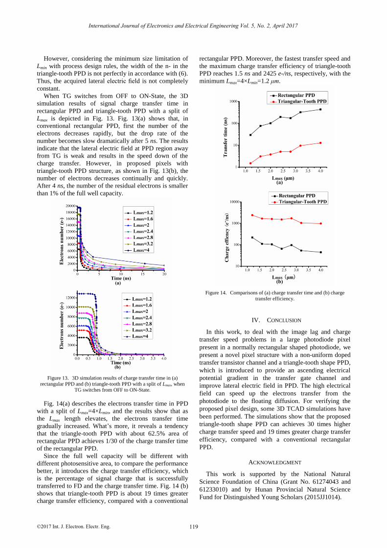
Fig. 14(a) describes the electrons transfer time in PPD
with a split of Lmax=4×Lmin, and the results show that as
the Lmax length elevates, the electrons transfer time
gradually increased. What’s more, it reveals a tendency
that the triangle-tooth PPD with about 62.5% area of
rectangular PPD achieves 1/30 of the charge transfer time
of the rectangular PPD.
Since the full well capacity will be different with
different photosensitive area, to compare the performance
better, it introduces the charge transfer efficiency, which
is the percentage of signal charge that is successfully
transferred to FD and the charge transfer time. Fig. 14 (b)
shows that triangle-tooth PPD is about 19 times greater
charge transfer efficiency, compared with a conventional
rectangular PPD. Moreover, the fastest transfer speed and
the maximum charge transfer efficiency of triangle-tooth
PPD reaches 1.5 ns and 2425 e-/ns, respectively, with the
minimum Lmax=4×Lmin=1.2 μm.
Figure 14. Comparisons of (a) charge transfer time and (b) charge transfer efficiency.
IV. CONCLUSION
In this work, to deal with the image lag and charge
transfer speed problems in a large photodiode pixel
present in a normally rectangular shaped photodiode, we
present a novel pixel structure with a non-uniform doped
transfer transistor channel and a triangle-tooth shape PPD,
which is introduced to provide an ascending electrical
potential gradient in the transfer gate channel and
improve lateral electric field in PPD. The high electrical
field can speed up the electrons transfer from the
photodiode to the floating diffusion. For verifying the
proposed pixel design, some 3D TCAD simulations have
been performed. The simulations show that the proposed
triangle-tooth shape PPD can achieves 30 times higher
charge transfer speed and 19 times greater charge transfer
efficiency, compared with a conventional rectangular
PPD.
ACKNOWLEDGMENT
This work is supported by the National Natural
Science Foundation of China (Grant No. 61274043 and
61233010) and by Hunan Provincial Natural Science
Fund for Distinguished Young Scholars (2015JJ1014).
International Journal of Electronics and Electrical Engineering Vol. 5, No. 2, April 2017
©2017 Int. J. Electron. Electr. Eng. 119

REFERENCES
[1] X. Liu, et al., “High performance CMOS image sensor for low light imaging,” in Proc. International Image Sensor Workshop,
2007, pp. 327–330. [2]
imaging,” in Proc. International Conference on Solid State
Devices and Materials, 2013, pp. 872-873. [3] I. Inoue, et al., “Low-leakage-current and low-operating-voltage
buried photodiode for a CMOS imager,” IEEE Transactions on Electron Devices, vol. 50, no. 1, pp. 43–47, 2003.
[4] R. K. Janval, D. Misra, and J. L. Lowrance, “Charge transfer in a
multi-implant pinned-buried photodetector,” IEEE Transactions on Electron Devices, vol. 48, no. 5, pp. 858-862, 2001.
[5] K. Yonemoto and H. Sumi, “A CMOS image sensor with a simple fixed-pattern-noise-reduction technology and a hole accumulation
diode,” IEEE Journal of Solid-State Circuits, vol. 35, no. 12, pp.
2038-2043, 2000. [6] H. Ihara, “Peninsula transfer gate in a CMOS pixel,” U.S. Patent
12/641, 133, Dec. 17, 2009. [7] H. Takeshita, et al., “High-speed charge transfer pinned-
photodiode for a CMOS time-of-flight range image sensor,”
Proceedings of SPIE, Jan. 2010. [8] J. Yu, et al., “Two–dimensional pixel image lag simulation and
optimization in a 4–T CMOS image sensor,” Journal of Semiconductors, vol. 31, no. 9, pp. 094011–1–094011–5, 2010.
[9] B. Shin, S. Park, and H Shin, “The effect of photodiode shape on
charge transfer in CMOS image sensors,” Solid-State Electronics, vol. 54, no. 11, pp. 1416-1420, 2010.
[10] C. Tubert, et al., “High speed dual port pinned-photodiode for time-of-flight imaging,” in Proc. International Image Sensor
Workshop, 2009.
[11] S. M. Sze, Physics of Semiconductor Devices, New York: Wiley,
[12] K. Miyauchi, et al., “Pixel structure with 10 nsec fully charge
transfer time for the 20M frame per second burst CMOS image
sensor,” Proceedings of SPIE, pp. 902203-1-902203-12, 2014.
Weihui Liu was born in Hunan province, China, in 1990, received the B.S. degree from
School of Physics and Optoelectronics,
Xiangtan University, in 2013. He is currently working towards the M.S. degree in School of
Physics and Optoelectronics, Xiangtan University. His research interests include
CMOS image sensor design and high-speed
pixel design.
Xiangliang Jin received the M.S. degree in
micro technology with emphasis in electric circuits from Hunan University in 2000. He
received the PhD degree in micro-electronics and solid-state circuits with emphasis in
CMOS image sensor design from institute of
microelectronics of Chinese academy of sciences in March 2004. After graduation, he
sets up Superpix Micro technology Ltd. as one co-founder. He is currently a professor in
Xiangtan University. His interests include MEMS and readout circuit
design, CMOS image sensor design, and mixed-mode application-specific integrated circuits with emphasis on high-performance imaging.
Hongjiao Yang is currently pursuing her M.D. degree in School of
Physics and Optoelectronics, Xiangtan University. Her research
interests included single photon avalanche diode (SPAD) design.
Lizhen Tang is currently pursuing her M.S. degree in School of Physics and Optoelectronics, Xiangtan University. Her research interests
included time-to-digital converter (TDC) design.
Jia Yang is currently pursuing his M.S. degree in School of Physics and
Optoelectronics, Xiangtan University. His research interests included single photon avalanche diode (SPAD) design.
International Journal of Electronics and Electrical Engineering Vol. 5, No. 2, April 2017
©2017 Int. J. Electron. Electr. Eng. 120
1981, pp. 77-80.
R. Kuroda, et al., “Ultra-high speed image sensors for scientific