Embed Size (px)
Citation preview
Journal of Physics D: Applied Physics
PAPER
Design of Schottky barrier for plasmon-induced hot-electron passivationof defect environments of semiconductor quantum dotsTo cite this article: Seyed M Sadeghi et al 2020 J. Phys. D: Appl. Phys. 53 115103
View the article online for updates and enhancements.
This content was downloaded from IP address 129.237.90.147 on 13/01/2020 at 18:05
1 © 2020 IOP Publishing Ltd Printed in the UK
1. Introduction
The primary mechanism behind plasmonic enhancement of emission of semiconductor quantum dots (QDs) is reduction of their radiative lifetimes via near fields of metallic nano-structures [1–6]. This process (Purcell effect) makes the radia-tive decay process of QDs more competitive compared to their non-radiative decay channels, allowing the excitation energy
to be more efficiently diverted towards emission of photons. The non-radiative decay processes in QDs are mostly due to the exposure of excitons to a wide range of surface-states and trap sites (defect environments), leading to entrapment of charges and enhancement of Auger recombination (figure 1(a)) [7–9]. Some of the excitation energy is also directly transferred to the metallic nanostructures via Forster reso-nance energy transfer (FRET). Therefore, the presence of
Journal of Physics D: Applied Physics
Design of Schottky barrier for plasmon-induced hot-electron passivation of defect environments of semiconductor quantum dots
Seyed M Sadeghi1,2 , Rithvik R Gutha1 , Jamie S Wilt3 and Judy Z Wu3
1 Department of Physics and Astronomy, University of Alabama in Huntsville, Huntsville, AL 35899, United States of America2 Nano and Micro Device Center, University of Alabama in Huntsville, Huntsville, AL 35899, United States of America3 Department of Physics and Astronomy, University of Kansas, Lawrence, KS 66045, United States of America
E-mail: [email protected]
Received 21 August 2019, revised 25 November 2019Accepted for publication 12 December 2019Published 3 January 2020
AbstractMetal oxide plasmonic metafilms consisting of a Au/Si Schottky barrier in close vicinity of a Si/Al oxide charge barrier can suppress defect-induced non-radiative decay rates of semiconductor quantum dots, enhancing their emission efficiency beyond what the near field enhancement of metallic nanostructures (Purcell effect) can offer (Sadeghi et al 2017 Nanotechnology 29 015402). In this paper we study the impact of the efficiency of the hot electron transfer across the Schottky barrier on such plasmon-induced suppression of the impact of the defect environments. For this the emission intensity and dynamics of quantum dots on such metafilms are studied as the structural features of the Schottky barrier are controlled. We consider the Si layer that separates the Schottky barrier from the charge barrier is either intrinsically undoped, p-doped, or n-doped. Our results show the metafilms with n-type Si can elongate the emission lifetime of the quantum dots the most, suggesting a superior quarantine of excitons against the defect environments. This highlights the fact that n-type Schottky barriers can more efficiently capture the hot electrons generated via non-radiative decay of plasmons. This allows an improved plasmon-induced screening of the excitons against the defect environment.
Keywords: semiconductor quantum dots, plasmons, metafilms, metal oxide, Schottky junction, ultrahigh emission enhancement, excitons
(Some figures may appear in colour only in the online journal)
S M Sadeghi et al
Design of Schottky barrier for plasmon-induced hot-electron passivation of defect environments of semiconductor quantum dots
Printed in the UK
115103
JPAPBE
© 2020 IOP Publishing Ltd
53
J. Phys. D: Appl. Phys.
JPD
10.1088/1361-6463/ab6146
Paper
11
Journal of Physics D: Applied Physics
IOP
2020
1361-6463
1361-6463/ 20 /115103+7$33.00
https://doi.org/10.1088/1361-6463/ab6146J. Phys. D: Appl. Phys. 53 (2020) 115103 (7pp)
S M Sadeghi et al
2
plasmonic nanocavities, nanopatch antennas, and plasmonic gap modes does not alter the defect environments (DEs) of QDs, but rather remedy their impact [10–14].
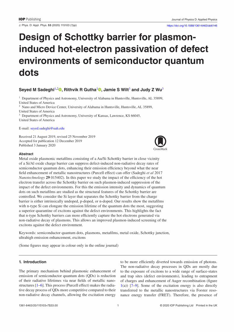
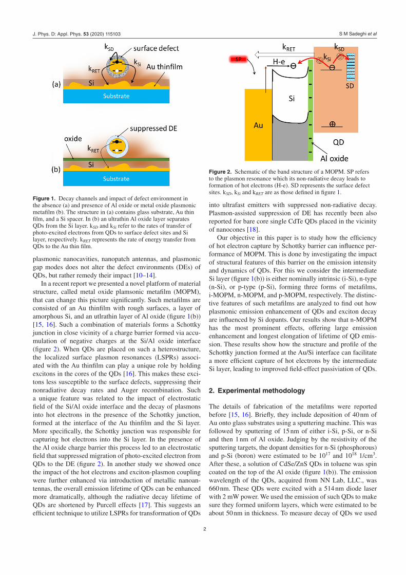
In a recent report we presented a novel platform of material structure, called metal oxide plamsonic metafilm (MOPM), that can change this picture significantly. Such metafilms are consisted of an Au thinfilm with rough surfaces, a layer of amorphous Si, and an utlrathin layer of Al oxide (figure 1(b)) [15, 16]. Such a combination of materials forms a Schottky junction in close vicinity of a charge barrier formed via accu-mulation of negative charges at the Si/Al oxide interface (figure 2). When QDs are placed on such a heterostructure, the localized surface plasmon resonances (LSPRs) associ-ated with the Au thinfilm can play a unique role by holding excitons in the cores of the QDs [16]. This makes these exci-tons less susceptible to the surface defects, suppressing their nonradiative decay rates and Auger recombination. Such a unique feature was related to the impact of electrostatic field of the Si/Al oxide interface and the decay of plasmons into hot electrons in the presence of the Schottky junction, formed at the interface of the Au thinfilm and the Si layer. More specifically, the Schottky junction was responsible for capturing hot electrons into the Si layer. In the presence of the Al oxide charge barrier this process led to an electrostatic field that suppressed migration of photo-excited electron from QDs to the DE (figure 2). In another study we showed once the impact of the hot electrons and exciton-plasmon coupling were further enhanced via introduction of metallic nanoan-tennas, the overall emission lifetime of QDs can be enhanced more dramatically, although the radiative decay lifetime of QDs are shortened by Purcell effects [17]. This suggests an efficient technique to utilize LSPRs for transformation of QDs
into ultrafast emitters with suppressed non-radiative decay. Plasmon-assisted suppression of DE has recently been also reported for bare core single CdTe QDs placed in the vicinity of nanocones [18].
Our objective in this paper is to study how the efficiency of hot electron capture by Schottky barrier can influence per-formance of MOPM. This is done by investigating the impact of structural features of this barrier on the emission intensity and dynamics of QDs. For this we consider the intermediate Si layer (figure 1(b)) is either nominally intrinsic (i-Si), n-type (n-Si), or p-type (p-Si), forming three forms of metafilms, i-MOPM, n-MOPM, and p-MOPM, respectively. The distinc-tive features of such metafilms are analyzed to find out how plasmonic emission enhancement of QDs and exciton decay are influenced by Si dopants. Our results show that n-MOPM has the most prominent effects, offering large emission enhancement and longest elongation of lifetime of QD emis-sion. These results show how the structure and profile of the Schottky junction formed at the Au/Si interface can facilitate a more efficient capture of hot electrons by the intermediate Si layer, leading to improved field-effect passiviation of QDs.
2. Experimental methodology
The details of fabrication of the metafilms were reported before [15, 16]. Briefly, they include deposition of 40 nm of Au onto glass substrates using a sputtering machine. This was followed by sputtering of 15 nm of either i-Si, p-Si, or n-Si and then 1 nm of Al oxide. Judging by the resistivity of the sputtering targets, the dopant densities for n-Si (phosphorous) and p-Si (boron) were estimated to be 1017 and 1018 1/cm3. After these, a solution of CdSe/ZnS QDs in toluene was spin coated on the top of the Al oxide (figure 1(b)). The emission wavelength of the QDs, acquired from NN Lab, LLC., was 660 nm. These QDs were excited with a 514 nm diode laser with 2 mW power. We used the emission of such QDs to make sure they formed uniform layers, which were estimated to be about 50 nm in thickness. To measure decay of QDs we used
Figure 1. Decay channels and impact of defect environment in the absence (a) and presence of Al oxide or metal oxide plasmonic metafilm (b). The structure in (a) contains glass substrate, Au thin film, and a Si spacer. In (b) an ultrathin Al oxide layer separates QDs from the Si layer. kSD and kSi refer to the rates of transfer of photo-excited electrons from QDs to surface defect sites and Si layer, respectively. kRET represents the rate of energy transfer from QDs to the Au thin film.
Figure 2. Schematic of the band structure of a MOPM. SP refers to the plasmon resonance which its non-radiative decay leads to formation of hot electrons (H-e). SD represents the surface defect sites. kSD, kSi and kRET are as those defined in figure 1.
J. Phys. D: Appl. Phys. 53 (2020) 115103
S M Sadeghi et al
3
a time correlated single photon counting (TCSPC) system (Picoquant Pico-Timeharp 260) combined with a 30 ps pulsed laser with 450 nm wavelength.
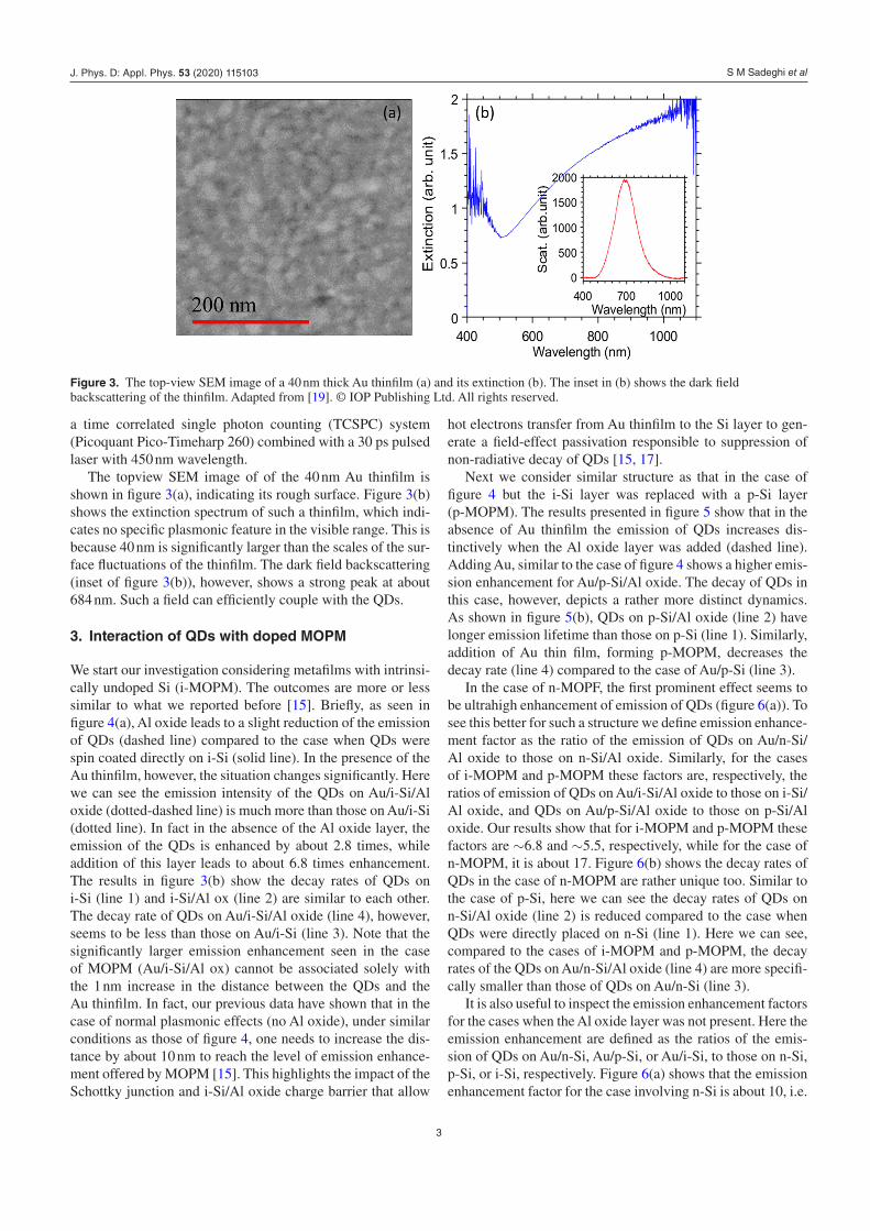
The topview SEM image of of the 40 nm Au thinfilm is shown in figure 3(a), indicating its rough surface. Figure 3(b) shows the extinction spectrum of such a thinfilm, which indi-cates no specific plasmonic feature in the visible range. This is because 40 nm is significantly larger than the scales of the sur-face fluctuations of the thinfilm. The dark field backscattering (inset of figure 3(b)), however, shows a strong peak at about 684 nm. Such a field can efficiently couple with the QDs.
3. Interaction of QDs with doped MOPM
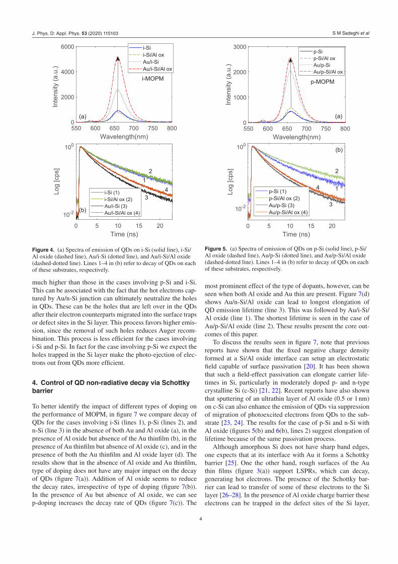
We start our investigation considering metafilms with intrinsi-cally undoped Si (i-MOPM). The outcomes are more or less similar to what we reported before [15]. Briefly, as seen in figure 4(a), Al oxide leads to a slight reduction of the emission of QDs (dashed line) compared to the case when QDs were spin coated directly on i-Si (solid line). In the presence of the Au thinfilm, however, the situation changes significantly. Here we can see the emission intensity of the QDs on Au/i-Si/Al oxide (dotted-dashed line) is much more than those on Au/i-Si (dotted line). In fact in the absence of the Al oxide layer, the emission of the QDs is enhanced by about 2.8 times, while addition of this layer leads to about 6.8 times enhancement. The results in figure 3(b) show the decay rates of QDs on i-Si (line 1) and i-Si/Al ox (line 2) are similar to each other. The decay rate of QDs on Au/i-Si/Al oxide (line 4), however, seems to be less than those on Au/i-Si (line 3). Note that the significantly larger emission enhancement seen in the case of MOPM (Au/i-Si/Al ox) cannot be associated solely with the 1 nm increase in the distance between the QDs and the Au thinfilm. In fact, our previous data have shown that in the case of normal plasmonic effects (no Al oxide), under similar conditions as those of figure 4, one needs to increase the dis-tance by about 10 nm to reach the level of emission enhance-ment offered by MOPM [15]. This highlights the impact of the Schottky junction and i-Si/Al oxide charge barrier that allow
hot electrons transfer from Au thinfilm to the Si layer to gen-erate a field-effect passivation responsible to suppression of non-radiative decay of QDs [15, 17].
Next we consider similar structure as that in the case of figure 4 but the i-Si layer was replaced with a p-Si layer (p-MOPM). The results presented in figure 5 show that in the absence of Au thinfilm the emission of QDs increases dis-tinctively when the Al oxide layer was added (dashed line). Adding Au, similar to the case of figure 4 shows a higher emis-sion enhancement for Au/p-Si/Al oxide. The decay of QDs in this case, however, depicts a rather more distinct dynamics. As shown in figure 5(b), QDs on p-Si/Al oxide (line 2) have longer emission lifetime than those on p-Si (line 1). Similarly, addition of Au thin film, forming p-MOPM, decreases the decay rate (line 4) compared to the case of Au/p-Si (line 3).
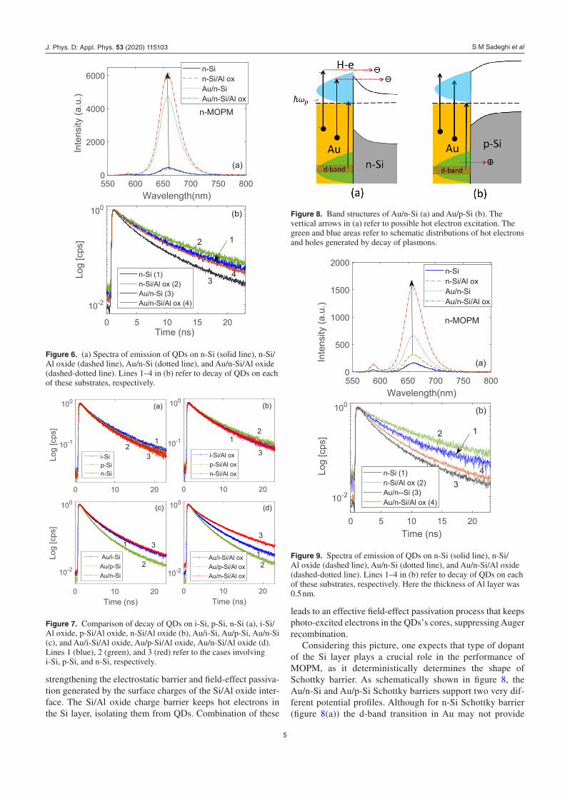
In the case of n-MOPF, the first prominent effect seems to be ultrahigh enhancement of emission of QDs (figure 6(a)). To see this better for such a structure we define emission enhance-ment factor as the ratio of the emission of QDs on Au/n-Si/Al oxide to those on n-Si/Al oxide. Similarly, for the cases of i-MOPM and p-MOPM these factors are, respectively, the ratios of emission of QDs on Au/i-Si/Al oxide to those on i-Si/Al oxide, and QDs on Au/p-Si/Al oxide to those on p-Si/Al oxide. Our results show that for i-MOPM and p-MOPM these factors are ∼6.8 and ∼5.5, respectively, while for the case of n-MOPM, it is about 17. Figure 6(b) shows the decay rates of QDs in the case of n-MOPM are rather unique too. Similar to the case of p-Si, here we can see the decay rates of QDs on n-Si/Al oxide (line 2) is reduced compared to the case when QDs were directly placed on n-Si (line 1). Here we can see, compared to the cases of i-MOPM and p-MOPM, the decay rates of the QDs on Au/n-Si/Al oxide (line 4) are more specifi-cally smaller than those of QDs on Au/n-Si (line 3).
It is also useful to inspect the emission enhancement factors for the cases when the Al oxide layer was not present. Here the emission enhancement are defined as the ratios of the emis-sion of QDs on Au/n-Si, Au/p-Si, or Au/i-Si, to those on n-Si, p-Si, or i-Si, respectively. Figure 6(a) shows that the emission enhancement factor for the case involving n-Si is about 10, i.e.
Figure 3. The top-view SEM image of a 40 nm thick Au thinfilm (a) and its extinction (b). The inset in (b) shows the dark field backscattering of the thinfilm. Adapted from [19]. © IOP Publishing Ltd. All rights reserved.
J. Phys. D: Appl. Phys. 53 (2020) 115103
S M Sadeghi et al
4
much higher than those in the cases involving p-Si and i-Si. This can be associated with the fact that the hot electrons cap-tured by Au/n-Si junction can ultimately neutralize the holes in QDs. These can be the holes that are left over in the QDs after their electron counterparts migrated into the surface traps or defect sites in the Si layer. This process favors higher emis-sion, since the removal of such holes reduces Auger recom-bination. This process is less efficient for the cases involving i-Si and p-Si. In fact for the case involving p-Si we expect the holes trapped in the Si layer make the photo-ejection of elec-trons out from QDs more efficient.
4. Control of QD non-radiative decay via Schottky barrier
To better identify the impact of different types of doping on the performance of MOPM, in figure 7 we compare decay of QDs for the cases involving i-Si (lines 1), p-Si (lines 2), and n-Si (line 3) in the absence of both Au and Al oxide (a), in the presence of Al oxide but absence of the Au thinfilm (b), in the presence of Au thinfilm but absence of Al oxide (c), and in the presence of both the Au thinfilm and Al oxide layer (d). The results show that in the absence of Al oxide and Au thinfilm, type of doping does not have any major impact on the decay of QDs (figure 7(a)). Addition of Al oxide seems to reduce the decay rates, irrespective of type of doping (figure 7(b)). In the presence of Au but absence of Al oxide, we can see p-doping increases the decay rate of QDs (figure 7(c)). The
most prominent effect of the type of dopants, however, can be seen when both Al oxide and Au thin are present. Figure 7(d) shows Au/n-Si/Al oxide can lead to longest elongation of QD emission lifetime (line 3). This was followed by Au/i-Si/Al oxide (line 1). The shortest lifetime is seen in the case of Au/p-Si/Al oxide (line 2). These results present the core out-comes of this paper.
To discuss the results seen in figure 7, note that previous reports have shown that the fixed negative charge density formed at a Si/Al oxide interface can setup an electrostatic field capable of surface passivation [20]. It has been shown that such a field-effect passivation can elongate carrier life-times in Si, particularly in moderately doped p- and n-type crystalline Si (c-Si) [21, 22]. Recent reports have also shown that sputtering of an ultrathin layer of Al oxide (0.5 or 1 nm) on c-Si can also enhance the emission of QDs via suppression of migration of photoexcited electrons from QDs to the sub-strate [23, 24]. The results for the case of p-Si and n-Si with Al oxide (figures 5(b) and 6(b), lines 2) suggest elongation of lifetime because of the same passivation process.
Although amorphous Si does not have sharp band edges, one expects that at its interface with Au it forms a Schottky barrier [25]. One the other hand, rough surfaces of the Au thin films (figure 3(a)) support LSPRs, which can decay, generating hot electrons. The presence of the Schottky bar-rier can lead to transfer of some of these electrons to the Si layer [26–28]. In the presence of Al oxide charge barrier these electrons can be trapped in the defect sites of the Si layer,
550 600 650 700 750 800Wavelength(nm)
0
2000
4000
6000In
tens
ity (a
.u.)
i-Sii-Si/Al oxAu/i-SiAu/i-Si/Al ox
0 5 10 15 20Time (ns)
10-2
100
Log
[cps
]
i-Si (1)i-Si/Al ox (2)Au/i-Si (3)Au/i-Si/Al ox (4)(b)
21
43
(a)
i-MOPM
Figure 4. (a) Spectra of emission of QDs on i-Si (solid line), i-Si/Al oxide (dashed line), Au/i-Si (dotted line), and Au/i-Si/Al oxide (dashed-dotted line). Lines 1–4 in (b) refer to decay of QDs on each of these substrates, respectively.
550 600 650 700 750 800Wavelength(nm)
0
1000
2000
3000
Inte
nsity
(a.u
.)
p-Sip-Si/Al oxAu/p-SiAu/p-Si/Al ox
0 5 10 15 20Time (ns)
10-2
100
Log
[cps
]
p-Si (1)p-Si/Al ox (2)Au/p-Si (3)Au/p-Si/Al ox (4)
p-MOPM
4 1
2
3
(a)
(b)
Figure 5. (a) Spectra of emission of QDs on p-Si (solid line), p-Si/Al oxide (dashed line), Au/p-Si (dotted line), and Au/p-Si/Al oxide (dashed-dotted line). Lines 1–4 in (b) refer to decay of QDs on each of these substrates, respectively.
J. Phys. D: Appl. Phys. 53 (2020) 115103
S M Sadeghi et al
5
strengthening the electrostatic barrier and field-effect passiva-tion generated by the surface charges of the Si/Al oxide inter-face. The Si/Al oxide charge barrier keeps hot electrons in the Si layer, isolating them from QDs. Combination of these
leads to an effective field-effect passivation process that keeps photo-excited electrons in the QDs’s cores, suppressing Auger recombination.
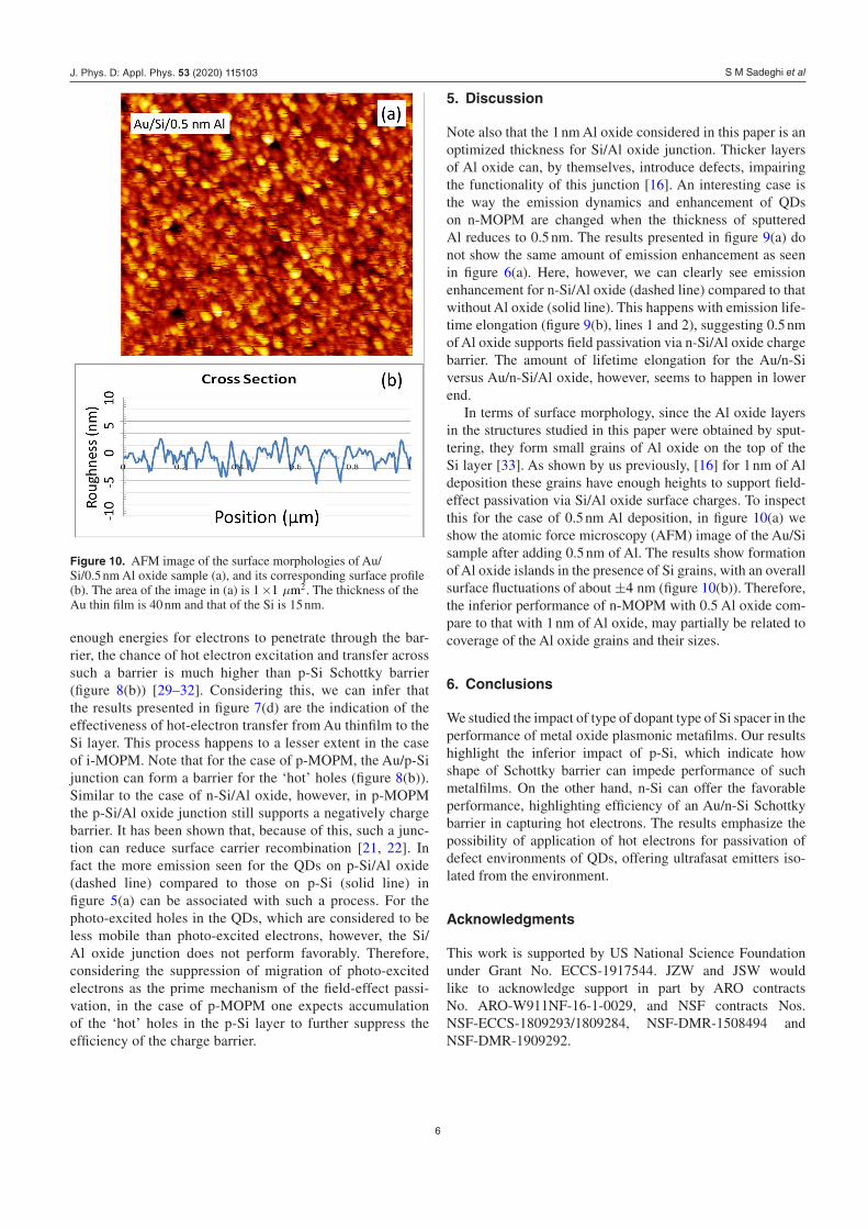
Considering this picture, one expects that type of dopant of the Si layer plays a crucial role in the performance of MOPM, as it deterministically determines the shape of Schottky barrier. As schematically shown in figure 8, the Au/n-Si and Au/p-Si Schottky barriers support two very dif-ferent potential profiles. Although for n-Si Schottky barrier (figure 8(a)) the d-band transition in Au may not provide
550 600 650 700 750 800Wavelength(nm)
0
2000
4000
6000In
tens
ity (a
.u.)
n-Sin-Si/Al oxAu/n-SiAu/n-Si/Al ox
0 5 10 15 20Time (ns)
10-2
100
Log
[cps
]
n-Si (1)n-Si/Al ox (2)Au/n-Si (3)Au/n-Si/Al ox (4)
12
43
n-MOPM
(a)
(b)
Figure 6. (a) Spectra of emission of QDs on n-Si (solid line), n-Si/Al oxide (dashed line), Au/n-Si (dotted line), and Au/n-Si/Al oxide (dashed-dotted line). Lines 1–4 in (b) refer to decay of QDs on each of these substrates, respectively.
0 10 20
10-1
100
Log
[cps
]
i-Sip-Sin-Si
0 10 20
10-1
100
i-Si/Al oxp-Si/Al oxn-Si/Al ox
0 10 20Time (ns)
10-2
100
Log
[cps
]
Au/i-SiAu/p-SiAu/n-Si
0 10 20Time (ns)
10-2
100
Au/i-Si/Al oxAu/p-Si/Al oxAu/n-Si/Al ox
1
3
(a) (b)
(c) (d)
1
3
21
23
21
3
2
Figure 7. Comparison of decay of QDs on i-Si, p-Si, n-Si (a), i-Si/Al oxide, p-Si/Al oxide, n-Si/Al oxide (b), Au/i-Si, Au/p-Si, Au/n-Si (c), and Au/i-Si/Al oxide, Au/p-Si/Al oxide, Au/n-Si/Al oxide (d). Lines 1 (blue), 2 (green), and 3 (red) refer to the cases involving i-Si, p-Si, and n-Si, respectively.
Figure 8. Band structures of Au/n-Si (a) and Au/p-Si (b). The vertical arrows in (a) refer to possible hot electron excitation. The green and blue areas refer to schematic distributions of hot electrons and holes generated by decay of plasmons.
550 600 650 700 750 800Wavelength(nm)
0
500
1000
1500
2000
Inte
nsity
(a.u
.)
n-Sin-Si/Al oxAu/n-SiAu/n-Si/Al ox
0 5 10 15 20Time (ns)
10-2
100
Log
[cps
]
n-Si (1)n-Si/Al ox (2)Au/n--Si (3)Au/n-Si/Al ox (4)
n-MOPM
4
12
3
(b)
(a)
Figure 9. Spectra of emission of QDs on n-Si (solid line), n-Si/Al oxide (dashed line), Au/n-Si (dotted line), and Au/n-Si/Al oxide (dashed-dotted line). Lines 1–4 in (b) refer to decay of QDs on each of these substrates, respectively. Here the thickness of Al layer was 0.5 nm.
J. Phys. D: Appl. Phys. 53 (2020) 115103
S M Sadeghi et al
6
enough energies for electrons to penetrate through the bar-rier, the chance of hot electron excitation and transfer across such a barrier is much higher than p-Si Schottky barrier (figure 8(b)) [29–32]. Considering this, we can infer that the results presented in figure 7(d) are the indication of the effectiveness of hot-electron transfer from Au thinfilm to the Si layer. This process happens to a lesser extent in the case of i-MOPM. Note that for the case of p-MOPM, the Au/p-Si junction can form a barrier for the ‘hot’ holes (figure 8(b)). Similar to the case of n-Si/Al oxide, however, in p-MOPM the p-Si/Al oxide junction still supports a negatively charge barrier. It has been shown that, because of this, such a junc-tion can reduce surface carrier recombination [21, 22]. In fact the more emission seen for the QDs on p-Si/Al oxide (dashed line) compared to those on p-Si (solid line) in figure 5(a) can be associated with such a process. For the photo-excited holes in the QDs, which are considered to be less mobile than photo-excited electrons, however, the Si/Al oxide junction does not perform favorably. Therefore, considering the suppression of migration of photo-excited electrons as the prime mechanism of the field-effect passi-vation, in the case of p-MOPM one expects accumulation of the ‘hot’ holes in the p-Si layer to further suppress the efficiency of the charge barrier.
5. Discussion
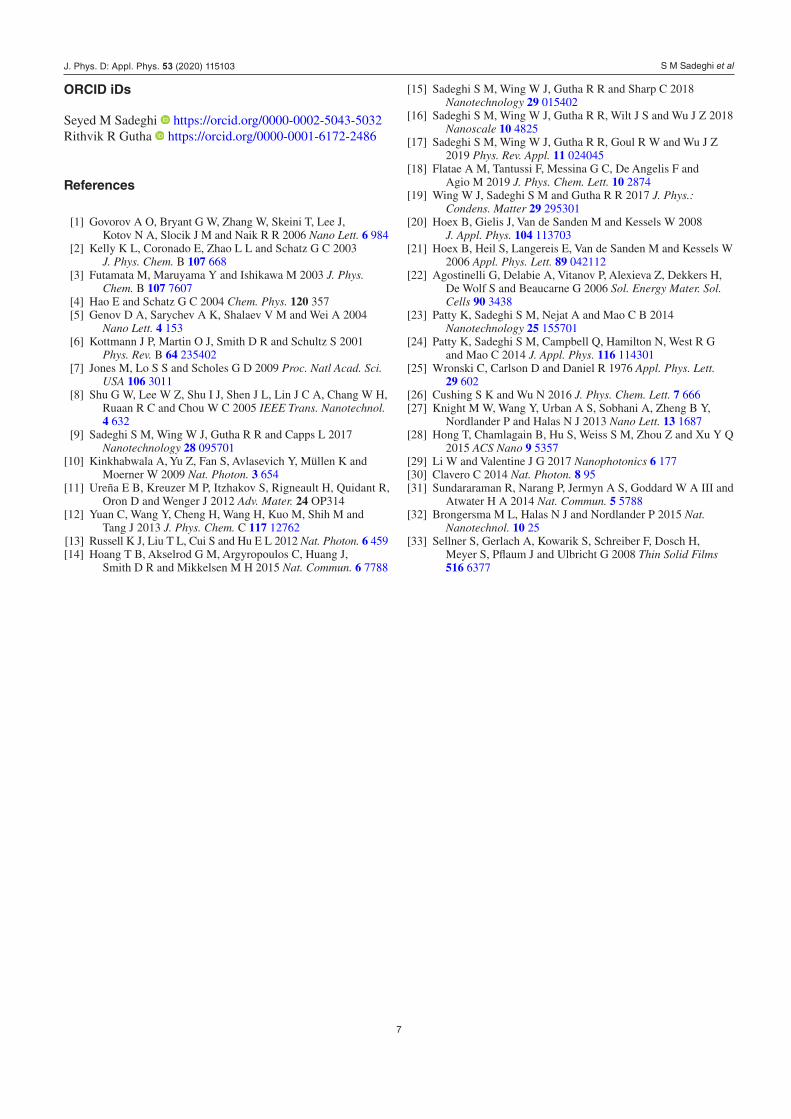
Note also that the 1 nm Al oxide considered in this paper is an optimized thickness for Si/Al oxide junction. Thicker layers of Al oxide can, by themselves, introduce defects, impairing the functionality of this junction [16]. An interesting case is the way the emission dynamics and enhancement of QDs on n-MOPM are changed when the thickness of sputtered Al reduces to 0.5 nm. The results presented in figure 9(a) do not show the same amount of emission enhancement as seen in figure 6(a). Here, however, we can clearly see emission enhancement for n-Si/Al oxide (dashed line) compared to that without Al oxide (solid line). This happens with emission life-time elongation (figure 9(b), lines 1 and 2), suggesting 0.5 nm of Al oxide supports field passivation via n-Si/Al oxide charge barrier. The amount of lifetime elongation for the Au/n-Si versus Au/n-Si/Al oxide, however, seems to happen in lower end.
In terms of surface morphology, since the Al oxide layers in the structures studied in this paper were obtained by sput-tering, they form small grains of Al oxide on the top of the Si layer [33]. As shown by us previously, [16] for 1 nm of Al deposition these grains have enough heights to support field-effect passivation via Si/Al oxide surface charges. To inspect this for the case of 0.5 nm Al deposition, in figure 10(a) we show the atomic force microscopy (AFM) image of the Au/Si sample after adding 0.5 nm of Al. The results show formation of Al oxide islands in the presence of Si grains, with an overall surface fluctuations of about ±4 nm (figure 10(b)). Therefore, the inferior performance of n-MOPM with 0.5 Al oxide com-pare to that with 1 nm of Al oxide, may partially be related to coverage of the Al oxide grains and their sizes.
6. Conclusions
We studied the impact of type of dopant type of Si spacer in the performance of metal oxide plasmonic metafilms. Our results highlight the inferior impact of p-Si, which indicate how shape of Schottky barrier can impede performance of such metalfilms. On the other hand, n-Si can offer the favorable performance, highlighting efficiency of an Au/n-Si Schottky barrier in capturing hot electrons. The results emphasize the possibility of application of hot electrons for passivation of defect environments of QDs, offering ultrafasat emitters iso-lated from the environment.
Acknowledgments
This work is supported by US National Science Foundation under Grant No. ECCS-1917544. JZW and JSW would like to acknowledge support in part by ARO contracts No. ARO-W911NF-16-1-0029, and NSF contracts Nos. NSF-ECCS-1809293/1809284, NSF-DMR-1508494 and NSF-DMR-1909292.
Figure 10. AFM image of the surface morphologies of Au/Si/0.5 nm Al oxide sample (a), and its corresponding surface profile (b). The area of the image in (a) is 1 ×1 µm2. The thickness of the Au thin film is 40 nm and that of the Si is 15 nm.
J. Phys. D: Appl. Phys. 53 (2020) 115103
S M Sadeghi et al
7
ORCID iDs
Seyed M Sadeghi https://orcid.org/0000-0002-5043-5032Rithvik R Gutha https://orcid.org/0000-0001-6172-2486
References
[1] Govorov A O, Bryant G W, Zhang W, Skeini T, Lee J, Kotov N A, Slocik J M and Naik R R 2006 Nano Lett. 6 984
[2] Kelly K L, Coronado E, Zhao L L and Schatz G C 2003 J. Phys. Chem. B 107 668
[3] Futamata M, Maruyama Y and Ishikawa M 2003 J. Phys. Chem. B 107 7607
[4] Hao E and Schatz G C 2004 Chem. Phys. 120 357 [5] Genov D A, Sarychev A K, Shalaev V M and Wei A 2004
Nano Lett. 4 153 [6] Kottmann J P, Martin O J, Smith D R and Schultz S 2001
Phys. Rev. B 64 235402 [7] Jones M, Lo S S and Scholes G D 2009 Proc. Natl Acad. Sci.
USA 106 3011 [8] Shu G W, Lee W Z, Shu I J, Shen J L, Lin J C A, Chang W H,
Ruaan R C and Chou W C 2005 IEEE Trans. Nanotechnol. 4 632
[9] Sadeghi S M, Wing W J, Gutha R R and Capps L 2017 Nanotechnology 28 095701
[10] Kinkhabwala A, Yu Z, Fan S, Avlasevich Y, Müllen K and Moerner W 2009 Nat. Photon. 3 654
[11] Ureña E B, Kreuzer M P, Itzhakov S, Rigneault H, Quidant R, Oron D and Wenger J 2012 Adv. Mater. 24 OP314
[12] Yuan C, Wang Y, Cheng H, Wang H, Kuo M, Shih M and Tang J 2013 J. Phys. Chem. C 117 12762
[13] Russell K J, Liu T L, Cui S and Hu E L 2012 Nat. Photon. 6 459[14] Hoang T B, Akselrod G M, Argyropoulos C, Huang J,
Smith D R and Mikkelsen M H 2015 Nat. Commun. 6 7788
[15] Sadeghi S M, Wing W J, Gutha R R and Sharp C 2018 Nanotechnology 29 015402
[16] Sadeghi S M, Wing W J, Gutha R R, Wilt J S and Wu J Z 2018 Nanoscale 10 4825
[17] Sadeghi S M, Wing W J, Gutha R R, Goul R W and Wu J Z 2019 Phys. Rev. Appl. 11 024045
[18] Flatae A M, Tantussi F, Messina G C, De Angelis F and Agio M 2019 J. Phys. Chem. Lett. 10 2874
[19] Wing W J, Sadeghi S M and Gutha R R 2017 J. Phys.: Condens. Matter 29 295301
[20] Hoex B, Gielis J, Van de Sanden M and Kessels W 2008 J. Appl. Phys. 104 113703
[21] Hoex B, Heil S, Langereis E, Van de Sanden M and Kessels W 2006 Appl. Phys. Lett. 89 042112
[22] Agostinelli G, Delabie A, Vitanov P, Alexieva Z, Dekkers H, De Wolf S and Beaucarne G 2006 Sol. Energy Mater. Sol. Cells 90 3438
[23] Patty K, Sadeghi S M, Nejat A and Mao C B 2014 Nanotechnology 25 155701
[24] Patty K, Sadeghi S M, Campbell Q, Hamilton N, West R G and Mao C 2014 J. Appl. Phys. 116 114301
[25] Wronski C, Carlson D and Daniel R 1976 Appl. Phys. Lett. 29 602
[26] Cushing S K and Wu N 2016 J. Phys. Chem. Lett. 7 666[27] Knight M W, Wang Y, Urban A S, Sobhani A, Zheng B Y,
Nordlander P and Halas N J 2013 Nano Lett. 13 1687[28] Hong T, Chamlagain B, Hu S, Weiss S M, Zhou Z and Xu Y Q
2015 ACS Nano 9 5357[29] Li W and Valentine J G 2017 Nanophotonics 6 177[30] Clavero C 2014 Nat. Photon. 8 95[31] Sundararaman R, Narang P, Jermyn A S, Goddard W A III and
Atwater H A 2014 Nat. Commun. 5 5788[32] Brongersma M L, Halas N J and Nordlander P 2015 Nat.
Nanotechnol. 10 25[33] Sellner S, Gerlach A, Kowarik S, Schreiber F, Dosch H,
Meyer S, Pflaum J and Ulbricht G 2008 Thin Solid Films 516 6377
J. Phys. D: Appl. Phys. 53 (2020) 115103