Embed Size (px)
Citation preview

Design of Standing-Wave Accelerator Structure
Jeff Neilson, Sami Tantawi, and Valery Dolgashev
SLAC National Accelerator Laboratory
US High Gradient Research Collaboration Workshop February 9-10, 2011
Page 2
Outline
• Motivation
• Conceptual Approach
• Feed System Design
• Cavity Design
• Fabrication
• Conclusions
Motivation
• Provide robust high-gradient (>100 MV/m) accelerator structure
• Potential advantages of parallel fed, πmode standing-wave (SW) structures over travelling-wave structures– minimizes energy available during breakdown
– maximizes power distribution efficiency
– enhanced vacuum pumping conductance
– empirical evidence πmode have lower breakdown rate at given gradient vs. travelling wave structures
Page 3

Approach*
• Individually fed π mode cavities
Page 4
RFsource
Directional Coupler Sc = (1 – i + N)-1/2
Accelerator Cavity
Nth Accelerator Cavity
Load
*S. Tantawi,” RF distribution system for a set of standing-wave accelerator structures”, Phys. Rev., ST Accel. Beams,vol. 9, issue 11
Approach - Cont
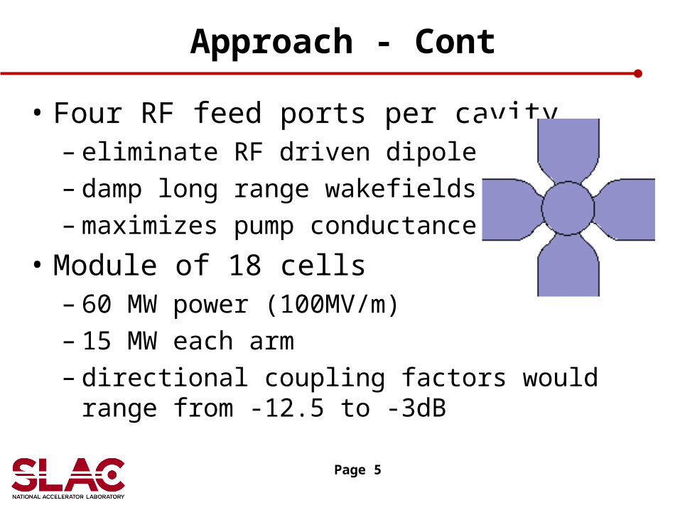
• Four RF feed ports per cavity– eliminate RF driven dipole modes– damp long range wakefields– maximizes pump conductance
• Module of 18 cells – 60 MW power (100MV/m)– 15 MW each arm– directional coupling factors would range from -
12.5 to -3dB
Page 5

Page 6
Coupler Design
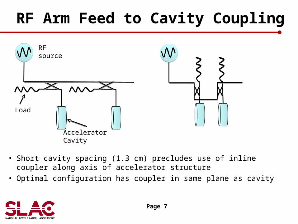
RF Arm Feed to Cavity Coupling
• Short cavity spacing (1.3 cm) precludes use of inline coupler along axis of accelerator structure
• Optimal configuration has coupler in same plane as cavity
Page 7
RFsource
Accelerator Cavity
Load
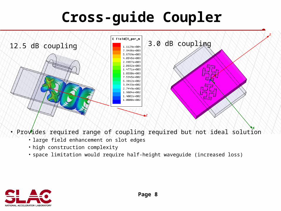
Cross-guide Coupler
Page 8
3.0 dB coupling12.5 dB coupling
• Provides required range of coupling required but not ideal solution• large field enhancement on slot edges• high construction complexity• space limitation would require half-height waveguide (increased loss)
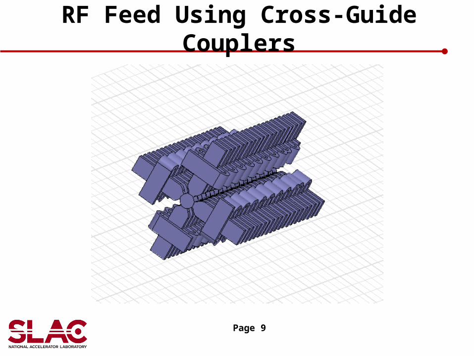
RF Feed Using Cross-Guide Couplers
Page 9

Biplanar Directional Coupler*
• Can be designed for coupling over desired range• Compact, minimal field enhancement• Planar shape – easy to machine
Page 10
*MIT Radiation Laboratory Series, Vol. 8, “Principles of Microwave Circuits”
Electric field for 3dB Coupler

Coupling Sensitivity to Parameter Variation
Page 11
• Variation in coupling will reduce average gradient over structure from optimal value
• Monte Carlo calculation performed varying u, v, d by +/- .0025 cm
• 12.5 dB design has significantly more sensitivity than 3dB design
Coupling Histogram for 12.5 dB DesignTolerance = +/- .0025 cm
vu
d
Coupling Histogram for 3 dB DesignTolerance = +/- .0025 cm
Fre
qu
en
cy o
f O
ccu
rre
nce
Fre
qu
en
cy o
f O
ccu
rre
nce
Difference from Design Value (%) Difference from Design Value (%)
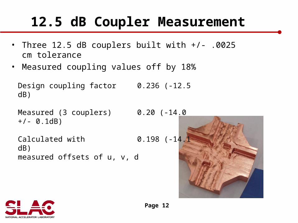
12.5 dB Coupler Measurement
Page 12
Design coupling factor 0.236 (-12.5 dB)
Measured (3 couplers) 0.20 (-14.0 +/- 0.1dB)
Calculated with 0.198 (-14.1 dB)measured offsets of u, v, d
• Three 12.5 dB couplers built with +/- .0025 cm tolerance• Measured coupling values off by 18%
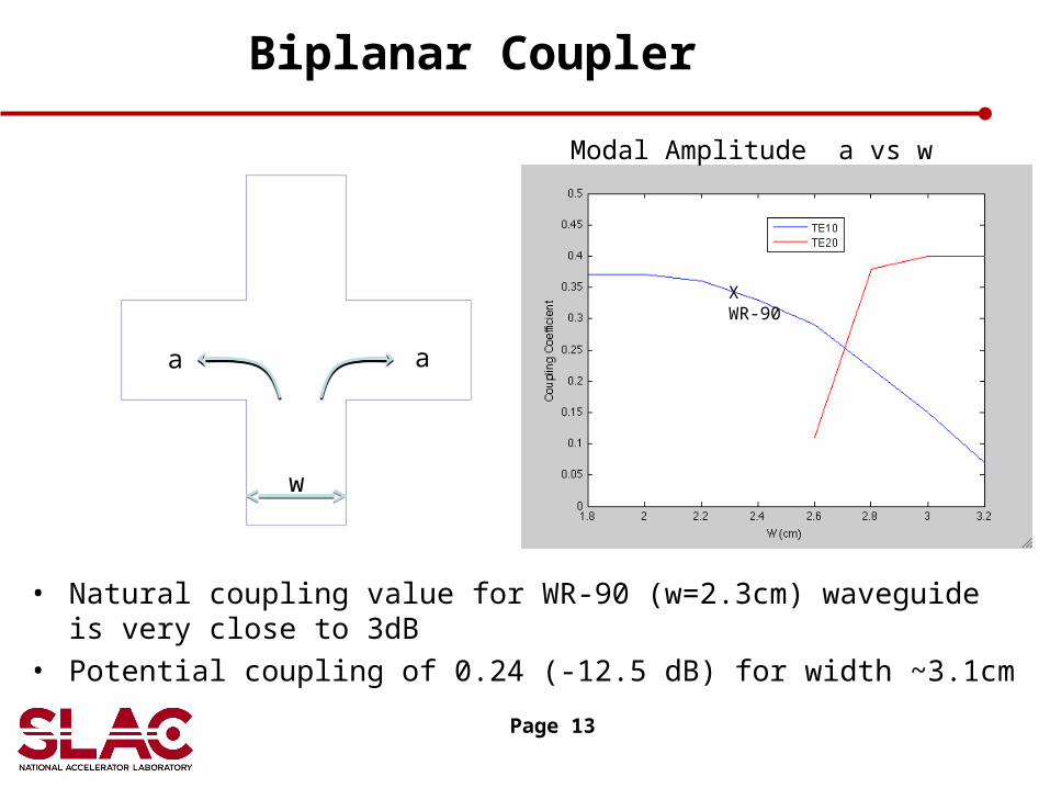
a a
w
• Natural coupling value for WR-90 (w=2.3cm) waveguide is very close to 3dB
• Potential coupling of 0.24 (-12.5 dB) for width ~3.1cm
XWR-90
Modal Amplitude a vs w
Biplanar Coupler
Page 13
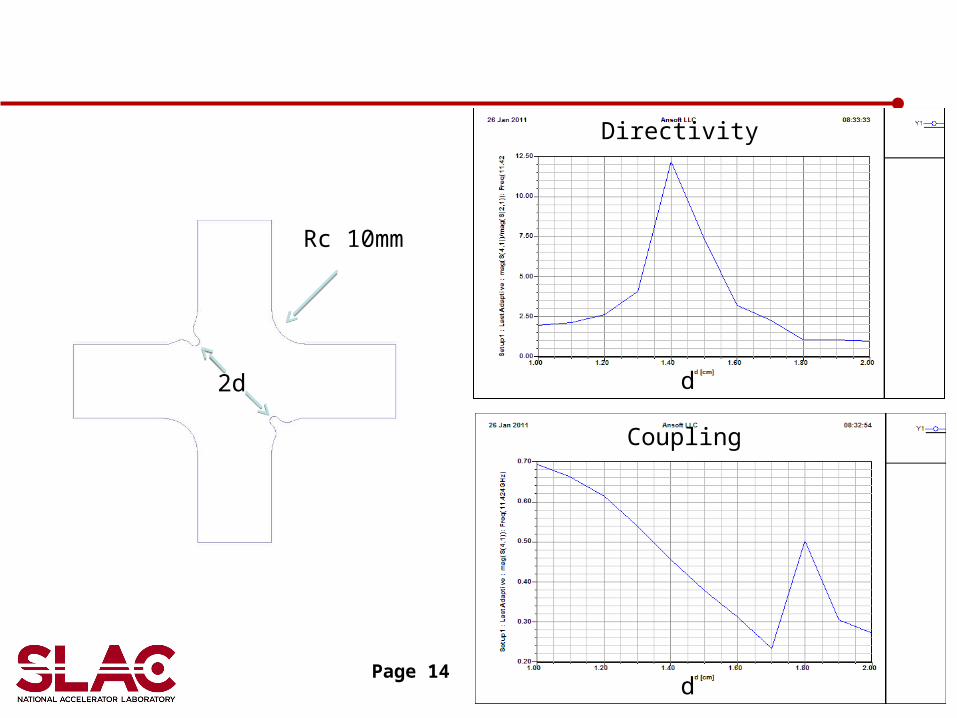
Rc 10mm
Directivity
Coupling
2d d
dPage 14

P 15 MWEmax 17 MV/mHmax 50 kA/m
Rc 10.6mm
Coupling Histogram for 12.5 dB DesignTolerance = +/- .0025 cmVariation u, v, d, and rc
Page 15
Fre
qu
en
cy o
f O
ccu
rre
nce
Difference from Design Value (%)
Improved 12.5 dB Coupler
Page 16
Cavity Design
Cavity Design Goals
• Proof of concept
• Achieved results will determine relevant applications of SW approach
• Nominal goal is CLIC G• acceleration gradient 100 MV/m• iris a/λ 0.11 (average CLIC G)
Page 17
Cavity Design
• Four port coupling designed to provide– rf drive to beam– long range wakefield damping– high pump conductance
• With– Minimal pulse heating and electric field
enhancement– maintain high shunt impedance– minimizing construction complexity
Page 18
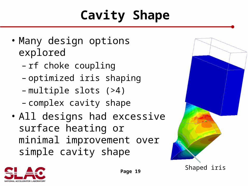
Cavity Shape
• Many design options explored– rf choke coupling– optimized iris shaping– multiple slots (>4)– complex cavity shape
• All designs had excessive surface heating or minimal improvement over simple cavity shape
Page 19Shaped iris
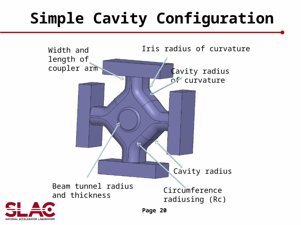
Width and length of coupler arm
Iris radius of curvature
Cavity radius of curvature
Cavity radius
Beam tunnel radius and thickness
Circumference radiusing (Rc)
Simple Cavity Configuration
Page 20
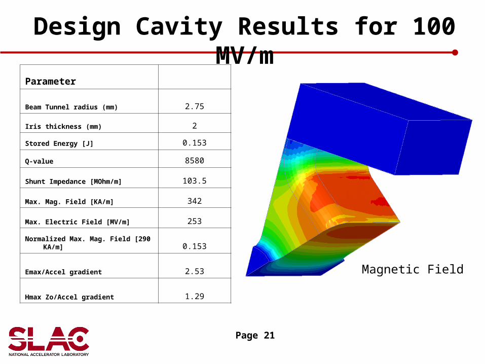
Page 21
Magnetic Field
Parameter
Beam Tunnel radius (mm) 2.75
Iris thickness (mm) 2
Stored Energy [J] 0.153
Q-value 8580
Shunt Impedance [MOhm/m] 103.5
Max. Mag. Field [KA/m] 342
Max. Electric Field [MV/m] 253
Normalized Max. Mag. Field [290 KA/m] 0.153
Emax/Accel gradient 2.53
Hmax Zo/Accel gradient 1.29
Design Cavity Results for 100 MV/m

Fabrication
Page 22
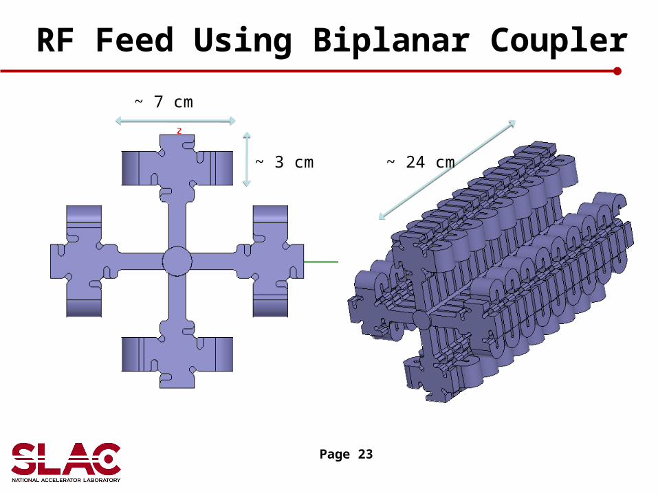
RF Feed Using Biplanar Coupler
Page 23
~ 7 cm
~ 3 cm ~ 24 cm
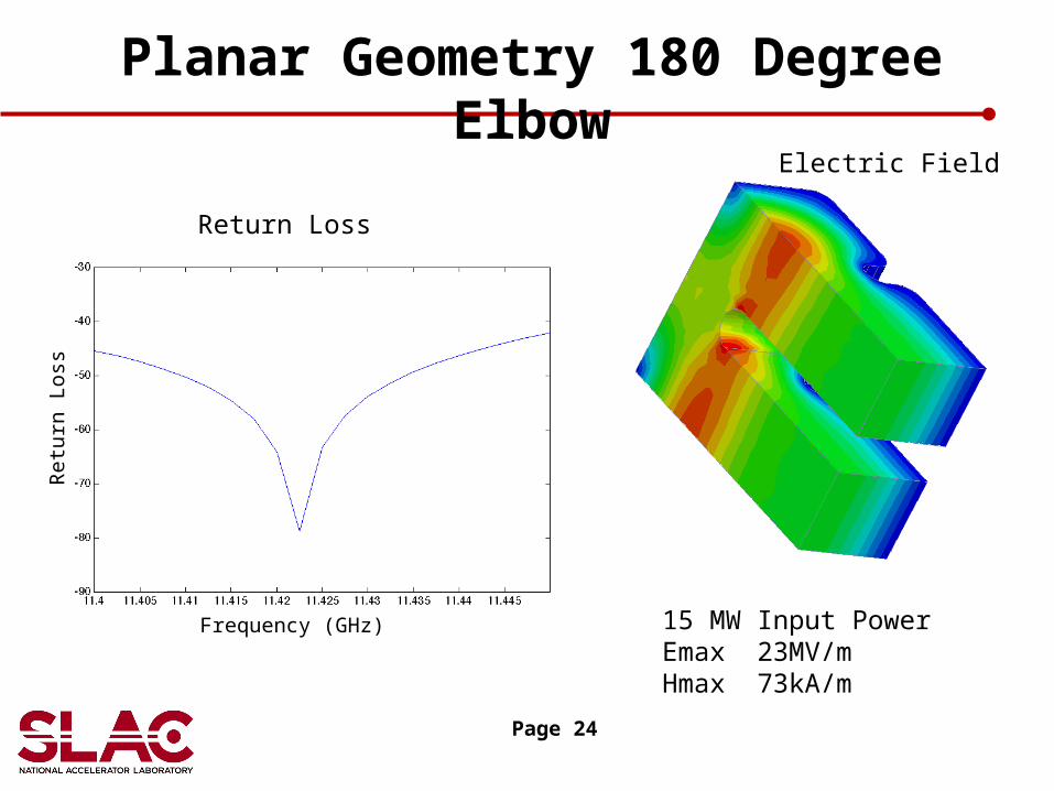
15 MW Input PowerEmax 23MV/mHmax 73kA/m
Return Loss
Page 24
Planar Geometry 180 Degree Elbow
Frequency (GHz)
Ret
urn
Los
s
Electric Field

Page 25
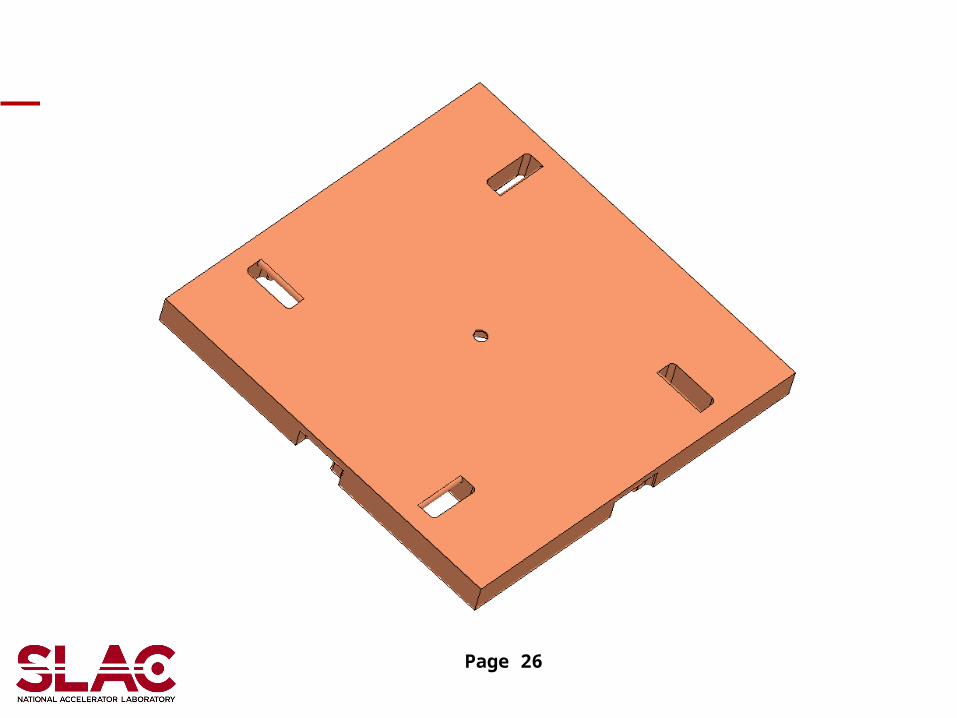
Page 26
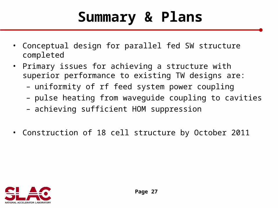
Summary & Plans
• Conceptual design for parallel fed SW structure completed• Primary issues for achieving a structure with superior performance to
existing TW designs are:– uniformity of rf feed system power coupling– pulse heating from waveguide coupling to cavities– achieving sufficient HOM suppression
• Construction of 18 cell structure by October 2011
Page 27