Embed Size (px)
Citation preview
International Journal on Electrical Engineering and Informatics ‐ Volume 7, Number 2, June 2015 Design of Triple-Stage Cascoded LNA Amplifiers using Inductive Drain
Feedback (IDF) Technique for WiMAX Application
Kamil PONGOT1.2, Abdul Rani OTHMAN2, Zahriladha ZAKARIA2, Mohamad Kadim SUAIDI2, Abdul Hamid HAMIDON2, Azman AHMAD2, and Mohamad Tarmizy AHMAD2
1Bahagian Sumber Manusia, Majlis Amanah Rakyat (MARA)
Tingkat 17 & 18 Ibu Pejabat MARA, Jalan Raja Laut , 50609 Kuala Lumpur , Malaysia 2Centre of Telecommunication and Innovation (CETRI), Faculty of Electronics and Computer Engineering
Universiti Teknikal Malaysia Melaka (UTeM), Hang Tuah Jaya 76100, Durian Tunggal, Melaka, Malaysia.
[email protected],[email protected],[email protected], [email protected], [email protected], [email protected],
Abstract: This paper presents the design of triple stages cascoded low noise amplifier using an inductive drain feedback (IDF) technique which operates at frequency 5.8 GHz for WiMAX application. The triple stages cascoded LNA was designed using the inductive drain feedback, inductive generation to the source, and the T-network at the input and output terminal as a matching technique. This LNA produced a gain (S21) of 79.16 dB and the noise figure (NF) of 0.71 dB. The output reflection (S22), input reflection (S11) and return loss (S12) are -12.56, -11.96 dB and -100.22 dB respectively. The measured 3dB bandwidth of 1.76 GHz has been achieved. The input sensitivity is -92 dBm exceeded the standards required by the IEEE 802.16. The amplifier it is implemented using superHEMT FHX76LP transistor devices. The designed circuit is simulated with Ansoft Designer SV. Keywords:RF front-end; IEEE 802.16; Cascoded LNA; Inductivedrain feedback
1. Introduction Heightened demand for broadband services by consumers at this point has become a growing trend in every country in this world. As it is known that the era before the advent of broadband, many countries using digital lines (DSL), fiber optic, cable modem and Ethernet as a resolution to provide high-speed broadband [1]. In reality, it is not a good technological solution for most telecommunications companies forced to suffer the high cost and difficult to maintenance on the wired net, especially in rural and distant regions. Therefore, the technology of broadband wireless access has been introduced where it is more flexible, more efficient and more affordable to users. Broadband wireless access technology the most popular at the moment is WiMAX. Using IEE 802. 16 standard, which enables users to access wireless
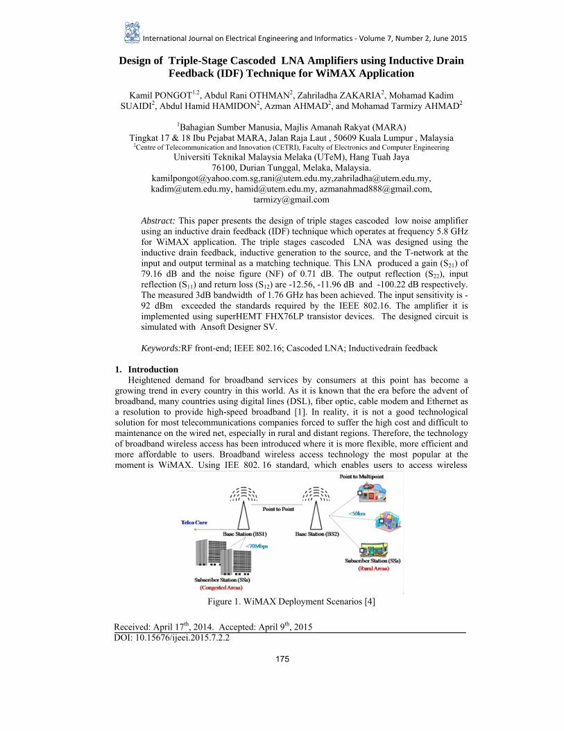
Figure 1. WiMAX Deployment Scenarios [4]
Received: April 17th, 2014. Accepted: April 9th, 2015 DOI: 10.15676/ijeei.2015.7.2.2
175
rates (70Mbps) compared to 802.11a to provide data rates only 54 Mbps up to several hundred meters, EDGE with only transfer data rates until 384 kbps to a few kilometers and CDMA2000 broadband anywhere, anytime and on any device that is installed with wireless devices [2]. WiMAX technology has more capacity (user), large area coverage (50 km) and delivers high to 2 Mbps for a few kilometersWiMAX technology has advantages in terms of high mobility performance and is one of the most user-friendly technology [3].WiMAX deployment scenarios are shown in Figure 1. The frequency spectrum of mobile WiMAX technology in NLOS applications is around 2 – 6 GHz, where the 2.3 GHz, 2.5 GHz and 3.5 GHz are dedicated for licensed spectrum while the 3.65 GHz and 5.8 GHz are dedicated for unlicensed spectrum. In this research the preferred concentration of the unlicensed spectrum at 5.8 GHz frequency. In this research the preferred concentration of the unlicensed spectrum at 5.8 GHz frequency. In the WiMAX receiver configureuration, RF front-end is designed with extensive bandwidth, low interference, high gain and sensitivity performance ensure a reliable receiving performance. The main component in the RF front-end is a low-noise amplifier (LNA). The low noise amplifier in the first stage will dominate the noise, gain, and the sensitivity performance of the RF front-end receiver. Therefore, to guarantee the implementation of the best front-back RF, LNA should be designed to optimize at the input or output impedance matching, high gain, low noise, and unconditional stability in a predetermined band. Low noise amplifier (LNA) is the core blocks in the RF front-end receiver because it will strengthen and reduce the noise figureure of the received signal from the antenna to the signal level that can be accepted by the receiver system. Selection, the correct LNA technology and timely in RF front-end receiver, is a way to get the cost-efficient and manageable. In selecting LNA technology, there are several factors that to be considered such as the selected device capabilities, the number of signal content to be integrated and the application performance requirements. Typically, most of the researchers are focusing on SiGe (BiCMOS) or CMOS transistor in designing LNAs. However, most of the commercial LNAs are designed using the GaAs-PHEMT. The use of GaAs-PHEMT devices in commercial LNAs are due to the noise figureure produced by these devices that can be reduced up to 0.5 dB. Thus, designers must find the technology that is suitable for applications to be developed to ensure a balance between the technology performances that can be obtained. However, this technology is still uncertain due to the difference in terms of architecture, specification and circuit designers themselves [5]. In this research, LNA for WiMAX applications designed using PHEMT technology and focus on the new structure. Eudyna Devices Inc FHX76LP that was found to have excellent stability at the required frequency range 5.3-6.2 GHz. This is the transistor PHEMT and provides a high gain 18 dB at 6 GHz and a low noise figureure 0.4 dB at 12 GHz. Transistor that uses low current of 10 mA with the drain-source voltage of 2 volts. Therefore, FHX76LP has been selected to design the LNA. In this research, we proposed triple stages cascaded LNA using topologies inductive drain feedback to the drain, inductive source degenerated and the T matching network at the input and output ports. This topology is designed to obtain more than 70 dB gain, and noise figureure is less than 3dB as well as maintaining in more than 1 GHz bandwidth. The proposed architecture for the configureuration RF front-end receiver a WiMAX application at 5.8 GHz as shown in Figure 2. Development of LNA in the front-end receiver is the primary focus of this research. In this configuration, it consists of triple stages cascoded LNA using the inductive drain feedback combined with source inductive degeneration, inductive RF choke placed between the two cascoded LNA amplifier and the input and output ports using the T-matching network. Adding the inductive drain feedback at the cascoded topology has provided high gain, wider bandwidth, better stability, higher reverse isolation and provide the best matching at the input or output terminal, that it also helps in increasing the bandwidth. While the addition of an inductive source generation at cascoded LNA topology enhances the bandwidth, stability and
Kamil PONGOT, et al
176
improve the input-output matching capabilities. The use of T-matching on this configuration also has helped reduce the reverse isolation and noise figure.
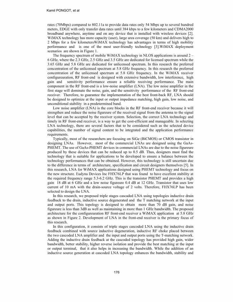
Cascoded LNA
Antena
Figure 2. RF front-end receiver architecture using a triple stagecascodedLNA configuration
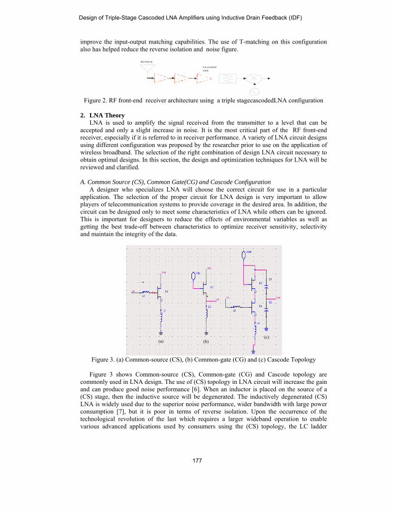
2. LNA Theory LNA is used to amplify the signal received from the transmitter to a level that can be accepted and only a slight increase in noise. It is the most critical part of the RF front-end receiver, especially if it is referred to in receiver performance. A variety of LNA circuit designs using different configuration was proposed by the researcher prior to use on the application of wireless broadband. The selection of the right combination of design LNA circuit necessary to obtain optimal designs. In this section, the design and optimization techniques for LNA will be reviewed and clarified. A. Common Source (CS), Common Gate(CG) and Cascode Configuration A designer who specializes LNA will choose the correct circuit for use in a particular application. The selection of the proper circuit for LNA design is very important to allow players of telecommunication systems to provide coverage in the desired area. In addition, the circuit can be designed only to meet some characteristics of LNA while others can be ignored. This is important for designers to reduce the effects of environmental variables as well as getting the best trade-off between characteristics to optimize receiver sensitivity, selectivity and maintain the integrity of the data.
Figure 3. (a) Common-source (CS), (b) Common-gate (CG) and (c) Cascode Topology
Figure 3 shows Common-source (CS), Common-gate (CG) and Cascode topology are commonly used in LNA design. The use of (CS) topology in LNA circuit will increase the gain and can produce good noise performance [6]. When an inductor is placed on the source of a (CS) stage, then the inductive source will be degenerated. The inductively degenerated (CS) LNA is widely used due to the superior noise performance, wider bandwidth with large power consumption [7], but it is poor in terms of reverse isolation. Upon the occurrence of the technological revolution of the last which requires a larger wideband operation to enable various advanced applications used by consumers using the (CS) topology, the LC ladder
(a) (b) (c)
Design of Triple-Stage Cascoded LNA Amplifiers using Inductive Drain Feedback (IDF)
177
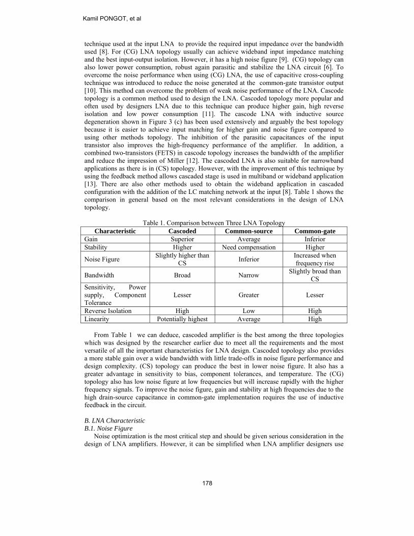
technique used at the input LNA to provide the required input impedance over the bandwidth used [8]. For (CG) LNA topology usually can achieve wideband input impedance matching and the best input-output isolation. However, it has a high noise figure [9]. (CG) topology can also lower power consumption, robust again parasitic and stabilize the LNA circuit [6]. To overcome the noise performance when using (CG) LNA, the use of capacitive cross-coupling technique was introduced to reduce the noise generated at the common-gate transistor output [10]. This method can overcome the problem of weak noise performance of the LNA. Cascode topology is a common method used to design the LNA. Cascoded topology more popular and often used by designers LNA due to this technique can produce higher gain, high reverse isolation and low power consumption [11]. The cascode LNA with inductive source degeneration shown in Figure 3 (c) has been used extensively and arguably the best topology because it is easier to achieve input matching for higher gain and noise figure compared to using other methods topology. The inhibition of the parasitic capacitances of the input transistor also improves the high-frequency performance of the amplifier. In addition, a combined two-transistors (FETS) in cascode topology increases the bandwidth of the amplifier and reduce the impression of Miller [12]. The cascoded LNA is also suitable for narrowband applications as there is in (CS) topology. However, with the improvement of this technique by using the feedback method allows cascaded stage is used in multiband or wideband application [13]. There are also other methods used to obtain the wideband application in cascaded configuration with the addition of the LC matching network at the input [8]. Table 1 shows the comparison in general based on the most relevant considerations in the design of LNA topology.
Table 1. Comparison between Three LNA Topology Characteristic Cascoded Common-source Common-gate
Gain Superior Average Inferior Stability Higher Need compensation Higher
Noise Figure Slightly higher than CS Inferior Increased when
frequency rise
Bandwidth Broad Narrow Slightly broad than CS
Sensitivity, Power supply, Component Tolerance
Lesser Greater Lesser
Reverse Isolation High Low High Linearity Potentially highest Average High From Table 1 we can deduce, cascoded amplifier is the best among the three topologies which was designed by the researcher earlier due to meet all the requirements and the most versatile of all the important characteristics for LNA design. Cascoded topology also provides a more stable gain over a wide bandwidth with little trade-offs in noise figure performance and design complexity. (CS) topology can produce the best in lower noise figure. It also has a greater advantage in sensitivity to bias, component tolerances, and temperature. The (CG) topology also has low noise figure at low frequencies but will increase rapidly with the higher frequency signals. To improve the noise figure, gain and stability at high frequencies due to the high drain-source capacitance in common-gate implementation requires the use of inductive feedback in the circuit. B. LNA Characteristic B.1. Noise Figure Noise optimization is the most critical step and should be given serious consideration in the design of LNA amplifiers. However, it can be simplified when LNA amplifier designers use
Kamil PONGOT, et al
178

the circles of the constant noise figure and constant gain circles to select usable trade-off between noise figure and gain. In general noise figure of 2-port transistor has a minimum value of the specified admittance is given by the equation (1), [14]:
2||min optYsYSGNR
FF −+= (1)
Where Ys = Gs + jBs is the source admittance presented to the transistor. Yopt = Gopt + jBopt is the optimum source admittance. RN is the equivalent noise resistance of the transistor. GS is the real part of the source admittance RN to indicate when the condition of YS ≠ Yopt happen will cause a sudden increase in noise figure. Usually at the same smith chart would plot stability circles, gain circles, noise circles, and input impedance. YS is usually chosen in between the points as a compromise between noise and gain. However, as Figure 4, Yopt and Yin can be changed and move around when there is a change in the size of transistors and add source inductance. Therefore, the inductive degeneration can be used in conjunction with transistor sizing will cause Yopt and Yin move closer together, allowing it to meet the low noise figure, high gain and excellent match input amplifier designed [15]. For low noise transistors, manufacturers usually provide Fmin, RN and Yopt by frequencies. N defined by the formula for desired noise figure, shown in equation (2):
2
0
min2
2
|1|/4||1
||opt
NS
opts
ZRFFN Γ+
−=
Γ−
Γ−Γ= (2)
Figure 4. Optimize Γs for a LNA using inductive degeneration and transistor design B.2. Stability and Power Gain Stability is one of the important characteristics in designing LNA amplifiers. Determination of stability is essential to avoid oscillation occurs at the operating frequency. The oscillation is
Yopt best for NFCascoded LNA
Yin best for gain & input match BPF
Move Yopt when changing size of transistors and
coupled inductorMixer Yin can be moved
closer to the center of smith chart
using inductive degeneration
Design of Triple-Stage Cascoded LNA Amplifiers using Inductive Drain Feedback (IDF)
179

possible if either input or output port impedance has produced a negative real part. This would imply that Γin>1 or Γout>1. This because Γin and Γout depend on the source and the load matching network. However, the stability of the amplifier depends on Γs and ΓL as presented as matching network.If low noise amplifiers is not stable, it would become useless since major properties including bandwidth, gain, noise, linearity, DC power consumption and impedance matching can be significantly degraded. For this design, there is a good stability (unconditionally stable) by employing the signal flow theory and S-parameter [15]. Alternatively, the amplifier will be unconditionally stable, when the stability factor (K) and delta factor (∆) following necessary and sufficient conditions are met:
(3)
and 121122211 <−=Δ SSSS (4)
(K > 1) and (| Δ | < 1) is condition requirement for unconditional stability. The Power Gain of 2-port networks with circuit impedance or load impedance of the power amplifier are represented with scattering coefficient classified into Available Power Gain, Power Transducer Gain and Operating Power Gain [16]. Operating power gain (GP), is the ratio between the power delivered to the load (PL) and the power input (Pin) to the network. The Operating Power Gain can be specified as an equation (5), [14] :
( )
( ) 222
2
2221
11
1
Lin
L
in
LP
S
SPPG
Γ−Γ−
Γ−=== (5)
Available power gain (GA) is the ratio between the power available from the network (Pavn)and the power available from the source (Pavs) as shown in equation (6),[14] :
222
2212
11
2
|1|1||
|1|||1
LS
S
avs
avnA S
SSP
PGΓ−Γ−
Γ−== (6)
Transducer power gain (GT) is the ratio between the power delivered to the load (PL) and the power available from the source (Pin) as shown in equation (7), [14] :
221122211
22221
|)()1)(1(|)||1)(||1(||
LSLS
LS
in
LT SSSS
SPPG
ΓΓ−Γ−Γ−Γ−Γ−
== (7)
3. Design of Tripple Stage Cascoded Using Inductive Drain Feedback (IDF) Technique
In an effort to produce a low noise amplifier with low noise figure, wide bandwidth, high gain, input and output matching circuits can reduce reflections unwanted signals and unconditional stability , we suggest the new configuration using triple stage cascoded LNA using inductive feedback to drain FET.
12
1
2112
2222
211 >
Δ+−−=
SSSS
K
Kamil PONGOT, et al
180

The proposed configuration diagram triple stage cascoded LNA is shown in Figure 5.
Figure 5. Configuration diagram Triple stage LNA cascoded LNA The targeted S-parameter specification for the triple stage LNA cascoded LNA amplifier is shown in Table 2.
Table 2. Targeted S-Parameters for a triple stage cascoded LNA amplifier S- parameter Triple stage LNA
cascoded LNA Input reflection S11 (dB) < -10 dB Return Loss S12 (dB) < -10 dB Forward Transfer S21 (dB)
>+ 70 dB
Output Reflection loss S22 (dB)
<-10 dB
Noise Figure (dB) < 3 dB Stability (K) K > 1 Bandwidth (MHz) >1000
Design configuration using a triple stage cascoded LNA and construction specifications in accordance with the specifications in Table 2. The circuit designed using PHEMT FHX76LP Transistor. S-parameters for PHEMT is shown in Table 3, where the parameters were obtained at VDD = 2V and IDS = 10mA of bias set at PHEMT.
Table 3.S-parameter from Transistor PHEMT FHX76LP datasheet Frequency GHz
S11 S12 S21 S22
5.8 GHz 0.712 0.065 8.994 0.237 Angle -86.54 33.88 178.66 -10.46
IMN Cascoded LNA
OMN IMN
Cascoded LNA
OMN VCO
DC Bias
To Terminal Source
IMN OMN Cascoded
LNA
To Terminal LoadCascoded LNA
Design of Triple-Stage Cascoded LNA Amplifiers using Inductive Drain Feedback (IDF)
181
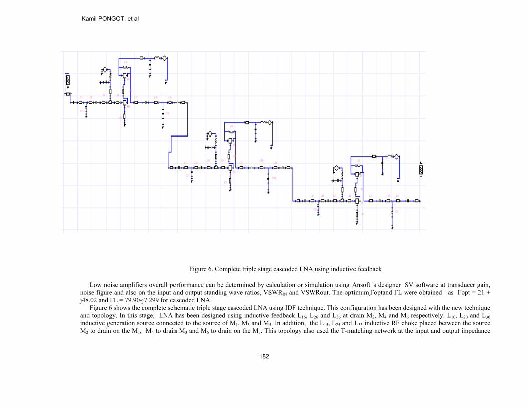
Figure 6. Complete triple stage cascoded LNA using inductive feedback
Low noise amplifiers overall performance can be determined by calculation or simulation using Ansoft 's designer SV software at transducer gain, noise figure and also on the input and output standing wave ratios, VSWRIN and VSWRout. The optimum,Γoptand ΓL were obtained as Γopt = 21 + j48.02 and ΓL = 79.90-j7.299 for cascoded LNA. Figure 6 shows the complete schematic triple stage cascoded LNA using IDF technique. This configuration has been designed with the new technique and topology. In this stage, LNA has been designed using inductive feedback L16, L26 and L36 at drain M2, M4 and M6 respectively. L10, L20 and L30 inductive generation source connected to the source of M1, M3 and M5. In addition, the L15, L25 and L35 inductive RF choke placed between the source M2 to drain on the M1, M4 to drain M3 and M6 to drain on the M5. This topology also used the T-matching network at the input and output impedance
Kamil PONGOT, et al
182
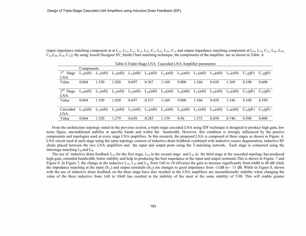
(input impedance matching component at at L11, L12, C11, L21, L22, C21 L31, L32, C31 and output impedance matching component at L18, L19, C12, L28, L29, C22,L38, L39, C32). By using Ansoft Designer SV, Smith Chart matching technique, the components of the amplifier are as shown in Table 4.
Table 4.Triple-Stage LNA Cascoded LNA Amplifier parameters Components 1st Stage LNA
L10(nH) L11(nH) L12(nH) L13(nH) L14(nH) L15(nH) L16(nH) L17(nH) L18(nH) L19(nH) C11(pF) C12(pF)
Value 0.064 1.350 1.020 0.697 0.367 1.160 9.000 1.366 0.658 1.369 0.100 0.600
2nd Stage LNA
L20(nH) L21(nH) L22(nH) L23(nH) L24(nH) L25(nH) L26(nH) L27(nH) L28(nH) L29(nH) C21(pF) C22(pF)
Value 0.064 1.350 1.020 0.697 0.337 1.160 9.000 1.366 0.658 1.346 0.100 0.550
Cascoded LNA
L30(nH) L31(nH) L32(nH) L33(nH) L34(nH) L35(nH) L36(nH) L37(nH) L38(nH) L39(nH) C31(pF) C32(pF)
Value 0.064 1.320 1.279 0.658 0.283 1.139 9.56 1.372 0.658 0.746 0.500 0.800 From the architecture topology stated in the previous section, a triple stage cascoded LNA using IDF technique is designed to produce high gain, low noise figure, unconditional stability at specific bands and widen the bandwidth. However, this condition is strongly influenced by the passive components and topologies used at every stage LNA amplifiers. In this research, the proposed LNA is composed of three stages as shown in Figure. 6. LNA circuit used at each stage using the same topology consists of inductive drain feedback combined with inductive source degeneration, inductive RF choke placed between the two LNA amplifiers and the input and output ports using the T-matching network. Each stage is connected using the interstage matching LB and CB. The use of inductive drain feedback L16 for the first stage, L26 in the second stage and L36 in the third stage at the cascoded topology has produced high-gain, extended bandwidth, better stability and help in producing the best impedance at the input and output terminals.This is shown in Figure. 7 and Figure 8. In Figure 7, the change in the inductive L16, L26 and L36 from 1nH to 10 nHvaries the gain to increase significantly from 64dB to 80 dB while the impedance matching at the input (S11) and output terminals (S22) are changes to good impedance from -11dB to - 13 dB. While in Figure 8, shown with the use of inductive drain feedback on the three stage have also resulted in the LNA amplifiers are unconditionally stability when changing the value of the three inductive from 1nH to 10nH has resulted in the stability of the meet at the same stability of 5.08. This will enable greater
Design of Triple-Stage Cascoded LNA Amplifiers using Inductive Drain Feedback (IDF)
183

changes in bandwidth from 1.37 GHz to 1.8 GHz. Adding the inductive drain feedback at the cascoded topology has provided high gain, wider bandwidth, better stability, higher reverse isolation and provide the best matching at the input or output terminal, that it also helps in increasing the bandwidth.
Figure 7. Affect changes value the L16, L26 and L36 to the overall gain and matching impedance
Figure 8. Affect changes value the L16, L26 and L36to the stability and bandwidth
Kamil PONGOT, et al
184
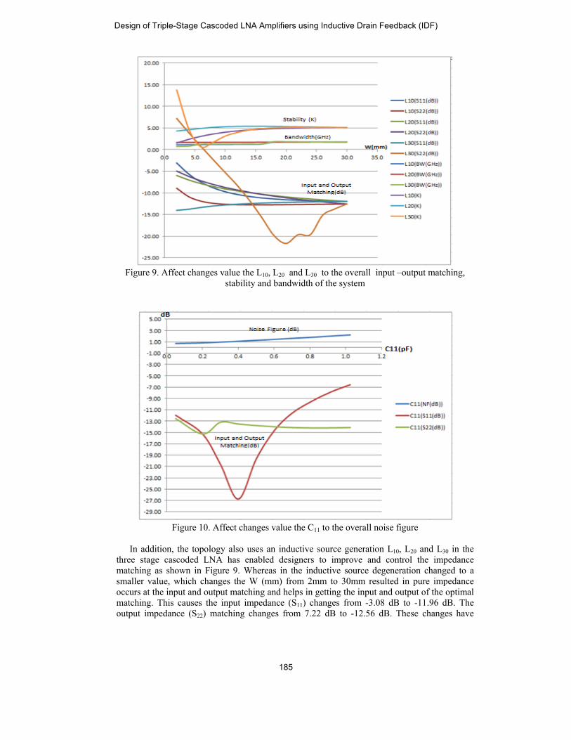
Figure 9. Affect changes value the L10, L20 and L30 to the overall input –output matching,
stability and bandwidth of the system
Figure 10. Affect changes value the C11 to the overall noise figure
In addition, the topology also uses an inductive source generation L10, L20 and L30 in the three stage cascoded LNA has enabled designers to improve and control the impedance matching as shown in Figure 9. Whereas in the inductive source degeneration changed to a smaller value, which changes the W (mm) from 2mm to 30mm resulted in pure impedance occurs at the input and output matching and helps in getting the input and output of the optimal matching. This causes the input impedance (S11) changes from -3.08 dB to -11.96 dB. The output impedance (S22) matching changes from 7.22 dB to -12.56 dB. These changes have
Design of Triple-Stage Cascoded LNA Amplifiers using Inductive Drain Feedback (IDF)
185
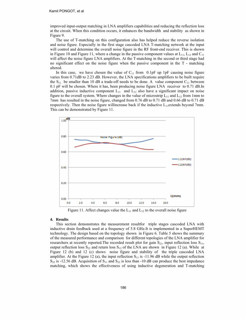
improved input-output matching in LNA amplifiers capabilities and reducing the reflection loss at the circuit. When this condition occurs, it enhances the bandwidth and stability as shown in Figure 9. The use of T-matching on this configuration also has helped reduce the reverse isolation and noise figure. Especially in the first stage cascoded LNA T-matching network at the input will control and determine the overall noise figure in the RF front-end receiver. This is shown in Figure 10 and Figure 11, where a change in the passive component values at L11, L12 and C11 will affect the noise figure LNA amplifiers. At the T-matching in the second or third stage had no significant effect on the noise figure when the passive component in the T - matching altered. In this case, we have chosen the value of C11 from 0.1pF up 1pF causing noise figure varies from 0.71dB to 2.23 dB. However, the LNA specifications amplifiers to be built require the S11 be smaller than 10 dB a trade-off needs to be done. A value component C11 between 0.1 pF will be chosen. Where it has, been producing noise figure LNA receiver to 0.71 dB.In addition, passive inductive component L11 and L12 also have a significant impact on noise figure to the overall system. Where changes in the value of microstrip L11 and L12 from 1mm to 7mm has resulted in the noise figure, changed from 0.76 dB to 0.71 dB and 0.66 dB to 0.71 dB respectively. Then the noise figure willincrease back if the inductive L11extends beyond 7mm. This can be demonstrated by Figure 11.
Figure 11. Affect changes value the L11 and L12 to the overall noise figure
4. Results This section demonstrates the measurement resultfor triple stages cascoded LNA with inductive drain feedback used at a frequency of 5.8 GHz.It is implemented in a SuperHEMT technology. The design based on the topology shown in Figure 6. Table 5 shows the summary of the measured performance and comparison for different topologies of the LNA amplifier for researchers at recently reported.The recorded result plot for gain S21, input reflection loss S11, output reflection loss S22 and return loss S12 of the LNA are shown in Figure 12 (a). While at Figure 12 (b) and 12 (c) shows noise figure and stability of the triple cascoded LNA amplifier. At the Figure 12 (a), the input reflection S11 is -11.96 dB while the output reflection S22 is -12.56 dB. Acquisition of S11 and S22 is less than -10 dB can produce the best impedance matching, which shows the effectiveness of using inductive degeneration and T-matching
Kamil PONGOT, et al
186

network at the LNA amplifier circuit. In addition, as shown in Figure 12 (a), use of cascoded topology with inductive drain feedback has resulted in transfer forward gain S21 reaches 79.16 dB at 5.8 GHz. The return loss S12 (reverse isolation) gives a very low value to -100.22 dB. The low values S12 have provided advantages in reducing LO leakage substantially which arises from capacitive paths and substrate coupling. In Figure. 12 (b) overall noise figure (NF) is 0.71 dB, which is the best result reported among the published LNAs in SuperHEMT and 0.18µm technology especially in the high frequency band.The stability K is 5.8 as shown in Figure 12 (c). . The value of stability obtained is greater than 1, and the LNA amplifiers are currently in a state of unconditionally stable.From Figure 12 (a), it is observed that, the 3dB bandwidth of around 1.76 GHz was obtained and thus complies with the targeted result of more than 1 GHz. All the result values are within the design specification, as stated in Table 2.
Table 5. Comparison performance summary of the different topology of the LNA amplifier: published and this work
Note: (-) - not stated
References Topology Technology
Input Reflection
S11 dB
Output Reflection
S22 dB
Forward
Transfer S21
dB
Return
Loss S12 dB
NF dB
BW GHz
Stability (K)
[12] Cascode Feedback
0.18-μm CMOS <-7.8 <-10 11.9 <-40 4.1-
4.6 2-6.5 -
[17]
2 stage LNA with reactive feedback
0.13-μm CMOS <-9.9 - 15.3 -34 2.5 3.1-
10.6 -
[18]
CS and CG with Parallel-to-Series Resonant Matching Network
TSMC 0.18-μm <-9 <-8 9.6-12.7 <-45 2.5-
3.9 4-9 -
[19] Cascaded LNA + RFA
SuperPHEMT -11.4 -12.4 52.4 -39.1 1.3 1.125 -
[22]
2 stage CS–CG
with source
inductive degenerati
on
0.18-μm CMOS <-12.2 - 26.25 - 2.2 0.4 20
[20]
LNA using Drain- Fully-
Differential Active
Inductive Gain-
peaking
0.18-μm CMOS <-7 <-20 17.34 -21.2 2.5 2 -
[21] LNA shunt
feedback
180nm CMOS <-11.2 <-22.8 19.9 -32.5 2.63 0.2 2.5
[This Work]
Triple cascoded
LNA using
inductive drain
feedback
SuperPHEMT -11.96 -12.56 79.16 -
100.22 0.71 1.76 5.08
Design of Triple-Stage Cascoded LNA Amplifiers using Inductive Drain Feedback (IDF)
187
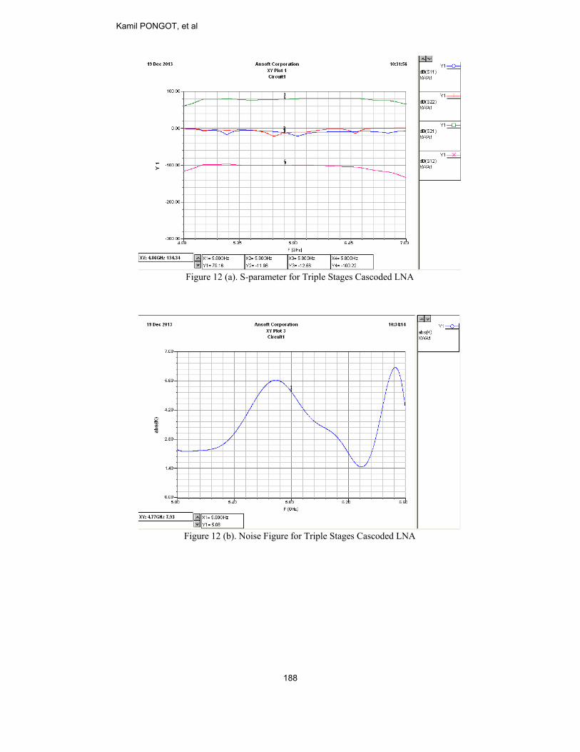
Figure 12 (a). S-parameter for Triple Stages Cascoded LNA
Figure 12 (b). Noise Figure for Triple Stages Cascoded LNA
Kamil PONGOT, et al
188
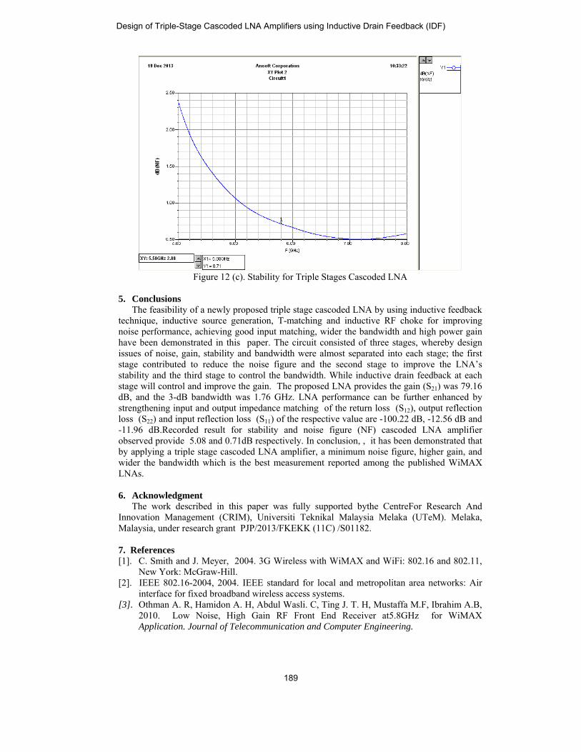
Figure 12 (c). Stability for Triple Stages Cascoded LNA
5. Conclusions The feasibility of a newly proposed triple stage cascoded LNA by using inductive feedback technique, inductive source generation, T-matching and inductive RF choke for improving noise performance, achieving good input matching, wider the bandwidth and high power gain have been demonstrated in this paper. The circuit consisted of three stages, whereby design issues of noise, gain, stability and bandwidth were almost separated into each stage; the first stage contributed to reduce the noise figure and the second stage to improve the LNA’s stability and the third stage to control the bandwidth. While inductive drain feedback at each stage will control and improve the gain. The proposed LNA provides the gain (S21) was 79.16 dB, and the 3-dB bandwidth was 1.76 GHz. LNA performance can be further enhanced by strengthening input and output impedance matching of the return loss (S12), output reflection loss (S22) and input reflection loss (S11) of the respective value are -100.22 dB, -12.56 dB and -11.96 dB.Recorded result for stability and noise figure (NF) cascoded LNA amplifier observed provide 5.08 and 0.71dB respectively. In conclusion, , it has been demonstrated that by applying a triple stage cascoded LNA amplifier, a minimum noise figure, higher gain, and wider the bandwidth which is the best measurement reported among the published WiMAX LNAs. 6. Acknowledgment The work described in this paper was fully supported bythe CentreFor Research And Innovation Management (CRIM), Universiti Teknikal Malaysia Melaka (UTeM). Melaka, Malaysia, under research grant PJP/2013/FKEKK (11C) /S01182. 7. References [1]. C. Smith and J. Meyer, 2004. 3G Wireless with WiMAX and WiFi: 802.16 and 802.11,
New York: McGraw-Hill. [2]. IEEE 802.16-2004, 2004. IEEE standard for local and metropolitan area networks: Air
interface for fixed broadband wireless access systems. [3]. Othman A. R, Hamidon A. H, Abdul Wasli. C, Ting J. T. H, Mustaffa M.F, Ibrahim A.B,
2010. Low Noise, High Gain RF Front End Receiver at5.8GHz for WiMAX Application. Journal of Telecommunication and Computer Engineering.
Design of Triple-Stage Cascoded LNA Amplifiers using Inductive Drain Feedback (IDF)
189
[4]. IEEE P802.16Rev2/D2, 2007 “DRAFT Standard for Local and metropolitan area networks, Part 16: Air Interface for Broadband Wireless Access Systems,”, pp. 2094.
[5]. A. R. Othman, A B. Ibrahim, M. N. Husain, A. H. Hamidon, and Jsam Hamidon, 2012. Low Noise Figure of Cascaded LNA at 5.8 GHz Using T-Matching Network for WiMAX Applications. International Journal of Innovation, Management and Technology, Vol. 3, No. 6.
[6]. Sudip Shekhar, Jeffery S. Walling, Sankaran Aniruddhan and David J. Allstot, 2008. CMOS VCO and LNA using tuned-input tuned-output circuits. IEEE Journal of Solid-State Circuits, vol. 43, no. 5, pp.1177-1186.
[7]. L. Belostotski and J. W. Haslett,2006. Noise figure optimization of inductively degenerated CMOS LNAs with integrated gate inductors. IEEE Trans. Circuits Syst. I: Reg. Papers, vol. 53, no. 7, pp. 1409–1422.
[8]. Tamer Ragheb, Arthur Nieuwoudt, and Yehia Massoud, 2006 . Modeling of 3.1-10.6 GHz CMOS filter-based Low noise amplifier for ultra-wideband receivers. In Proceedings of the IEEE Annual Wireless and Microwave Technology Conference (WAMICON 20'06), pp. 1-5
[9]. Chang, J.F. and Y.S. Lin, 2011. 0.99 MW 3-10 GHz Common-Gate CMOS UWB LNA using t-match input network and self-body-bias technique. Elect. Lett., 47: 658-659.
[10]. W. Zhuo, X. Li, S. Shekhar, S. H. K. Embabi, J. Pineda de Gyvez, D. J. Allstot, and E. Sánchez-Sinencio, 2005. A capacitor cross-coupled common-gate low noise amplifier. IEEE Transaction on Circuits and Systems II: Express Briefs, vol. 52, no. 12, pp. 875–879.
[11]. Hyejeong Song, Huijung Kim, Kichon Han, Jinsung Choi, Changjoon Park, and Bumman Kim, “A sub-2dB NF dual-band CMOS LNA for CDMA/WCDMA applications,” IEEE Microwave and WirelessComponents Letters, vol. 18, no. 3, pp. 212-214.2008.
[12]. Jihak Jung; Kyungho Chung; Taeyeoul Yun; Jaehoon Choi; Hoontae Kim, 2006. Ultra-wideband low noise amplifier using a cascode feedbacktopology. Silicon Monolithic Integrated Circuits in RF Systems,Digest of Papers. vol., no., pp.4.
[13]. Bevin G. Perumana1, Jing-Hong C. Zhan1, Stewart S. Taylor1, Brent R. Carlton1, and Joy Laskar, 2008. A 9.2 mW, 4-8 GHz resistive feedback CMOS LNA with 24.4 dB gain, 2 dB noise figure, and 21.5 dBm output IP3. In Proceedings of the IEEE Topical Meeting on Silicon Monolithic Integrated Circuits in RF Systems (SiRF 2008), pp. 206-209.
[14]. Abu Bakar Ibrahim, Abdul Rani Othman, Mohd Nor Husain, and Mohammad Syahrir Johal, 2011. Low Noise, High Gain LNA at 5.8GHz with Cascode and Cascaded Techniques Using T-Matching Network for Wireless Applications. International Journal of Information and Electronics Engineering, Vol. 1, No. 2.
[15]. M. Pozar, David. Microwave and RF Wireless System, 2001. Third Avenue, N. Y. John Wiley & Sons.
[16]. Leon, Michael Angelo G. Lorenzo and Maria Theresa G.De., 2010. Comparison of LNA Topology for Wimax Application in a Standard 90-nm CMOS Process. 12th International Conference on Computer Modelling and Simulation.pp-642-647.
[17]. Reiha, M.T.; Long, J.R.; Pekarik, J.J., 2006. A 1.2 V reactive-feedback 3.1-10.6 GHz ultrawideband low-noise amplifier in 0.13 /spl mu/m CMOS. Radio Frequency Integrated Circuits (RFIC) Symposium, 2006 IEEE , vol., no., pp.4 pp.,, 11-13 .
[18]. Yu-Tsung Lo; Jean-Fu Kiang, 2011. Design of Wideband LNAs Using Parallel-to-Series Resonant Matching Network Between Common-Gate andCommon-Source Stages. Microwave Theory and Techniques, IEEE Transactions on , vol.59, no.9, pp.2285,2294.
[19]. Abu Bakar Ibrahim, Abdul Rani Othman, Mohd Nor Husain, Mohammad Syahrir Johal, J. Sam Hamidon, 2012. The Cascode LNA with RFAmplifier at 5.8GHz Using T-Matching Network for WiMAX Applications. Journal of Telecommunication and Computer Engineering.
Kamil PONGOT, et al
190
[20]. ShimGainTechII, Is
[21]. KavNanRese
[22]. Gh.RampCom
for WiMA
communiin wireles
Universityprinciplesvariety ofamplifierscommuni
maAlizadehZann Flattened LNhnique. Internassue III, Septem
vyashree.P, Dr.nometer Technoearch PublicatR. Karimi, S.
plifier for 2mmunications. )
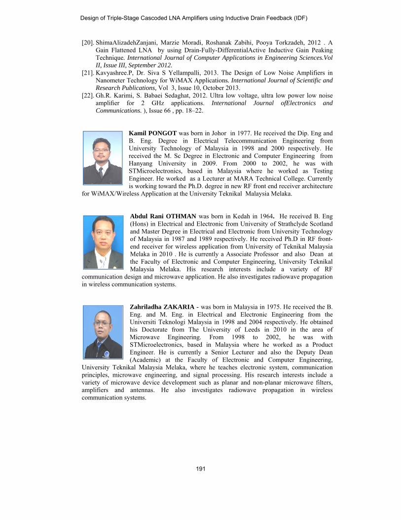
KamiB. EUnivereceivHanyaSTMiEnginis wor
AX/Wireless A
Abdu(Honsand Mof Maend rMelakthe FMalay
cation design ass communicat
ZahrEng. Univehis DMicroSTMiEngin(Acad
y Teknikal Ms, microwave f microwave ds and antencation systems
njani, Marzie NA by using ational Journamber 2012. . Siva S Yellaology for WiMtions, Vol 3, IsBabaei Sedagh
2 GHz appl), Issue 66 , pp
il PONGOT wEng. Degree ersity Technolved the M. Sc ang Universitcroelectronics,
neer. He workerking toward th
Application at t
ul Rani OTHMs) in Electrical
Master Degree alaysia in 198eceiver for wika in 2010 . H
Faculty of Elecysia Melaka. and microwaveion systems.
iladha ZAKAand M. Eng
ersiti TeknologDoctorate fromowave Enginicroelectronicsneer. He is cudemic) at the
Malaysia Melakengineering, a
device developnnas. He alss.
Moradi, RoshDrain-Fully-D
al of Computer
ampalli, 2013. MAX Applicatiossue 10, Octobhat, 2012. Ultrlications. Int
p. 18–22.
was born in Johin Electrical
logy of MalayDegree in Ele
ty in 2009. , based in Med as a Lecturhe Ph.D. degrethe University T
MAN was borl and Electroniin Electrical a7 and 1989 reireless applicatHe is currently ctronic and Co
His researce application. H
ARIA - was bog. in Electricagi Malaysia inm The Univerneering. Froms, based in Murrently a Sene Faculty of ka, where he tand signal propment such asso investigate
hanak Zabihi, PDifferentialActr Applications
The Design oons. Internatioer 2013. ra low voltageernational Jo
hor in 1977. HTelecommun
ysia in 1998 ectronic and C
From 2000 Malaysia wherer at MARA Tee in new RF frTeknikal Mala
rn in Kedah inic from Univer
and Electronic espectively. Hetion from Univa Associate P
omputer Enginch interests iHe also investi
orn in Malaysiaal and Electro
n 1998 and 200rsity of Leedm 1998 to
Malaysia wherenior Lecturer
Electronic ateaches electroocessing. His planar and no
es radiowave
Pooya Torkzadtive Inductive in Engineering
of Low Noise onal Journal of
e, ultra low poJournal ofEle
He received thenication Engiand 2000 res
Computer Engito 2002, h
ere he workeTechnical Collront end receivaysia Melaka.
n 1964. He rersity of Strathcfrom Universi
e received Ph.Dversity of TeknProfessor and neering, Univeinclude a vaigates radiowav
a in 1975. He ronic Engineer04 respectivelyds in 2010 ino 2002, hee he worked and also the
and Computeronic system, cresearch interon-planar micr
propagation
deh, 2012 . AGain Peaking
g Sciences.Vol
Amplifiers inf Scientific and
ower low noiseectronics and
e Dip. Eng andineering fromspectively. Heineering fromhe was withed as Testinglege. Currentlyver architecture
eceived B. Engclyde Scotlandity TechnologyD in RF front-nikal Malaysiaalso Dean at
ersity Teknikalariety of RFve propagation
received the Bring from they. He obtainedn the area ofe was with
as a ProductDeputy Dean
r Engineering,communicationrests include arowave filters,
in wireless
A g l
n d
e d
d m e
m h g y e
g d y -a t l
F n
. e d f h t n ,
n a , s
Design of Triple-Stage Cascoded LNA Amplifiers using Inductive Drain Feedback (IDF)
191
include a filters, amradiowave
Applicatio
MohBSc (Micro1984 TechnEngin&InteVice
variety of micmplifier, antene propagation i
AbduEng.. degrelecturEnginelectrEmbeAnalo
AzmDegrof ElectMalaBhd, worktowar
on at the Unive
MohastudeTeknElectr1998 Seber2013
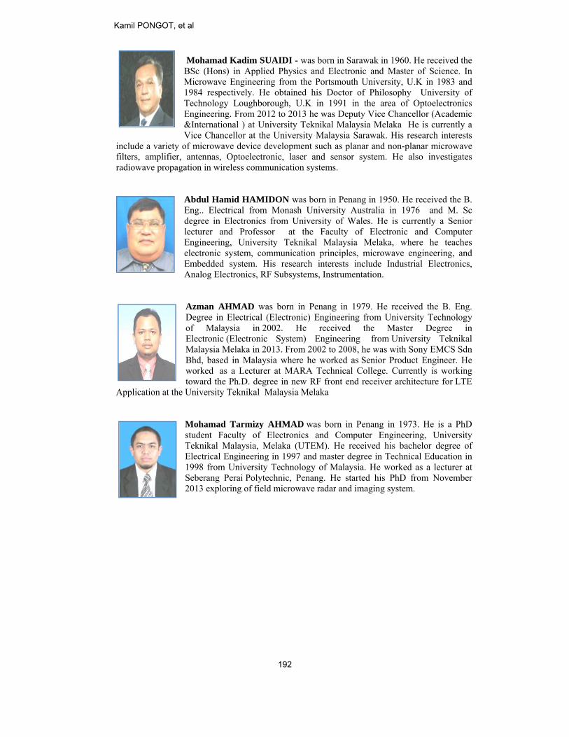
hamad Kadim (Hons) in Appowave Enginee
respectively. nology Loughbneering. From 2ernational ) at Chancellor at
crowave devicennas, Optoelecin wireless com
ul Hamid HAMElectrical fro
ee in Electronirer and Profeneering, Univeronic system, edded system. og Electronics,
an AHMADee in ElectricaMalaysia in
tronic (Electronaysia Melaka in
based in Malked as a Lecturd the Ph.D. dersity Teknikal
amad Tarmizent Faculty oikal Malaysia,rical Engineerifrom Univers
rang Perai Polexploring of fi
SUAIDI - waplied Physics ering from theHe obtained borough, U.K2012 to 2013 hUniversity Tekthe Universitye developmentctronic, laser mmunication sy
MIDON was bom Monash Uics from Univessor at theersity Teknikacommunication
His research RF Subsystem
was born in Pal (Electronic) n 2002. He nic System)n 2013. From 2laysia where hurer at MARAdegree in new Rl Malaysia Me
zy AHMAD wf Electronics , Melaka (UTEing in 1997 anity Technolog
lytechnic, Penafield microwav
as born in Sarawand Electronic
e Portsmouth Uhis Doctor of
K in 1991 in he was Deputyknikal Malaysy Malaysia Sart such as planaand sensor syystems.
born in PenangUniversity Ausersity of Walee Faculty of al Malaysia Mn principles, m
h interests incms, Instrumenta
Penang in 197Engineering f
received tEngineering
2002 to 2008, hhe worked as SA Technical CoRF front end relaka
was born in Peand Comput
EM). He recend master degry of Malaysiaang. He startee radar and im
wak in 1960. Hc and Master University, U.Kf Philosophy the area of O
y Vice Chancelia Melaka Herawak. His resar and non-planystem. He als
g in 1950. He rstralia in 1976es. He is curr
Electronic aMelaka, whermicrowave enclude Industriaation.
79. He receivefrom Universitthe Master
from Univerhe was with SoSenior Productollege. Currenreceiver archite
enang in 1973ter Engineerinived his bachee in Technica. He worked a
ed his PhD fromaging system.
He received theof Science. InK in 1983 and
University ofOptoelectronicsllor (Academice is currently asearch interestsnar microwaveso investigates
received the B6 and M. Scently a Senior
and Computerre he teachesgineering, andal Electronics,
ed the B. Eng.ty Technology
Degree inrsity Teknikalony EMCS Sdnt Engineer. He
ntly is workingecture for LTE
. He is a PhDng, Universityelor degree ofal Education inas a lecturer atom November
e n d f s c a s e s
. c r r s d ,
. y n l n e g E
D y f n t r
Kamil PONGOT, et al
192