Embed Size (px)
Citation preview

IEEE TRANSACTIONS ON ANTENNAS AND PROPAGATION, VOL. 56, NO. 7, JULY 2008 2107
Fig. 16. Variation of the simulated amplitude response versus the inductance.The dark trace corresponds to the measurement.
Fig. 17. Variation of the simulated amplitude response versus a jointly variationof the tolerance parameters. The dark trace corresponds to the measurement.
which are more sensitive and are somewhat out of this margin. It hasalso been seen that the least critical parameter is the permittivity sinceits variation affects the balun performance slightly. The most criticalparameter is the inductor while the capacitor variation shows some in-termediate performance between the one of the permittivity and the in-ductor parameters. As an example, Fig. 16 shows the amplitude balunperformance versus the independently variation of the inductance.
From the second analysis stage it can be concluded that the balunperformance suffers from larger variation than in the previous casesince all the tolerance parameters are changing at the same time. Asan example, Fig. 17 shows the amplitude balun performance versusthe jointly variation of the capacitance, inductance and permittivity.Nonetheless, the balun still presents a good amplitude and phase bal-ance performance through an approximate 4:1 bandwidth.
IV. CONCLUSION
A semi-lumped balun transformer for UHF and UWB dipoles hasbeen presented in this paper. The proposed structure is based on twoasymmetric 2nd order filters: one low pass filter and one high pass filter.The UWB performance has been achieved by shifting the HPF cutofffrequency toward lower frequencies and the LPF cutoff frequency to-ward higher ones. In addition, these filters also transform the variableantenna impedance into the desired source impedance by making useof a binomial transformer. Good agreement between simulations andmeasurements has been achieved. The prototype circuit shows goodamplitude balance with a phase difference of 180� across a 4:1 band-width from 220–820 MHz. The losses are lower than 1 dB along thewhole bandwidth.
ACKNOWLEDGMENT
The authors wish to thank Prof. A. Murphy for his help and dis-cussion during the review process and the reviewers for their helpfulcomments.
REFERENCES
[1] N. Marchand, “Transmission line conversion transformers,” Elec-tronics, vol. 17, no. 12, pp. 142–145, Dec. 1942.
[2] Y. J. Yoon, Y. Lu, R. C. Frye, M. Y. Lau, P. R. Smith, L. Ahlquist,and D. P. Kossives, “Design and characterization of multilayer spiraltransmission-line baluns,” IEEE Trans. Microw. Theory Tech., vol. 47,pp. 1841–1847, Sep. 1999.
[3] W. Bakalski, W. Simbürger, H. Knapp, H. Wohlmuth, and A. L.Scholth, “Lumped and distributed lattice-type LC-baluns,” in IEEEMTT-S Int. Microwave Symp. Digest, 2002, pp. 209–212.
[4] D. Kuylenstierna and P. Linner, “Broadband lumped element balunswith inherent impedance transformation,” IEEE Trans. Microw. TheoryTech., vol. 52, pp. 2739–2745, Dec. 2004.
[5] S. J. Parisi, “180-degree lumped-element hybrid,” in IEEE MTT-S Di-gest, 1989, pp. 1243–1246.
[6] R. E. Collin, Foundations for Microwave Engineering. New York:McGraw-Hill, 1992.
Design of Ultrawideband Mobile Phone Stubby Antenna(824 MHz-6 GHz)
Zhijun Zhang, Jean-Christophe Langer, Kevin Li, andMagdy F. Iskander
Abstract—An ultrawideband stubby antenna that covers all frequencybands between 824 MHz and 6 GHz, which include GSM 850 and 900, GPS,DVB-H US, DCS, PCS, UMTS, BT, WLAN 802.11b/g and WLAN 802.11a,with a VSWR better than 2.7:1 is described in this paper. The design pro-cedure involves obtaining a wideband resonance from 1–6 GHz and using amatching network to compensate for the high capacitance of the antenna atthe lower frequency band below 1 GHz. Parametric studies of this antennaare presented in this paper. The design was experimentally verified by con-structing an ultrawideband antenna with a volume of 5 8 30mm . Itis significant that the designed ultrawideband stubby antenna maintaineda good impedance matching and radiation efficiency at all bands. An ef-ficiency between 55 65% is achieved in the lower band including824 960 MHz band required for the GSM 850 and GSM 900 sys-tems, and an efficiency value of 67 88% is achieved at the rest of thebands starting with the GPS at 1575 MHz to 6 GHz.
Index Terms—Matching network, monopole antennas, multibandantennas, wideband antennas.
I. INTRODUCTION
With the rapid growth of mobile communication industry, moreand more functionalities are being integrated into a single mobiledevice. Meanwhile, the overall device size and also the availablespace inside a device for antennas are consistently shrinking. Five
Manuscript received July 23, 2007; revised January 2, 2008. Published July7, 2008 (projected).
Z. Zhang is with the Department of Electronic Engineering, Tsinghua Uni-versity, Beijing 100084, China.
J.-C. Langer and K. Li are with Nokia Inc., San Diego, CA 92131 USA.M. F. Iskander is with the College of Engineering, Hawaii Center for
Advanced Communications, University of Hawaii, Honolulu, HI 96822 USA(e-mail: [email protected]).
Color versions of one or more of the figures in this paper are available onlineat http://ieeexplore.ieee.org.
Digital Object Identifier 10.1109/TAP.2008.924772
0018-926X/$25.00 © 2008 IEEE
2108 IEEE TRANSACTIONS ON ANTENNAS AND PROPAGATION, VOL. 56, NO. 7, JULY 2008
years ago, a cell phone needed only to cover four bands. In thenear future, a state of art cell phone could have antennas thatcover nine bands including Global System for Mobile (GSM) 850(824–894 MHz), GSM 900 (880–960 MHz), Global PositioningSystem – GPS (1575 MHz), Digital Video Broadcasting-HandheldUS (DVB-H US) (1670–1675 MHz), Digital Communication System(DCS) (1710–1880 MHz), Personal Communication System (PCS)(1850–1990) MHz, Universal Mobile Telecommunications System(UMTS) or 3G (1920–2175 MHz), Bluetooth or Wireless Local AreaNetwork (WLAN) 802.11b/g (2400–2484 MHz) and WLAN 802.11a(5150–5875 MHz). More recently cell phone diversity antennas areemerging and this requires another set of antennas that cover up toseven bands: GSM850, GSM900, DCS, PCS, UMTS, WLAN 802.11gand 802.11a multiple-input multiple-output (MIMO) system.
Since the early 1990s, the cell phone industry started adopting multi-band cell phone antennas, such as multi-pitch helix antennas, mono-helix antennas, meander line antennas and multi-band planar inverted-Fantennas (PIFA) [1]. Those kinds of antennas can be used to cover up tothree or even four bands (GSM 850 and 900, DCS and PCS). With thehelp of a parasitic element [2], active switch and/or dual port antennamodule, PIFA type antennas has been used to support up to six bands(GSM 850 and 900, GPS, DCS, PCS and UMTS). Guo et al. [3] havereported a double layer PIFA antenna with parasitic plate that can coversix bands (GSM 900, GPS, DCS, PCS, UMTS and 802.11b/g) with avolume of 36 � 17 � 8 mm3. Li et al. [4] reported a nine-band internalantenna, which was used to cover the same bands as the stubby antennadescribed in this paper, by using a large size radiating element. Li’santenna was installed perpendicular to the circuit board with an areaof 50 mm � 50 mm. Wong et al. [5] reported a cylindrical monopoleantenna that covers from 1.8 GHz to 10.6 GHz with a volume of 20�10�10 mm
3. Liu [6] reported a stamping antenna that covers from 1.713to 12.68 GHz with a volume of 20 � 10 � 10 mm3. Liu’s antenna canbe easily fabricated by folding a single metal plate, with no additionalwelding process required. The antenna proposed in this paper uses asimilar manufacture process.
To improve the antenna matching, matching networks have beenwidely used in cell phone antenna designs [8], [9] since 1990s. Tzortza-kakis et al. [8] used a two-component high pass matching network toimprove the lower band matching. Ollikainen et al. [9] used an open-ended quarter wavelength transmission line at lower frequency to forma secondary resonance thus improve the matching at the lower band.This paper used a four-component matching network to match boththe lower and higher band simultaneously.
In this paper we present an ultrawideband stubby antenna that coversall current cell phone communication bands from 824 MHz to 6 GHz.This paper is based on [10]. The antenna has a volume of 5�8�30mm3.The antenna is made of a folded V shape stamped sheet metal, whichcan be easily manufactured, and folded to form a three-dimensionalshape. An efficiency value between 55 � 65% is achieved at the lowerband that includes the 824 � 960 MHz range, and an efficiency of67 � 88% is achieved at the upper desirable band from 1575 MHz to6 GHz.
II. DESIGN APPROACH AND SIMULATION RESULTS
It is well known that tapered structures can exhibit wide band prop-erties. Bi-conical, disc-conical and bow-tie antennas [5], [7] can easilyachieve ultrawideband coverage. For these kinds of antennas, however,the total length of antenna determines the lowest working frequencyand the precision of the tapered feature near the feeding point deter-mines the highest operating frequency.
For a discone antenna with a lowest working frequency of 800 MHz,the length and the diameter of the antenna are all about 160 mm. Thesize of this antenna is, therefore, too large to be integrated into modern
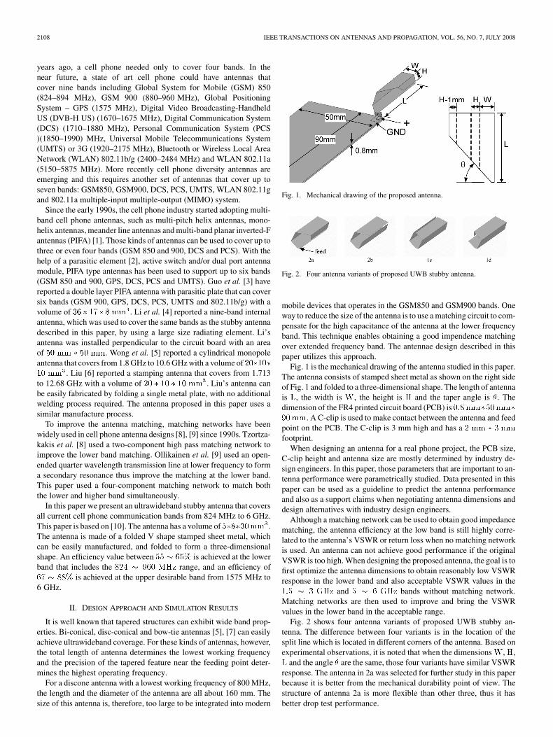
Fig. 1. Mechanical drawing of the proposed antenna.
Fig. 2. Four antenna variants of proposed UWB stubby antenna.
mobile devices that operates in the GSM850 and GSM900 bands. Oneway to reduce the size of the antenna is to use a matching circuit to com-pensate for the high capacitance of the antenna at the lower frequencyband. This technique enables obtaining a good impendence matchingover extended frequency band. The antennae design described in thispaper utilizes this approach.
Fig. 1 is the mechanical drawing of the antenna studied in this paper.The antenna consists of stamped sheet metal as shown on the right sideof Fig. 1 and folded to a three-dimensional shape. The length of antennais L, the width is W, the height is H and the taper angle is �. Thedimension of the FR4 printed circuit board (PCB) is 0:8mm�50mm�90mm. A C-clip is used to make contact between the antenna and feedpoint on the PCB. The C-clip is 3 mm high and has a 2 mm � 3 mm
footprint.When designing an antenna for a real phone project, the PCB size,
C-clip height and antenna size are mostly determined by industry de-sign engineers. In this paper, those parameters that are important to an-tenna performance were parametrically studied. Data presented in thispaper can be used as a guideline to predict the antenna performanceand also as a support claims when negotiating antenna dimensions anddesign alternatives with industry design engineers.
Although a matching network can be used to obtain good impedancematching, the antenna efficiency at the low band is still highly corre-lated to the antenna’s VSWR or return loss when no matching networkis used. An antenna can not achieve good performance if the originalVSWR is too high. When designing the proposed antenna, the goal is tofirst optimize the antenna dimensions to obtain reasonably low VSWRresponse in the lower band and also acceptable VSWR values in the1:5 � 3 GHz and 5 � 6 GHz bands without matching network.Matching networks are then used to improve and bring the VSWRvalues in the lower band in the acceptable range.
Fig. 2 shows four antenna variants of proposed UWB stubby an-tenna. The difference between four variants is in the location of thesplit line which is located in different corners of the antenna. Based onexperimental observations, it is noted that when the dimensions W,H,L and the angle � are the same, those four variants have similar VSWRresponse. The antenna in 2a was selected for further study in this paperbecause it is better from the mechanical durability point of view. Thestructure of antenna 2a is more flexible than other three, thus it hasbetter drop test performance.
IEEE TRANSACTIONS ON ANTENNAS AND PROPAGATION, VOL. 56, NO. 7, JULY 2008 2109
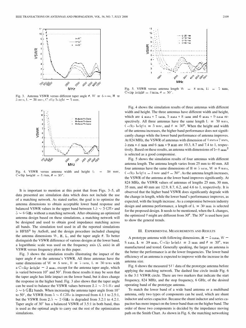
Fig. 3. Antenna VSWR versus different taper angle �. W = 8 mm, H =5 mm, L = 30 mm, C-clip height = 3 mm.
Fig. 4. VSWR versus antenna width and height L = 30 mm,C-clip height = 3 mm, � = 30 .
It is important to mention at this point that from Figs. 3–5, alldata presented are simulation data which does not include the useof a matching network. As stated earlier, the goal is to optimize theantenna dimensions to obtain acceptable lower band response andbalanced VSWR values in the upper band between 1:5 � 3 GHz and5 � 6 GHz without a matching network. After obtaining an optimizedantenna design based on these simulations, a matching network willbe designed and used to obtain good impedance matching acrossall bands. The simulation tool used in all the reported simulationsis HFSS® by AnSoft, and the design procedure included changingthe antenna dimensions W, H, L, and the taper angle �. To betterdistinguish the VSWR difference of various designs at the lower band,a logarithmic scale was used on the frequency axis (X axis) in allVSWR versus frequency plots in this paper.
Fig. 3 shows the simulation results illustrating the impact of thetaper angle � on the antenna’s VSWR. All three antennas have thesame dimensions of W = 8 mm, H = 5 mm, L = 30 mm witha C-clip height = 3 mm, except for the antenna taper angle, whichis varied between 10� and 50�. From these results it may be seen thatthe taper angle has little impact on the lower band, but it does changethe response in the higher band. Fig. 3 also shows that the taper anglecan be used to balance the VSWR values between 2:5 � 3 GHz and5 � 6 GHz bands. When increasing the antenna taper angle from 10�
to 50�, the VSWR from 5 � 6 GHz is improved from 4.1:1 to 2.5:1,but the VSWR from 2:5 � 3 GHz is degraded from 3.2:1 to 4.2:1.Taper angle of 30� has a balanced VSWR of 3.5:1 in both band, thusis used as the optimal angle to carry out the rest of the optimizationsimulations.
Fig. 5. VSWR versus antenna length W = 8 mm, H = 5 mm,C-clip height = 3 mm, � = 30 .
Fig. 4 shows the simulation results of three antennas with differentwidth and height. The three antennas have different width and height,which are 4 mm � 7 mm, 5 mm � 8 mm and 6 mm � 9 mm re-spectively. All three antennas have the same length L = 30 mm,C-clip height = 3 mm, and � = 30�. When the height and widthof the antenna increases, the higher band performance does not signifi-cantly change while the lower band performance of antenna improves.At 824 MHz, the VSWR of antennas with dimension of 4mm�7mm,5 mm � 8 mm and 6 mm � 9 mm are 10.3, 8.7 and 7.4 to 1, respec-tively. Based on these results, an antenna with dimensions of 5�8mm2
is selected as a good compromise.Fig. 5 shows the simulation results of four antennas with different
antenna length. The antenna length varies from 25 mm to 40 mm. Allfour antennas have the same dimensions of H = 5 mm, W = 8 mm,C-clip height = 3mm and � = 30�. As the antenna length increases,the VSWR of the antenna at the lower band improves significantly. At824 MHz, the VSWR values of antennas of lengths 25 mm, 30 mm,35 mm, and 40 mm are 12.9, 8.7, 6.2, and 4.6 to 1, respectively. It isobserved that the higher band VSWR does significantly degrade withthe change in length, while the lower band’s performance improves, asexpected, with the length increase. As a compromise between industrydesign and antenna performance, a length of L = 30 mm is selectedfor the proposed design. It needs to be mentioned, when the L changes,the optimized � might are different from 30�. The 30� is used here justto show the general trends.
III. EXPERIMENTAL MEASUREMENTS AND RESULTS
A prototype antenna with following dimensions, H = 5 mm, W =
8 mm, L = 30 mm, C-clip height = 3 mm and � = 30�, wasmanufactured and tested. Generally speaking, the larger an antenna isthe better the performance is at the lower frequencies. The lower bandefficiency of an antenna is expected to improve with the increase in theantenna size.
Fig. 6 shows the measured S11 data of the prototype antenna beforeapplying the matching network. The dashed line circle inside Fig. 6is the 3:1 VSWR circle. There are two markers that indicate the startfrequency, 824 MHz, and the stop frequency, 6 GHz, of the desiredoperating band of the prototype antenna.
To match the lower band of a wide band antenna or a multibandantenna, only two types of components can be used, which are shuntinductor and series capacitor. Because the shunt inductor and series ca-pacitor has more impact on the lower band than on the higher band. Theorder of those two components is decided by the impedance movingpath on the Smith Chart. As shown in Fig. 6, the matching networking
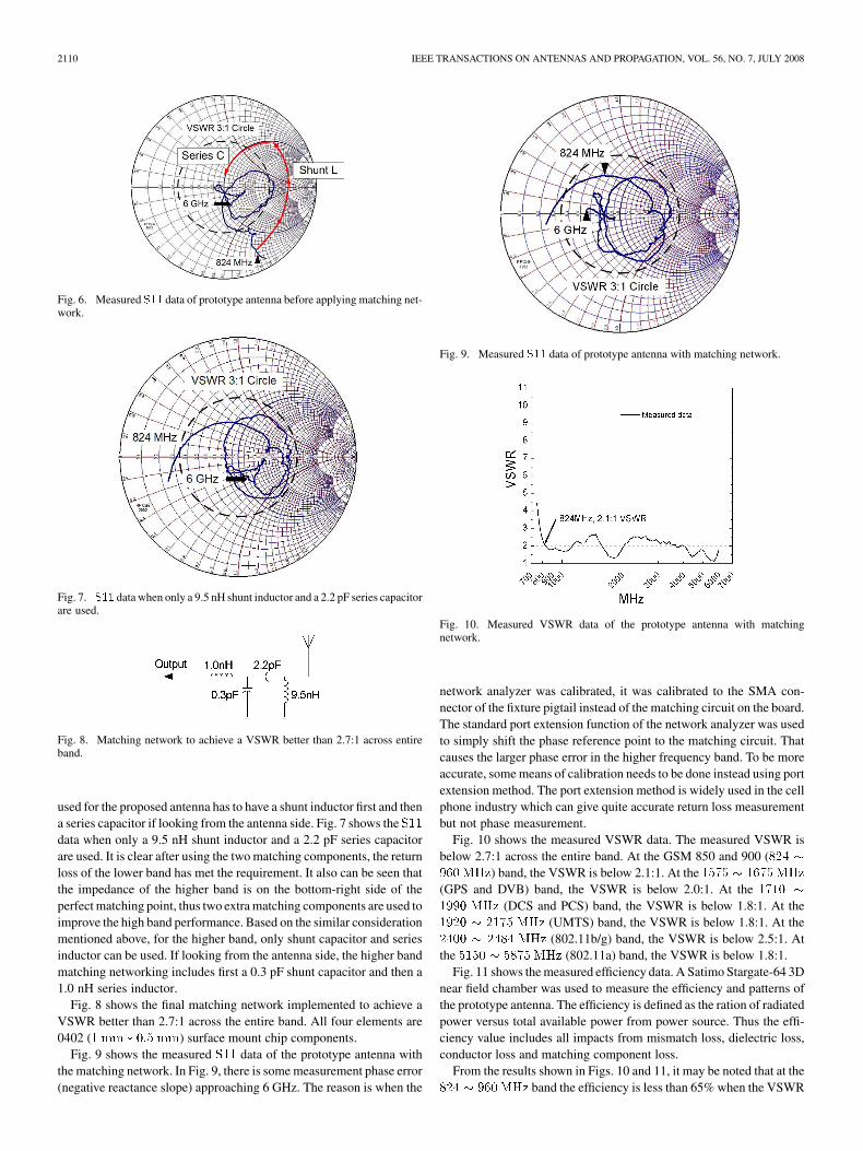
2110 IEEE TRANSACTIONS ON ANTENNAS AND PROPAGATION, VOL. 56, NO. 7, JULY 2008
Fig. 6. Measured S11 data of prototype antenna before applying matching net-work.
Fig. 7. S11 data when only a 9.5 nH shunt inductor and a 2.2 pF series capacitorare used.
Fig. 8. Matching network to achieve a VSWR better than 2.7:1 across entireband.
used for the proposed antenna has to have a shunt inductor first and thena series capacitor if looking from the antenna side. Fig. 7 shows the S11data when only a 9.5 nH shunt inductor and a 2.2 pF series capacitorare used. It is clear after using the two matching components, the returnloss of the lower band has met the requirement. It also can be seen thatthe impedance of the higher band is on the bottom-right side of theperfect matching point, thus two extra matching components are used toimprove the high band performance. Based on the similar considerationmentioned above, for the higher band, only shunt capacitor and seriesinductor can be used. If looking from the antenna side, the higher bandmatching networking includes first a 0.3 pF shunt capacitor and then a1.0 nH series inductor.
Fig. 8 shows the final matching network implemented to achieve aVSWR better than 2.7:1 across the entire band. All four elements are0402 (1 mm � 0:5 mm) surface mount chip components.
Fig. 9 shows the measured S11 data of the prototype antenna withthe matching network. In Fig. 9, there is some measurement phase error(negative reactance slope) approaching 6 GHz. The reason is when the
Fig. 9. Measured S11 data of prototype antenna with matching network.
Fig. 10. Measured VSWR data of the prototype antenna with matchingnetwork.
network analyzer was calibrated, it was calibrated to the SMA con-nector of the fixture pigtail instead of the matching circuit on the board.The standard port extension function of the network analyzer was usedto simply shift the phase reference point to the matching circuit. Thatcauses the larger phase error in the higher frequency band. To be moreaccurate, some means of calibration needs to be done instead using portextension method. The port extension method is widely used in the cellphone industry which can give quite accurate return loss measurementbut not phase measurement.
Fig. 10 shows the measured VSWR data. The measured VSWR isbelow 2.7:1 across the entire band. At the GSM 850 and 900 (824 �960MHz) band, the VSWR is below 2.1:1. At the 1575 � 1675MHz
(GPS and DVB) band, the VSWR is below 2.0:1. At the 1710 �
1990 MHz (DCS and PCS) band, the VSWR is below 1.8:1. At the1920 � 2175 MHz (UMTS) band, the VSWR is below 1.8:1. At the2400 � 2484 MHz (802.11b/g) band, the VSWR is below 2.5:1. Atthe 5150 � 5875 MHz (802.11a) band, the VSWR is below 1.8:1.
Fig. 11 shows the measured efficiency data. A Satimo Stargate-64 3Dnear field chamber was used to measure the efficiency and patterns ofthe prototype antenna. The efficiency is defined as the ration of radiatedpower versus total available power from power source. Thus the effi-ciency value includes all impacts from mismatch loss, dielectric loss,conductor loss and matching component loss.
From the results shown in Figs. 10 and 11, it may be noted that at the824 � 960MHz band the efficiency is less than 65% when the VSWR
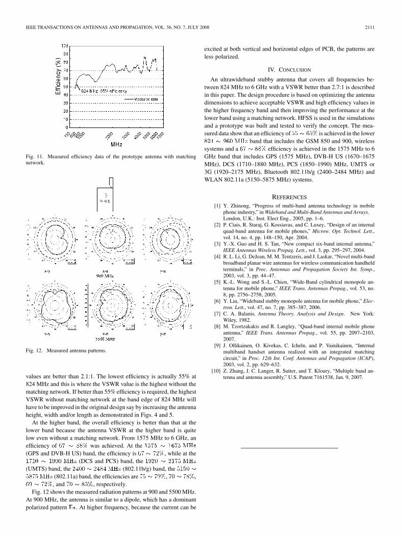
IEEE TRANSACTIONS ON ANTENNAS AND PROPAGATION, VOL. 56, NO. 7, JULY 2008 2111
Fig. 11. Measured efficiency data of the prototype antenna with matchingnetwork.
Fig. 12. Measured antenna patterns.
values are better than 2.1:1. The lowest efficiency is actually 55% at824 MHz and this is where the VSWR value is the highest without thematching network. If better than 55% efficiency is required, the highestVSWR without matching network at the band edge of 824 MHz willhave to be improved in the original design say by increasing the antennaheight, width and/or length as demonstrated in Figs. 4 and 5.
At the higher band, the overall efficiency is better than that at thelower band because the antenna VSWR at the higher band is quitelow even without a matching network. From 1575 MHz to 6 GHz, anefficiency of 67 � 88% was achieved. At the 1575 � 1675 MHz
(GPS and DVB-H US) band, the efficiency is 67 � 72%, while at the1710 � 1990 MHz (DCS and PCS) band, the 1920 � 2175 MHz
(UMTS) band, the 2400 � 2484 MHz (802.11b/g) band, the 5150 �5875MHz (802.11a) band, the efficiencies are 75 � 79%, 70 � 78%,69 � 72%, and 70 � 83%, respectively.
Fig. 12 shows the measured radiation patterns at 900 and 5500 MHz.At 900 MHz, the antenna is similar to a dipole, which has a dominantpolarized pattern E� . At higher frequency, because the current can be
excited at both vertical and horizontal edges of PCB, the patterns areless polarized.
IV. CONCLUSION
An ultrawideband stubby antenna that covers all frequencies be-tween 824 MHz to 6 GHz with a VSWR better than 2.7:1 is describedin this paper. The design procedure is based on optimizing the antennadimensions to achieve acceptable VSWR and high efficiency values inthe higher frequency band and then improving the performance at thelower band using a matching network. HFSS is used in the simulationsand a prototype was built and tested to verify the concept. The mea-sured data show that an efficiency of 55 � 65% is achieved in the lower824 � 960 MHz band that includes the GSM 850 and 900, wirelesssystems and a 67 � 88% efficiency is achieved in the 1575 MHz to 6GHz band that includes GPS (1575 MHz), DVB-H US (1670–1675MHz), DCS (1710–1880 MHz), PCS (1850–1990) MHz, UMTS or3G (1920–2175 MHz), Bluetooth 802.11b/g (2400–2484 MHz) andWLAN 802.11a (5150–5875 MHz) systems.
REFERENCES
[1] Y. Zhinong, “Progress of multi-band antenna technology in mobilephone industry,” in Wideband and Multi-Band Antennas and Arrays.London, U.K.: Inst. Elect Eng., 2005, pp. 1–6.
[2] P. Ciais, R. Staraj, G. Kossiavas, and C. Luxey, “Design of an internalquad-band antenna for mobile phones,” Microw. Opt. Technol. Lett.,vol. 14, no. 4, pp. 148–150, Apr. 2004.
[3] Y.-X. Guo and H. S. Tan, “New compact six-band internal antenna,”IEEE Antennas Wireless Propag. Lett., vol. 3, pp. 295–297, 2004.
[4] R. L. Li, G. DeJean, M. M. Tentzeris, and J. Laskar, “Novel multi-bandbroadband planar wire antennas for wireless communication handheldterminals,” in Proc. Antennas and Propagation Society Int. Symp.,2003, vol. 3, pp. 44–47.
[5] K.-L. Wong and S.-L. Chien, “Wide-Band cylindrical monopole an-tenna for mobile phone,” IEEE Trans. Antennas Propag., vol. 53, no.8, pp. 2756–2758, 2005.
[6] Y. Liu, “Wideband stubby monopole antenna for mobile phone,” Elec-tron. Lett., vol. 47, no. 7, pp. 385–387, 2006.
[7] C. A. Balanis, Antenna Theory. Analysis and Design. New York:Wiley, 1982.
[8] M. Tzortzakakis and R. Langley, “Quad-band internal mobile phoneantenna,” IEEE Trans. Antennas Propag., vol. 55, pp. 2097–2103,2007.
[9] J. Ollikainen, O. Kivekas, C. Icheln, and P. Vainikainen, “Internalmultiband handset antenna realized with an integrated matchingcircuit,” in Proc. 12th Int. Conf. Antennas and Propagation (ICAP),2003, vol. 2, pp. 629–632.
[10] Z. Zhang, J. C. Langer, R. Sutter, and T. Kfoury, “Multiple band an-tenna and antenna assembly,” U.S. Patent 7161538, Jan. 9, 2007.
![Horizontally Polarized Omnidirectional Antenna Array …oa.ee.tsinghua.edu.cn/~zjzhang/papers_pdf/ap_2016_3.pdf · [19] L. I. Schiff, Quantum Mechanics. London, U.K.: McGraw-Hill,](https://img.pdfslide.net/doc/110x75/5b68a29e7f8b9af23e8ce89a/horizontally-polarized-omnidirectional-antenna-array-oaee-zjzhangpaperspdfap20163pdf.jpg)