Embed Size (px)
Citation preview

95
Itakura et al.: Design of Via Structure for High-speed Signal Transmission (1/8)
1. IntroductionBy the improvement of the recent rapid high frequency
technology, the signal data rate 28 Gbps (CEI 3.0) has
been put to practical use implemented by the multilayer
printed circuit board and 56 Gbps is planned in the next
generation. Therefore, the higher harmonic waves are
already beyond 50 GHz, and designing concepts for the
high-speed signal integrity should become more important
and be updated in order to ensure data reliability.
When a multilayer circuit board is used to increase the
signal density, via structures are unavoidable to connect
signal paths and planes. However, it has been known that
the high-speed via transmission causes impedance discon-
tinuities which cannot be ignored. And it is clear these dis-
continuities could lead to various signal integrity prob-
lems.[1–5] For example, the high-speed via transmission
could induce increases of the reflection, cross-talk, jitter,
and insertion loss as a result. In the previous studies, it
was proven that the above discontinuities are caused by
the electromagnetic couplings between the signal via and
the solid ground layers. And those couplings were
expressed in the equivalent circuit as the parasitic capaci-
tances between a signal via and solid ground layers,[6–14]
as shown Fig. 1. In this case, the design concepts of
decrease in the above capacitances, such as adjustments of
the via and through-hole structures, could be effective to
improve the high-speed via transmission characteris-
tics.[15–17] However, It has been known recently that the
via transmission give rise to not only the problems of
impedance discontinuities, but also the undesirable signal
power emission or leak into the interval of the solid ground
planes which have the parallel plate transmission mode.
The above emission has also been known to end up to
cause EMI problems against the external electric equip-
ment.[18–21]
The circuit board manufacturer attempts to reduce costs
of multilayer circuit board under compulsion, according to
the significant progress of the signal data rate in recent
years. For instance, there are two ways to reduce it. One is
the adoption of the single-ended transmitter line. The
[Technical Paper]
Design of Via Structure for High-speed Signal Transmission in
Multilayer Circuit BoardHiroshi Itakura, Keitaro Yamagishi, and Yoshihiro Akeboshi
*Information Technology R&D Center, Mitsubishi Electric Corporation, 5-1-1 Ofuna, Kamakura city, 247-8501, Japan
(Received August 17, 2015; accepted November 16, 2015)
Abstract
Via structures are unavoidable to connect signal paths when a multilayer circuit board is used to increase the signal
density. It however becomes clear recently that high-speed via transmission causes not only impedance discontinuities
but also the undesirable leak of signal power as the emission with the parallel plate transmission mode between the solid
ground planes. In order to solve above problems, the suppression method for them is proposed in this paper. The pro-
posed method is expanding a part of the clearance around the signal via as a fan shape. As a result of the 3D electromag-
netic simulation, we confirmed that it could improve the levels of the signal power emissions from signal via from 57% to
30%. This method might be available to low-cost production of the multilayer circuit board in the next generation, in the
point that it is applicable to conventional low-cost substrate manufacturing methods.
Keywords: Via, Signal Integrity, Parallel Plate, Printed Circuit Board (PCB), Emission Loss, Parasitic Capacitance
Copyright © The Japan Institute of Electronics Packaging
Fig. 1 Signal power emission dielectric between ground lay-ers.

96
Transactions of The Japan Institute of Electronics Packaging Vol. 8, No. 1, 2015
other way is the reduction of layers of multilayer circuit
board. Here, only inner layers should be removed, as
shown in Fig. 1. This is because the standard thickness for
the board should be maintained. In the view of the cross-
talk in addition, adjacent layers must be separated with
each other.
While the distance between the adjacent ground planes
must become longer in the above situation, it has been
known that the unwanted signal power emissions might be
occurred at the signal via into the dielectric between
ground planes when the high-speed signal goes through it.
It is clear and obvious that the involved emission causes
remarkable noises and degradations of transmission char-
acteristics at high frequencies in the multilayer circuit
board. However, the previous studies do not mentioned
obviously the electromagnetic behaviors of the signal
power emissions at higher frequency band and why this
phenomenon is occurred, at 30~50 GHz. As a result, there
is no suppression method for that undesirable signal
power emission. It could be considered that surrounding
the signal via with a sufficient number of ground vias, as
the electromagnetic shield, of course could suppress the
above phenomenon. Nevertheless, this method must take
more regions for high density wiring and costs of multi-
layer circuit board.
In this paper, we therefore proposed the simple suppres-
sion method for the undesirable power emissions from the
via transmission into the dielectric between ground planes.
Specifically, only to the direction that wanted to suppress
the unnecessary signal power emission, the clearance
around the via is extended simply into a fan shape. At first,
we considered the causes of the undesirable signal power
emission at high frequency from the signal via into dielec-
tric between ground planes in chapter II. These are
described by evaluating electromagnetic fields simulated
by use of 3D analysis models of the single-ended via trans-
mission implemented by the conventional 4 layer printed
circuit board as the basic study.[22] Based on the chapter
II, the availabilities of the proposed unique clearance
structure around the high-speed via are evaluated in chap-
ter III. As a consequence, by using this proposed method
in this paper, the low-cost production of the multilayer cir-
cuit board in the next generation is available, in the point
that it is applicable to conventional low-cost substrate man-
ufacturing methods.
2. Signal Power Emission Problems from High-speed Via Transmission
Influences and causes of the undesirable signal power
emission into the dielectric between ground planes from
the signal via in multilayer circuit board were evaluated in
the preceding study.[22] In order to consider them, the E
field intensity distributions around it were simulated by
use of HFSS (Ansys) in this chapter. The 3D analysis
model of the single-ended via transmission implemented
by the conventional 4 layer circuit board is used in this
investigation.
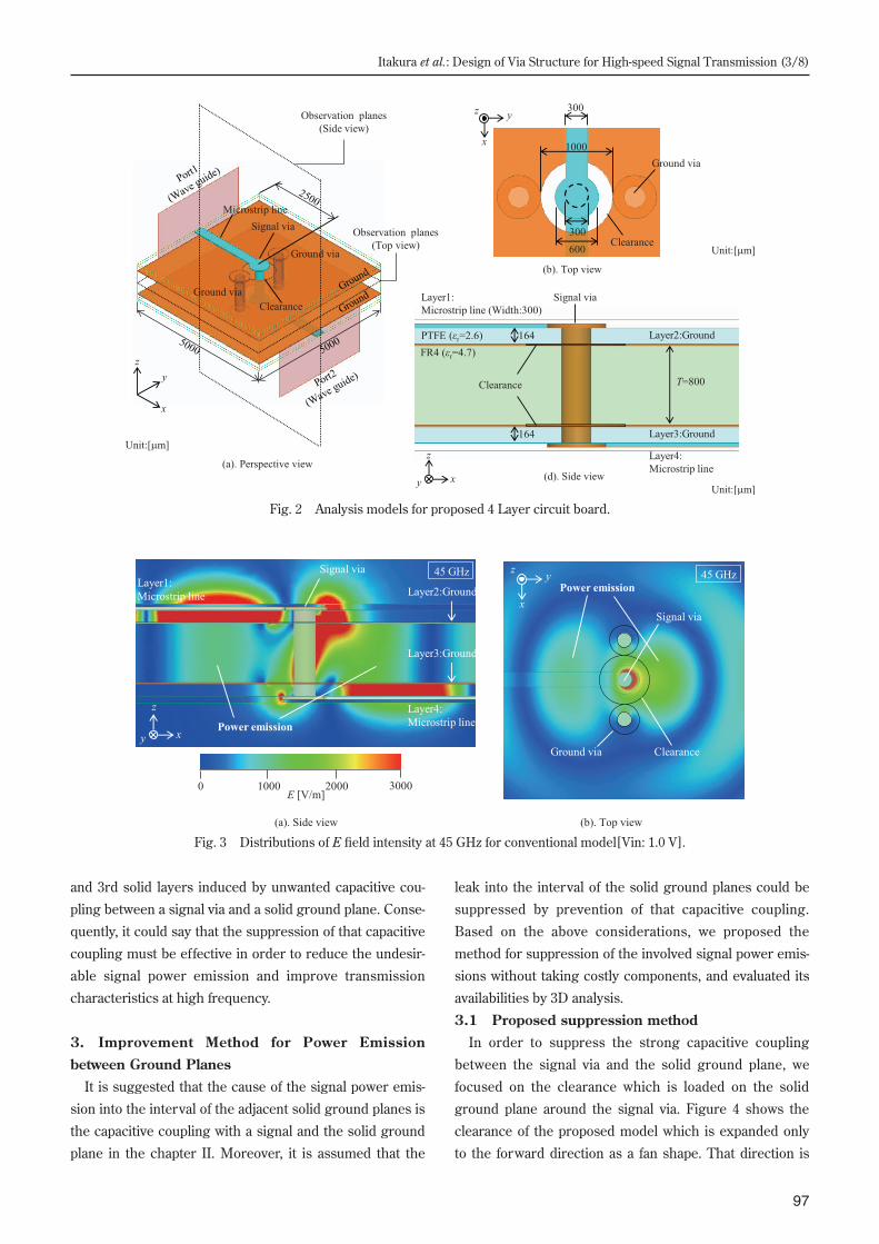
The E field intensity distributions at a moment of the
specific phase are analyzed at 45 GHz for the conventional
model, as shown in Fig. 2. The 3D analysis model of the
conventional 4 layer circuit board we evaluated is as the
layer 1 and layer 4 are the signal layers, two microstrip
lines are loaded on there respectively, and connected by a
signal via. Then, waveguide port 1 and 2 are placed at
edges of microstrip lines on their own layers. The solid
ground planes are set to the layer 2 and layer 3 of the
model. They are connected by the two ground vias which
are located on both side of the signal via for the isolation
from another transmission system. The input voltage to
the microstrip line at the 1st layer is 1.0 V.
The diameters of the barrel and the pad of the vias are
set to be 300 μm and 600 μm, respectively as typical param-
eters. The characteristic impedance of this transmission
system is 50 Ω. The diameter of the clearance around a
signal via is set to be 1,000 μm. The solid ground distance
between the layer 2 and the layer 3 mentioned as T is 800
μm as generally adopted with a 4 layer circuit board.
As the results of the side view the E field intensity distri-
bution as shown in Fig. 3 (a), it is confirmed that the
strong E field is induced between the 2nd and 3rd solid
ground planes. The electric potential difference must be
occurred between the two solid ground planes because of
the distance between them is approximately 1/4 wave-
length at 45 GHz. Then, this induced E field might propa-
gate between the ground layers in ±x direction as the
undesirable signal power emission. On the other hand,
shown in, the top view of which the observation plane is at
the intermediate point between the 2nd/3rd ground layers
in Fig. 3 (b), it shows that the induced E fields are radiated
in all directions from the signal via concentrically, except
the direction to the ground vias.
From the results of the E field intensity distributions, we
assumed that the signal power emissions at 40~50 GHz are
caused by the electric potential difference between the 2nd
97
Itakura et al.: Design of Via Structure for High-speed Signal Transmission (3/8)
and 3rd solid layers induced by unwanted capacitive cou-
pling between a signal via and a solid ground plane. Conse-
quently, it could say that the suppression of that capacitive
coupling must be effective in order to reduce the undesir-
able signal power emission and improve transmission
characteristics at high frequency.
3. Improvement Method for Power Emission between Ground Planes
It is suggested that the cause of the signal power emis-
sion into the interval of the adjacent solid ground planes is
the capacitive coupling with a signal and the solid ground
plane in the chapter II. Moreover, it is assumed that the
leak into the interval of the solid ground planes could be
suppressed by prevention of that capacitive coupling.
Based on the above considerations, we proposed the
method for suppression of the involved signal power emis-
sions without taking costly components, and evaluated its
availabilities by 3D analysis.
3.1 Proposed suppression methodIn order to suppress the strong capacitive coupling
between the signal via and the solid ground plane, we
focused on the clearance which is loaded on the solid
ground plane around the signal via. Figure 4 shows the
clearance of the proposed model which is expanded only
to the forward direction as a fan shape. That direction is
Fig. 2 Analysis models for proposed 4 Layer circuit board.
Fig. 3 Distributions of E field intensity at 45 GHz for conventional model[Vin: 1.0 V].

98
Transactions of The Japan Institute of Electronics Packaging Vol. 8, No. 1, 2015
where the strong capacitive coupling is seemed to be
occurred, as shown in Fig. 3. There is no cost up factor in
the proposed clearance because it could be just made by
etching the ground layer as a fan shape. It is recom-
mended that the expansion distance “d” is set as following
relationships,
d > r + S,
S > T,
when r is the radius of the via, S is the minimum distance
from the surface of the via barrel to the 2nd/3rd solid lay-
ers, and T is the distance between the 2nd/3rd solid lay-
ers. This is because the remarkable signal power emission
must be occurred at the frequency band of which 1/4
wavelength approximates the value of T, refer to chapter
II. Therefore, the method expanding a part of the clear-
ance as greater than T could be effective for suppression
of the capacitive coupling that induces the unnecessary
propagation mode into the interval of the solid ground
planes.
For example, the surrounding the signal via a sufficient
number of ground vias, or the concentric expansion of the
clearance might be of course effective for suppressing the
undesirable signal power emissions. However, it is obvious
that the former must take much cost and wiring region,
the latter should deteriorate transmission characteristics
at high frequency because the characteristic impedance
around the signal via might be disturbed due to the con-
centric expansion of the clearance.
3.2 3D analysis model for proposed via transmis-sion in multilayer circuit board
Figure 5 shows the 3D analysis models for the proposed
via transmission implemented by 4 layer circuit board. The
parameters and the analysis conditions of the proposed
model follow the conventional one in Fig. 2. In order to
suppress the unwanted signal power emissions induced at
the signal via, the expansion distance d of the clearance
around the signal via is set to be 1,000 μm for the case of
r = 150 μm and T = 800 μm. In order to evaluate only the
loss of the power emission from the signal via, the bound-
ary condition is set to be non-reflecting boundary and the
conductor loss and dielectric loss are all ignored in this
calculation.Fig. 4 Proposed Structure of Clearance.
Fig. 5 Analysis models for proposed 4 Layer circuit board.

99
Itakura et al.: Design of Via Structure for High-speed Signal Transmission (5/8)
3.3 Frequency characteristics of proposed via transmission model
Frequency characteristics for the proposed model are
shown in Fig. 6. These are compared with the result of the
conventional one. From the results of return loss (S11) and
insertion loss (S21) characteristics shown in Fig. 6 (a), both
of them degrade remarkably at more than 40 GHz are con-
firmed in the conventional model. Particularly, S21
becomes -5.8 dB at 45 GHz. On the other hand, S11 and S21
are largely improved in the proposed model compared
with the conventional results at 40~50 GHz. Especially, S21
keeps more than -2 dB and S11 keeps less than -15 dB at
0~50 GHz.
In order to discuss the effectiveness of the proposed
model, the signal power emission loss characteristic is
evaluated, as shown in Fig. 6 (b). This characteristic is
defined as below,
Signal power emission loss =
{1 - (|S11 [mag]| 2 + |S21 [mag]| 2)} × 100 [%].
The emission loss should be predominant in the above
characteristics because the conductor loss and dielectric
loss are all ignored in this section. From the results of the
signal power emission losses of the proposed model are
shown in Fig. 6 (b), these are compared with the result of
the conventional one, it indicates that the peak level of the
signal power emission of the proposed model is drastically
improved by 27% in comparison to that of the conventional
one. Consequently, S21 characteristic is largely improved in
the proposed model at 40~50 GHz. It therefore could be
said that the suppression of the unwanted signal power
emission is directly linked to increase the power which
should be transmitted.
3.4 Electric fields of proposed via transmission model
The E field intensity distributions at 45 GHz for the pro-
posed model are evaluated as shown in Fig. 7 in order to
confirm the effectiveness of suppressing the power emis-
sions. These distributions are captured at a moment of the
specific phase when 1.0 V is inputted to the waveguide
Fig. 6 Frequency characteristics for proposed model.
Fig. 7 Distributions of E field intensity at 45 GHz for proposed model[Vin: 1.0 V].

100
Transactions of The Japan Institute of Electronics Packaging Vol. 8, No. 1, 2015
port 1. The observation planes are the same as Fig. 2 (a).
As shown in the side view of Fig. 7 (a), in comparison to
Fig. 3 (a), there are no strong E field is observed between
the signal via and the 2nd or 3rd solid ground planes by
expanding a part of each clearance as a fan shape. The
unnecessary transmission mode between the solid ground
planes is seemed not to be strongly induced between the
2nd and 3rd solid ground planes in x direction. Conse-
quently, as shown in the top view of Fig. 7 (b), it could be
observed that the levels of E field radiated from the signal
via are lower than those of the conventional model as
shown in Fig. 3 (b). Therefore, we confirmed that the pro-
posed clearance structure could certainly suppress the
signal power emissions effectively.
3.5 Discussion of design concepts for proposed via transmission model
It is recommended that the expansion distance “d” is set
as the relationships, d > r + T and S > T, in the preceding
section. That is because the remarkable signal power
emission must be occurred at the frequency depended on
T. In order to confirm them, the relationship between
emission loss and d at 45 GHz is discussed, as shown in
Fig 8. This result shows it is clear that effectiveness for
suppressing emission losses are drastically different in
border of S = T. Moreover, Fig. 8 indicates the effective-
ness for suppressing emission losses in S > T is almost the
same. From the above, we can say that the design concept
for the proposed clearance should satisfy the relationships,
d > r + T and S > T.
4. ConclusionThe causes of the undesirable signal power emission
between ground planes around high-speed via are
described in this paper. As a result of investigation, it is
confirmed that the frequency of the signal power emission
is related well to the distance between the solid ground
planes, as 1/4 wavelength. In addition, we made it clear
that the signal power emission is caused by the capacitive
coupling between a signal via and a solid ground layer.
Accordingly, in order to solve above problems, we pro-
posed the unique clearance structure around a high-speed
signal via. Specifically, only to the direction that wanted to
suppress the unnecessary signal power emission, the
clearance is extended simply into a fan shape. By using
this proposed method, we confirmed that the involved
emissions are suppressed by 27% in comparison to the
conventional signal via model. Consequently, the transmis-
sion characteristics at 30~50 GHz are largely improved.
Thus, we could say that the proposed suppression method
is available to low-cost production of the multilayer circuit
board in the next generation, in the point that it is applica-
ble to the conventional low-cost substrate manufacturing
methods.
References [1] T. Kushta, K. Narita, T. Kaneko, T. Saeki, and H.
Tohya, “Resonance stub effect in a transition from a
through via hole to a stripline in multilayer PCBs,”
IEEE Microwave and Wireless Components Letters,
Vol. 13, No. 5, pp. 169–171, 2003.
[2] C. Chastang, C. Gautier, M. Brizoux, A. Grivon, V.
Tissier, A. Amedeo, and F. Costa, “Electrical behav-
ior of stacked microvias integration technologies for
multi-gigabits applications using 3D simulation,”
15th IEEE Workshop on Signal Propagation on Inter-
connects, pp. 65–68, 2011.
[3] W. Beyene, D. S. Yeon-Chang Hahm, D. Mullen, and
Y. Shlepnev, “Design, modeling, and characterization
of passive channels for data rates of 50 Gbps and
beyond,” IEEE 64th Electronic Components and
Technology Conference, pp. 730–735, 2014.
[4] S. Zuowei and T. Jian, “Signal Integrity Analysis of
High-Speed Single-Ended and Differential Vias,”
10th Electronics Packaging Technology Conference,
pp. 65–70, 2008.
[5] T. Fukumori and D. Mizutani, “Characterization of
signal via structure in multilayer printed circuit
boards up to 50 GHz,” IEEE 2nd CPMT Symposium
Japan, pp. 1–4, 2012.
[6] C. Schuster, Y. H. Kwark, G. Selli, and P. Muthana,
“Developing a “physical” model for vias,” in Proc.
IEC DesignCon 2006, Santa Clara, CA, USA, Feb.
Fig. 8 Relationship between radiation loss and expansion distance “d” at 45 GHz.

101
Itakura et al.: Design of Via Structure for High-speed Signal Transmission (7/8)
6–9, 2006.
[7] G. Selli, C. Schuster, Y. H. Kwark, M. B. Ritter, and J.
L. Drewniak, “Developing a “physical” model for
vias - part II: coupled and ground return vias,” in
Proc. IEC DesignCon2007, Santa Clara, CA, USA,
Jan. 29–Feb. 1, 2007.
[8] P. Siming and F. Jun, “Characterization of Via Struc-
tures in Multilayer Printed Circuit Boards With an
Equivalent Transmission-Line Model,” IEEE Trans-
actions on Electromagnetic Compatibility, Vol. 54,
No. 5, pp. 1077–1086, 2002.
[9] J. H. Kim, S. W. Han, and O. K. Kwon, “Analysis of
Via in Multilayer Printed Circuit Boards for High-
speed Digital Systems,” International Symposium on
Electronic Materials and Packaging, pp. 382–387,
2001.
[10] Y. Zhang, J. Fan, G. Selli, M. Cocchini, and F. de
Paulis, “Analytical Evaluation of Via-Plate Capaci-
tance for Multilayer Circuit Boards and Packages,”
IEEE Transactions on Microwave Theory and Tech-
niques, Vol. 56, No. 9, pp. 2118–2128, 2008.
[11] M. Friedrich, M. Leone, and C. Bednarz, “Exact Ana-
lytical Solution for the Via-PlateCapacitance in Multi-
ple-Layer Structures,” IEEE Transactions on Electro-
magnetic Compatibility, Vol. 54, No. 5, pp. 1097–
1104, 2012.
[12] Y. Zhang, E. Li, Z. Oo, W. Zhang, E. Liu, X. Wei, and
J. Fan, “Analytical Formulas for the Barrel-plate and
Pad-plate Capacitance in the Physics-based Via Cir-
cuit Model for Signal Integrity analysis of PCBs,”
Asia Pacific Microwave Conference 2009, pp. 2432–
2435, Dec. 7–9, 2009.
[13] H. H. Park, C. Hwang, K.-Y. Jung, and Y. B. Park,
“Mode Matching Analysis of Via-Plate Capacitance in
Multilayer Structures With Finite Plate Thickness,”
IEEE Transactions on Electromagnetic Compatibil-
ity, Vol. 99, pp. 1–9, 2015.
[14] Y. Zhang, J. Fan, A. R. Chada, and J. L. Drewniak, “A
Concise Multiple Scattering Method for Via Array
Analysis in a Circular Plate Pair,” IEEE Electrical
Design of Advanced Packaging & Systems Sympo-
sium, pp. 143–146, 2008.
[15] Y. Takasu, K. Kikuchi, H. Nakagawa, K. Koshiji, and
M. Aoyagi, “Simulated high-frequency characteris-
tics of coaxial via connection structures in printed
circuit boards using three-dimensional electromag-
netic field analysis,” IEEE Electrical Design of
Advanced Packaging & Systems Symposium, pp.
1–4, 2009.
[16] W. D. Guo, W.-N. Chine, C. L. Wang, G. H. Shiue, and
R. B. Wu, “Design of Wideband Impedance Match-
ing for Through-Hole Via Transition Using Ellipse-
Shaped Anti-Pad,” IEEE Electrical Performance of
Electronic Packaging, pp. 245–248, 2006.
[17] W. D. Guo, W. N. Chine, C. L. Wang, G. H. Shiue, and
R. B. Wu, “Impedance Matching of Traces and Multi-
layer via Transitions for On-Package Links,” IEEE
Microwave and Wireless Components Letters, Vol.
21, No. 11, pp. 595–597, 2011.
[18] A. Hardoc, R. Rimolo-Donaldio, S. Müller, Y. H.
Kwark, and C. Schuster, “Efficient, Physics-Based
Via Modeling: Return Path, Impedance, and Stub
Effect Control,” IEEE Electromagnetic Compatibility
Magazine, Vol. 3, quarter. 1, pp. 76–84, 2014.
[19] E. Bogatin, “Signal and Power Integrity-Simplified
2nd edition,” Maruzen Co. and Pearson Education
Inc., 2010.
[20] S. H. Hall and H. L. Heck, “Advanced Signal Integrity
for High-Speed Digital Designs,” John Wiley& Sons
Inc., 2009.
[21] X. Duan, R. R. -Donadio, H.-D. Brüns, and C.
Schuster, “Circular Ports in Parallel-Plate Waveguide
Analysis with Isotropic Excitations,” IEEE Transac-
tions on Electromagnetic Compatibility, Vol. 54, No.
3, pp. 603–612, 2012.
[22] H. Itakura, K. Yamagishi, and Y. Akeboshi, “The
Study of Suppression Method for Power Radiation
between GND Planes from Signal Via in Multilayer
Board,” International Conference on Electronics
Packaging and iMAPS All Asia, pp. 761–766, 2015.

102
Transactions of The Japan Institute of Electronics Packaging Vol. 8, No. 1, 2015
Hiroshi Itakura received the B.S. and M.S. degrees in engineering from Chiba Univer-sity in 2011 and 2013, respectively. He joined Mitsubishi Electric Corp (Information Tech-nology R&D Center) in 2013 and recently conducts research and development related to analog and digital circuit design of wire or
wireless communication products. His research interests include high-speed digital circuit design for signal integrity, electromag-netic compatibility (EMC). He is the member of IEICE (the Insti-tute of Electronics, Information and Communication Engineers), and IEEE (the Institute of Electrical and Electronic Engineers).
Keitaro Yamagishi received the B.S and M.S degrees in science and engineering from Waseda University, 1988, 1991, respec-tively. He joined Mitsubishi Electric Corpo-ration in 1991 and recently conducts research and development related to physi-cal design of digital or analog circuit. His
research interests include SI (signal integrity) of digital signals or high frequency analog signals, PI (power integrity) and EMC (electromagnetic compatibility) of every levels of hardware sys-tem including these signals. He is members of JIEP (the Japan Institution of Electronics Packaging), IEICE (the Institute of Electronics, Information and Communication Engineers) and IEEE (the Institute of Electrical and Electronic Engineers).
Yoshihiro Akeboshi received the B.S. and M.S. degrees in physics from Tokyo Insti-tute of Technology in 1991 and 1993, respec-tively. He joined Mitsubishi Electric Corp (Information Technology R&D Center) in 1993 and recently conducts research and development related to analog and digital
circuit design of wire or wireless communication products. His research interest mainly focuses on signal and power integrity of digital systems and Electromagnetic compatibility (EMC). He is the member of IEICE (the Institute of Electronics, Information and Communication Engineers).