Embed Size (px)
Citation preview
Northeastern University
Electrical and Computer Engineering Master'sTheses
Department of Electrical and ComputerEngineering
July 16, 2012
Design optimization and implementation for RFenergy harvesting circuitsUfuk MuncukNortheastern University
This work is available open access, hosted by Northeastern University.
Recommended CitationMuncuk, Ufuk, "Design optimization and implementation for RF energy harvesting circuits" (2012). Electrical and ComputerEngineering Master's Theses. Paper 93. http://hdl.handle.net/2047/d20002906
Design Optimization and Implementation for
RF Energy Harvesting Circuits
A Thesis Presented
by
Ufuk MUNCUK
to
The Department of Engineering
in partial fulfilment of the requirements
for the degree of
Master of Science
in
Electrical and Computer Engineering
in the field of
Computer Engineering
Northeastern University, Boston,Massachusetts
Monday 16th July, 2012

NORTHEASTERN UNIVERSITY
Graduate School of Engineering
Thesis title: Design Optimization and Implementation for RF Energy Harvesting Circuits
Author: Ufuk MUNCUK
Department: Computer Engineering
Approved for Thesis Requirement of Master of Science Degree
Thesis Adviser Date
Thesis Reader Date
Thesis Reader Date
Thesis Reader Date
Department Chair Date
Graduate School Notified of Acceptance:
Director of the Graduate School Date

Abstract
The objective of this research is to propose a novel circuit design that enables wireless
energy harvesting, which is a new paradigm that scavenges energy from radio frequency
(RF) electromagnetic radiation. Compared to other commonly observed alternative energy
sources, such as solar and wind, RF harvesting can provide continuous supply of energy, and
is not completely impaired by bad weather conditions and indoor use. However, obtaining a
usable yield from this energy source is challenging as the amplitude of the arriving signals is
considerably low, and the requirements for operating a commercially available sensor mote
are proportionally high. The existing state-of-the-art solutions are effective only over narrow
frequency ranges, are limited in efficiency response, and require higher levels of input power
for successful operation. Thus, this research aims to further the state of the art through the
design and optimization of a novel RF harvesting board design and exploring the interfacing
challenges of this board with a number of practical wireless sensors.
The contribution of this thesis goes beyond conceptual design alone, and has fabrication
on a PCB to demonstrate how such a circuit can run a commercial Mica2 sensor mote, with
accompanying simulations on both ideal and non-ideal conditions for identifying the upper
bound on achievable efficiency. Results reveal approximately 100 % improvement over other
existing commercialized designs in the power range of −20 to −7dBm for the Mica2 mote,
and a considerable increase in the wake-up range when a modification of our circuit is used
together with a RFID powered WISP mote.

Acknowledgements
I would like to thank my adviser, Dr. Kaushik R. Chowdhury, for his great help, support
and guidance given throughout the thesis period.
I would like to give my special thanks to the respective project members: Prusayon Nin-
tanavongsa, David Lewis, Antonio Hernandez. I am grateful to them for their contribution
to the thesis during the whole year.
Finally, I would like to thank my family for their endless love and support.
1

Contents
1 Introduction 6
1.0.1 Radio Frequency Based Energy Harvesting . . . . . . . . . . . . . . . . . 10
1.0.2 Application Areas of RF Energy Harvesting . . . . . . . . . . . . . . . . 11
1.0.3 Components of RF Energy Harvesting System . . . . . . . . . . . . . . . 12
1.0.4 Thesis Contributions . . . . . . . . . . . . . . . . . . . . . . . . . . . . . 13
2 Related Work 15
3 Dual-Stage RF Energy Harvesting Circuit 20
3.1 Selection of Circuit Components . . . . . . . . . . . . . . . . . . . . . . . . . . 21
3.1.1 Choice of Rectifier Topology . . . . . . . . . . . . . . . . . . . . . . . . . 21
3.1.2 Choice of Diodes . . . . . . . . . . . . . . . . . . . . . . . . . . . . . . . 22
3.1.3 Number of Stages . . . . . . . . . . . . . . . . . . . . . . . . . . . . . . . 23
3.1.4 Effect of Load Impedance . . . . . . . . . . . . . . . . . . . . . . . . . . 24
3.1.5 Effect of RF Input Power . . . . . . . . . . . . . . . . . . . . . . . . . . 25
3.2 Optimization Framework . . . . . . . . . . . . . . . . . . . . . . . . . . . . . . 26
3.3 Simulation Results . . . . . . . . . . . . . . . . . . . . . . . . . . . . . . . . . 30
3.4 Fabrication . . . . . . . . . . . . . . . . . . . . . . . . . . . . . . . . . . . . . 33
3.5 Performance Evaluation . . . . . . . . . . . . . . . . . . . . . . . . . . . . . . 37
4 RF Energy Harvesting Circuit Design For Wake-up Radio 41
5 Conclusion and Future Work 45
2

List of Figures
1.1 Energy demand . . . . . . . . . . . . . . . . . . . . . . . . . . . . . . . . . . 6
1.2 Energy harvesting systems, courtesy of [12] . . . . . . . . . . . . . . . . . . . 7
1.3 Energy harvesting systems diagram . . . . . . . . . . . . . . . . . . . . . . . 8
1.4 The improvements in technology comparing batteries with other devices. . . 9
1.5 The principle of RF energy harvesting systems. . . . . . . . . . . . . . . . . 10
1.6 RF energy harvesting system architecture . . . . . . . . . . . . . . . . . . . . 11
1.7 Ambient RF energy harvesting . . . . . . . . . . . . . . . . . . . . . . . . . . 12
2.1 Potential sources of energy harvesting . . . . . . . . . . . . . . . . . . . . . . 15
2.2 Apparatus for ambient RF harvesting experiment, courtesy of [39] . . . . . . 18
2.3 Temperature and humidity meter by using only ambient RF power [39] . . . 18
2.4 Villard multiplier . . . . . . . . . . . . . . . . . . . . . . . . . . . . . . . . . 19
2.5 Dickson multiplier . . . . . . . . . . . . . . . . . . . . . . . . . . . . . . . . . 19
3.1 Block diagram of proposed circuit . . . . . . . . . . . . . . . . . . . . . . . . 21
3.2 Dickson diode based multiplier . . . . . . . . . . . . . . . . . . . . . . . . . . 22
3.3 Dickson CMOS based multiplier . . . . . . . . . . . . . . . . . . . . . . . . . 22
3.4 HSMS-28XX Schottky Diode . . . . . . . . . . . . . . . . . . . . . . . . . . . 23
3.5 Effect of number of stages on the efficiency of energy harvesting circuit . . . 24
3.6 Effect of number of stages on the output voltage of energy harvesting circuit 24
3.7 Effect of load impedance on the efficiency of energy harvesting circuit . . . . 24
3.8 Effect of RF input power on the impedance of the energy harvesting circuit . 25
3.9 Efficiency curves of two energy harvesting sister-circuits, for LPD and HPD . 27
3.10 Optimization Constraints . . . . . . . . . . . . . . . . . . . . . . . . . . . . . 29
3.11 Efficiency comparison at 10.75 dBm for different sub-circuit stages . . . . . . 30
3.12 Optimal efficiency comparison at different crossover . . . . . . . . . . . . . . 31
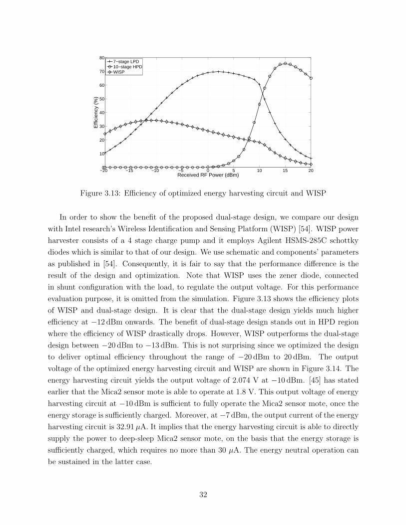
3.13 Efficiency of optimized energy harvesting circuit and WISP . . . . . . . . . . 32
3.14 Output voltage of optimized energy harvesting circuit and WISP . . . . . . . 33
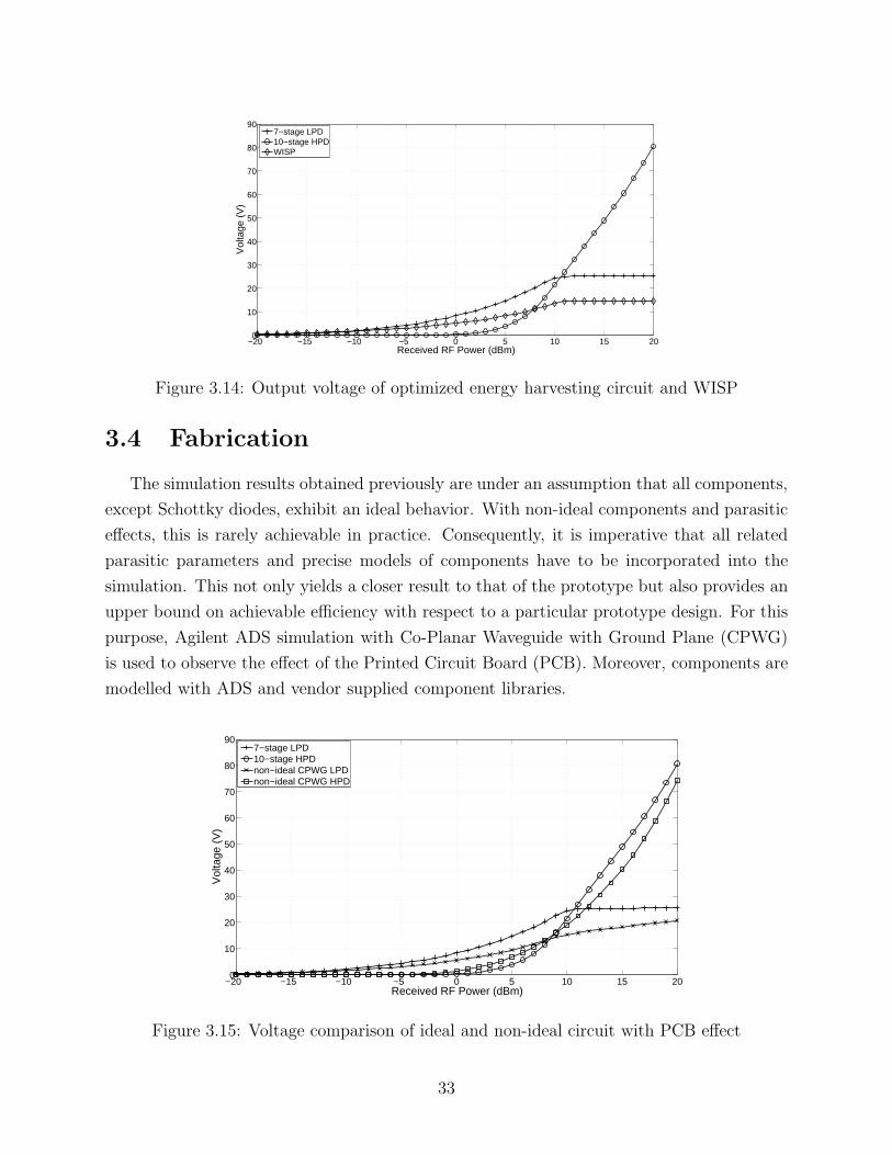
3.15 Voltage comparison of ideal and non-ideal circuit with PCB effect . . . . . . 33
3

3.16 Efficiency comparison of ideal and non-ideal circuit with PCB effect . . . . . 34
3.17 RF energy harvesting with multiple antennas . . . . . . . . . . . . . . . . . . 35
3.18 Effect of multiple antennas on EH circuit’s voltage . . . . . . . . . . . . . . . 35
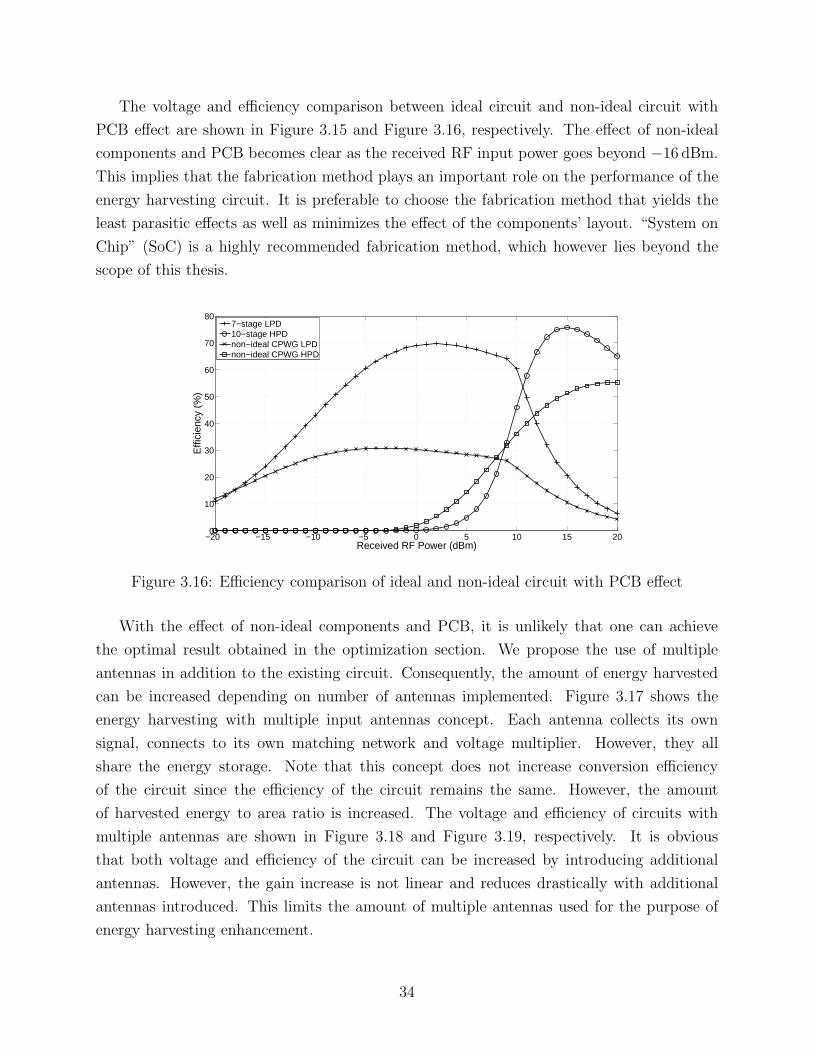
3.19 Effect of multiple antennas on EH circuit’s efficiency . . . . . . . . . . . . . 36
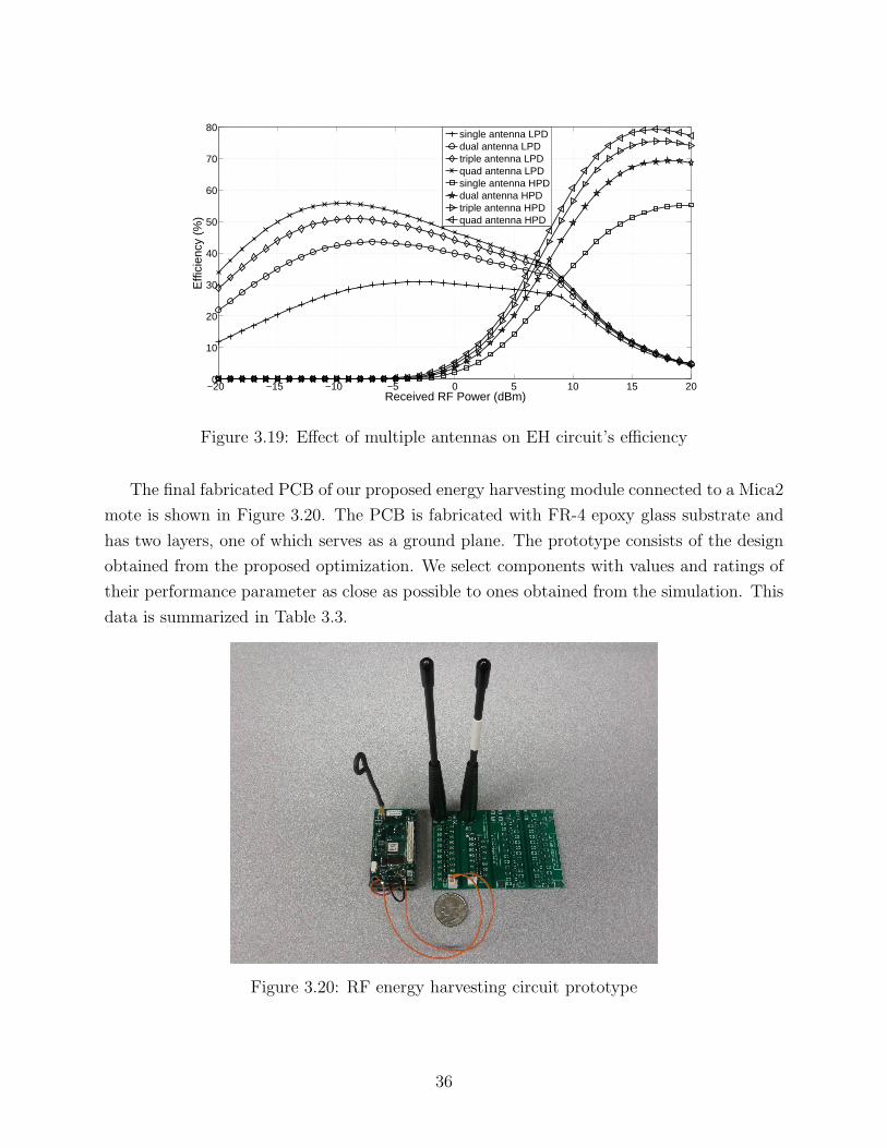
3.20 RF energy harvesting circuit prototype . . . . . . . . . . . . . . . . . . . . . 36
3.21 Output voltage comparisons between -20 dBm and 20 dBm . . . . . . . . . . 38
3.22 Output voltage comparisons between -20 dBm and 5 dBm . . . . . . . . . . 38
3.23 Efficiency comparisons . . . . . . . . . . . . . . . . . . . . . . . . . . . . . . 39
4.1 Agilent N5181 MXG RF Signal Generator . . . . . . . . . . . . . . . . . . . 42
4.2 Agilent 34401A multimeter . . . . . . . . . . . . . . . . . . . . . . . . . . . . 42
4.3 The Wake-up Study harvester circuit prototype . . . . . . . . . . . . . . . . 43
4.4 The combined prototype . . . . . . . . . . . . . . . . . . . . . . . . . . . . . 43
4.5 The experimental setup for wake-up radio . . . . . . . . . . . . . . . . . . . 44
4.6 Voltage output of WISP and power harvesting circuit . . . . . . . . . . . . . 44
4.7 Potential wake-up delay . . . . . . . . . . . . . . . . . . . . . . . . . . . . . 44
4

List of Tables
2.1 Estimated power from various energy harvesting sources . . . . . . . . . . . . 16
3.1 Normalized area at 10.75 dBm crossover point . . . . . . . . . . . . . . . . . . 31
3.2 Optimal solution at various crossover points . . . . . . . . . . . . . . . . . . . 31
3.3 Components used in ADS simulation for Dual-Stage circuit design . . . . . . . 37
3.4 Parameters used in PCB fabrication for Dual-Stage circuit design . . . . . . . 37
4.1 Components used in ADS simulation for circuit design of wake-up radio study 42
4.2 Parameters used in PCB fabrication for circuit design of wake-up radio study 42
4.3 The components used to build the energy harvester . . . . . . . . . . . . . . . 43
5

Chapter 1
Introduction
Energy is a basic necessity for sustaining human life, which pervades each and every one
of our activities. In the very early days, we used muscle power (both human and animals)
to drive simple implements and machines, which could only run for a limited time and had
limitations on their continuous availability. The biggest transition happened when we learnt
to generate energy, by transforming one state of energy, possibly latent, to another. Suddenly,
vast possibilities opened up where energy could be obtained, stored, and transferred across
large distances.
Figure 1.1: Energy demand
As an essential keystone in furthering the reach of technology and a catalyst for economic
development, it is becoming hard to meet the insatiable need of energy today. According
to IEA total world energy supply was 102, 569 TWh (1990); 117, 687 TWh (2000); 133, 602
TWh (2005) and 143, 851 TWh (2008). World power generation was 11, 821 TWh (1990);
6

15, 395 TWh (2000); 18, 258 TWh (2005) and 20, 181 TWh (2008)[13]. The increasing energy
demand puts a strain on current energy sources. Fossil fuels, which comprise a majority of
current output, are being depleted. Other classical sources, such as coal, may result in
adverse environmental effects [6]. As a very recent occurrence, the devastating destruction
of the nuclear plant in Fukushima in Japan has brought about a review and closure of many
similar grade energy generation facilities worldwide [7]. Thus, there is an incessant effort to
identify new sources of energy that may partially satisfy the energy demands and conserve
our finite natural resources for the years to come[8].
Renewable energy sources provide an alternative to conventional natural sources, of which
there are limited supplies. Renewable energy can be broadly defined as a kind of energy that
is generated from natural sources, which is not typically depleted, such as sunlight, wind,
rain, tidal motion, flowing water, biomass, geothermal heat, among others. According to the
International Energy Agency, renewable energy is derived from natural processes that are
replenished constantly [13]. Some additional features of renewable energy sources that make
them an attractive alternative to the classical natural sources are:
• Renewable energy sources are often accessible without geographical and national barri-
ers, though certain regions may be more conducive to their large-scale use (e.g., coastal
regions for tidal energy; countries situated around the equator for solar energy).
• Renewable energy sources generally do not result in harmful by-products of generation,
which adversely affect the environment. Hence, they are very clean and safe to use.
• These sources are inexhaustible in the near term, unlike fossil fuels, which are get-
ting used up faster everyday. They are generally free to harness, though specialized
equipment may be needed for high conversion efficiency.
Figure 1.2: Energy harvesting systems, courtesy of [12]
7
A complete overview of the how energy from different sources is generated, stored and
consumed is given in Figure 1.2. The technique of converting this raw energy source into
useful electrical energy is called as energy harvesting. Quoting the Energy Harvesting Forum,
energy harvesting is the process of capturing minute amounts of energy from one or more of
these naturally-occurring (renewable) energy sources, accumulating them and storing them
for later use [9]. A similar viewpoint is reflected by the industrial sector. According to Dr.
Peter Harrop, the Founder and Chairman of IDTechEx, a large company studying on energy
harvesting and storage, energy harvesting is the conversion of ambient energy into electricity
to drive small or mobile electronic and electrical devices [10]. It is interesting to note that
not all renewable source of energy have equivocal support. Wind power, such as the large
scale deployment in the Cape Cod region in Massachusetts, US, continues to draw the ire of
environmental groups that argue about its detrimental impact on coastal populations [11].
Typically, in commercial energy harvesting systems, the energy harvested from renewable
resources firstly arrives at boost converters that scale up the voltage, followed by battery
management systems where this energy is stored. In this way, it is converted into a useful
and regulated form for many small electronic and mobile applications, such as a wireless
sensor network, depicted in Figure1.3.
Figure 1.3: Energy harvesting systems diagram
As energy harvesting becomes technologically viable, one might wonder what advantages
it has over traditional methods of energy generation and storage. Four advantages of energy
8
harvesting that provide useful clues in this context are [9]:
• The efficiency of the energy harvesting devices has increased with recent technical
developments, especially while capturing energy from ambient sources. Additionally,
power consumption of engineered devices is reducing over time, with advancements in
microprocessor technology. In combination of the above two facts, energy harvesting
is becoming a viable way to drive many low-power applications, potentially replacing
current sources of power in the future.
• Energy harvesting can be a maintenance-free alternative to battery technology, which
is costly and inconvenient to replace. Thus, lifetime of the appliance may be unlimited
if run with well-designed energy harvesting systems. If the source of the energy is
guaranteed to available, energy harvesting systems can be used more reliably than
battery and plug-based connections.
Figure 1.4: The improvements in technology comparing batteries with other devices.
• Energy harvesting can be used as backup generator in power systems, which helps to
improve the reliability and prevent power interruptions.
• Energy harvesting systems can provide mobility to devices, which are dependent on the
traditional plug-based electricity sources. Thus, some wired (cable-driven) applications
9
are transformed into wireless applications.
Energy harvesting systems can be classified according to the source which energy is
harvested from. The most commonly observed energy harvesting systems are based on the
following;
• Mechanical Energy (piezoelectric vibrations, human body movement, etc.)
• Thermal Energy (using geo-thermal energy of the earth, difference in temperatures of
two points of a conductor etc.)
• Light Energy (primarily, solar energy)
• Electromagnetic Energy (mainly from radio frequency waves, magnetic coupling)
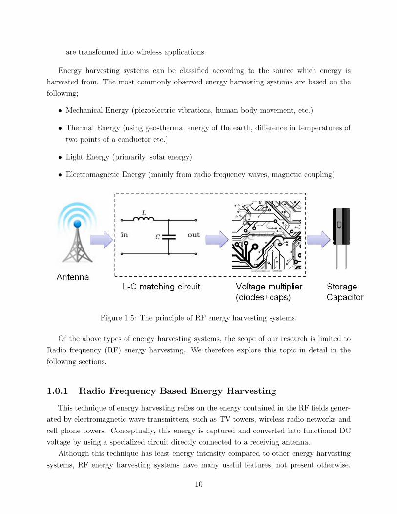
Figure 1.5: The principle of RF energy harvesting systems.
Of the above types of energy harvesting systems, the scope of our research is limited to
Radio frequency (RF) energy harvesting. We therefore explore this topic in detail in the
following sections.
1.0.1 Radio Frequency Based Energy Harvesting
This technique of energy harvesting relies on the energy contained in the RF fields gener-
ated by electromagnetic wave transmitters, such as TV towers, wireless radio networks and
cell phone towers. Conceptually, this energy is captured and converted into functional DC
voltage by using a specialized circuit directly connected to a receiving antenna.
Although this technique has least energy intensity compared to other energy harvesting
systems, RF energy harvesting systems have many useful features, not present otherwise.
10
Such systems can be used in any location that has a high incidence of strong ambient
RF waves, or in specific applications where there is a presence of a dedicated transmitter.
Hence RF energy harvester is generally not dependent on time of the day, geographical
aspects of the region, weather conditions etc., which must be considered in other examples
of energy harvesting systems including solar, and wind energy. RF energy can also be used
to drive more than one device at the same time. For instance, the energy spread from
any omnidirectional transmitter (TV tower, GSM base station etc.) can be scavenged by
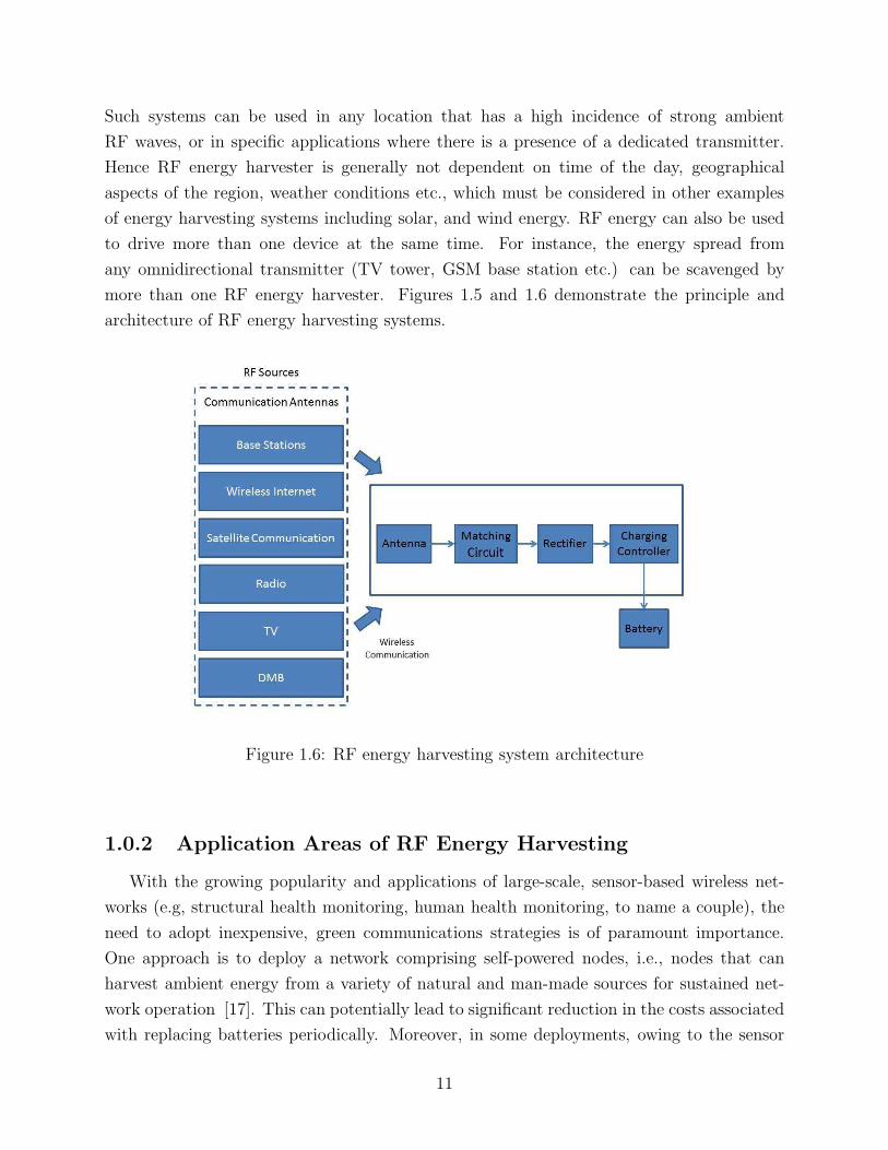
more than one RF energy harvester. Figures 1.5 and 1.6 demonstrate the principle and
architecture of RF energy harvesting systems.
Figure 1.6: RF energy harvesting system architecture
1.0.2 Application Areas of RF Energy Harvesting
With the growing popularity and applications of large-scale, sensor-based wireless net-
works (e.g, structural health monitoring, human health monitoring, to name a couple), the
need to adopt inexpensive, green communications strategies is of paramount importance.
One approach is to deploy a network comprising self-powered nodes, i.e., nodes that can
harvest ambient energy from a variety of natural and man-made sources for sustained net-
work operation [17]. This can potentially lead to significant reduction in the costs associated
with replacing batteries periodically. Moreover, in some deployments, owing to the sensor
11
location, battery replacement may be both practically and economically infeasible, or may
involve significant risks to human life. Thus, there is a strong motivation to enable an off-
the-shelf wireless sensor network (WSN) with energy harvesting capability that would allow
a sensor to replenish part or all of its operational costs, thereby taking the first steps towards
realizing the vision of a perennially operating network.
The concept of wireless energy harvesting and transfer is not new; rather it was demon-
strated over 100 years ago by Tesla [4]. In recent times, RFID technology is a clear example
of wireless power transmission where such a tag operates using the incident RF power emitted
by the transmitter [5]. However, there are limitations in directly porting these approaches
to WSN scenarios: The former cannot be scaled down for the small form factor sensors,
while RFID is unable to generate enough energy to run the local processing tasks on the
node, such as powering the Atmel ATmega128L micro controller on the MICA2 mote [2].
However, given the recent advances in energy efficiency for the circuit components of a sensor
(say, diodes that require less forward voltage threshold), and the low-power operation modes
supported by the device itself (say, sleep mode consuming only W), there is a visible need
for revisiting energy harvesting circuit design that can successfully operate a sensor node.
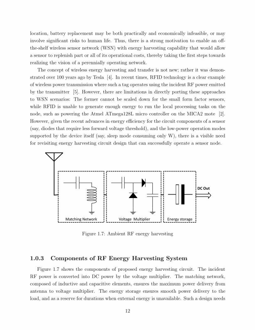
Matching Network Voltage Multiplier Energy storage
DC Out
Figure 1.7: Ambient RF energy harvesting
1.0.3 Components of RF Energy Harvesting System
Figure 1.7 shows the components of proposed energy harvesting circuit. The incident
RF power is converted into DC power by the voltage multiplier. The matching network,
composed of inductive and capacitive elements, ensures the maximum power delivery from
antenna to voltage multiplier. The energy storage ensures smooth power delivery to the
load, and as a reserve for durations when external energy is unavailable. Such a design needs
12

to be carefully crafted: Increasing the number of multiplier stages gives higher voltage at
the load, and yet reduces the current through the final load branch. This may result in
unacceptable charging delays for the energy storage capacitor. Conversely, fewer stages of
the multiplier will ensure quick charging of the capacitor, but the voltage generated across
it may be insufficient to drive the sensor mote (at least 1.8V that becomes the +Vcc for
Mica2 sensors). Along similar lines, a slight change in the matching circuit parameters alters
significantly the frequency range in which the efficiency of the energy conversion is maximum,
often by several MHz. Hence, RF harvesting circuits involve a complex interplay of design
choices, which must be considered together. This problem is addressed by considering a
multi-stage design of the voltage multiplier, whose operating points are decided by solving
an optimization framework.
1.0.4 Thesis Contributions
This thesis summarizes the main contributions of the work as follows:
• Our work demonstrates a circuit design tuned to the unlicensed ISM band at 915MHz1
composed of commonly available off-the-shelf components, such as zero bias Schottky
diodes HSMS-2822 and HSMS-2852 [3], with printed circuit boards (PCBs) that can
be fabricated at marginal costs. This will ultimately result in mass deployment of
harvesting boards along with the sensor nodes.
• This work utilizes a dual-stage design, one that is most efficient at extremely low input
RF power (say, low power design or LPD), and the other at comparatively higher range
(say, high power design or HPD). An optimization framework is developed to decide
the switch-over point between these two sister-circuits so that the fabricated circuit
as a whole delivers the highest achievable efficiency in the operational incident power
range of -20 dBm to 20 dBm.
• Our work achieves the interfacing of proposed circuit with a commonly available Mica2
sensor mote, and then characterizes through experiments, the impact on the duty cycle
of such an integrated device that is powered by harvesting alone.
• Our effort explains how to undertake a rigorous performance evaluation and compare
the design solutions from simulation, under ideal and non-ideal conditions, with the real
PCB fabrication, and also with the state of the art commercially available products in
1The 915MHz ISM band is chosen as it allows direct comparison with the commercial solution fromPowercast [53]
13

terms of efficiency and generated voltage. The non-ideal simulation provides a bound
on achievable efficiency with respect to a particular design.
• The use of multiple input antennas is investigated for increasing the amount of energy
harvested. The simulation result shows that it is feasible, although there exists a bound
on numbers of antennas implemented.
• In addition this work includes another circuit design, composed of same components
with PCBs by using same parameters and design strategies, but interfaced with wireless
identification and sensing platform (WISP), instead of the Mica2 mote. This greatly
improves the wake-up range required by WISP to trigger an interrupt to the Tmote
Sky mote.
The rest of this thesis is organized as follows:
• Chapter 2 gives information about the related work,
• Chapter 3 describes the design, simulation results, measurement and fabrication of
the dual−stage circuit design. Additionally, it gives information about interfacing the
fabricated circuit with MICA2 mote.
• Chapter 4 depicts the design, simulation results, measurement and fabrication of the
circuit design for Wake−up Radio study. Additionally it gives results on using the
fabricated circuit with existing work wake-up radio, to increase its operational range.
• Chapter 5 presents some conclusions and future work.
14

Chapter 2
Related Work
Energy harvesting has been in the focus of the research community in recent years.
The energy harvesting systems can be classified according to energy sources scavenged from
ambient environment as shown in Figure 2.1. Table 2.1 shows the estimated power that
can be harvested from different ambient sources. In this section, various types of energy
harvesting research from both academic and industrial sectors are presented.
Figure 2.1: Potential sources of energy harvesting
Solar energy harvesting is the most promising candidate as a harvesting source, since it
offers the highest energy density, among the other options. Also solar cells are the most
mature and commercially established energy harvesting solution, and are available in a wide
range of sizes and power levels [14][16]. In [17], a solar energy harvesting module is used
to power a sensor mote. Here, the solar energy establishes a topology changing over time
(based on which sensors are currently being powered), where some nodes can receive and
transmit packets without consuming the limited battery resources in [18]. In [19], a solar
energy harvesting scheme which works on the principle of photo-voltaic effect is proposed.
Besides this scheme, a new recharging circuitry, which can reinforce the lifetime of the nodes,
is designed to recharge the battery of the nodes when the charge drops below a threshold
15
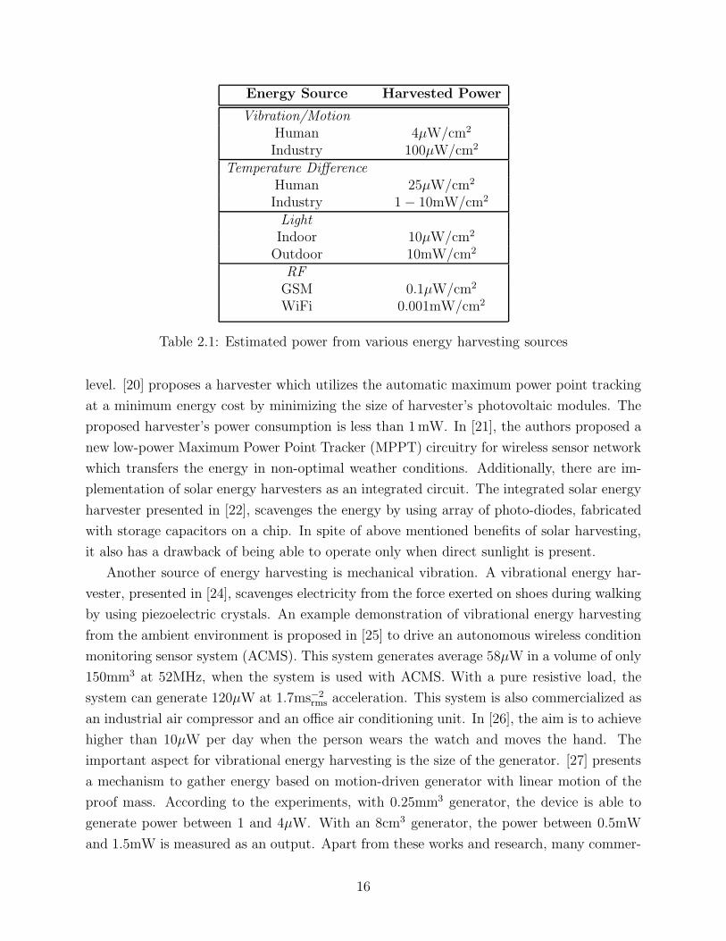
Energy Source Harvested Power
Vibration/MotionHuman 4µW/cm2
Industry 100µW/cm2
Temperature DifferenceHuman 25µW/cm2
Industry 1− 10mW/cm2
LightIndoor 10µW/cm2
Outdoor 10mW/cm2
RFGSM 0.1µW/cm2
WiFi 0.001mW/cm2
Table 2.1: Estimated power from various energy harvesting sources
level. [20] proposes a harvester which utilizes the automatic maximum power point tracking
at a minimum energy cost by minimizing the size of harvester’s photovoltaic modules. The
proposed harvester’s power consumption is less than 1mW. In [21], the authors proposed a
new low-power Maximum Power Point Tracker (MPPT) circuitry for wireless sensor network
which transfers the energy in non-optimal weather conditions. Additionally, there are im-
plementation of solar energy harvesters as an integrated circuit. The integrated solar energy
harvester presented in [22], scavenges the energy by using array of photo-diodes, fabricated
with storage capacitors on a chip. In spite of above mentioned benefits of solar harvesting,
it also has a drawback of being able to operate only when direct sunlight is present.
Another source of energy harvesting is mechanical vibration. A vibrational energy har-
vester, presented in [24], scavenges electricity from the force exerted on shoes during walking
by using piezoelectric crystals. An example demonstration of vibrational energy harvesting
from the ambient environment is proposed in [25] to drive an autonomous wireless condition
monitoring sensor system (ACMS). This system generates average 58µW in a volume of only
150mm3 at 52MHz, when the system is used with ACMS. With a pure resistive load, the
system can generate 120µW at 1.7ms−2rms acceleration. This system is also commercialized as
an industrial air compressor and an office air conditioning unit. In [26], the aim is to achieve
higher than 10µW per day when the person wears the watch and moves the hand. The
important aspect for vibrational energy harvesting is the size of the generator. [27] presents
a mechanism to gather energy based on motion-driven generator with linear motion of the
proof mass. According to the experiments, with 0.25mm3 generator, the device is able to
generate power between 1 and 4µW. With an 8cm3 generator, the power between 0.5mW
and 1.5mW is measured as an output. Apart from these works and research, many commer-
16
cial motion-driven energy harvesters are already being used in industrial applications. These
devices are capable of harvesting in tens of mW [28], [29] with the price of the devices’ size
being proportional to the energy harvested.
Small sensors and on-body devices can also be powered with human body energy harvest-
ing. One of the approaches is to power devices from human body heat. According to [30],
the first thermoelectric device utilizing this concept was demonstrated in 2004. Interuniver-
sity Microelectronics Center (IMC) fabricated a watch-size thermoelectric generator, which
can scavenge energy by using human body heat. The device generates about 100µW under
normal activity. IMEC has also developed a wearable (headphone type) battery-less wire-
less 2-channel electroencephalography (EEG) system, which is powered by heat and ambient
light. This system can generate more than 1mW, on average, in an indoor environment
while consumes only 0.8mW [31]. Recently, the research community has started to focus on
improving efficiency of these thermoelectric devices. In a recent study presented in [32][34],
thermal impedance matching as well as electrical impedance matching are two important
aspects of improving the performance of thermoelectric devices affixed on the human body.
The concept of Wireless Power Transmission (WPT) is not new but was proposed by the
famous scientist Nikola Tesla back in 1899. His experiments with the WPT device consisted
of a massive coil connected to a high mast ball on its top [4]. Based on Tesla’s research, W.C.
Brown introduced and developed the first “rectenna”, which is a type of voltage rectifying
antenna in 1960s. The first experimental results on the rectenna in 1963 reveal an efficiency
of 50% and output 4WDC and 40% at output 7WDC by using 2− 3GHz as the operational
frequency. Moreover, he and his team also developed many devices based on Microwave
Power Transmission (MPT) from 1964 to 1975, such as using MPT in helicopters and design
of further refined rectennas whose efficiencies ranged from 26.5% at 39WDC to 54% at
495WDC with amplitron, an oscillator(or a generator of microwaves) which can amplify a
broad band of microwave frequencies, at 2.45GHz [35].
Recently, many researchers have focused attention on RF energy harvesting, despite its
low energy density. A wireless battery charging system using RF energy harvesting was
studied in [39]. In the study, a cellular phone can be charged with the charging rate of
4mV/second at a frequency of 915MHz. RF energy harvesting with ambient sources is
presented in [40], where the energy harvester can obtain 109µW at 800MHz from daily
office worker’s routine in Tokyo. A new design for remote telemetry based on RF energy
harvesting was proposed in [36]. The design is capable of generating and delivering RF
energy for down-hole telemetry systems ,that is used for monitoring level of underground
water and fossil fuels sources, by using conductive pipes radiating RF signal. Consequently,
the down-hole telemetry systems may be converted to wireless systems with the help of this
design. RF energy harvesting systems are also used with other common energy harvesting
17
systems for some critical life-support purposes. In [37], the authors presented a new harvester
design which is based on a dual-source power scavenging and management system for ultra
low power wireless medical applications. The approach provides a regulated 1.5V as an
output voltage, with a total power consumption of less than 8µW and 48µW in sleep mode
and operating mode, respectively.
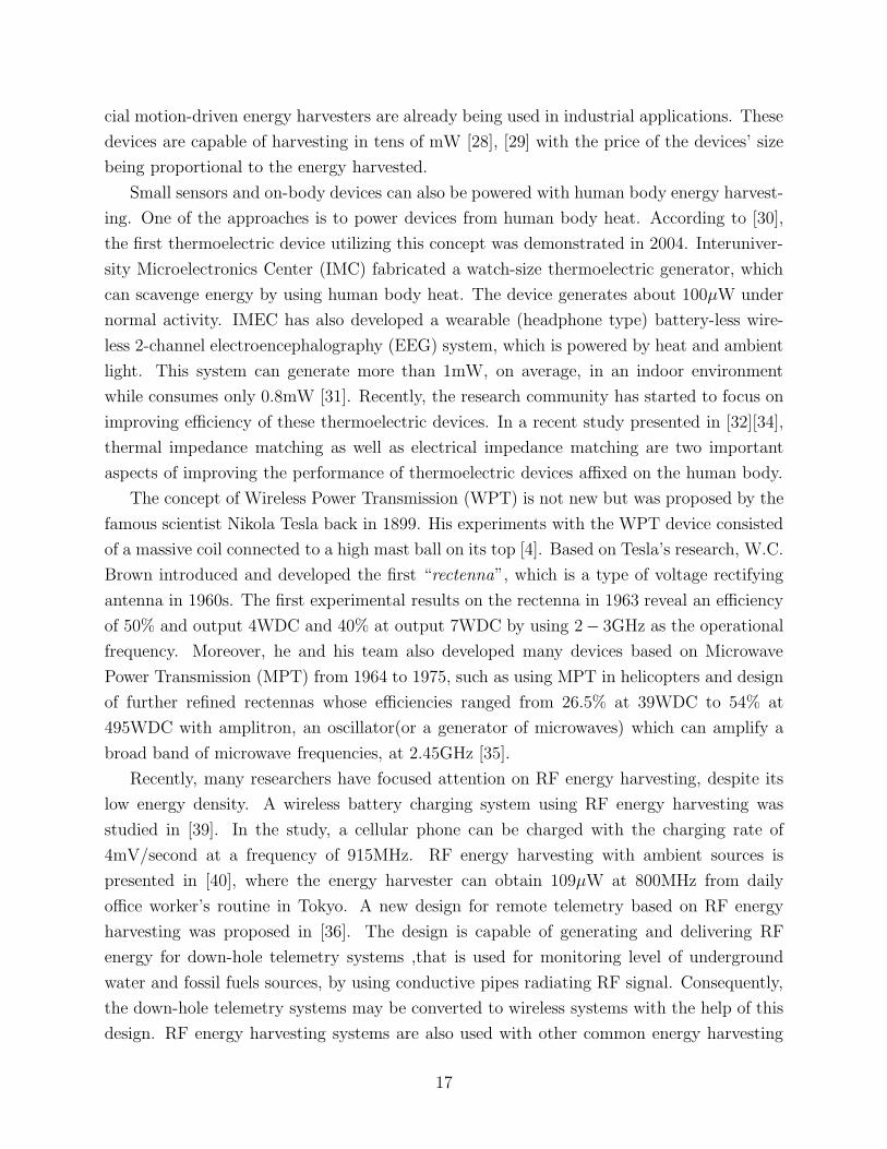
Figure 2.2: Apparatus for ambient RF har-vesting experiment, courtesy of [39]
Figure 2.3: Temperature and humidity meterby using only ambient RF power [39]
In [38], the energy of 60 µW is harvested from TV towers, 4.1 km away, and is able
to operate a small electronic device. The setup is shown in Figures 2.2 and 2.3. Ambient
RF energy harvesting with two systems has been studied in [47]. The first is broadband
system without the impedance matching network while the second is narrow band with the
impedance matching network. The preliminary results indicate that the harvested energy
is not sufficient to directly power the devices, but could be stored for later use. Many
efforts have been focused on the design of RF energy harvesting circuit. In [44] and [48],
an integrated circuit for RF energy harvesting at 868.3MHz, implemented in a Silicon-on-
Glass substrate transfer technology, are presented. The RF-DC power conversion system
was designed in [49], with 0.25µm CMOS technology. At the distance of 15 meters, 1 volt
DC is measured with 0.3µA load current at 906MHz. In addition, the study presented in
[50] mentions the comparison of the performance of voltage multipliers based on CMOS and
Schottky Diode in RF energy harvester.
Common areas where RF energy harvesting concept is utilized include passive radio
18
frequency identification (RFID) and passive RF tags. RFID and RF tags contain a device
powered by propagating RF waves [51]-[52]. In [56], the authors investigate the feasibility and
potential benefits of using passive RFID as a wake-up radio. The results show that using a
passive RFID wake-up radio offers significant energy efficiency benefits at the expense of delay
and the additional low-cost RFID hardware. Recently, prototypes for such RF harvesters
have been developed in the academia [41, 42], as well as commercial products have been
introduced by the industry [53]. However, as we shall show in this thesis, this product
(called as Powercast lifetime power evaluation and development kit) does not perform well
in low power ambient RF environments, where the actual incident power level is 0 dBm and
lower. Consequently, there is a need to develop an energy harvesting circuit that performs
well under these realistic, low power conditions.
+
VRectified
+
VRF
Rectified
RF
Figure 2.4: Villard multiplier
+
-
VRF
+
-
VRectified
Figure 2.5: Dickson multiplier
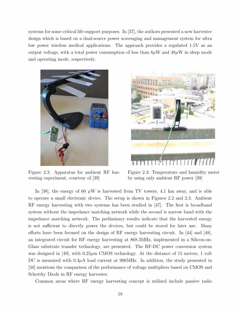
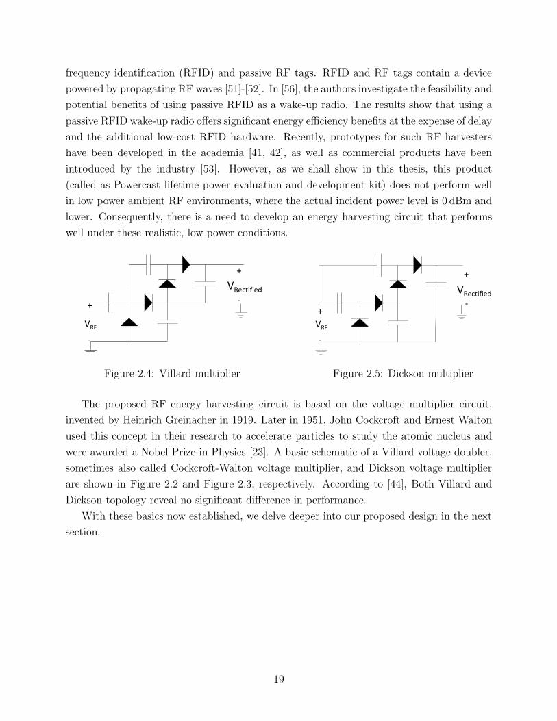
The proposed RF energy harvesting circuit is based on the voltage multiplier circuit,
invented by Heinrich Greinacher in 1919. Later in 1951, John Cockcroft and Ernest Walton
used this concept in their research to accelerate particles to study the atomic nucleus and
were awarded a Nobel Prize in Physics [23]. A basic schematic of a Villard voltage doubler,
sometimes also called Cockcroft-Walton voltage multiplier, and Dickson voltage multiplier
are shown in Figure 2.2 and Figure 2.3, respectively. According to [44], Both Villard and
Dickson topology reveal no significant difference in performance.
With these basics now established, we delve deeper into our proposed design in the next
section.
19
Chapter 3
Dual-Stage RF Energy Harvesting
Circuit
The main challenge faced in harvesting RF energy is the free-space path loss of the
transmitted signal with distance. The Friis transmission equation (3.1) relates the received
(Pr) and transmitted (Pt) powers with the distance R as:
Pr = PtGtGr(λ
4πR)2 (3.1)
where Gt and Gr are antenna gains, and λ is the wavelength of the transmitted signal.
The received signal strength, diminishes with the square of the distance, requires special
sensitivity considerations in the circuit design. Moreover, FCC regulations limit the max-
imum transmission power in specific frequency bands. For example, in the 900MHz band,
this maximum threshold is 4W [43]. Even at this highest setting, the received power at a
moderate distance of 20m is attenuated down to only 10µW. The efficiency of RF energy
harvesting system (in percentages) defined with η is also directly related with rectified power
(Pdc) as well as dependent on received power (Pr) as seen on Equation 3.2.
η =Pdc
Pr
∗ 100 (3.2)
In order to get high efficiency from the energy harvester, the rectifier circuit needs to
be carefully designed by considering all its input parameters. Note that the rectified power
20

is dependent on the rectifier output voltage and current (Pdc = Voutput ∗ Ioutput), and the
number of stages influences greatly both the voltage and current drawn through the load.
In the following sections, we detail the methodology for the new circuit design. We classify
the stages of the work as follows:
• Selection and Effect of the Circuit Components
• Optimization Framework
• Simulation Results
• Fabrication
• Performance Evaluation
3.1 Selection of Circuit Components
Figure 3.1: Block diagram of proposed circuit
As mentioned earlier, the new approach to RF energy harvesting circuit design proposed
in this work is based on the voltage rectifier circuit. In this subsection, we explain how to
select the components of voltage rectifier according to the constraints posed by the load, and
also how the components of circuit influence the efficiency and performance of the circuit.
3.1.1 Choice of Rectifier Topology
As mentioned in [44], the rectifier topologies do not demonstrate a significant difference
in performance. Hence, the Dickson topology (Figure 2.5), which has a parallel configuration
21
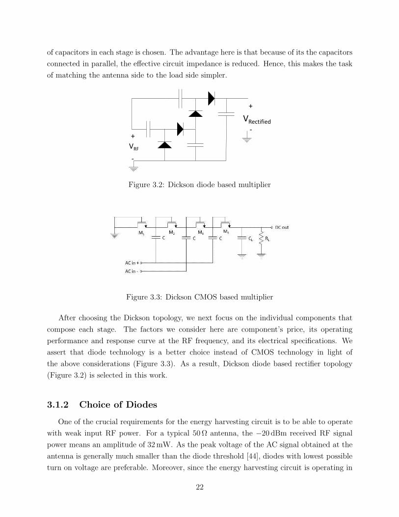
of capacitors in each stage is chosen. The advantage here is that because of its the capacitors
connected in parallel, the effective circuit impedance is reduced. Hence, this makes the task
of matching the antenna side to the load side simpler.
+
-
VRF
+
-
VRectified
Figure 3.2: Dickson diode based multiplier
Figure 3.3: Dickson CMOS based multiplier
After choosing the Dickson topology, we next focus on the individual components that
compose each stage. The factors we consider here are component’s price, its operating
performance and response curve at the RF frequency, and its electrical specifications. We
assert that diode technology is a better choice instead of CMOS technology in light of
the above considerations (Figure 3.3). As a result, Dickson diode based rectifier topology
(Figure 3.2) is selected in this work.
3.1.2 Choice of Diodes
One of the crucial requirements for the energy harvesting circuit is to be able to operate
with weak input RF power. For a typical 50Ω antenna, the −20 dBm received RF signal
power means an amplitude of 32mW. As the peak voltage of the AC signal obtained at the
antenna is generally much smaller than the diode threshold [44], diodes with lowest possible
turn on voltage are preferable. Moreover, since the energy harvesting circuit is operating in
22

high frequencies, diodes with a very fast switching time need to be used. Schottky diodes
use a metal-semiconductor junction instead of a semiconductor-semiconductor junction. This
allows the junction to operate much faster, and gives a forward voltage drop of as low as
0.15V.
Figure 3.4: HSMS-28XX Schottky Diode
We employ 2 different diodes from Avago Technologies, HSMS-2822 and HSMS-2852.
The former has the turn on voltage of 340 mV while the latter is at 150 mV, measured
at 1 mA and 0.1 mA, respectively. Consequently, HSMS-2852 is suitable for low power
design (LPD) used in the weak RF environment, while HSMS-2822 is preferred for high
power design (HPD) in the strong RF environment. Saturation current is another critical
parameter that impacts the efficiency of diodes. It is desirable to have diodes with high
saturation current, low junction capacitance and low equivalent series resistance (ESR).
Moreover, diodes with higher saturation current also yield higher forward current, which
is beneficial for load driving. However, higher saturation current is usually found in larger
diodes, which have higher junction and substrate capacitance. The latter two parameters
can introduce increased power loss, where the benefit of higher saturation current is lost.
3.1.3 Number of Stages
The number of rectifier stages has a major influence on the output voltage of the energy
harvesting circuit. Each stage here is a modified voltage multiplier, arranged in series. The
output voltage is directly proportional to the number of stages used in the energy harvesting
circuit. However, practical constraints force a limit on the number of permissible stages, and
in turn, the output voltage. Here, the voltage gain decreases as number of stages increases
due to parasitic effect of the constituent capacitors of each stage, and finally it becomes
negligible.
23
−20 −15 −10 −5 0 5 10 15 200
10
20
30
40
50
60
70
80
Received RF Power (dBm)
Effi
cien
cy (
%)
1−stage3−stage5−stage7−stage9−stage
Figure 3.5: Effect of number of stages on theefficiency of energy harvesting circuit
−20 −15 −10 −5 0 5 10 15 200
5
10
15
20
25
30
35
Received RF Power (dBm)
Vol
tage
(V
)
1−stage3−stage5−stage7−stage9−stage
Figure 3.6: Effect of number of stages on theoutput voltage of energy harvesting circuit
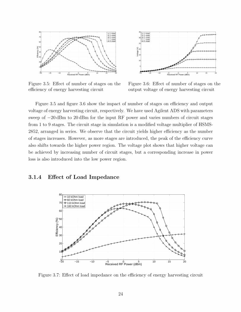
Figure 3.5 and figure 3.6 show the impact of number of stages on efficiency and output
voltage of energy harvesting circuit, respectively. We have used Agilent ADS with parameters
sweep of −20 dBm to 20 dBm for the input RF power and varies numbers of circuit stages
from 1 to 9 stages. The circuit stage in simulation is a modified voltage multiplier of HSMS-
2852, arranged in series. We observe that the circuit yields higher efficiency as the number
of stages increases. However, as more stages are introduced, the peak of the efficiency curve
also shifts towards the higher power region. The voltage plot shows that higher voltage can
be achieved by increasing number of circuit stages, but a corresponding increase in power
loss is also introduced into the low power region.
3.1.4 Effect of Load Impedance
−20 −15 −10 −5 0 5 10 15 200
10
20
30
40
50
60
70
80
Received RF Power (dBm)
Effi
cien
cy (
%)
10 kOhm load60 kOhm load110 kOhm load160 kOhm load
Figure 3.7: Effect of load impedance on the efficiency of energy harvesting circuit
24
It is important that the load impedance is carefully selected for a specific energy harvest-
ing circuit, whose impact on the circuit performance can be seen in Figure 3.7. We simulate
the effect of load impedance on the efficiency of the energy harvesting circuit using Agilent
ADS with parameters sweep of −20 dBm to 20 dBm and 1KΩ to 181KΩ for input RF power
and load value, respectively. We observe that the circuit yields the optimal efficiency at a
particular load value, that is, the circuit’s efficiency decreases dramatically if the load value
is too low or too high. The energy harvesting in simulation is 5-stage circuit, each stage is
a modified voltage multiplier of HSMS-2852, arranged in series.
For the particular case of WSNs, the sensor mote draws a different amount of current
when it in the active (all radios operational), low-power (radios shut down for short interval
but internal micro-controller active), and deep-sleep (requires external interrupt signal to
become active again) states. To correctly identify the impedance in the deep sleep state,
where we presume the node harvests energy, we measure the voltage and current of Mica2
sensor mote in deep sleep state to consume 30 µA at 3.0 V, which translates to a 100KΩ
resistive load. A 100KΩ resistive load is further used in our optimization.
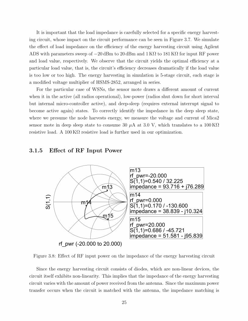
3.1.5 Effect of RF Input Power
rf_pwr (-20.000 to 20.000)
S(1
,1)
m13
m14
m15
m13rf_pwr=S(1,1)=0.540 / 32.225impedance = 93.716 + j76.289
-20.000
m14rf_pwr=S(1,1)=0.170 / -130.600impedance = 38.839 - j10.324
0.000
m15rf_pwr=S(1,1)=0.686 / -45.721impedance = 51.581 - j95.839
20.000
Figure 3.8: Effect of RF input power on the impedance of the energy harvesting circuit
Since the energy harvesting circuit consists of diodes, which are non-linear devices, the
circuit itself exhibits non-linearity. This implies that the impedance of the energy harvesting
circuit varies with the amount of power received from the antenna. Since the maximum power
transfer occurs when the circuit is matched with the antenna, the impedance matching is
25

usually performed at the a particular input power. Figure 3.8 depicts the effect of RF input
power, ranging from −20 dBm to 20 dBm, on the impedance of the energy harvesting circuit.
The non-linearity in operation is shown by a sharp bend at 5 dBm. This further motivates
our approach of a clear separation of two optimized sister-circuits of the LDP and HDP,
where each has its own (reasonably) constant impedance.
3.2 Optimization Framework
The aim of this optimization framework is to maximize the efficiency of the energy har-
vesting module throughout the range of −20 dBm to 20 dBm, subject to several device and
performance constraints. The conversion efficiency is defined in [46] as,
ηc =DC Output Power
Incident RF Power− Reflected RF Power, (3.3)
whereas, the overall efficiency is given by:
ηo =DC Output Power
Incident RF Power(3.4)
Conversion efficiency is defined as a ratio of DC output power of energy harvesting circuit
to net RF input power incident at the input end of the circuit. Consider a plot that measures
the efficiency of the circuit against the input power, also called as the efficiency curve. The
intersection of the two efficiency curves of the LPD (using the HSMS-2852 diode) and HPD
(using the HSMS-2822 diode) circuits, called as the crossover point, splits the overall target
range of −20 dBm to 20 dBm into two.
Conversion efficiency does not take impedance mismatch into the account, and hence re-
flected power is subtracted from received power from the antenna. Consequently, conversion
efficiency is a good parameter to measure the efficiency of only the adaptations we propose
in the voltage multiplier circuit. On the contrary, overall efficiency is defined as a ratio of
DC output power of energy harvesting circuit to incidental RF power at the antenna. It also
includes the effect of reflected RF in the calculation. Therefore, overall efficiency provides
a complete representation of the energy harvesting circuit performance, since matching net-
work is also considered in the efficiency calculation. We use the overall efficiency ηo as the
main performance metric according to this reason, which is the sum of two curves on either
side of the crossover point.
Figure 3.9 shows the two efficiency curves of energy harvesting sister-circuits. The effi-
ciency curves f1(x) and f2(x) belong to LPD and HPD circuits, respectively. The crossover
point, γ, is the point where one of these two circuits become the lead contributor to the
26

Eff
icie
ncy
(%
)
Received RF Power (dBm)
f1(x) f2(x)
Figure 3.9: Efficiency curves of two energy harvesting sister-circuits, for LPD and HPD
total harvested energy. Thus, the LPD is operational if the RF input power is lower than γ,
otherwise the HPD circuit is operational.
As shown in Figure 3.9, there are (β−α)stepsize
potential crossover points between α and β.
At each particular crossover point γ, the total area under efficiency curve is the cumulative
sum of the area under the two distinct efficiency curves corresponding to the LPD and HPD
designs, one on either side of the crossover point γ. The total area under efficiency curve is
hence,
Areatotal =
∫ γ
α
f1(x) dx+
∫ β
γ
f2(x) dx. (3.5)
The crossover point, γ, can be determined as follows:
γ = argmaxγ
∫ γ
α
f1(x) dx+
∫ β
γ
f2(x) dx (3.6)
A problem is said to have an optimal substructure if an optimal solution can be con-
structed efficiently from optimal solutions to its sub-problems. We claim that this optimiza-
tion also exhibits the optimal substructure property. The proof is presented as follows:
lemma :
∫ γ
α
f1(x) dx+
∫ β
γ
f2(x) dx
is maximum then
∫ γ
α
f1(x) dx and
∫ β
γ
f2(x) dxare maximum as well.
(3.7)
proof : if∫ γ
αf1(x) dx and
∫ β
γf2(x) dx were not maximum, then we could substitute∫ γ
αf1(x) dx and
∫ β
γf2(x) dx with larger values and hence obtain an even larger total area,
27

∫ γ
αf1(x) dx+
∫ β
γf2(x) dx.
Furthermore, the efficiency curve is also a function of impedance matching network,
consisting of inductor (L) and capacitor (C). This implies that for each particular crossover
point, there exists more than one efficiency curve. It can be represented in mathematical
form as follows:
∀ α : f(x) = f(L,C) (3.8)
Consequently, the equation 3.6 becomes,
γ = argmaxγ
∫ γ
α
f1(L,C, x) dx+
∫ β
γ
f2(L,C, x) dx (3.9)
Finally, the number of rectifier stages influences the minimum required voltage at the input
in order to obtain a certain output sufficient to drive a sensor mote. We consider various
number of rectifier stages (N), ranging from 1 to 12 stages in this optimization framework.
Hence, the equation 3.9 becomes,
γ = argmaxγ
∫ γ
α
f1(N1, L, C, x) dx+
∫ β
γ
f2(N2, L, C, x) dx (3.10)
We can construct the general optimization framework as follows:
Given : L,C,N
To find : γ,N1, N2 (3.11)
To Maximize :
Areatotal =
∫ γ
α
f1(N1, L, C, x) dx+
∫ β
γ
f2(N2, L, C, x) dx (3.12)
Subject to :∫ γ
α
f1(N1, L, C, x) dx >
∫ β
γ
f1(N1, L, C, x) dx and
∫ β
γ
f2(N2, L, C, x) dx >
∫ γ
α
f2(N2, L, C, x) dx (3.13)
28

∫ β
γ
f2(N2, L, C, x) dx >
∫ γ
α
f2(N2, L, C, x) dx (3.14)
∀ x : I(x+∆x) ≥ I(x) (3.15)
∀ x : V (x+∆x) ≥ V (x) and (3.16)
V (x = −10) ≥ 1.8 V. (3.17)
Figure 3.10: Optimization Constraints
The aim of this optimization framework is to maximize area under the joint efficiency
curve throughout, subject to several constraints which are explained below as seen on Fig-
ure 3.10:
• The efficiency curves of both circuits, one optimized for low input power operation,
i.e., the LPD, and another for high-power operation, i.e. HPD, should not overlap
completely as the effective operational range of the circuit will be adversely impacted.
This is possible by enforcing the constraint on having majority of the area under the
efficiency curve to the left of the crossover point for the LPD circuit, while HPD circuit
has majority of the area to the right of the crossover point.
• Voltage and current should be monotonically increasing. This places a constraint on the
efficiency curve of the energy harvesting circuit to be continuous and without sudden
breaks.
• Finally, the output voltage at −20 dBm ≥ 1.8V. This is to ensure that at the energy
harvesting circuit is operable at the point where it is practically required to drive the
sensor mote in the active state.
29

3.3 Simulation Results
The energy harvesting circuit is simulated using Agilent Advanced Design System (ADS)
software. We use the harmonic balanced analysis (a frequency domain method) in this work
since our objective is to compute the steady state solution of a non-linear circuit. The
alternate method, the so called transient analysis that is undertaken in the time domain is
not used owing to the reason that it must collect sufficient samples for the highest frequency
component. This involves significant memory and processing requirements.
For the optimization framework, we vary the crossover point throughout the target range,
each time evaluating if the overall efficiency is optimized. The number of energy harvesting
stages is varied from 1 to 12 for both LPD and HPD circuits. Moreover, components in
the corresponding matching network are tuned to yield the maximum efficiency for a given
choice of crossover point. We use the input power step size of 0.25 dBm for fine grained
analysis.
In the first study, we keep the crossover point fixed and observe the resulting changes in
the efficiency curves when the number of stages varies, as shown in Figure 3.11. We vary
the number of stages from 5 ,7 and 9 for the LPD, while HPD stages are 8, 10 and 12. The
optimal choice of the circuit stages at a given crossover point is that which maximizes the
overall efficiency ηo. The value of ηo, as well the conversion efficiency area for the two sister-
circuits are shown in Table 3.1. For the LPD, the value of the area under the efficiency curve
increases as the number of stages increases from 5 to 7. However, its peak efficiency reduces
as additional stages are introduced. We observe that the optimal solution for the LPD is
composed of 7-stages. Likewise, 10-stages are found to be best for the HPD. Consequently,
the overall optimal solution, in the rage of −20 dBm to 20 dBm, consists of the pair of 7-stage
LPD circuit and 10-stage HPD circuit.
−20 −15 −10 −5 0 5 10 15 200
10
20
30
40
50
60
70
80
Received RF Power (dBm)
Effi
cien
cy (
%)
5−stage LPD7−stage LPD9−stage LPD8−stage HPD10−stage HPD12−stage HPD
Figure 3.11: Efficiency comparison at 10.75 dBm for different sub-circuit stages
30
Sub-circuit Number of stages/AreaLPD 5-stage/1508.589 7-stage/1550.420 9-stage/1507.892HPD 8-stage/722.535 10-stage/745.355 12-stage/745.222
Table 3.1: Normalized area at 10.75 dBm crossover point
Next, the behavior of the proposed circuit for three different crossover points of 5 dBm,
10.75 dBm and 15 dBm are plotted in Figure 3.12. The optimal solution at 5 dBm crossover
point consists of the pair of 5-stage for the LPD circuit and 10-stages for the HPD circuit.
Similarly, a 9-stage LPD circuit and 8-stage HPD circuit is the optimal solution set at
15 dBm crossover point. During the sweep of the crossover point from the lower input power
end −20 dBm to upper end 20 dBm, we select the optimal solution as one that yields the
maximum ηo. Table 3.2 shows the normalized ηo for various crossover points.
−20 −15 −10 −5 0 5 10 15 200
10
20
30
40
50
60
70
80
90
Received RF Power (dBm)
Effi
cien
cy (
%)
5−stage LPD,5 dBm CP7−stage LPD,10.75 dBm CP9−stage LPD,15 dBm CP10−stage HPD,5 dBm CP10−stage HPD,10.75 dBm CP8−stage HPD,15 dBm CP
Figure 3.12: Optimal efficiency comparison at different crossover
Through an exhaustive search following the constraints of our optimization framework,
we find that the 7-stage LPD circuit and the 10-stage HPD circuit, with the crossover point of
10.75 dBm, yields the maximum ηo, and hence, this is the optimal solution to the framework.
The efficiency curves and the subsequent normalized area values are included in Table 3.2
and Figure 3.12, respectively.
Sub-circuit/Area 5 dBm 10.75 dBm 15 dBmLPD 5-stage/1268.209 7-stage/1550.420 9-stage/1767.046HPD 10-stage/886.416 10-stage/745.355 8-stage/482.067Total area 2154.625 2295.775 2249.122
Table 3.2: Optimal solution at various crossover points
31
−20 −15 −10 −5 0 5 10 15 200
10
20
30
40
50
60
70
80
Received RF Power (dBm)
Effi
cien
cy (
%)
7−stage LPD10−stage HPDWISP
Figure 3.13: Efficiency of optimized energy harvesting circuit and WISP
In order to show the benefit of the proposed dual-stage design, we compare our design
with Intel research’s Wireless Identification and Sensing Platform (WISP) [54]. WISP power
harvester consists of a 4 stage charge pump and it employs Agilent HSMS-285C schottky
diodes which is similar to that of our design. We use schematic and components’ parameters
as published in [54]. Consequently, it is fair to say that the performance difference is the
result of the design and optimization. Note that WISP uses the zener diode, connected
in shunt configuration with the load, to regulate the output voltage. For this performance
evaluation purpose, it is omitted from the simulation. Figure 3.13 shows the efficiency plots
of WISP and dual-stage design. It is clear that the dual-stage design yields much higher
efficiency at −12 dBm onwards. The benefit of dual-stage design stands out in HPD region
where the efficiency of WISP drastically drops. However, WISP outperforms the dual-stage
design between −20 dBm to −13 dBm. This is not surprising since we optimized the design
to deliver optimal efficiency throughout the range of −20 dBm to 20 dBm. The output
voltage of the optimized energy harvesting circuit and WISP are shown in Figure 3.14. The
energy harvesting circuit yields the output voltage of 2.074 V at −10 dBm. [45] has stated
earlier that the Mica2 sensor mote is able to operate at 1.8 V. This output voltage of energy
harvesting circuit at −10 dBm is sufficient to fully operate the Mica2 sensor mote, once the
energy storage is sufficiently charged. Moreover, at −7 dBm, the output current of the energy
harvesting circuit is 32.91µA. It implies that the energy harvesting circuit is able to directly
supply the power to deep-sleep Mica2 sensor mote, on the basis that the energy storage is
sufficiently charged, which requires no more than 30 µA. The energy neutral operation can
be sustained in the latter case.
32
−20 −15 −10 −5 0 5 10 15 200
10
20
30
40
50
60
70
80
90
Received RF Power (dBm)
Vol
tage
(V
)
7−stage LPD10−stage HPDWISP
Figure 3.14: Output voltage of optimized energy harvesting circuit and WISP
3.4 Fabrication
The simulation results obtained previously are under an assumption that all components,
except Schottky diodes, exhibit an ideal behavior. With non-ideal components and parasitic
effects, this is rarely achievable in practice. Consequently, it is imperative that all related
parasitic parameters and precise models of components have to be incorporated into the
simulation. This not only yields a closer result to that of the prototype but also provides an
upper bound on achievable efficiency with respect to a particular prototype design. For this
purpose, Agilent ADS simulation with Co-Planar Waveguide with Ground Plane (CPWG)
is used to observe the effect of the Printed Circuit Board (PCB). Moreover, components are
modelled with ADS and vendor supplied component libraries.
−20 −15 −10 −5 0 5 10 15 200
10
20
30
40
50
60
70
80
90
Received RF Power (dBm)
Vol
tage
(V
)
7−stage LPD10−stage HPDnon−ideal CPWG LPDnon−ideal CPWG HPD
Figure 3.15: Voltage comparison of ideal and non-ideal circuit with PCB effect
33
The voltage and efficiency comparison between ideal circuit and non-ideal circuit with
PCB effect are shown in Figure 3.15 and Figure 3.16, respectively. The effect of non-ideal
components and PCB becomes clear as the received RF input power goes beyond −16 dBm.
This implies that the fabrication method plays an important role on the performance of the
energy harvesting circuit. It is preferable to choose the fabrication method that yields the
least parasitic effects as well as minimizes the effect of the components’ layout. “System on
Chip” (SoC) is a highly recommended fabrication method, which however lies beyond the
scope of this thesis.
−20 −15 −10 −5 0 5 10 15 200
10
20
30
40
50
60
70
80
Received RF Power (dBm)
Effi
cien
cy (
%)
7−stage LPD10−stage HPDnon−ideal CPWG LPDnon−ideal CPWG HPD
Figure 3.16: Efficiency comparison of ideal and non-ideal circuit with PCB effect
With the effect of non-ideal components and PCB, it is unlikely that one can achieve
the optimal result obtained in the optimization section. We propose the use of multiple
antennas in addition to the existing circuit. Consequently, the amount of energy harvested
can be increased depending on number of antennas implemented. Figure 3.17 shows the
energy harvesting with multiple input antennas concept. Each antenna collects its own
signal, connects to its own matching network and voltage multiplier. However, they all
share the energy storage. Note that this concept does not increase conversion efficiency
of the circuit since the efficiency of the circuit remains the same. However, the amount
of harvested energy to area ratio is increased. The voltage and efficiency of circuits with
multiple antennas are shown in Figure 3.18 and Figure 3.19, respectively. It is obvious
that both voltage and efficiency of the circuit can be increased by introducing additional
antennas. However, the gain increase is not linear and reduces drastically with additional
antennas introduced. This limits the amount of multiple antennas used for the purpose of
energy harvesting enhancement.
34

Matching Network Voltage Multiplier
Energy storage
DC Out
.
.
.
Figure 3.17: RF energy harvesting with multiple antennas
−20 −15 −10 −5 0 5 10 15 200
10
20
30
40
50
60
70
80
90
Received RF Power (dBm)
Vol
tage
(V
)
single antenna LPDdual antenna LPDtriple antenna LPDquad antenna LPDsingle antenna HPDdual antenna HPDtriple antenna HPDquad antenna HPD
Figure 3.18: Effect of multiple antennas on EH circuit’s voltage
35
−20 −15 −10 −5 0 5 10 15 200
10
20
30
40
50
60
70
80
Received RF Power (dBm)
Effi
cien
cy (
%)
single antenna LPDdual antenna LPDtriple antenna LPDquad antenna LPDsingle antenna HPDdual antenna HPDtriple antenna HPDquad antenna HPD
Figure 3.19: Effect of multiple antennas on EH circuit’s efficiency
The final fabricated PCB of our proposed energy harvesting module connected to a Mica2
mote is shown in Figure 3.20. The PCB is fabricated with FR-4 epoxy glass substrate and
has two layers, one of which serves as a ground plane. The prototype consists of the design
obtained from the proposed optimization. We select components with values and ratings of
their performance parameter as close as possible to ones obtained from the simulation. This
data is summarized in Table 3.3.
Figure 3.20: RF energy harvesting circuit prototype
36

Component ValueInductor 3.0, 7.12 nHCapacitor 1.5, 2.9 pFStage capacitor 36 pFDiode HSMS-2852, HSMS-2822
Table 3.3: Components used in ADS simulation for Dual-Stage circuit design
The energy harvesting circuit prototype is tuned to match simulation parameters using
Agilent E5061B vector network analyser. In order to measure DC power output from the
prototype, Agilent N5181 MXG RF signal generator is used to provide a known RF power
to the prototype from −20 dBm to 20 dBm. The DC output power from the prototype
is obtained from measuring the voltage and current associated with the resistive load of
100KΩ. The load value representing the Mica2 is so chosen as it is measured in sleep mode
to consume 30 µA at 3.0 V, which translates to a 100KΩ resistive load. We use Agilent
34401A multimeter to measure voltage and current on the resistive load. Our prototype is
fabricated with specifications shown in Table 3.4.
Component ValueLaminate thickness 62 mil FR-4Number of Layers 2-layer, one serves as a ground planeCopper thickness 1.7 milTrace width 20 mil with 12 mil gapDielectric constant 4.6Through-hole size 29 mil
Table 3.4: Parameters used in PCB fabrication for Dual-Stage circuit design
3.5 Performance Evaluation
We describe the efficiency of our fabricated harvesting board, also referred to as prototype,
and compare with the commercially available RF energy harvester from Powercast [53]. We
use P1100 evaluation board for the performance comparison. Powercast P1100 is a high
efficiency RF energy harvesting device that converts received RF energy into DC power.
The voltage and current of Powercast P1100 is measured with the same equipments under
the same external conditions.
Figure 3.21 shows the voltage plot of the non-ideal simulation, prototype and Powercast
P1100 across the load of 100KΩ with −20 dBm to 20 dBm input RF power. It is clear that
the voltage plots of the prototype, both LPD and HPD, are not able to exceed with the
37
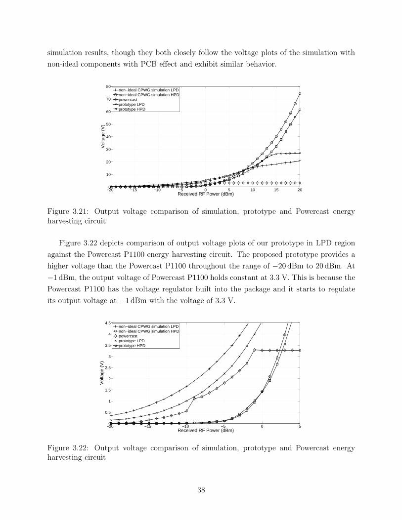
simulation results, though they both closely follow the voltage plots of the simulation with
non-ideal components with PCB effect and exhibit similar behavior.
−20 −15 −10 −5 0 5 10 15 200
10
20
30
40
50
60
70
80
Received RF Power (dBm)
Vol
tage
(V
)
non−ideal CPWG simulation LPDnon−ideal CPWG simulation HPDpowercastprototype LPDprototype HPD
Figure 3.21: Output voltage comparison of simulation, prototype and Powercast energyharvesting circuit
Figure 3.22 depicts comparison of output voltage plots of our prototype in LPD region
against the Powercast P1100 energy harvesting circuit. The proposed prototype provides a
higher voltage than the Powercast P1100 throughout the range of −20 dBm to 20 dBm. At
−1 dBm, the output voltage of Powercast P1100 holds constant at 3.3 V. This is because the
Powercast P1100 has the voltage regulator built into the package and it starts to regulate
its output voltage at −1 dBm with the voltage of 3.3 V.
−20 −15 −10 −5 0 50
0.5
1
1.5
2
2.5
3
3.5
4
4.5
Received RF Power (dBm)
Vol
tage
(V
)
non−ideal CPWG simulation LPDnon−ideal CPWG simulation HPDpowercastprototype LPDprototype HPD
Figure 3.22: Output voltage comparison of simulation, prototype and Powercast energyharvesting circuit
38
−20 −15 −10 −5 0 5 10 15 200
10
20
30
40
50
60
Received RF Power (dBm)
Effi
cien
cy (
%)
non−ideal CPWG simulation LPDnon−ideal CPWG simulation HPDpowercastprototype LPDprototype HPD
Figure 3.23: Efficiency comparison of simulation, prototype and Powercast energy harvestingcircuit
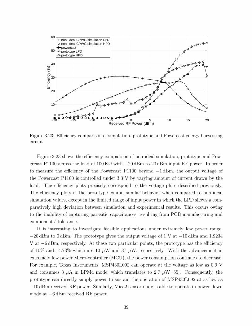
Figure 3.23 shows the efficiency comparison of non-ideal simulation, prototype and Pow-
ercast P1100 across the load of 100KΩ with −20 dBm to 20 dBm input RF power. In order
to measure the efficiency of the Powercast P1100 beyond −1 dBm, the output voltage of
the Powercast P1100 is controlled under 3.3 V by varying amount of current drawn by the
load. The efficiency plots precisely correspond to the voltage plots described previously.
The efficiency plots of the prototype exhibit similar behavior when compared to non-ideal
simulation values, except in the limited range of input power in which the LPD shows a com-
paratively high deviation between simulation and experimental results. This occurs owing
to the inability of capturing parasitic capacitances, resulting from PCB manufacturing and
components’ tolerance.
It is interesting to investigate feasible applications under extremely low power range,
−20 dBm to 0 dBm. The prototype gives the output voltage of 1 V at −10 dBm and 1.9234
V at −6 dBm, respectively. At these two particular points, the prototype has the efficiency
of 10% and 14.73% which are 10 µW and 37 µW, respectively. With the advancement in
extremely low power Micro-controller (MCU), the power consumption continues to decrease.
For example, Texas Instruments’ MSP430L092 can operate at the voltage as low as 0.9 V
and consumes 3 µA in LPM4 mode, which translates to 2.7 µW [55]. Consequently, the
prototype can directly supply power to sustain the operation of MSP430L092 at as low as
−10 dBm received RF power. Similarly, Mica2 sensor node is able to operate in power-down
mode at −6 dBm received RF power.
39

The application of our circuit is not only limited to powering sensors directly but also
trigger charging, energy neutral operation and radio wakeup [56]. In trigger charging op-
eration, the surplus energy beyond sensor’s consumption is accumulated in energy storage,
i.e. super capacitor and rechargeable battery, thus increases the sensor’s lifetime. For exam-
ple, Texas Instruments’ MSP430G2553 [57] in LPM4 mode draws 100 nA at 1.8 V, which
translates to 180 nW. The prototype yields 2.5% efficiency at −20 dBm, which is 250 nW.
In energy neutral operation which the rate of energy consumption is less than or equal to
that of the harvesting, the prototype is able to sustain the energy neutral of MSP430G2553
in LPM4 at −20 dBm. Finally, the energy harvesting circuit can be used to wake up the
sensor node when predetermined signal strength is detected in the proximity. In this case,
the sensor node has its own power source and spends most of the time in power-down mode.
As a result, the sensor’s lifetime is extended with the use of energy harvesting radio wakeup.
With most applications the output power needs to be regulated. However, voltage reg-
ulation may not be of concern under some circumstances. For example, the high voltage
produced by the circuit occurs under the assumption that the sensor is in power-down mode.
Once the sensor wakes up, it draws higher current thus the voltage decreases. With ambient
RF energy harvesting, the input voltage range is limited by the ambient RF, which rarely
exceeds 0 dBm. So it is safe to say the output voltage is bounded and voltage regulator is
not necessary. However, using a voltage regulator to regulate the output to a useful voltage
is recommended for most applications. A simple zener diode, in shunt configuration with
the load, can be used to regulate the output voltage similar to WISP design. Otherwise, a
buck converter with large conversion ratio can be used for this purpose.
40
Chapter 4
RF Energy Harvesting Circuit Design
For Wake-up Radio
This chapter describes the adaptation of our previously designed RF energy harvest-
ing circuit, which works in parallel with the Wireless Identification and Sensing Platform’s
(WISP’s). The WISP acts as the basic wake-up radio, which triggers an interrupt to the
Tmote Sky mote, the main communicating sensor node. The parameters that influence
selection of the circuit components and design strategies for efficiency in performance are
described here2.
Our aim here is to allow our harvesting circuit to enhance the wake-up ability of the WISP,
by increasing the power range. According to data obtained from UoR, this power range is
between −20dBm and 0dBm, which we have already classified earlier as the low power region.
Thus, we select the low power design (LPD) circuit design based on Dickson diode based
rectifier for interfacing with WISP. Along similar lines, we select HSMS-2852 Schottky diode
as the rectifier diode component. We consider 10 stages for circuit to ensure sufficient output
voltage of the circuit to drive the Tmote at 915MHz. The circuit is fabricated on the PCB
according to the data summarized in Tables 4.1 and 4.2.
In order to get high voltage and power from the circuit output, we must consider the
impedance matching between the antenna and the proposed circuit to provide power trans-
mission. The optimization framework here has several points of departure from the earlier
case used in conjunction with the Mica2 mote. The aim of the new optimization framework
would be to maximize the output voltage of the energy harvesting circuit throughout the
2In this study, we collaborate with the research group in Electrical Engineering department at Universityof Rochester (UoR)
41

Component ValueStage capacitor 36 pFDiode HSMS-2852
Table 4.1: Components used in ADS simula-tion for circuit design of wake-up radio study
Component ValueLaminate thickness 62 mil FR-4Number of Layers 2-layer, one serves as a ground planeCopper thickness 1.7 milTrace width 20 mil with 12 mil gapDielectric constant 4.6Through-hole size 29 mil
Table 4.2: Parameters used in PCB fabrica-tion for circuit design of wake-up radio study
range of −20dBm and 0dBm, subject to the constraint that the output voltage value of
circuit should give the peak value exactly at 915MHz, and also it should be continuous and
monotonically increasing.
In the optimization framework, we keep the input RF power fixed and observe the result-
ing changes on the output voltage value while sweeping the inputs frequency of the circuit.
After we determine the frequency at which the output voltage value reaches the peak value,
we add the capacitor and inductor components on the matching network part as series and
parallel, respectively, to change the frequency of the peak response and draw it closer to
915MHz. In order to sweep the frequency and provide the fixed input RF power to circuit,
Agilent N5181 MXG RF signal generator is used (Figure 4.1). We also use a Agilent 34401A
multimeter to measure the output voltage of circuit (Figure 4.2).
Figure 4.1: Agilent N5181 MXG RF SignalGenerator Figure 4.2: Agilent 34401A multimeter
In order to provide power transmission without any waste of energy, we try to determine
the components of an efficient matching network. We vary the value of the capacitor from
0.1pF to 10pF with 0.1pF step size. Similarly, the value of the inductor is changed from 1nH
to 10nH with 1nH step size. We first determine the frequency of peak output voltage with
the unmatched circuit. Thereafter, we add the capacitor or inductor as a series component
by starting from the minimum value from the determined range, and observe how the peak
output voltage changes with the change in the frequency. When we find that the peak voltage
is reached, and this frequency is closer to 915MHz, the component parameters such as value
and type are used as the series component of the matching network.
After selection of the series component, we repeat similar procedure to find the proper
component values for parallel connections of the matching network. These iterations finally
result in the peak voltage being attained at a frequency very close to 915MHz. At this point,
we assume that all components of the matching network are correctly determined. Table 4.3
42
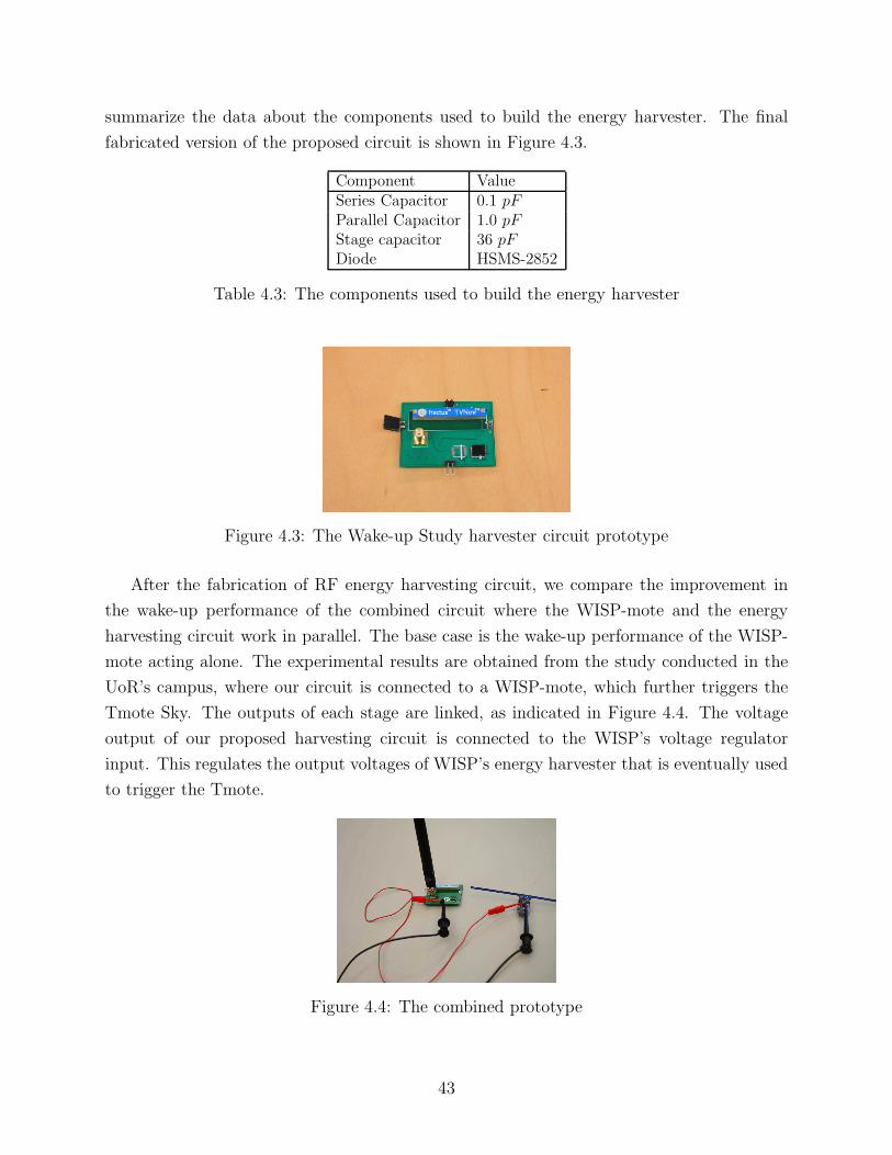
summarize the data about the components used to build the energy harvester. The final
fabricated version of the proposed circuit is shown in Figure 4.3.
Component ValueSeries Capacitor 0.1 pFParallel Capacitor 1.0 pFStage capacitor 36 pFDiode HSMS-2852
Table 4.3: The components used to build the energy harvester
Figure 4.3: The Wake-up Study harvester circuit prototype
After the fabrication of RF energy harvesting circuit, we compare the improvement in
the wake-up performance of the combined circuit where the WISP-mote and the energy
harvesting circuit work in parallel. The base case is the wake-up performance of the WISP-
mote acting alone. The experimental results are obtained from the study conducted in the
UoR’s campus, where our circuit is connected to a WISP-mote, which further triggers the
Tmote Sky. The outputs of each stage are linked, as indicated in Figure 4.4. The voltage
output of our proposed harvesting circuit is connected to the WISP’s voltage regulator
input. This regulates the output voltages of WISP’s energy harvester that is eventually used
to trigger the Tmote.
Figure 4.4: The combined prototype
43
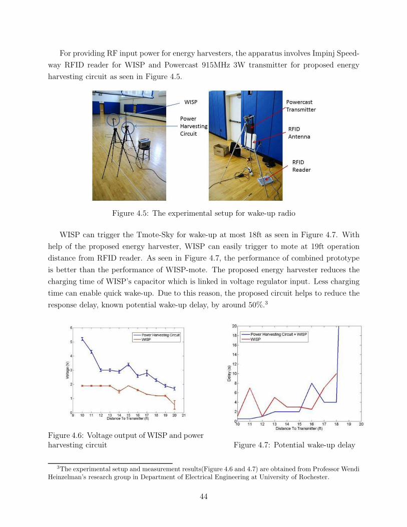
For providing RF input power for energy harvesters, the apparatus involves Impinj Speed-
way RFID reader for WISP and Powercast 915MHz 3W transmitter for proposed energy
harvesting circuit as seen in Figure 4.5.
Figure 4.5: The experimental setup for wake-up radio
WISP can trigger the Tmote-Sky for wake-up at most 18ft as seen in Figure 4.7. With
help of the proposed energy harvester, WISP can easily trigger to mote at 19ft operation
distance from RFID reader. As seen in Figure 4.7, the performance of combined prototype
is better than the performance of WISP-mote. The proposed energy harvester reduces the
charging time of WISP’s capacitor which is linked in voltage regulator input. Less charging
time can enable quick wake-up. Due to this reason, the proposed circuit helps to reduce the
response delay, known potential wake-up delay, by around 50%.3
Figure 4.6: Voltage output of WISP and powerharvesting circuit Figure 4.7: Potential wake-up delay
3The experimental setup and measurement results(Figure 4.6 and 4.7) are obtained from Professor WendiHeinzelman’s research group in Department of Electrical Engineering at University of Rochester.
44

Chapter 5
Conclusion and Future Work
We show that with a simple yet optimal design and optimization, our prototype can yield
almost double the efficiency than that of a major commercially available energy harvesting
circuit in the low incident power range (simulation results for the circuit reveal about 70%
operational efficiency). Our study implies that Mica2 sensor motes can be perpetually op-
erated when their duty-cycle is carefully selected based on the incident RF power (as low
as −6 dBm). Moreover, the prototype is able to sustain the energy neutral of Texas Instru-
ments’ MSP430G2553 in LPM4 at−20 dBm. The experimental results are in good agreement
with the values seen in the non-ideal simulation. We also compare our prototype’s efficiency
with the commercially available RF energy harvester from Powercast, where our prototype
largely outperforms the Powercast P1100 in the range of −20 dBm to 7 dBm.In addition to
dual-stage RF Energy Harvesting Circuit, the prototype designed for Wake-up Radio Study
helps to reduce communication delays between WISP and RFID reader by around 50%. The
harvesting circuit also helps to increase the maximum access point of WISP from 18ft to
19ft. Finally, in order to have a performance improved and lower cost, the circuits need to
be implemented as “System on Chip” as it suffers less above mentioned parasitics, and we
will pursue this in our future work.
45
Bibliography
[1] P. Nintanavongsa, U. Muncuk, D. R. Lewis, K. R. Chowdhury, ”Design Optimization
and Implementation for RF Energy Harvesting Circuits”, JETCAS’12, IEEE Journal
on Emerging and Selected Topics in Circuits and Systems,vol. 2, no. 1, March 2012.
[2] Crossbow Technology, Inc. [Online] http://www.xbow.com/
[3] Avago Technologies, [Online] http://www.avagotech.com
[4] N. Tesla, ”The Transmission of Electric Energy without Wires”, The Thirteenth An-
niversary Number of the Electrical World and Engineer, 1904.
[5] J. Curty, M. Declercq, C. Dehollain, N. Joehl, ”Design and Optimization of Passive UHF
RFID Systems”, Springer,2007.
[6] M. Keating, ”Cradle to Grave: The Environmental Impacts from Coal”, Clean Air Task
Force, June 2001.
[7] P. L. Joskow, J. E. Parsons, ”The Future of Nuclear Power After Fukushima”, CEEPR
WP’12, MIT Center for Energy and Environmental Policy Research, February 2012.
[8] G. Pujare, G. Paranjape, ”Energy Scenario”, Alternative Energy Sources, pp. 1–4 ,
VPM’s Polytechnic, Thane, August 2005.
[9] Energy Harvesting, [Online] http://www.energyharvesting.net/
[10] Energy Harvesting Journal, [Online] http://www.energyharvestingjournal.com/
[11] A. Little, ”Activists Are Split on a Proposed Wind Project off Cape Cod”, [Online]
http://grist.org/article/griscom-windmill/ ,2002.
[12] CNX Software, [Online] http://www.cnx-software.com/2010/11//
[13] IEA Renewable Energy Working Party, ”Renewable Energy”, Renewable Energy into
the mainstream,p. 9, 2002.
46
[14] J. B. Lee, Z. Chen, M. G. Allen, A. Rohatgi, R. Arya, ”A High Voltage Solar Cell Array
As An Electrostatic MEMS Power Supply”, MEMS’94, IEEE Workshop Micro Electro
Mechanical Systems ,pp. 331336, 1994.
[15] D. M. Bennett, R. H. Selfridge, P. Humble, ”Hybrid Power Systems for Autonomous
MEMS”, SPIE’01, Smart Structure and Materials 2001,vol. 4334, pp. 354362, 2001.
[16] K. Sangani, ”Power solar-The Sun in Your Pocket”, Engineering & Technology,vol. 2,
no. 8,pp. 3638, August 2007.
[17] K. Lin, J. Yu, J. Hsu, S. Zahedi, D. Lee, J. Friedman, A. Kansal, V. Raghunathan,
M. Srivastava, ”Heliomote: Enabling Long-Lived Sensor Networks Through Solar En-
ergy Harvesting”, SenSys’05, The 3rd International Conference on Embedded Networked
Sensor Systems, November 2005.
[18] T. Voigt, H. Ritter, J. Schiller, ”Utilizing Solar Power in Wireless Sensor Networks”,
LCN’03, The 28th Annual IEEE International Conference on Local Computer Networks,
October 2003.
[19] R. Balakumar, V. Vaidehi, P. Balamuralidhar, ”Solar Energy Harvesting for Wireless
Sensor Networks”, CICSYN’09, The 1st International Conference on Computational
Intelligence, Communication Systems and Networks, July 2009.
[20] D. Brunelli, L. Benini, C. Moser, L. Thiele, ”An Efficient Solar Energy Harvester for
Wireless Sensor Nodes”, DATE’08, Design, Automation and Test in Europe, March 2008.
[21] C. Alippi, C. Galperti, ”An Adaptive System for Optimal Solar Energy Harvesting
in Wireless Sensor Network Nodes”, Circuits and Systems I: Regular Papers, IEEE
Transactions , July 2008.
[22] N. Guilar, A. Chen, T. Kleeburg, R. Amirtharajah, ”Integrated Solar Energy Harvesting
and Storage”, ISLPED’06, The 2006 International Symposium on Low Power Electronics
and Design, October 2006.
[23] The Nobel Prize in Physics 1951, [Online] http://www.nobelprize.org
[24] J. A. Paradiso, ”Systems for Human-Powered Mobile Computing”, DAC’06, The 43rd
Design Automation Conference, pp.645–650, July 2006.
[25] R. Torah, P. Glynne-Jones, M. Tudor, T. ODonnell, S. Roy, S. Beeby, ”Self-powered
Autonomous Wireless Sensor Node Using Vibration Energy Harvesting”, Measurement
Science and Technology 19, pp. 8, October 2008.
47

[26] M. Hayakawa, ”Electric Wristwatch with Generator”, U.S. Patent, 5 001 685,, March
1991
[27] T. Von Buren, P. D. Mitcheson, T. C. Green, E. M. Yeatman, A. S. Holmes, G. Troster,
”Optimization of Inertial Micropower Generators for Human Walking Motion”, JSEN’06,
IEEE Sensors Journal, vol.6, no. 1, pp. 2838, 2006.
[28] Perpetuum Limited, [Online] http://www.perpetuum.com/
[29] Ferro Solution, [Online] http://www.ferrosi.com/
[30] C. R. V. Leonov, T. Torfs, P. Fiorini, C. Van Hoof, ”Thermoelectric Converters of Hu-
man Warmth for Self-Powered Wireless Sensor Nodes”, JSEN’07, IEEE Sensors Journal ,
vol. 7, pp. 650–657, May 2007.
[31] EE Times India, [Online] http://www.eetindia.co.in
[32] V. Leonov, C. Van Hoof, R. J. M. Vullers, ”Thermoelectric and Hybrid Generators
in Wearable Devices and Clothes”, BSN’09, The 6th International Workshop on Body
Sensors Networks , pp 195200, 2009.
[33] V. Leonov, R. J. M. Vullers, ”Thermoelectric Generators on Living Beings”, ECT’07,
The 5th European Conference on Thermo-electrics , pp 4752, September 2007.
[34] V. Leonov, P. Fiorini, ”Thermal Matching of A Thermoelectric Energy Scavenger with
The Ambience”, ECT’07, The 5th European Conference on Thermo-electrics , pp 129133,
September 2007.
[35] O. A. Campana Escale, ”Study of The Efficiency of Rectifying Antenna Systems for
Electromagnetic Energy Harvesting”, The Degree of Engineer Thesis, Escola Tecnica
Superior d.Enginyeria de Telecomunicacio de Barcelona, Department de Teoria de Senyal
i Comunicacions, Spain, October 2010.
[36] S. D. Briles, D. L. Neagley, D. M. Coates, S. M. Freud, ”Remote Down-hole Well
Telemetry”, U.S. Patent, No. 6766141 B1, July 2004.
[37] Kuan-Yu Lin, Tommy K. K. Tsang, M. Sawan, M. N. El-Gamal, ”Radio-Triggered
Solar and RF Power Scavenging and Management for Ultra Low Power Wireless Medical
Applications”, ISCAS’06, IEEE International Symposium on Circuits and Systems, pp.
5731-5734, 2006.
[38] A. Sample, J. R. Smith, ”Experimental Results with Two Wireless Power Transfer
Systems”, RWS’09, IEEE Radio and Wireless Symposium, 2009.
48

[39] D. W. Harrist, ”Wireless Battery Charging System Using Radio Frequency Energy
Harvesting”, Master of Science Thesis, University of Pittsburgh, USA, 2004.
[40] M. M. Tentzeris, Y. Kawahara, ”Novel Energy Harvesting Technologies for ICT Appli-
cations”, SAINT’08, IEEE International Symposium on Applications and the Internet,
pp. 373–376, 2008.
[41] T. Ungan, L. M. Reindl, ”Harvesting Low Ambient RF-Sources for Autonomous Mea-
surement Systems”, IMTC’08, IEEE International Instrumentation and Measurement
Technology Conference, Victoria, Vancouver Island, Canada, May 2008.
[42] H. Javaheri, G. Noubir, ”iPoint: A Platform-independent Passive Information Kiosk for
Cell Phones”, SECON’10, The 7th Annual IEEE Communications Society Conference
on Sensor Mesh and Ad Hoc Communications and Networks, June 2010.
[43] FCC Codes of Regulation, [Online] http://www.access.gpo.gov/nara/cfr/waisidx03/
[44] H. Yan, J.G. Macias Montero, A. Akhnoukh, L.C.N. de Vreede, J.N. Burghart, ”An
Integration Scheme for RF Power Harvesting”, The 8th Annual Workshop on Semi-
conductor Advances for Future Electronics and Sensors, Veldhoven, Netherlands, 2005.
[45] R. Doost, K. Chowdhury, M. Di Felice, ”Routing and Link Layer Protocol Design
for Sensor Networks with Wireless Energy Transfer”, GLOBECOM’10, IEEE Global
Telecommunications Conference, December 2010.
[46] J. Curty, N. Joehl, C. Dehollain, M. Declercq, ”Remotely Powered Addressable UHF
RFID Integrated System”, JSSC’05, IEEE Journal of Solid-State Circuits, vol.40, no.11,
November, 2005.
[47] D. Bouchouicha, F. Dupont, M. Latrach, L.Ventura, ”Ambient RF Energy Harvesting”,
ICREPQ10, IEEE International Conference on Renewable Energies and Power Quality
, pp. 486–495, March 2010.
[48] H. Yan, M. Popadic, J. G. Macas-Montero, L. C. N. de Vreede, A.
Akhnoukh, L. K. Nanver, ”Design of an RF Power Harvester in a Silicon-
On-Glass Technology”, Delft University of Technology, Netherlands, [Online]
http://www.stw.nl/Programmas/Prorisc/ProRISC+proceedings+2008.htm
[49] T. T. Le, ”Efficient Power Conversion Interface Circuits for Energy Harvesting Appli-
cations”, Doctor of Philosophy Thesis,Oregon State University, USA, 2008.
49

[50] H. Jabbar, Y. S. Song , T. T. Jeong, ”RF Energy Harvesting System and Circuits for
Charging of Mobile Devices”, TCE’10, IEEE Transactions on Consumer Electronics,
vol. 56,issue 1,247-253, February 2010.
[51] K. Finkenzeller, ”RFID Handbook: Fundamentals and Applications in Contactless
Smart Cards and Identification”, Wiley, Chichester, Sussex, U.K., 2003.
[52] A.L. Annala, I. Oy, U. Friedrich, ”Passive Long Distance Multiple Access UHF RFID
System”, Palomar Project, European Commission, Public Report ,Project No. IST1999-
10339, November 2002.
[53] Powercast Corporation, ”P2000 Series 902 − 928MHz Power Harvester Development
Kit”, [Online] http://www.powercastco.com/products/development-kits/
[54] Wireless Identification and Sensing Platform (WISP), [Online]
http://wisp.wikispaces.com/
[55] Texas Instruments MSP430L092, [Online] http://www.ti.com/product/msp430l092
[56] H. Ba, I. Demirkol, W. Heinzelman, ”Feasibility and Benefits of Passive RFID Wake-Up
Radios for Wireless Sensor Networks”, GLOBECOM’10, IEEE Global Telecommunica-
tions Conference, December 2010.
[57] Texas Instruments MSP430G2553, [Online] http://www.ti.com/product/MSP430G2553
50


![Gsm rf-optimization[1]](https://img.pdfslide.net/doc/110x75/555a60dbd8b42a47748b5372/gsm-rf-optimization1.jpg)