Embed Size (px)
Citation preview

March 9, 2006 Dr. Andrew Rawicz School of Engineering Science Simon Fraser University Burnaby, British Columbia V5A 1S6 Re: ENSC 440 – Design Specifications for a Wireless Cell Phone Docking Station Dear Dr. Rawicz: The attached document is the Design Specifications for a Wireless Cell Phone Docking Station from Websa Technology Ltd. We are developing a mobile phone to home phone communication system which allows the user to dock his or her cell phone and use normal corded or cordless home phones to make and receive cellular phone calls. The design specification provides, in detail, the design requirements of our Wireless Docking Station to be achieved at the end of the prototype product in terms of three aspects: architectural overviews, selected components description, and the prototype implementation. The function requirements and test plans for each module stated previously in the Functional Specification for a Wireless Cell Phone Docking Station will be met by this design specification. Websa Technology consists of five talented, innovative, and dedicated fifth-year engineering students: Wilson Kwong (CEO), Andy Leung (CFO), Stephen Au-Yeung (COO), Edwin Wong (CTO-Hardware) and Bobby Ho (CTO-Software). If you have any questions about this document, or the project in general, please feel free to contact us at [email protected]. Thank you. Sincerely, Wilson Kwong Chief Executive Officer Websa Technology Ltd. Enclosure: Design Specifications for a Wireless Cell Phone Docking Station

Design Specifications for a Wireless Cell Phone Docking Station
Copyright © 2006, Websa Technology Ltd. ii

Design Specifications for a Wireless Cell Phone Docking Station
Copyright © 2006, Websa Technology Ltd. iii
Executive Summary Imagine being able to use your cell phone like you would with a normal telephone. Imagine the ability to just pick up the phone and dial without having to worry about poor reception or running out of batteries. Websa Technology Ltd. has the solution with the design of the Wireless Mobile-Dock, a docking station which allows one to dock his/her cell phone and use normal corded or cordless home phones to make and receive cellular phone calls. According to CTIA The Wireless Association for the telecommunications industry, at the end of 2005, wireless subscriptions will have nearly reached 2 billion worldwide [1]. That is, 30.8% of the total world population of approximately 6.5 billion [2] currently uses a wireless subscription service. In the first six months of 2005, total wireless revenues for the US alone was $55.7 Billion USD [1]. The impressive market is made possible by the constantly increasing number of wireless service subscribers. With these numbers, Websa aims to provide wireless subscribers a more comfortable and convenient way to use their cell phones with the introduction of the Wireless Mobile-Dock. The Wireless Mobile-Dock is divided into three critical modules: Base Station Module, Wireless Transmission Module, and Receiver Station Module. The prototype model for each module has its own set of functionalities to satisfy for evaluation purposes. The basic functions of each module are outlined below:
• Base Station Module (BSM): Interface with a docked cell phone to extract necessary signals for transmission to the receiver station module.
• Wireless Transmission Module (WTM):
Transfer, with minimal packet loss, information between BSM and RSM.
• Receiver Station Module (RSM): Provide the interfacing to a normal corded or cordless telephone without generating any loss of user familiarity for telephone systems.
Upon completion of the proof-of-concept prototype (with targeted completion date set for April 2006), the Websa design team will be more equipped to further assess potential marketing ability of the product.
Design Specifications for a Wireless Cell Phone Docking Station
Copyright © 2006, Websa Technology Ltd. iv
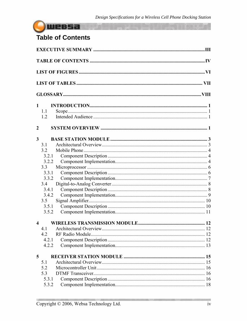
Table of Contents EXECUTIVE SUMMARY ............................................................................................III TABLE OF CONTENTS ............................................................................................... IV LIST OF FIGURES ........................................................................................................VI LIST OF TABLES ........................................................................................................ VII GLOSSARY..................................................................................................................VIII 1 INTRODUCTION................................................................................................. 1
1.1 Scope................................................................................................................... 1 1.2 Intended Audience .............................................................................................. 1
2 SYSTEM OVERVIEW ........................................................................................ 1 3 BASE STATION MODULE ................................................................................ 3
3.1 Architectural Overview....................................................................................... 3 3.2 Mobile Phone ...................................................................................................... 4 3.2.1 Component Description .................................................................................. 4 3.2.2 Component Implementation............................................................................ 4
3.3 Microprocessor ................................................................................................... 6 3.3.1 Component Description .................................................................................. 6 3.3.2 Component Implementation............................................................................ 7
3.4 Digital-to-Analog Converter............................................................................... 8 3.4.1 Component Description .................................................................................. 8 3.4.2 Component Implementation............................................................................ 9
3.5 Signal Amplifier................................................................................................ 10 3.5.1 Component Description ................................................................................ 10 3.5.2 Component Implementation.......................................................................... 11
4 WIRELESS TRANSMISSION MODULE....................................................... 12
4.1 Architectural Overview..................................................................................... 12 4.2 RF Radio Module.............................................................................................. 12 4.2.1 Component Description ................................................................................ 12 4.2.2 Component Implementation.......................................................................... 13
5 RECEIVER STATION MODULE ................................................................... 15
5.1 Architectural Overview..................................................................................... 15 5.2 Microcontroller Unit ......................................................................................... 16 5.3 DTMF Transceiver............................................................................................ 16 5.3.1 Component Description ................................................................................ 16 5.3.2 Component Implementation.......................................................................... 18

Design Specifications for a Wireless Cell Phone Docking Station
Copyright © 2006, Websa Technology Ltd. v
5.4 Digital to Analog Converter.............................................................................. 18 5.5 Telephone Line Interface .................................................................................. 19 5.5.1 Component Description ................................................................................ 19 5.5.2 Component Implementation.......................................................................... 21
5.6 Call Progress Generator .................................................................................... 22 5.6.1 Component Description ................................................................................ 22 5.6.2 Component Implementation.......................................................................... 23
5.7 Ring Voltage Generator .................................................................................... 24 5.7.1 Component Description ................................................................................ 24 5.7.2 Component Implementation.......................................................................... 24
6 SYSTEM EVENT FLOW .................................................................................. 25
6.1 Base Station Module ......................................................................................... 25 6.1.1 Idle State ....................................................................................................... 25 6.1.2 Incoming Call Connection ............................................................................ 25 6.1.3 Outgoing Call Connection ............................................................................ 26 6.1.4 Voice Communication .................................................................................. 27
6.2 Wireless Transmission Module......................................................................... 28 6.2.1 Time Division Multiplexing ......................................................................... 28 6.2.2 Program Flow................................................................................................ 29
6.3 Receiver Station Module................................................................................... 31 6.3.1 Incoming Call Event Flow............................................................................ 31 6.3.2 Outgoing Call Event Flow ............................................................................ 31 6.3.3 Voice Communication .................................................................................. 32
7 CONCLUSION ................................................................................................... 33 8 REFERENCES.................................................................................................... 34 9 APPENDIX.......................................................................................................... 36

Design Specifications for a Wireless Cell Phone Docking Station
Copyright © 2006, Websa Technology Ltd. vi
List of Figures Figure 2-1: Functional interaction between modules.......................................................... 2 Figure 3-1: Architectural Overview of Base Station Module. ............................................ 3 Figure 3-2: Sony Ericsson T310 Mobile Phone.................................................................. 4 Figure 3-3: 11-pin Data Port Connector. ............................................................................ 4 Figure 3-4: Pin Diagram of PIC16F877A Microprocessor................................................. 6 Figure 3-5: Crystal/Ceramic Resonator Operation Circuit. ................................................ 7 Figure 3-6: Recommended Master Clear pin Circuit.......................................................... 7 Figure 3-7: Basic Microcontroller Implementation Diagram. ............................................ 8 Figure 3-9: Unipolar Binary Operation Circuit. ................................................................. 9 Figure 3-10: Pin Diagram of LM324 Operational Amplifier. .......................................... 10 Figure 3-11: Audio Signal Amplifier Circuit.................................................................... 11 Figure 4-1: Overview of WTM as bridging device. ......................................................... 12 Figure 4-2: CC1100EM Wireless Transceiver ................................................................. 12 Figure 4-3: Block diagram to illustrate connection between radio and MCU.................. 13 U
Figure 4-4: CC1100 registers read / write operation ........................................................ 14 Figure 4-5: Packet format ................................................................................................. 14 Figure 5-1: Architectural Overview of Receiver Station Module .................................... 15 Figure 5-2: MT8880CE Pin Connections. ........................................................................ 16 Figure 5-3: MT8880CE Single Ended Input Configuration (μP = Microprocessor, i.e.
MCU). ....................................................................................................................... 18 Figure 5-4: MH88435AD Pin Configuration.................................................................... 19 Figure 5-5: MH88435AD Functional Block Diagram...................................................... 19 Figure 5-6: MH88435AD Application Circuit. ................................................................ 21 Figure 5-7: M991 Pin Assignments .................................................................................. 22 Figure 5-8: M991 Block Diagram..................................................................................... 22 Figure 5-9: Circuit diagram for ringer voltage generator using switching supply. .......... 24 Figure 6-1: Flow Chart of Incoming Call Algorithm........................................................ 26 Figure 6-2: Flow Chart of Outgoing Call Algorithm........................................................ 27 Figure 6-3: Base and receiver TDD receive and transmit mode switching scheme.
Horizontal axis represents the time axis. .................................................................. 28 Figure 6-4: Base and receiver TDD event flow during a voice call. Vertical axis
represents the time axis. Voice packet payload is 10ms of voice data in this case for example purposes...................................................................................................... 29
Figure 6-5: Flow chart of the wireless module program flow. ......................................... 30 Figure 6-6: RSM incoming call event flow. ..................................................................... 31 Figure 6-7: RSM outgoing call event flow. ...................................................................... 32

Design Specifications for a Wireless Cell Phone Docking Station
Copyright © 2006, Websa Technology Ltd. vii
List of Tables Table 3-1: Pin Function Description................................................................................... 4 Table 3-2: Attention Commands list................................................................................... 5 Table 3-3: Status Indications in DCE Response Mode....................................................... 5 Table 3-4: Status Indications of Call Monitoring. .............................................................. 6 Table 3-5: Pin Function Description................................................................................... 9 Table 3-6: Unipolar Binary Operation.............................................................................. 10 Table 5-1: Functional Encode/Decode ( 0 = Logic Low, 1 = Logic High) ...................... 16 Table 5-2: MT8880CE Pin Descriptions. ......................................................................... 17 Table 5-3: MH88435 Pin Descriptions. ............................................................................ 20 Table 5-4: M991 Pin Functions ........................................................................................ 22 Table 5-5: M991 Data/Tone Selection.............................................................................. 23 Table 5-6: Standard Call Progress Tones.......................................................................... 23 Table 9-1: Base Station Module Data Packet Format....................................................... 36 Table 9-2: Bit Representation of Status and States........................................................... 36 Table 9-3: 8-bits Binary Representation of Cell Phone Status ......................................... 36 Table 9-4: 8-bits Binary Representation of Base Station Module State ........................... 36

Design Specifications for a Wireless Cell Phone Docking Station
Copyright © 2006, Websa Technology Ltd. viii
Glossary ADC Analog-to-Digital ATMS Audio to Mobile AFMS Audio from Mobile BSMS Base Station Module State BSM Base Station Module CPG Call Progress Generator CS Cell-Phone Status DAA Data Access Arrangement DAC Digital-to-Analog DIP Dual in-line package DS Dialing String DTMF Dual-Tone Multi-Frequency FIFO First in First Out GBW Gain-Bandwidth Product IC Integrated Circuit ISM Industrial, Scientific, and Medical ITU International Telecommunication Union MCU Microcontroller Unit MIB Module Indication Bit MISO Master In Slave Out MOSI Master Out Slave In PCB Printed Circuit Board PDIP Plastic In-line Dual Package RF Radio Frequency RSM Receiver Station Module RX Receive SCLK SPI Clock SMPI Smart Mobile-to-Phone Interface SPI Serial Peripheral Interface SRD Short Range Device SS Slave Select TDD Time Division Duplex TX Transmit UART Universal Asynchronous Receiver-Transmitter

Design Specifications for a Wireless Cell Phone Docking Station
Copyright © 2006, Websa Technology Ltd. 1
1 Introduction
2
The Wireless Mobile-Dock (WMD) system is a wireless cell phone docking station that provides users the ability to make outgoing and receive incoming cellular phone calls via the use of a normal corded or cordless telephone. The WMD system will help users maximize comfort, convenience and efficiency while engaging in conversations over their cell phones. In addition, the WMD system can potentially lower monthly expenses for the user through the possible elimination of a telephone land line. The intended completion date of the WMD system is April 2006, where the final prototype will satisfy the minimum requirements previously stated in Websa’s Functional Specification for a Wireless Cell Phone Docking Station. 1.1 Scope This document describes the design specifications that must be met by Websa Technology’s Wireless Mobile-Dock system. It also explains how the design will meet the functional requirements set out for the system. The design specifications are written for the implementation of the proof-of-concept models only, as described in our Functional Specifications [3]. The development for the WMD system is broken down into three sub-modules: the base station module (BSM), the receiver station module (RSM) and the wireless transmission module (WTM). 1.2 Intended Audience This design specification is intended for use by all members of Websa Technology Ltd., and is intended to ensure that the WMD System developed by Websa meets all specified requirements. In addition, this document may serve as a tool for marketing to arrange various sales strategies in the future.
System Overview Websa’s Wireless Mobile Dock consists of three main modules: the Base Station module (BSM), Wireless Transmission module (WTM) and Receiver Station module (RSM). Figure 2-1 shows the functional interaction between the modules. Note that the WTM module is embedded into both the BSM and RSM. General module descriptions and system operation are given as followed. The BSM is responsible for providing cell phone docking and interfacing capability. It will constantly monitor the cell phone status and upon receiving an incoming cell phone call interrupt, the BSM will send a notification to the RSM via the Smart Mobile to Phone Interface (SMPI). Signals from the SMPI are relayed by the WTM. The RSM, upon receiving notification of an incoming call, will attempt to ring the telephone. When the telephone is picked up, the RSM will notify the BSM and the BSM will request the cell phone to begin delivering the voice signals. As soon as the WTM streams the voice signals, a
Design Specifications for a Wireless Cell Phone Docking Station
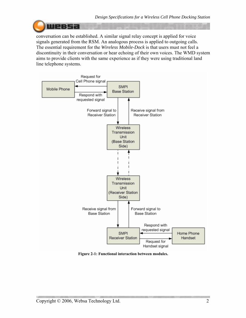
conversation can be established. A similar signal relay concept is applied for voice signals generated from the RSM. An analogous process is applied to outgoing calls. The essential requirement for the Wireless Mobile-Dock is that users must not feel a discontinuity in their conversation or hear echoing of their own voices. The WMD system aims to provide clients with the same experience as if they were using traditional land line telephone systems.
Figure 2-1: Functional interaction between modules.
Copyright © 2006, Websa Technology Ltd. 2

Design Specifications for a Wireless Cell Phone Docking Station
Copyright © 2006, Websa Technology Ltd. 3
3 Base Station Module 3.1 Architectural Overview The base station module (BSM), as shown in Figure 3-1, consists of four individual components: a docked mobile phone, a microprocessor, a Digital-to-Analog converter (DAC), and a signal amplifier. The BSM is responsible for controlling the mobile phone, monitoring the mobile phone’s status, and receiving/transmitting command and audio signals between the mobile phone and the wireless transmission module (WTM). A microprocessor (PIC16F877A) connects the BSM together with the WTM. Thus, the microprocessor behaves as the bridge of the communication between the mobile phone and the wireless transmission unit. Due to the specification of the WTM, all signals are transmitted in a digitized package format only and the MCU will be responsible for digitizing the incoming audio signals from the mobile phone using its own built in Analog-to-Digital converter (ADC). In addition, a DAC device is required for recovering the digitized audio signal sent from the receiver station module (RSM) thru the WTM. The signal amplifier is used to amplify the low-voltage output from the mobile phone data-port to match the dynamic range of the ADC. The following figure is a block diagram of the architectural overview of the BSM.
Mobile Phone Data out Micro-processor
Signal Amplifier
Audio out
DAC
Audio in
Master out Slave in
Master in Slave out
Clock
Chip Select
WirelessTransmission
Unit
Figure 3-1: Architectural Overview of Base Station Module.

Design Specifications for a Wireless Cell Phone Docking Station
3.2 Mobile Phone 3.2.1 Component Description A Sony Ericsson T310 mobile phone (Figure 3-2 [4]) is used for the prototype model development due to the ease of communication establishment with the mobile phone through its data port. A serial data cable is utilized to establish the communication between the data port and the microprocessor’s I/O pins. The mobile phone’s data port layout is shown in Figure 3-3 [5] with the pin assignment and their corresponding descriptions presented in Table 3-1 [5].
Figure 3-2: Sony Ericsson T310
Mobile Phone.
Figure 3-3: 11-pin Data Port
Connector.
Table 3-1: Pin Function Description.
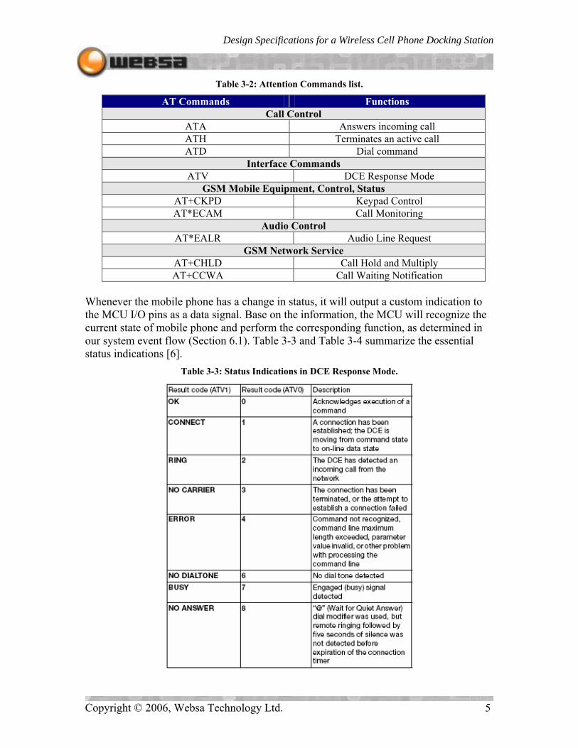
The four most important pins are pins 1, 2, 4, and 5, which represent the Audio to Mobile (ATMS), Audio from Mobile/RTS (AFMS), Data to Mobile (data in) and Data from Mobile (data out), respectively. They are the core pins for communication between the mobile phone and the BSM for voice and data signals. The data in/out pins are directly connected to the MCU I/O pins because the signals do not need to be processed in any way. The ATMS pin will need to pass thru the DAC before entering the data port while the AFMS will first go through a signal amplifier to match the dynamic range of the MCU’s ADC as previously stated. 3.2.2 Component Implementation The MCU controls and monitors the mobile phone’s status thru Attention commands (AT commands) that requests the mobile phone to perform certain functions. Table 3-2 lists the AT commands used for controlling the mobile phone [6].
Copyright © 2006, Websa Technology Ltd. 4
Design Specifications for a Wireless Cell Phone Docking Station
Table 3-2: Attention Commands list.
AT Commands Functions Call Control
ATA Answers incoming call ATH Terminates an active call ATD Dial command
Interface Commands ATV DCE Response Mode
GSM Mobile Equipment, Control, Status AT+CKPD Keypad Control AT*ECAM Call Monitoring
Audio Control AT*EALR Audio Line Request
GSM Network Service AT+CHLD Call Hold and Multiply AT+CCWA Call Waiting Notification
Whenever the mobile phone has a change in status, it will output a custom indication to the MCU I/O pins as a data signal. Base on the information, the MCU will recognize the current state of mobile phone and perform the corresponding function, as determined in our system event flow (Section 6.1). Table 3-3 and Table 3-4 summarize the essential status indications [6].
Table 3-3: Status Indications in DCE Response Mode.
Copyright © 2006, Websa Technology Ltd. 5

Design Specifications for a Wireless Cell Phone Docking Station
Table 3-4: Status Indications of Call Monitoring.
3.3 Microprocessor 3.3.1 Component Description The microprocessor selected is Microchip’s PIC16F877A, which consists of a 40-pin plastic dual in-line package (PDIP). The pin diagram of the microcontroller is shown in the Figure 3-4 [7].
Figure 3-4: Pin Diagram of PIC16F877A Microprocessor.
This specific microprocessor is selected because of its versatility and ease of implementation and programmability. It operates at an incredibly high speed, approximately 200ns, in executing an instruction with a fast settling time of 1.6µs per bit for the ADC module. Its large number of I/O pins is also an advantage for the implementation of the UART interface, the ADC, and the wireless transmission unit. In addition, the chip has potential for higher utilization for future features of the system.
Copyright © 2006, Websa Technology Ltd. 6

Design Specifications for a Wireless Cell Phone Docking Station
The PIC16F877A is powered by 5V DC [7], while an external crystal oscillator (at 20MHz) is required to operate the microprocessor clock. A recommended implementation of the external crystal oscillator is shown in Figure 3-5, where C1 and C2 should be between 15 to 33 pF because of the high speed operation. RS is not required as we are not using strip cut crystal oscillators [7].
Figure 3-5: Crystal/Ceramic Resonator Operation Circuit.
Another manufacturer recommended circuit is implemented at the input to the Master Clear pin. This circuit, shown in Figure 3-6, prevents the voltage input to the pin from exceeding its specified maximum, which will result in both a Reset and current consumption outside of device specification [7].
Figure 3-6: Recommended Master Clear pin Circuit.
Assembly programs can be loaded onto the microprocessor via the MPLAB ICD2 or the PICSTART Plus development application.
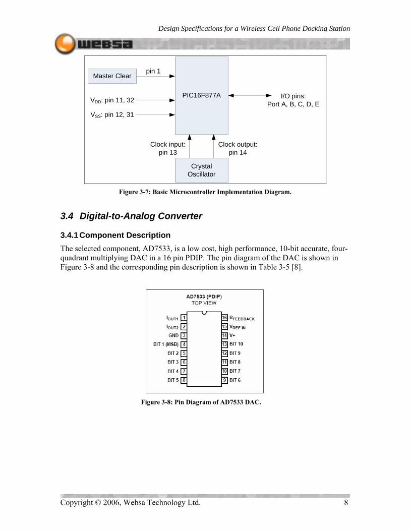
3.3.2 Component Implementation As shown in Figure 3-4, the PIC16F877A microprocessor contains two sets of voltage supply pins, VDD and VSS. VDD is connected to +5V DC, and VSS is connected to ground for proper operation. As illustrated in Figure 3-5, a crystal oscillator is connected to pin 13 and 14, which are the oscillator input and output, respectively. A recommended circuit is connected to pin 1 which is the master clear, as illustrated in Figure 3-6. The remaining I/O pins are used for I/O interfacing with the SPI interface, ADC I/O, and UART I/O, which are all program controlled. At the current stage, we have not fully specified which pins will be responsible for which particular interface. However, a high level implementation block diagram is shown in Figure 3-7.
Copyright © 2006, Websa Technology Ltd. 7
Design Specifications for a Wireless Cell Phone Docking Station
PIC16F877AVDD: pin 11, 32
VSS: pin 12, 31
Master Clear
Crystal Oscillator
pin 1
Clock input: pin 13
Clock output: pin 14
I/O pins: Port A, B, C, D, E
Figure 3-7: Basic Microcontroller Implementation Diagram.
3.4 Digital-to-Analog Converter 3.4.1 Component Description The selected component, AD7533, is a low cost, high performance, 10-bit accurate, four-quadrant multiplying DAC in a 16 pin PDIP. The pin diagram of the DAC is shown in Figure 3-8 and the corresponding pin description is shown in Table 3-5 [8].
Figure 3-8: Pin Diagram of AD7533 DAC.
Copyright © 2006, Websa Technology Ltd. 8

Design Specifications for a Wireless Cell Phone Docking Station
Table 3-5: Pin Function Description.
The advantages of the AD7533 are its sufficiency in digital input pins and its high speed settling time (approximately 150ns). The AD7533 operates between 5V to 15V DC and provides proper binary scaling for reference inputs of either positive or negative polarity. The minimum input high voltage (VINH) level is 2.4V, whereas the maximum input low voltage (VINL) level is 0.8V max. The maximum input reference voltage (VREF) is ±25V. 3.4.2 Component Implementation The AD7533 DAC is a current outputting device; an external operational amplifier is needed to convert the current into voltage. The output voltage stream is then the required analog voice signal. This combination, DAC and op-amp, is called a unipolar binary operation circuit (shown in Figure 3-9 [8]), where the common LM324 is selected as the operational amplifier component.
Figure 3-9: Unipolar Binary Operation Circuit.
Table 3-6 shows several examples of the output voltage level corresponding to its respective digital input value. As listed, when all input bits are active high, the output is equal to the negative of the reference voltage [8]. Conversely, when all inputs are active
Copyright © 2006, Websa Technology Ltd. 9

Design Specifications for a Wireless Cell Phone Docking Station
low, the output is equal to zero. The output is a negative of the reference voltage because the LM324 is acting as an inverting op-amp in this design.
Table 3-6: Unipolar Binary Operation.
3.5 Signal Amplifier 3.5.1 Component Description As previously stated, the low-voltage output of a mobile phone data port must initially be amplified to match the dynamic range of the ADC. An LM324 op-amp is chosen for this design because it has low noise and a rail-to-rail output stage. Most importantly, it has a high gain-bandwidth product (GBW), which is approximately 1MHz, allowing for good amplification of the voice signal with very low distortion. Figure 3-10 shows the pin diagram of the PDIP LM324 op-amp [9].
Figure 3-10: Pin Diagram of LM324 Operational Amplifier.
Copyright © 2006, Websa Technology Ltd. 10

Design Specifications for a Wireless Cell Phone Docking Station
3.5.2 Component Implementation The signal amplifier circuit is configured as an inverting amplifier, as shown in Figure 3-11, which means the output is phase-reversed compared to the input [9]. The resistor R1 and the internal impedance of the data port pin form a voltage divider biasing the input voltage. Due to the use of a single voltage supply, the resistor R3 and R4 are necessary to set the common-mode voltage at half the supply voltage. The feedback resistor, R5, and the input resistor R2, determine the voltage gain factor of the amplifier. The capacitor C1 blocks the DC level, used for biasing the input, from the inverting input of the op-amp.
Figure 3-11: Audio Signal Amplifier Circuit.
Copyright © 2006, Websa Technology Ltd. 11
Design Specifications for a Wireless Cell Phone Docking Station
Copyright © 2006, Websa Technology Ltd. 12
4 Wireless Transmission Module 4.1 Architectural Overview The WTM, although defined as a module, is actually composed of two transceiver units where one unit is embedded into the BSM and the other one is embedded within the RSM. The wireless transceivers serve as the bridging device between the BSM and RSM. Looking at Figure 3-1 and Figure 5-1, we notice both figures have an arrow that starts from the microprocessor and points to the WTM. We fill the gap with the introduction of Figure 4-1.
Figure 4-1: Overview of WTM as bridging device.
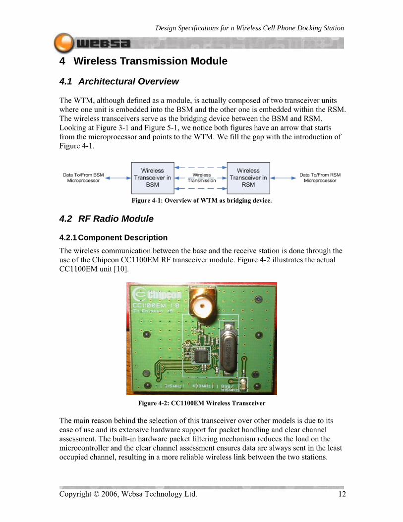
4.2 RF Radio Module 4.2.1 Component Description The wireless communication between the base and the receive station is done through the use of the Chipcon CC1100EM RF transceiver module. Figure 4-2 illustrates the actual CC1100EM unit [10].
Figure 4-2: CC1100EM Wireless Transceiver
The main reason behind the selection of this transceiver over other models is due to its ease of use and its extensive hardware support for packet handling and clear channel assessment. The built-in hardware packet filtering mechanism reduces the load on the microcontroller and the clear channel assessment ensures data are always sent in the least occupied channel, resulting in a more reliable wireless link between the two stations.

Design Specifications for a Wireless Cell Phone Docking Station
The transceiver is designed to operate within the ISM (Industrial, Scientific and Medical) and SRD (Short Range Device) frequency bands at 868 and 915 MHz [11]. In this application, we decided to choose 915 MHz as the operating frequency because this frequency lies within the 906-928MHz band, which is a legal frequency band in North America [11]. In contrast, the 868MHz band is only legal in Europe thus it cannot be used in North America. Another reason we chose this radio module is due to its high data rate. In our application, voice is sampled at 8 KHz (because human voice is roughly 4kHz and applying Nyquist’s sampling theorem, we result in a sampling frequency of 8kHz [12]) as an 8 bit sample. The PICF16877A provides a 10 bit ADC conversion resolution but only the most 8 significant bits are used for transmission only [13]. This requirement means the radio must be able to transmit at a minimum rate of 64kbps without taking the additional overhead frames before and after the voice data. The CC1100EM provides a user programmable data rate up to 250kbps, which allows for plenty of overhead to include other useful status frames to be sent along with the voice data. 4.2.2 Component Implementation The Chipcon CC1100 radio module uses Serial Peripheral Interface (SPI) as its main communication channel with the PIC16F877A microcontroller. SPI is a serial bus standard established by Motorola. The SPI employs a master / slave relationship, which utilizes four signals: clock (SCLK); master output, slave input (MOSI); master input, slave output (MISO); and slave select (SS).
Figure 4-3: Block diagram to illustrate connection between radio and MCU
Figure 4-3 shows a block diagram between the microcontroller and the radio module with the four SPI signals. The microcontroller acts as a master device which will supply the radio (slave) with a clock signal through SCLK. When the radio is selected by the microcontroller thru the slave select (SS) signal, data are transmitted in both directions simultaneously through the MOSI and MISO line. During a SPI transmission, data are always transferred in both directions between the master and the slave. It is the hardware’s responsibility to determine if the data is useful or not. For the SPI interface on the CC1100, all transaction starts with an 8 bit header byte containing a read / write bit, a burst access bit and a 6 bit address. When a header byte is sent on the SPI interface thru the MOSI line, a chip status byte will be sent back to the microcontroller thru the MISO signal path. The chip status byte contains key status signals useful for the microcontroller. Figure 4-4 illustrates registers read and write operation for the CC1100 radio [14].
Copyright © 2006, Websa Technology Ltd. 13
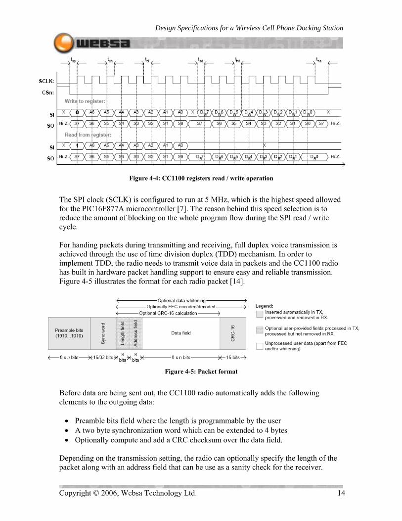
Design Specifications for a Wireless Cell Phone Docking Station
Figure 4-4: CC1100 registers read / write operation
The SPI clock (SCLK) is configured to run at 5 MHz, which is the highest speed allowed for the PIC16F877A microcontroller [7]. The reason behind this speed selection is to reduce the amount of blocking on the whole program flow during the SPI read / write cycle. For handing packets during transmitting and receiving, full duplex voice transmission is achieved through the use of time division duplex (TDD) mechanism. In order to implement TDD, the radio needs to transmit voice data in packets and the CC1100 radio has built in hardware packet handling support to ensure easy and reliable transmission. Figure 4-5 illustrates the format for each radio packet [14].
Figure 4-5: Packet format
Before data are being sent out, the CC1100 radio automatically adds the following elements to the outgoing data: • Preamble bits field where the length is programmable by the user • A two byte synchronization word which can be extended to 4 bytes • Optionally compute and add a CRC checksum over the data field.
Depending on the transmission setting, the radio can optionally specify the length of the packet along with an address field that can be use as a sanity check for the receiver.
Copyright © 2006, Websa Technology Ltd. 14

Design Specifications for a Wireless Cell Phone Docking Station
Copyright © 2006, Websa Technology Ltd. 15
5 Receiver Station Module 5.1 Architectural Overview The receiver station module (RSM) shown in Figure 5-1 provides an overview of the design that will meet the functional requirements set out in Websa Technology’s Functional Specification [3]. Six individual components make up the RSM, including the microcontroller unit (MCU), the Dual-Tone Multi-Frequency (DTMF) transceiver, the Digital to Analog Converter, the Data Access Arrangement (DAA), the call progress generator, and the ringer voltage generator. Each component is controlled by a single PIC16F877A MCU. The MCU is also connected to (and controls) the part of the WTM that resides in the RSM.
Figure 5-1: Architectural Overview of Receiver Station Module
When a corded or cordless handset is lifted off hook for the purpose of dialing an outgoing call, a dial tone is expected to signal the readiness of the unit. This dial tone can be achieved by the use of a call progress generator (CPG). In addition, the CPG is also capable of generating alert tones, which is used to signal a handset is off hook and no input has been received for a predetermined timeout period. Since the RSM must be able to transmit and receive audio and touch tone signals, the DAA provides the necessary telephone line interface between analog transmission equipment (the DTMF transceiver) and the TIP and RING lines. Digital voice signals that are received by the MCU from the WTM must be converted into analog signals before they can be understood by the DAA. The DTMF transceiver is used to decode and generate touch-tone audio signals, which are to be heard by the user when the keys on a handset are pressed. Because any corded or cordless handset that is connected to the RSM must ring upon detection of an incoming call, a ringer voltage generator circuit is required. The following sub sections detail the specifications of each component and its implementation.

Design Specifications for a Wireless Cell Phone Docking Station
5.2 Microcontroller Unit The MCU (Microchip’s PIC16F877A), with its component description already presented in section 3.3, will be the single source of control for the RSM. Its implementation is similar to that of the BSM, with the I/O pins assigned for controlling the DTMF, DAA, DAC, CGP and the ring voltage generator circuit. 5.3 DTMF Transceiver 5.3.1 Component Description The MT8880CE, shown in Figure 5-2, is a fully integrated DTMF transceiver used within the receiver station module (RSM) and is manufactured by Zarlink Semiconductor [15].
Figure 5-2: MT8880CE Pin Connections.
Table 5-1: Functional Encode/Decode ( 0 = Logic Low, 1 = Logic High)
FLOW FHIGH Digit D3 D2 D1 D0 697 1209 1 0 0 0 1 697 1336 2 0 0 1 0 697 1477 3 0 0 1 1 770 1209 4 0 1 0 0 770 1336 5 0 1 0 1 770 1477 6 0 1 1 0 852 1209 7 0 1 1 1 852 1336 8 1 0 0 0 852 1477 9 1 0 0 1 941 1336 0 1 0 1 0 941 1209 * 1 0 1 1 941 1477 # 1 1 0 0 697 1633 A 1 1 0 1 770 1633 B 1 1 1 0 852 1633 C 1 1 1 1 941 1633 D 0 0 0 0
Copyright © 2006, Websa Technology Ltd. 16

Design Specifications for a Wireless Cell Phone Docking Station
The MT8880CE communicates through the microprocessor over a 4-bit bus (D3 to D0). It contains an internal counter that provides a burst mode so that the tone burst can be transmitted with precise timing. The chip is capable of generating all 16 pairs of DTMF signals by utilizing a switched-capacitor D/A converter for low distortion and high accuracy DTMF signaling. In addition, the MT8880CE is capable of analyzing call progress tones with it’s built in call progress filter. Table 5-1 (above [15]) outlines all the 4-bit bus values with the corresponding digit values and dual frequencies. A list of pin assignments and the description for the 20-pin MT8880CE (shown in Figure 5-2) is provided in Table 5-2 [15].
Table 5-2: MT8880CE Pin Descriptions.
Finally, the attractiveness of the Zarlink MT8880CE DTMF chip is due to its dual in-line packaging and a maximum dimension of 26.92mm x 7.11mm x 5.33mm. Both its packaging and compact size make this a suitable selection for our RSM.
Copyright © 2006, Websa Technology Ltd. 17

Design Specifications for a Wireless Cell Phone Docking Station
5.3.2 Component Implementation The MT8880CE can be connected to the MCU as per the implementation illustration shown in Figure 5-3 [15].
Figure 5-3: MT8880CE Single Ended Input Configuration (μP = Microprocessor, i.e. MCU).
The single-ended input will be the implementation method used with the MT8880CE. Provisions for gain adjustments are made by connecting a feedback resistor between the Gain Select pin, GS, and the Inverting Input pin, IN-. A check on the validation of the signal duration, with the use of a steering circuit, is required before registration of a decoded tone pair in the internal register can be made. The steering circuit involves the use of an external RC circuit with a time constant driven by the Steering Input pin, ESt. The dual tone signals are generated by an internal clock, which requires a standard burst crystal with a resonant frequency of 3.579545MHz. The typical operating supply voltage for the configuration in Figure 5-3 is 5V and is supplied into the VDD pin. The suggested capacitor and the resistor values provided by the data sheet ([15]) will be followed closely to obtain the best results while preventing any damages to the DTMF chip or any other electronic components. 5.4 Digital to Analog Converter The DAC used in the RSM will be implemented the same way as it is in the BSM. Its detailed component description and implementation was presented in section 3.4. The input to the DAC will come from the MCU and its output (an analog voltage signal) will
Copyright © 2006, Websa Technology Ltd. 18

Design Specifications for a Wireless Cell Phone Docking Station
be connected to the DAA before reaching the telephone handset through the TIP and RING wires. 5.5 Telephone Line Interface 5.5.1 Component Description The MITEL MH88435AD DAA chip is used for the telephone line interface. Under DTMF operation, the MH88435AD provides a complete interface between audio or data transmission and a telephone line. This chip was chosen due to its low cost and ease of implementation. In addition, this DAA is able to provide isolation and surge protection (for the other electronic components) from the telephone line Figure 5-4 and Figure 5-5 illustrates the pin connection and functional block diagram, respectively [16].
Figure 5-4: MH88435AD Pin Configuration.
Figure 5-5: MH88435AD Functional Block Diagram.
Copyright © 2006, Websa Technology Ltd. 19

Design Specifications for a Wireless Cell Phone Docking Station
The features of the MH88435AD include high voltage isolation barrier, 2-to-4 wire conversion, externally programmable line, and network balance impedances. Furthermore, this DAA is capable of variable ring voltage sensitivity. To understand the function of the MH88435AD further, its pin descriptions are presented in the table below [16].
Table 5-3: MH88435 Pin Descriptions.
Copyright © 2006, Websa Technology Ltd. 20

Design Specifications for a Wireless Cell Phone Docking Station
5.5.2 Component Implementation Figure 5-6 illustrates a typical application circuit for the MH88435AD DAA chip [16]. Instead of placing a dummy ringer load across the TIP and RING wires as suggested in the data sheet, however, we’ve attached a working ringer voltage generator.
Figure 5-6: MH88435AD Application Circuit.
The MH88435AD’s analog output shown in the figure above will be connected to the input of the MT8880CE configuration shown in Figure 5-3. The differential analog input in Figure 5-6 will be supplied by voice signals (during a call) and call progress tones (while dialing). The TIP and RING wires, shown in Figure 5-6, correspond to the two-wire telephone connection and will be connected to a standard RJ11 telephone jack. Aside from the slight modification stated above, we will follow this circuit configuration closely to prevent damage to the DAA chip or other electronic components.
Copyright © 2006, Websa Technology Ltd. 21
Design Specifications for a Wireless Cell Phone Docking Station
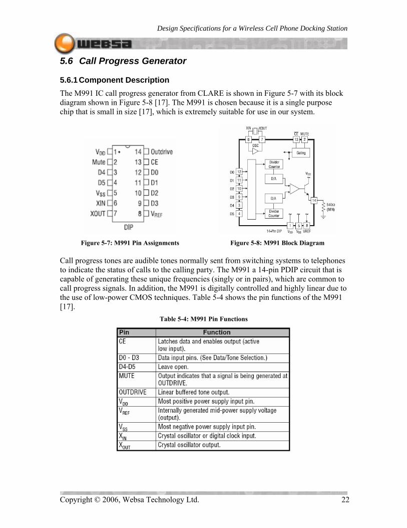
5.6 Call Progress Generator 5.6.1 Component Description The M991 IC call progress generator from CLARE is shown in Figure 5-7 with its block diagram shown in Figure 5-8 [17]. The M991 is chosen because it is a single purpose chip that is small in size [17], which is extremely suitable for use in our system.
Figure 5-7: M991 Pin Assignments Figure 5-8: M991 Block Diagram
Call progress tones are audible tones normally sent from switching systems to telephones to indicate the status of calls to the calling party. The M991 a 14-pin PDIP circuit that is capable of generating these unique frequencies (singly or in pairs), which are common to call progress signals. In addition, the M991 is digitally controlled and highly linear due to the use of low-power CMOS techniques. Table 5-4 shows the pin functions of the M991 [17].
Table 5-4: M991 Pin Functions
Copyright © 2006, Websa Technology Ltd. 22

Design Specifications for a Wireless Cell Phone Docking Station
Table 5-5 shows the commonly used call progress tones and the proper bit values for duration and frequency selections of that particular tone [17]. A reference table for standard call progress tones is shown in Table 5-6, which allows us to compare the actual behavior of the chip to this chart for verification purposes [17].
Table 5-5: M991 Data/Tone Selection
Table 5-6: Standard Call Progress Tones.
5.6.2 Component Implementation Referring to Figure 5-8, the MCU will be connected to the call progress generator via pins D0 to D3 to trigger the generation of the desired tones. Pins D4 and D5 must be left open, however. The output of the M991 will be connected to the input of the DTMF chip (Figure 5-3). This chip will be powered by +5V DC.
Copyright © 2006, Websa Technology Ltd. 23

Design Specifications for a Wireless Cell Phone Docking Station
5.7 Ring Voltage Generator 5.7.1 Component Description The ring voltage generator is a low cost switching supply circuit designed using common electronic components that is responsible for producing the necessary high voltage to trigger the ringer in a normal telephone. This voltage is usually between 40 and 150 Volts DC at a frequency of 20 – 40Hz [18]. We have designed our circuit to produce 75V DC at the output at 30Hz when it is connected (i.e. when there is an incoming call). Figure 5-9 shows the circuit schematic (adopted from Bill Bowden’s design [19]), with value modified from the original drawing to yield different ringer interval values and input voltage.
Figure 5-9: Circuit diagram for ringer voltage generator using switching supply.
5.7.2 Component Implementation
The circuit will be activated by the MCU. The MCU output pins are capable of generating 5V [7]. Since we require 5.5V, as shown in the above figure, an operation amplifier (LM324) will be used to amplify the voltage. The outputs shown in the above figure will be connected directly to the TIP and RING wires shown in Figure 5-6.
Copyright © 2006, Websa Technology Ltd. 24

Design Specifications for a Wireless Cell Phone Docking Station
Copyright © 2006, Websa Technology Ltd. 25
6 System Event Flow The subsections below detail the various high level system event flows of each module and the event interactions between the modules. These designs will help with the low level assembly programming that will commence shortly after this design specification is completed. The flow diagrams will also provide the testing procedures when the microprocessor programming is complete. 6.1 Base Station Module 6.1.1 Idle State A cell phone status flag is kept inside the MCU to monitor the existence of the mobile phone. When the system is first powered, the BSM assumes that no cell phone is plugged in and the BSM state is set to NO_MOBILE_PHONE. The microcontroller then tries to send a command to the mobile phone to request its power status. If the cell phone replies with an OK status bit, it means that there is a cell phone connected to the BSM and it is powered on. Upon receiving the positive acknowledgement from the cell phone, the BSM enters into the IDLE state. The IDLE state denotes that a cell phone has been connected and the BSM is awaiting the next instruction. 6.1.2 Incoming Call Connection This scenario shows the procedures of receiving and answering incoming cell phone calls. The successful establishment of a communication channel between mobile phone and home phone depends on the status of the RSM and the WTM. It requires both modules to be in IDLE state ready for receiving commands. Data exchange between the MCU and the cell phone is done by the built-in Universal Synchronous Asynchronous Receiver Transmitter (USART). The baud rate of the USART is set to 9600 Hz to agree with the GSM modem clock rate inside the mobile phone. Data is transmitted in unit of packets. Each packet has 10 bits with the first and last bit serving as the starting bit and stopping bit, respectively. The middle 8 bits are the information bits. Whenever the MCU has finished receiving one packet, an interrupt flag bit is set by the hardware, which causes the interrupt routine to run. Inside the interrupt routine, the received packet is compared with pre-defined masks and the associated interrupt handler is called. When the mobile phone receives an incoming call request, its GSM modem will send a RING notification to the BSM. At this stage, the mobile phone is assumed to be connected with the MCU and the BSM is in its IDLE state. Upon receiving the RING indication, the BSM switches from IDLE state to INCOMING_CALL state. A packet is also sent to the RSM indicating an incoming call request along with the BSM state. The RSM is expected to return the proper acknowledgment (on-hook or off-hook). If the reply from the RSM shows that the landline phone is off-hook (i.e. the handset has been picked up before the incoming call), the BSM will continue to send the incoming call request to

Design Specifications for a Wireless Cell Phone Docking Station
the RSM until the caller stops calling or until the user places the handset back to the on-hook position. If the RSM returns with the acknowledgement that the home phone is on-hook, then the RSM is ready to receive calls. If the first acknowledgement indicates that the landline communication device is on-hook, the BSM changes the state from INCOMING_CALL to AWAITING_ANSWER state. When the RSM replies again after another state inquiry which indicates the telephone is still on-hook, the BSM, in the AWAITING_ANSWER state, will send an AT command to the cell phone to indicate that the Docking Station is ready for voice communication. The ADC is now turned on and the voice communication channel is now created. Both BSM and RSM then enter the ACTIVE state (the state where a communication is established). If the caller disconnects the call before the user picks up, a TERMINATE packet is sent to the MCU via the USART. Upon receiving this indication, the BSM will forward this message to the RSM and change its own state from AWAITING_ANSWER to IDLE.
Figure 6-1: Flow Chart of Incoming Call Algorithm
6.1.3 Outgoing Call Connection The outgoing call procedures are similar to that of the incoming call except the direction is reversed. Whenever there is a data packet from the RSM, the DATA_READY flag is set by the WTM. The BSM periodically monitors this flag to catch any data that is available. Pre-defined bit-map masks are adopted to compare the different statuses. If an outgoing call request is received, the BSM immediately answers with a packet indicating the connection status of the mobile phone given that the BSM is in IDLE state. The BSM then waits for the dialing strings (DS) from the RSM. The DS is a string of numbers that the user inputs to make an outgoing call (i.e. 6042914400).
Copyright © 2006, Websa Technology Ltd. 26

Design Specifications for a Wireless Cell Phone Docking Station
The BSM state is not changed until the DS is provided by the RSM. A packet indicating the starting of string transfer is expected by the BSM. The packets that follow are treated as strings and forwarded to the mobile device until the ending of string transfer packet is obtained. The ADC is then turned on and the BSM is changed into the DIALING state. If the call is accepted by the intended recipient, a CONNECT packet is transmitted from the cell phone GSM modem to the MCU. The BSM is then switched from DIALING to ACTIVE state. The ACTIVE state indicates that a conversation is currently in progress.
Figure 6-2: Flow Chart of Outgoing Call Algorithm
6.1.4 Voice Communication The PICF16877A microcontroller’s pin 2 (bit 0 of PORT A) is reserved as an analog input pin. During communication, voice signals are extracted from the voice output pin of the mobile phone and fed into pin 2 of the MCU. The built in ADC is sampling the analog signal at a specified conversion rate (mentioned in section 4.2.1). The voice data from the RSM is stored in the SPI receive buffer and its contents are also updated every 1/8K sec. Voice data is written to PORT D of the MCU and then converted back to analog signal with the aid of external digital-to-analog converter. The output of the DAC is connected with the voice input of the mobile phone. The communication cycle repeats continuously until a TERMINATE packet is received from either the RSM or the mobile phone. If the packet is sent from the cell phone, BSM will forward the message to the RSM and switches back to IDLE mode. On the other hand, if the packet sent is from the RSM, an AT command is issued to the mobile device to terminate the voice channel and the BSM is set to the IDLE state again. Table 9-1 to Table 9-4 in the Appendix describes in detail the binary bit values assigned for the states and flags mentioned above.
Copyright © 2006, Websa Technology Ltd. 27

Design Specifications for a Wireless Cell Phone Docking Station
6.2 Wireless Transmission Module 6.2.1 Time Division Multiplexing The objective of time division duplex (TDD) is to utilize the half duplex wireless link in a way that will appear to the user as a full duplex link. The half duplex link, which can only transmit or receive at a given time, must switch between transmit and receive mode fast enough and often enough to appear to the user as a full duplex link. The figure below shows the timing in which the base and receiver RF modules switches between transmit and receive modes to achieve TDD. As shown, the wireless link switches between the two states – transmitting from base to receiver station and transmitting from receiver to base station. A short period of guard time is also added in between the two states when wireless transmission is in opposite directions. This guard time is represented by the overlap when both base and receiver stations are in receive mode. It has been tested and verified that safe operation is possible when both wireless units are in receive mode. However, it has not been tested when both wireless units are in transmit mode. However, we can intelligently conclude that if both units are transmitting, there will be packet loss because no transmitted packets are being received. In addition, jamming may occur if both units are transmitting at the same time without any receivers.
Figure 6-3: Base and receiver TDD receive and transmit mode switching scheme. Horizontal axis
represents the time axis.
Another form of illustration would help understand the concept of TDD further. The figure below shows the TDD event flow during a voice call, with the voice packet payload being 10 ms of voice data for example purposes. The base station and receiver station alternates in sending voice data back and forth, switching the send direction every 5 ms or half a packetization time. We start off the example with the base station being the transmitting side. The restriction is that the time to transmit the voice packet must be less than half the packetization time (or 5 ms in this case). The transmitting side (base station) will then switch to receive mode after packet transmission is complete, forming the guard time as indicated by the green shaded portions in the diagram below. The receiving side (receiver station) will receive the voice data into a buffer during the guard time, and then switch to transmit mode after it accumulates 10 ms of voice data, ending the guard time. Now, the wireless link transmit direction has switched fully, from base sending to receiver station to receiver sending to base station. This cycle of voice alternation wireless link transmit direction continues as long as there is a call in progress.
Copyright © 2006, Websa Technology Ltd. 28

Design Specifications for a Wireless Cell Phone Docking Station
Figure 6-4: Base and receiver TDD event flow during a voice call. Vertical axis represents the time
axis. Voice packet payload is 10ms of voice data in this case for example purposes.
6.2.2 Program Flow Figure 6-5 is the program flow chart of the wireless module. Upon power up of the system, the RF module settings and SPI interface settings are initialized along with other miscellaneous initialization steps. The wireless module will first check to see if 10 ms of voice data has been accumulated yet. Once the 10 ms voice data packet payload has been accumulated, the wireless module performs the tasks as represented by the “Dump voice into RF module” block in Figure 6-4. The tasks include setting the RF modules to transmit mode, dumping the packet payload into the RF module via SPI interface, and clearing the data buffer in the MCU. All these are done with interrupts disabled to ensure the packet payload transfer does not get interrupted. Whether a voice packet or an instruction packet is transmitted depends which payload type is available, but instruction payload type has higher priority than voice payload type. If both payload types are available, instruction payload will be transmitted and the voice payload will be ignored. Now that the packet is transmitted, the wireless module will check to see when the packet transmission is finished, or in other words checking when the TX FIFO of the RF module is empty. When packet transmission is finished, the RF module is switched to receive mode, again with the interrupts disabled. This initiates the beginning of the guard time until the other side of the wireless link switches to transmit mode. Next, the wireless module will check when the RF module has received the packet. When the packet is received, the payload data will be dumped to the MCU buffer via SPI interface, again with the interrupts disabled. After receiving from the other side of the
Copyright © 2006, Websa Technology Ltd. 29

Design Specifications for a Wireless Cell Phone Docking Station
wireless link, the wireless module is now ready to loop back to beginning of the flow chart and check for when it should transmit another packet.
Figure 6-5: Flow chart of the wireless module program flow.
Copyright © 2006, Websa Technology Ltd. 30

Design Specifications for a Wireless Cell Phone Docking Station
6.3 Receiver Station Module 6.3.1 Incoming Call Event Flow The incoming call event flow is illustrated in Figure 6-6. Assuming the home phone is on- hook, the RSM will be in IDLE state and will continuously monitor for incoming calls. When a call arrives, the ringer will be turned on and the microprocessor awaits the user to pick up the telephone. When the handset is lifted, the ringer shuts off and the RSM enters the TALKING state, allowing the user to engage in a normal conversation. Two factors will cause the RSM to return to the IDLE state; if the user hangs up and places the handset on-hook or if the cell phone disconnects either through lost of reception or if the opposing party hangs up.
Figure 6-6: RSM incoming call event flow.
6.3.2 Outgoing Call Event Flow The outgoing call event flow is illustrated in Figure 6-7. This event occurs if a user wishes to dial an outgoing call. The phone first needs to be on-hook to ensure it is in the IDLE state. When an off-hook is detected and there are no incoming calls at the same time, the dial tone will be generated for the user. A dial_tone_timeout counter is automatically started. Once this timer reaches 0, the dial tone switches over to an off-hook warning tone. This is analogous to if a user accidentally knocks off their telephone accidentally. Before the dial_tone_timeout is reached, if a key is pressed, the telephone switches to normal operation and continually accepts the key presses, generating the corresponding DTMF tones for the user.
Copyright © 2006, Websa Technology Ltd. 31
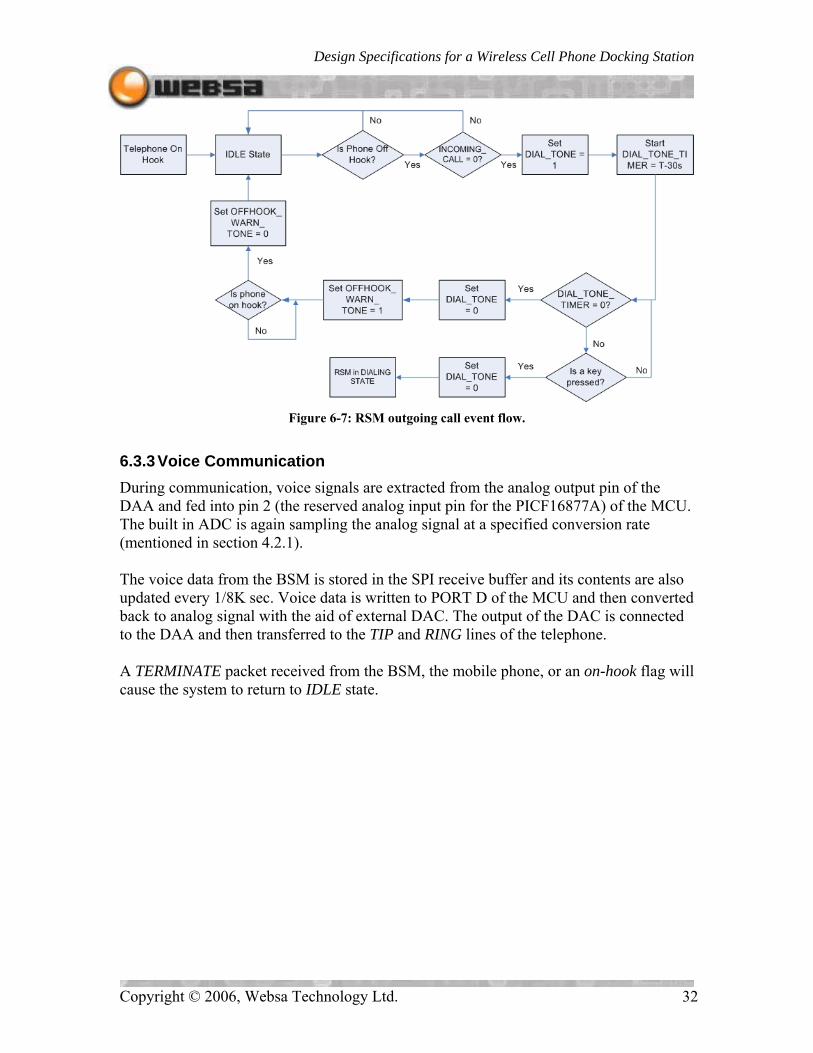
Design Specifications for a Wireless Cell Phone Docking Station
Figure 6-7: RSM outgoing call event flow.
6.3.3 Voice Communication During communication, voice signals are extracted from the analog output pin of the DAA and fed into pin 2 (the reserved analog input pin for the PICF16877A) of the MCU. The built in ADC is again sampling the analog signal at a specified conversion rate (mentioned in section 4.2.1). The voice data from the BSM is stored in the SPI receive buffer and its contents are also updated every 1/8K sec. Voice data is written to PORT D of the MCU and then converted back to analog signal with the aid of external DAC. The output of the DAC is connected to the DAA and then transferred to the TIP and RING lines of the telephone. A TERMINATE packet received from the BSM, the mobile phone, or an on-hook flag will cause the system to return to IDLE state.
Copyright © 2006, Websa Technology Ltd. 32

Design Specifications for a Wireless Cell Phone Docking Station
Copyright © 2006, Websa Technology Ltd. 33
7 Conclusion This design specification of Websa Technology’s Wireless Cell Phone Docking Station provides an idea of how our developing team hopes to implement and construct each module: Base Station Module, Wireless Transmission Unit, and Receiver Station Module. This document also outlined the architectural layout, selected components, and implementation procedures to provide a more comprehensive insight of the low-level design. All designs were carefully thought out and specifically chosen to meet the requirements set by the Functional Specifications. Upon completion of this project in April 2006, our developing team is confident that our prototype, the Wireless Mobile-Dock, will satisfy the minimum functional requirements using the designs presented in this document.
Design Specifications for a Wireless Cell Phone Docking Station
Copyright © 2006, Websa Technology Ltd. 34
8 References [1] CTIA The Wireless Association Oct. 2005. Wireless Quick Facts. 02 Mar. 2006
<http://files.ctia.org/pdf/Wireless_Quick_Facts_October_05.pdf> [2] U.S. Census Bureau 26 April 2005. World POPClock Projection. 02 Mar. 2006
<http://www.census.gov/ipc/www/popclockworld.html> [3] Websa Technology 2006. Functional Specifications for a Wireless Cell Phone
Docking Station. Simon Fraser University, Burnaby, BC, Canada, February 2006. [4] MobilePhonesUK 2006. Sony Ericsson T310 Review. 1 March 2006
<http://www.mobile-phones-uk.org.uk/images/sonyericssont310.gif> [5] Get Wired.com 2005. SonyEricsson T310 cell phone pinout. 16 Feb. 2006
<http://pinouts.ru/data/erics_t28_pinout.shtml>
[6] SonyEricsson.com 2006. AT Commands Online Reference. 25 Jan. 2006 <http://developer.sonyericsson.com/getDocument.do?docId=65054>
[7] Microchip.com 2006. PIC16F877A DataSheet. 9 Feb. 2006
<http://ww1.microchip.com/downloads/en/DeviceDoc/39582b.pdf> [8] Analog.com 2006. Analog Devices AD7533. 24 Feb. 2006
<http://www.analog.com/UploadedFiles/Data_Sheets/124713472AD7533_b.pdf> [9] National.com 2006. LM324 Product Folder. 25 Feb. 2006
<http://www.national.com/ds.cgi/LM/LM124.pdf> [10] HobbyWiki 2006. CC1100 Transceiver 03 Mar. 2006
<http://wiki.hobbyist.de/index.cgi?CC1100> [11] ITU 2006. International Telecom Union. 06 Mar. 2006
<http://www.itu.int/home/index.html?> [12] Wikipedia 2006. Nyquist frequency. 06 Mar. 2006
<http://en.wikipedia.org/wiki/Nyquist_frequency> [13] Microwaves and RF 2006. Low-Power Transceivers Target Wireless Handsets. 03
Mar. 2006 <http://www.mwrf.com/Articles/Print.cfm?ArticleID=5525> [14] Chipcon 2006. CC1100 Single Chip Low Cost Low Power RF Transceiver. 07 Mar.
2006 <http://www.chipcon.com/files/CC1100_data_sheet_1_0.pdf> [15] Zarlink Semiconductor Sept 2005. Integrated DTMF Transceiver. 04 Mar. 2006
<http://assets.zarlink.com/DS/zarlink_MT8880C_SEP_05.pdf>

Design Specifications for a Wireless Cell Phone Docking Station
Copyright © 2006, Websa Technology Ltd. 35
[16] MITEL Semiconductor 2006. Data Access Arrangement. 04 Mar. 2006 <http://www.gaw.ru/doc/Mitel/MH88435.PDF>
[17] CLARE 2006. Call Progress Generator. 04 Mar. 2006
<http://www.clare.com/home/pdfs.nsf/www/M991.pdf/$file/M991.pdf> [18] Phone Warehouse 20 Feb. 2002. Telephone Ringer Fact and Telephone Descriptions.
06 Mar. 2006 <http://www.affordablephones.net/Theringer.htm>. [19] Bowden’s Hobby Circuits 15 Jan. 1999. Telephone Ring Generator Using Switching
Supply. 03 Mar. 2006 <http://ourworld.compuserve.com/homepages/Bill_Bowden/ page11.htm#ring2.gif>

Design Specifications for a Wireless Cell Phone Docking Station
Copyright © 2006, Websa Technology Ltd. 36
9 Appendix
Table 9-1: Base Station Module Data Packet Format
7 6 5-3 2-0 MIB -- CS BSMS
Table 9-2: Bit Representation of Status and States
MIB: Module Indication Bit
CS: Cell-Phone Status BSMS: Base Station Module State
0: Cell Phone Module 0: OK 000: NO_MOBILE_PHONE 1: Landline Phone Module 1: CONNECT 001: IDLE 2: RING 010: INCOMMING_CALL 3: NO CARRIER 011: WAITING_ANSWER 4: ERROR 100: DIALING 5: NO DIALTONE 101: ACTIVE 6: BUSY 7: NO ANSWER
Table 9-3: 8-bits Binary Representation of Cell Phone Status
Cell Phone Status Binary Mask OK 00000000 11111111 CONNECT 00000001 11111110 RING 00000010 11111101 NO CARRIER 00000011 11111100 ERROR 00000100 11111011 NO DAILTONE 00000101 11111010 BUSY 00000110 11111001 NO ANSWER 00000111 11111000
Table 9-4: 8-bits Binary Representation of Base Station Module State
BSM State Binary Mask NO_MOBILE_PHONE 00000001 11111110 IDLE 00000010 11111101 INCOMMING_CALL 00000100 11111011 DIALING 00001000 11110111 WAITING_ANSWER 00010000 11101111 ACTIVE 00100000 11011111