Embed Size (px)
Citation preview

External Use
TM
Design to Tight
Power Supply Requirements
FTF-NET-F0036
A P R . 2 0 1 4
Chuck Corley | DMTS
Mohit Kedia | Engineering Rotation Program

TM
External Use 1
Abstract: Design to Tight Power Supply Requirements
• Session Length: 2 hours
• Freescale has begun specifying core supply voltages with ±30 mV
tolerances. Customers are accustomed to ±5% and are asking
questions about how to achieve this tighter requirement. This
presentation will discuss the specification and what customers need
to know for successful designs.

TM
External Use 2
Agenda
• Defining the problem
−3% DC voltage requirement
−Time versus frequency domain
• VDD/PLAT Voltage Specification for T
(28nm) series parts
• Current step observations for T4240RDS
• Current step observations for T1040QDS
• Discussion of current slew rate

TM
External Use 3
Defining the Problem
Requirements
• Power Supply must supply a stable voltage reference
• Power Supply must distribute adequate current
Observations:
• Switching power supplies actually supply a digitally varying voltage (~500 KHz)
• Microprocessor’s current demand may vary as fast as core frequency (~2GHz)
• Power Distribution Network (PDN) has resistance, capacitance, inductance, mutual capacitance, and mutual inductance through PCB, socket, vias, and capacitors.
• Changes in current at a particular frequency causes voltage changes at that frequency across these impedances.
Problem:
• Silicon vendors are tightening the voltage specifications while the current continues to increase.
TM
External Use 4
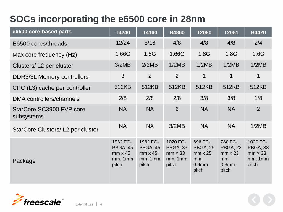
SOCs incorporating the e6500 core in 28nm
e6500 core-based parts T4240 T4160 B4860 T2080 T2081 B4420
E6500 cores/threads 12/24 8/16 4/8 4/8 4/8 2/4
Max core frequency (Hz) 1.66G 1.8G 1.66G 1.8G 1.8G 1.6G
Clusters/ L2 per cluster 3/2MB 2/2MB 1/2MB 1/2MB 1/2MB 1/2MB
DDR3/3L Memory controllers 3 2 2 1 1 1
CPC (L3) cache per controller 512KB 512KB 512KB 512KB 512KB 512KB
DMA controllers/channels 2/8 2/8 2/8 3/8 3/8 1/8
StarCore SC3900 FVP core
subsystems
NA NA 6 NA NA 2
StarCore Clusters/ L2 per cluster NA NA
3/2MB NA NA 1/2MB
Package
1932 FC-
PBGA, 45
mm x 45
mm, 1mm
pitch
1932 FC-
PBGA, 45
mm x 45
mm, 1mm
pitch
1020 FC-
PBGA, 33
mm × 33
mm, 1mm
pitch
896 FC-
PBGA, 25
mm x 25
mm,
0.8mm
pitch
780 FC-
PBGA, 23
mm x 23
mm,
0.8mm
pitch
1020 FC-
PBGA, 33
mm × 33
mm, 1mm
pitch

TM
External Use 5
Tight Core Voltage Specifications for 28nm
e6500 core-based parts T4240 T4160 B4860 T2080/81 B4420
Core and platform supply Voltage - startup 1.05 V ± 30
mV
1.05 ± 30
mV
1.05 V ± 30
mV
1.025 ± 30
mV
1.05 V ± 30
mV
Core and platform supply Voltage – normal
operation
VID ± 30
mV
VID ± 30
mV
VID ± 30
mV
VID ± 30
mV
VID ± 30
mV
Operation at 1.1V is allowable for up to 25ms at
initial power on.
footnote 6 footnote 6 footnote 6 footnote 3 footnote 5
Voltage ID (VID) operating range is between
0.95V to 1.05V. Regulator selection should be
based on Vout range of at least 0.9V to 1.1V, with
resolution of 12.5mV or better.
0.9V but
changing
to 0.95
0.9V but
changing
to 0.95
footnote 1 footnote 7
0.975-
1.025
0.9V
…maintain the transient power surges to less
than +50 mV (negative transient undershoot
should comply with specification of VID-30mV) for
current steps of up to 20 A for 12 cores, 15A for 8
cores and 10A for 4 cores with a slew rate of 12
A/us.
Section
4.2.2
Section
4.2.2
S3.2.2:
± 30 mV;
no step
spec’d
Section
4.2.2
10A step
Footnote 4;
S3.2.2:
+50/-30
mV 1-
200MHz;
+100mV
transient;
20A step
it is recommended that the system designer place
at least one (0.1μF) decoupling capacitor at each
VDD, VDDC, CVDD, OnVDD, DVDD, EVDD,
GnVDD, and LnVDD pin of the device.
Section 4.3 Section 4.3 Section 3.3
Section 4.3 Section 3.3
Spec Rev Rev G Rev D Rev H Rev E/D Rev C
TM
External Use 6
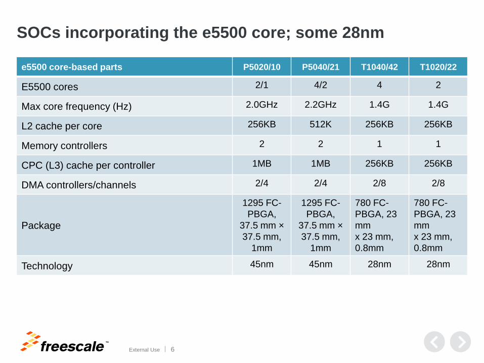
SOCs incorporating the e5500 core; some 28nm
e5500 core-based parts P5020/10 P5040/21 T1040/42 T1020/22
E5500 cores 2/1 4/2 4 2
Max core frequency (Hz) 2.0GHz 2.2GHz 1.4G 1.4G
L2 cache per core 256KB 512K 256KB 256KB
Memory controllers 2 2 1 1
CPC (L3) cache per controller 1MB 1MB 256KB 256KB
DMA controllers/channels 2/4 2/4 2/8 2/8
Package
1295 FC-
PBGA,
37.5 mm ×
37.5 mm,
1mm
1295 FC-
PBGA,
37.5 mm ×
37.5 mm,
1mm
780 FC-
PBGA, 23
mm
x 23 mm,
0.8mm
780 FC-
PBGA, 23
mm
x 23 mm,
0.8mm
Technology 45nm 45nm 28nm 28nm

TM
External Use 7
Tight Core Voltage Specifications for e5500 & 28nm
e5500 core-based parts P5020/10 P5040/21 T1040/42/20/22
Core and platform supply Voltage - startup 1.0 ±
50mV(core
frequency =
1200 MHz)
1.1V ± 50mV
(core
frequency >
1200 MHz)
1.1 ± 50mV
(core
frequency ≤
2000 MHz)
1.2V ± 30mV
(core
frequency >
2000 MHz)
1.025 ± 30 mV
Core and platform supply Voltage – normal operation
VID ± 30 mV
Operation at 1.1V is allowable for up to 25ms at initial power
on.
NA NA footnote 5
Voltage ID (VID) operating range is between 0.975V to
1.025V. Regulator selection should be based on Vout range of
at least 0.9V to 1.1V, with resolution of 12.5mV or better.
NA NA footnote 7
…maintain the transient power surges to less than +50 mV
(negative transient undershoot should comply with
specification of VID-30mV) for current steps of up to 20 A for
12 cores, 15A for 8 cores and 10A for 4 cores with a slew rate
of 12 A/us.
NA NA Section 4.2.2
10A step
…at least one (0.1μF) decoupling capacitor at each VDD,
VDDC, CVDD, OnVDD, DVDD, EVDD, GnVDD, and LnVDD
pin of the device.
Section 3.4
0.01 or 0.1μF*
Section 4.3
0.01 or 0.1μF*
Section 4.3
Spec Rev Rev 0 Rev 0 Rev E
Better to use largest capacitance that will fit on footprint under the part.

TM
External Use 8
What is Voltage ID (VID) for 28nm Products?
• A specific method of selecting the optimum voltage-level to
guarantee performance and power targets. − QorIQ device contains fuse block registers defining required voltage level. This EFUSE
definition is accessed through the Fuse Status Register (DCFG_FUSESR).
− Customer system must use the VID to change the voltage regulators in the system in a
reliable and safe methodology.
• QorIQ Chassis Architecture Specification, Generation 2 Revision 0.9
defines the general EFUSE definition.
− A set of 24 efuses ([0-23]) that determine the speed bin and voltage requirements for the
device domains.
− The range and steps are much more flexible than actually needed by manufacturing; only
the fuses necessary to provide the required voltages will be implemented.

TM
External Use 9
Voltage Specification Terms Better Defined
time
vDD
IDD
Step-up Step-down
Load-Step
Undershoot
OvershootVID or
DCSetPoint
Tolerance VID +50mV / -30mV
Switching
RipplePrincipal Silicon
Concern

TM
External Use 10
Power Distribution System Theory – VRMs
• Voltage Regulator Modules (VRMs) use feedback to hold a constant
supply voltage (up to the frequency of the inherent low pass filter).
• QorIQ parts allow feedback from the die voltage plane – SENSEVDD
• T4240QDS Intersil VRM (typical of most VRMs) advertises ±0.5%
Closed-loop System Accuracy Over Load, Line and Temperature [for
transients < 1/3 (to 1/5) of switching frequency – 350-500kHz].
Vref
+- LPF
Bulk
Caps Bypass
Caps
Planes
From Intel VRM 11.1

TM
External Use 11
VrefBulk
Caps
Bypass
Caps
Planes
DIE
SENSEVDD_P
-
VDD
~One
0.1uF
per
pin
SENSEVDD_N
PKG
+12V
ST
SB
LF
VRM Model PDN System
Mult
22 to
1000uF
caps
ESR
VID ± 30 mV

TM
External Use 12
Power Distribution System Theory - Ripple
• The most common meaning of ripple in electrical science is the small unwanted residual periodic variation of the direct current (dc) output of a power supply which has been derived from an alternating current (ac) source. This ripple is due to incomplete suppression of the alternating waveform within the power supply.
VRIPPLE – P-P at Bulk Capacitors
PWM current spikes from +12V supply when ST conducts
time
Voltage
TM
External Use 13
Power Distribution System Theory – AC Impedance
• Inductance in the traces and vias (and socket pogo pins) create an AC impedance (ZS) that causes dv/dt changes at the load with varying di/dt.
• These dv/dt changes would “ride” on any DC voltage droop.
• Decoupling capacitors and capacitive plane layers are added to reduce the AC impedance between VDD and GND.
+
-VL
IL
VS = 1.00 V
DC
ZS
Vref
+- LPF
Bulk
Caps
Bypass
Caps
Planes
DIE
SENSEVDD_P
-
VDD30ea
22uF
83ea
0.1uF
+-
SENSEVDD_N

TM
External Use 14
Reactive Elements in the PDN cause dv/dt
• Well documented problem (see references slide)
• Silicon vendors are tightening the DC specifications at lower
supply voltages.
• Customers are demanding more information from silicon
vendors to aid in designing compliant power supplies (Power
Distribution Networks or PDNs).

TM
External Use 15
The PDN Problem in the Frequency Domain
ΔV(f)/
ΔI(f)
=Ztarget
?
P5020 50mV
T4240 3%
1.0E-05
1.0E-04
1.0E-03
1.0E-02
1.0E-01
1.0E+00
1.0E+01
1.0E+02
1.E+04 1.E+05 1.E+06 1.E+07 1.E+08 1.E+09
Im
ped
an
ce (
Oh
ms)
(Lo
g S
cale
)
Frequency (Hz)
Total Impedence VS Frequency (Log Scale)
Z_total (Ohms)
Cut-off
Z_Pkg
Z_Die
VRM
Board level
PDN design On-chip,
package

TM
External Use 16
Power Distribution System Design
• A common rule-of-thumb (in absence of better di/dt data from the
vendor) is to assume that Δi is 50% of max power/nominal voltage
(50% of 67W/1.0V = 34A). Δv for the same calculation would be the
AC variance allowed (30 mV for the T4240).
• Z = Δv/Δi = 0.88 mΩ
Z (Ω)
1.0000
Target Impedance
0.1000
0.0100
0.0010
0.000110
Hz
100
Hz
1
kHz
10
kHz
100
kHz
1
MHz
10
MHz
100
MHz
1
GHz
1
Hz

TM
External Use 17
Latest T4240 Voltage Specifications
• Core and Platform Supply Voltage – VID (or 1.05V bootup) ± 30 mV
• Supply voltage measured at the voltage sense pins
• Combined DC and AC variance from nominal not to exceed ±30 mV except for an overshoot of less than +50 mV during transients. Transient voltages may result from current steps of up to 20A with slew rates of 12 A/us max.
WHAT THIS MEANS:
• Voltage regulator will boot up to 1.05V and then software should adjust VR to VID to comply with power specification.
• Voltage regulator is assumed to hold the DC Set Point – as measured at SENSE_VDD pins – to very small error (VID ±10 mV?)
• Switching voltage regulator ripple is suppressed to within a very small range (VID ±20 mV?)
• Load step transients are suppressed by capacitance to VID +50mV and VID -30mV. Overshoot is judged to be harder to suppress than undershoot. Overshoot is also less of a concern to the processor.
• Load step varies with program activity on the processor. Worst case on T4240 is 20A for 23 virtual cores alternating between PH10/PH20 power saving state and L1-resident, intensive computation with AltiVec.

TM
External Use 18
How to check for spec compliance?
• Check VRMS value between SENSEVDD and SENSEGND with a True-RMS DMM.
• Check ripple and load step transients between SENSEVDD and SENSEGND with a differential probe and the oscilloscope set for 20MHz bandwidth offset and zoomed into a 20mV/DIV range…
• …while running your worst case application software.
• Power-up current-step transients should not be a problem because the cores are released from boot hold-off one at a time – so we don’t have to measure there.
• Power state changes after boot-up can be programmatically controlled – so it should be possible to reduce Δt if necessary.
(From suggestions by VRM suppliers.)
(Input from IC designers.)

TM
External Use 19
Voltage Observations

TM
External Use 20
Load Board pattern looping - SENSEVDD - avg
dhrystone power pattern from vector 3 to end of pattern – 25C -1800 MHz.
Sync at vector 369.
11
A
18
A
9 A
por
syste
m
plat config & dma
dhrystone
complete
Average of 16 captures shows:
SENSEVDD AC: +21 mV / -28mV
1.15ms 1.4ms 2.15ms 2.43ms
SENSEVDD remains constant despite
increased current demand but spikes at steps
<10mV ripple
~28 mV undershoot
~28 mV overshoot -70 mV undershoot

TM
External Use 21
Load Board pattern looping - VDD – avg DC
dhrystone power pattern from vector 3 to end of pattern – 25C -1800 MHz.
Sync at vector 369.
11
A
18
A
9 A
Average DC shows:
VDD: 1.023V +36 mV / -29mV
VDD adjusts upward to compensate for increased current
demand

TM
External Use 22
ΔV on the T4240RDS w/24 cores running Dhrystone on
Linux
1 Sample, 200MHz filter
This could be
caused by the
die, the board,
the electric
lights on the
bench, or the
atmosphere.
Not sure
which.
Probably not
the power
supply.

TM
External Use 23
ΔV on the T4240RDS w/24 cores running Dhrystone on
Linux
1 Sample, 20MHz filter
5 ms
Event occurring every 4 ms

TM
External Use 24
T4240RDS w/24 cores running Dhrystone on Linux
18 mV undershoot
1 Sample, 20MHz filter, triggered by “the event”
23 mV overshoot
10 µs occurs every 4 ms
Believe this is
caused by a
current step on
the die.
But hard to tell
in Linux so will
develop our
own controlled
test case.

TM
External Use 25
Creating a Current Step
TM
External Use 26
Core + Platform Current from data sheet for e6500 SOCs
e6500 core-based parts T4240 r2 T4160 r2 T2080* T2081*
Maximum 1867/800/1867/66 @ 105C 63A 53A ~27.3A ~26.6A
Thermal 1867/800/1867/66 @ 105C 54A 46A ~25.2A ~24.2A
Typical 1867/800/1867/66 @ 65C 37A 31A ~14.1A ~13.3A
Maximum 1667/733/1867/66 @ 105C 61A 50A
Thermal 1667/733/1867/66 @ 105C 52A 44A
Typical 1667/733/1867/66 @ 65C 34A 28A
Maximum 1500/667/1600/66 @ 105C 50A 40A ~21.2A ~20.5A
Thermal 1500/667/1600/66 @ 105C 42A 35A ~19.4A ~18.7A
Typical 1500/667/1600/66 @ 65C 30A 25A ~12.3A ~11.6A
Maximum 1200/533/1600/66 @ 65C 16.7A
Typical power assumes Dhrystone running with activity factor of 60% (on all cores) and is executing DMA
on the platform with 100% activity factor
Thermal power assumes Dhrystone running with activity factor of 60% (on all cores) and executing DMA
on the platform at 100% activity factor.
Maximum power assumes Dhrystone running with activity factor at 100% (on all cores) and is executing
DMA on the platform at 115% activity factor. *1800/700/2133/66;
1533/600/1867/66;
1200/533/1600/66

TM
External Use 27
Core + Platform Current from data sheet for e5500 SOCs
e5500 core-based parts P5020 P5010 P5040* P5021 T1040**
Maximum 2000/800/1333/66 @ 105C 27.3A 22.7A 40.0A 28.2A
Thermal 2000/800/1333/66 @ 105C 25.4A 21.8A 38.2A 27.3A
Typical 2000/800/1333/66 @ 65C 14.5A 12.7A 26.4A 19.1A
Maximum 1800/700/1300/66 @ 105C 25.4A 20.9A 38.2A 27.3A
Thermal 1800/700/1300/66 @ 105C 23.6A 20.0A 37.3A 26.4A
Typical 1800/700/1300/66 @ 65C 12.7A 10.9A 24.6A 18.2A
Maximum 1600/600/1200/66 @ 105C 20.9A 17.3A ~6.4A
Thermal 1600/600/1200/66 @ 105C 20.0A 17.3A ~6.0A
Typical 1600/600/1200/66 @ 65C 11.8A 10.9A ~4.2A
Maximum 1200/600/1200/66 @ 65C 18.0A 15.0A 5.8A
Typical power assumes Dhrystone running with activity factor of 60% (on all cores) and is executing DMA
on the platform with 100% activity factor
Thermal power assumes Dhrystone running with activity factor of 60% (on all cores) and executing DMA
on the platform at 100% activity factor.
Maximum power assumes Dhrystone running with activity factor at 100% (on all cores) and is executing
DMA on the platform at 115% activity factor. * 2000/700/1333/66;
1800/600/1200/66 **1400/600/1600/66;
1200/500/1600/66

TM
External Use 28
Por
System
Plat config and dma running
CoreBoot
Dhrystone
ΔI on the T4240 load board at 25C ambient
dhrystone power pattern from vector 3 to end of pattern – 25C -1800
MHz.
11 A
18 A
9 A
1.15ms 1.4ms 2.15ms pattern stopped

TM
External Use 29
What is the current demand of the die wrt time?
• Static timing requires paths to finish inside 1 cycle. (most paths)
• For e5500 on P5020, the core was timed to 460ps – very small dt!
• More likely current can’t change dramatically in less than 4–6 core
clocks and that would be rare worst case.
0
0.1
0.2
0.3
0.4
0.5
0.6
0.7
0.8
0.9
1
0 50 100 150 200 250 300 350 400 450 500
% of Paths Still Toggling After Clock Edge at t=0 (blue)

TM
External Use 30
Worst Case AC Current Stimulus Goal
• Programmatically cause the actual die to represent a variable load
at controlled frequencies.
• Observing 23 cores to change from wait to intensive compute within
5 core clocks of one another (3ns at 1.67GHz)
Low
High minimal power
wait instruction
power
intensive
instructions
power
intensive
instructionsCu
rre
nt
Time de
cr
intr
pt
de
cr
intr
pt
de
cr
intr
pt
de
cr
intr
pt
Max frequency = platform clk/16
GPIO4[3] signal for o’scope sync
Voltage
minimal power
wait instruction
IPI vect = 0 IPI vect = 1 IPI vect = 0 IPI vect = 1
CONFIRMED 23 THREADS IN PH10 DURING MINIMAL POWER (using TWAITSR0)!
TM
External Use 31
Wait for Interrupt Instruction
• wait stops synchronous processor activity…until an asynchronous
interrupt …occurs.
• The processor may use this to reduce power consumption. When an
interrupt occurs while the processor is waiting, its associated save/restore
register 0 will point to the instruction following the wait.
• Core frequency stays
constant.
• Power switches from HI to
LO and back on
decrementer interrupt.
• Hypothesis: current is
constant for HI and LO at all
decrementer frequencies.
Istatic
Current
f1333 1500 1600
Imax
CwaitVf
CmaxVf
HI
LO
00

TM
External Use 32
Power Management Fundamentals
• CMOS Energy Consumption
− Dynamic Energy Consumption
− Static Energy Consumption

TM
External Use 33
Fast Current Step for T4240
• Inter-processor interrupt causes all 23 cores to switch from wait to
power intensive within 5 core clocks (3ns).
• On-die current slew ~6000A/us
0%
5%
10%
15%
20%
25%
30%
35%
0 25 50 75 100 125 150 175 200
Perc
en
tag
e o
f sam
ple
's
TIme in Nanoseconds
Normal Distribution of Time/Core for Change of State from Wait to Run
% of sample's
Std Dev: 0.77nS
Median: 139.8nS
Slope: ~6000A/us

TM
External Use 34
Slower Current Step for T4240
• Inter-processor interrupt sent sequentially to each of 23 cores with
an intervening delay (3 instructions) caused a switch from wait to
power intensive within ~500 core clocks (300ns).
• On-die current slew ~60A/us
0
5
10
15
20
25
30
35
0 50 100 150 200 250 300 350 400
Perc
en
tag
e o
f sam
ple
's
TIme in Nanoseconds
Normal Distribution of Time Taken/Core for Change of State from Wait to Run
% of sample's
Std Dev: 118.8nS
Median: 310.9nS
Slope: ~60a/us

TM
External Use 35
What is the Correct Use Case for Current Step?

TM
External Use 36
What use case for current step to max power?
• DHRY: Dhrystone (entirely integer code)
• FXSC6/12/15: Scalar fixed-point radix-two, in-place DFT 2n points* (all integer)
• FPSC6/12/15: Scalar floating-point radix-two, in-place DFT 2n points (add SPFP)
• FXAV6/12/15: Vector fixed-point radix-two, in-place 2n points DFT (SIMD 8 shorts)
• FPAV6/12/15: Vector floating-point radix-two, in-place DFT (SIMD 4 SPFP)
• Core 0 to continuously control and report current from I2C
• Combinations of thread 1 through thread 23 running separate copies (AMP) of above benchmarks.
− 3 clusters, 12 cores, 23 threads for T4240
− 2 clusters, 8 cores, 15 threads for T4160
− 1 cluster, 4 cores, 7 threads for T2080-like part
• PCL10 cluster power-saving state for inactive clusters.
* Where n = 6/12/15

TM
External Use 37
Performance Metrics for Selection of Use Cases
BenchMark IPC CLKs FP/i% AV/i% IL1M/i% DL1M/i% L2HIts
DHRY 0.62 1492 0 0 0 0.2% 40
FXSC6 (N=64) 0.18 7.37M 0 0 2.0% 0.0% 54.2K
FPSC6 (N=64) 0.18 7.66M 0.1% 0 2.0% 0.0% 56.4K
FXAV6 (N=64) 0.18 7.34M 0.0% 0.04% 2.0% 0.0% 53.8K
FPAV6 (N=64) 0.18 7.64M 0 0.04% 2.0% 0.0% 56.2K
FXSC12 (N=4K) 0.53 12.74M 0 0 0.4% 0.0% 169.7K
FPSC12 (N=4K) 0.38 11.55M 5.3% 0 0.7% 0.0% 150.3K
FXAV12(N=4K) 0.26 8.86M 0.0% 3.2% 1.2% 0.0% 97.0K
FPAV12 (N=4K) 0.30 9.76M 0 3.0% 1.1% 0.0% 125.0K
FXSC15(N=32K) 0.92 61.46M 0 0 0.2% 0.0% 1301.7K
FPSC15 (N=32K) 0.67 45.93M 7.7% 0 0.8% 0.0% 1096.7K
FXAV15 (N=32K) 0.52 20.74M 0 7.0% 0.6% 0.0% 504.0K
FPAV15 (N=32K) 0.60 27.32M 0 5.5% 1.2% 0.0% 841.4K

TM
External Use 38
T4240 Current Step Observations

TM
External Use 39
T4240 r1 Current Measurement – Dhrystone on 12 cores
• T4240RDB with International Rectifier 3565A VR.
• Dhrystone: 46A to 59A step in ~3ns at 1.0V ~105C.
• Max undershoot and overshoot <30mV @ 1.05V
Consult
the HW
spec for
actual max
power
numbers!
30
40
50
60
70
80
90
100
110
120
35
40
45
50
55
60
0 100 200 300 400 500 600 700
Te
mp
era
ture
(C
)
Cu
rre
nt
(Am
pe
re's
)
Time (seconds)
Current change in T4240 rev. 1 from wait to full power on IPI interrupt 12 cores/24 threads Dhrystone
Current
Diode1
Diode2
Temp Controller
Frequency: 0.1Hz

TM
External Use 40
T4240 r2 Current Measurement – Dhrystone on 12 cores
• T4240RDB with International Rectifier 3565A VR.
• Dhrystone: 34A to 48A step in ~3ns at 1.0V ~105C.
• Max undershoot and overshoot <30mV @ 1.05V
Consult
the HW
spec for
actual max
power
numbers!
30
40
50
60
70
80
90
100
110
120
130
20
25
30
35
40
45
50
55
0 100 200 300 400 500 600 700
Te
mp
era
ture
(C
)
Cu
rre
nt
(Am
pe
re's
)
Time (seconds)
Current change in T4240 rev. 2 from wait to full power on IPI interrupt 12 cores/24 threads Dhrystone
Current
Diode1
Diode2
Temp Controller
Frequency: 0.1Hz

TM
External Use 41
T4240 r1 Load Step – AltiVec on 12 cores
• T4240RDB with International Rectifier 3565A VR.
• AltiVec FP FFT: 18A max step in ~3ns at 1.0V ~105C.
• Max undershoot and overshoot <30mV @ 1.05V
Changing
the HW
spec from
30A step to
20A max!
30
40
50
60
70
80
90
100
110
120
35
40
45
50
55
60
65
0 100 200 300 400 500 600 700
Te
mp
era
ture
(C
)
Cu
rre
nt
(Am
pe
re's
)
Time (seconds)
Current change in T4240 rev. 1 from wait to full power on IPI interrupt 12 cores/24 threads FFT 4096 pts Altivec
Floating Point Current
Diode1
Diode2
Temp Controller
Frequency: 0.1Hz

TM
External Use 42
T4020 r1 Current Measurement – Dhrystone on 8 cores
• T4240RDB with International Rectifier 3565A VR.
• Dhrystone (integer) 45.5A to 53.5A step in ~3ns at 1.05V ~105C.
30
40
50
60
70
80
90
100
110
120
35
37
39
41
43
45
47
49
51
53
55
0 100 200 300 400 500 600 700
Te
mp
era
ture
(C
)
Cu
rre
nt
(Am
pe
re's
)
Time (seconds)
Current change in T4240 rev.1 from wait to full power on IPI interrupt 8 cores/16 threads Dhrystone
Current
Diode1
Diode2
Temp Controller
Frequency: 0.1Hz

TM
External Use 43
T4020 r2 Current Measurement – Dhrystone on 8 cores
• T4240RDB with International Rectifier 3565A VR.
• Dhrystone (integer) 34.5A to 43.5A step in ~3ns at 1.05V ~105C.
30
40
50
60
70
80
90
100
110
120
130
20
25
30
35
40
45
50
0 100 200 300 400 500 600 700
Te
mp
era
ture
(C
)
Cu
rre
nt
(Am
pe
re's
)
Time (seconds)
Current change in T4240 rev. 2 from wait to full power on IPI interrupt 8 cores/16 threads Dhrystone
Current
Diode1
Diode2
Temp Controller
Frequency: 0.1Hz
TM
External Use 44
T4240 r1 Load Step – AltiVec on 8 cores
• T4240RDB with International Rectifier 3565A VR.
• With AltiVec: 11A max step in ~3ns at 1.05V ~105C.
• Max undershoot and overshoot <15mV
30
40
50
60
70
80
90
100
110
120
35
40
45
50
55
60
0 100 200 300 400 500 600 700
Te
mp
era
ture
(C
)
Cu
rre
nt
(Am
pe
re's
)
Time (seconds)
Current change from wait to full power on IPI interrupt 8 cores/16 threads FFT 4096 pts Altivec Floating Point
Current
Diode1
Diode2
Temp Controller
Frequency: 0.1Hz

TM
External Use 45
T4020 r1 Current Measurement – Dhrystone on 4 cores
• T4240RDB with International Rectifier 3565A VR.
• Dhrystone (integer) 45.5A to 49.5A step in ~3ns at 1.05V ~105C.
30
40
50
60
70
80
90
100
110
120
37
39
41
43
45
47
49
51
0 100 200 300 400 500 600 700
Te
mp
era
ture
(C
)
Cu
rre
nt
(Am
pe
re's
)
Time (seconds)
Current change in T4240 rev. 1 from wait to full power on IPI interrupt 4 cores/8 threads Dhrystone
Current
Diode1
Diode2
Temp Controller
Frequency: 0.1Hz

TM
External Use 46
T4020 r2 Current Measurement – Dhrystone on 4 cores
• T4240RDB with International Rectifier 3565A VR.
• Dhrystone (integer) 35A to 39.5A step in ~3ns at 1.05V ~105C.
30
40
50
60
70
80
90
100
110
120
130
20
25
30
35
40
45
0 100 200 300 400 500 600 700
Te
mp
era
ture
(C
)
Cu
rre
nt
(Am
pe
re's
)
Time (seconds)
Current change in T4240 rev. 2 from wait to full power on IPI interrupt 4 cores/8 threads Dhrystone
Current
Diode1
Diode2
Temp Controller
Frequency: 0.1Hz

TM
External Use 47
T4240 r1 Load Step – AltiVec on 4 cores
• T4240RDB with International Rectifier 3565A VR.
• With AltiVec: 5A max step in ~3ns at 1.05V ~105C.
• Max undershoot and overshoot <15mV
30
40
50
60
70
80
90
100
110
120
37
39
41
43
45
47
49
51
0 100 200 300 400 500 600 700
Te
mp
era
ture
(C
)
Cu
rre
nt
(Am
pe
re's
)
Time (seconds)
Current change in T4240 Rev.1 from wait to full power on IPI interrupt 4 cores/8 threads FFT 4096 pts Altivec Floating
Point Current
Diode1
Diode2
Temp Controller
Frequency: 0.1Hz

TM
External Use 48
Measured Step on T4240 RDB
Observed current step
for combined cores and platform
at ~100C, 1.66GHz, 1.05V
T4240
(24 cores)
Estimate
T4160
(16cores)
Estimate
T2080
(8 cores)
Dhrystone 14.5 A 9.0 A 4.0 A
Fixed-point DFT 18.0 A 11.0 A 5.5 A
Floating-point DFT 18.0 A 12.0 A 5.5 A
Vector Fixed-point DFT 18.0 A 12.0 A 5.5 A
Vector Floating-point DFT 18.0A 11.5 A 5.5 A
Dynamic current step is nearly constant over temperature and core
frequency.

TM
External Use 49
T1040 Current Step Observations

TM
External Use 50
• T1040 with International Rectifier 3565A VR.
• Dhrystone: 3.4A to 4.45A step in ~3ns at 1.0V ~Room temp.
• Max undershoot and overshoot <30mV @ 1.05V
T1040 Current Measurement – Dhrystone on 4 cores
25
27
29
31
33
35
37
39
41
43
45
3
3.2
3.4
3.6
3.8
4
4.2
4.4
4.6
4.8
5
0 50 100 150 200 250 300 350 400 450
Te
mp
era
ture
(C
)
Cu
rre
nt
(Am
pe
re's
)
Time (seconds)
Current change in T1040 from wait to full power on IPI interrupt 4 cores Dhrystone
Current
Diode1
Frequency: 0.1Hz

TM
External Use 51
• T1040 with International Rectifier IR36021and IR3550.
• Dhrystone: 3.75A to 4.85A step in ~3ns at 1.0V ~85C.
• Max undershoot and overshoot <30mV @ 1.05V
T1040 Current Measurement – Dhrystone on 4 cores
20
30
40
50
60
70
80
90
100
3.2
3.4
3.6
3.8
4
4.2
4.4
4.6
4.8
5
5.2
0 10 20 30 40 50 60 70 80 90 100
Te
mp
era
ture
(C
)
Cu
rre
nt
(Am
pe
re's
)
Time (seconds)
Current change in T1040 from wait to full power on IPI interrupt 4 cores Dhrystone
Current
Diode1
Temperature control
via heat gun!

TM
External Use 52
Discussion of current slew rate

TM
External Use 53
What does the on-die current step say about di/dt
externally?
• On-die capacitance and package inductance reduces di/dt at VDD pins.
• Recommended decoupling caps (0.1uF) on every power pin further
reduces it to what the bulk decoupling capacitors have to deal with (spec’d
12A/us).
• From AN2747:
di/dt is a parameter of the silicon die that is essentially hidden by the
capacitive and inductive components of the die substrate, the die-local
bypass capacitors, the socket (if any) and other parasitics. Consequently,
the di/dt parameter used to design the power system is not the di/dt of the
processor die … but the filtered di/dt of the combined processor,
substrate-resident capacitors and the substrate itself. This di/dt is much
slower, as the current demands are initially supplied by the adjacent
transistors, die power traces, die substrate and local capacitors.

TM
External Use 54
Explaining the reduction of di/dt vs decoupling caps (hypothetical example)
di/dt
3500
A/us
di/dt
15
A/us
di/dt
1350
A/us

TM
External Use 55
di/dt from the tester 110C
dhrystone power pattern from vector 369 (system ready) to vector 6000 (platform
configured and dma running) - biggest current bump 110C 1800 MHz
18 A 1.4 A/μs

TM
External Use 56
Is delta Voltage within spec?

TM
External Use 57
time
vDD
IDD
Step-up Step-down
Load-Step
Undershoot
OvershootVID or
DCSetPoint
Tolerance VID +50mV / -30mV
Switching
RipplePrincipal Silicon
Concern
Transient Undershoot and Overshoot on T4240RDS with
18A load step (shown relative to earlier slide)
IOUT (20A/div)
Spec

TM
External Use 58
Load Step with 12 cores for IR3565 on T4240RDB
W/AltiVec – 20A Step - ~100C– 1.05V
<10mV ripple
18mV undershoot

TM
External Use 59
Load Release with 12 cores for IR3565 on T4240RDB
<10mV ripple
23mV overshoot
W/AltiVec – 20A Step - ~100C (TBC) – 1.05V

TM
External Use 60
Load Step with 4 cores for IR3565 on T4240RDB
W/AltiVec – 6A Step - ~100C
(temp to be confirmed)
<10mV ripple
12mV undershoot

TM
External Use 61
Load Release with 4 cores for IR3565 on T4240RDB
W/AltiVec – 6A Step - ~100C
(temp to be confirmed)
<10mV ripple
10mV overshoot

TM
External Use 62
Conclusion
• We have load step current change data for 12 cores, 8 cores, and 4 cores for what we think is a worst case use case with and without AltiVec.
• We have di/dt measurements but they are taken with our decoupling caps included. As a result they are significantly lower than the value obtained from the current step changing in the measured time on die. In other words di/dt is reduced by on-die capacitance, package parasitics, and on-board decoupling.
• We recommend designing to our spec, i.e. − … place at least one decoupling capacitor at each VDD, OVDD, DVDD,
GnVDD, and LVDD pin of the device. These capacitors should have a value of 0.1 μF. Only ceramic SMT (surface mount technology) capacitors should be used to minimize lead inductance, preferably 0402 or 0603 sizes.
− As a guideline for customers and their power regulator vendors, Freescale recommends that these bulk capacitors be chosen to maintain the positive transient power surges to less than VID+50 mV (negative transient undershoot should comply with specification of VID-30mV) for current steps of up to 20A for 12 cores, 15A for 8 cores and 10A for 4 cores with a slew rate of 12 A/us.

TM
External Use 63
Conclusion
• DC Voltage Specification communicates how VRM must respond to
changes in load current demand. High-end VRMs can easily meet
±1% up to ~100 kHz.
• AC Voltage Specification communicates how PDS must damp
higher frequency (100 kHz to 100 MHz?) dv/dt events caused by
di/dt through inductive parasitics.
• dv/dt on a customer’s system is a function of Z and di/dt from
T4240 and other sources.
• We are measuring ΔI on real silicon for several different use cases
• It is practical to achieve ΔV < 30mV

TM
External Use 64
References
1. “Extended Adaptive Voltage Positioning (EAVP)”, Alex Waizman and Chee-Yee Chung, pp 65-68, 2000
2. “CPU Power Supply Impedance Profile Measurement Using FFT and Clock Gating”, Alex Waizman, pp 29-32, 2003
3. “Resonant Free Power Network Design Using Extended Adaptive Voltage Positioning (EVAP) Methodology”, Alex Waizman and Chee-Yee Chung, IEEE Transactions on Advanced Packaging, Vol. 24, No. 3, August 2001
4. “A Resonance-Free Power Delivery System Design Methodology Applying 3D Optimized Extended Adaptive Voltage Positioning”, Tao Xu and Brad Brim, pp 107-110, 2008
5. “Integrated Power Supply Frequency Domain Impedance Meter (IFDIM)”, Alex Waizman, pp 217-220, 2004
6. “Power Delivery Network (PDN) Tool User Guide”, Altera, March 2009

TM
External Use 65
References
7. High-Speed Digital Design: A Handbook of Black Magic, Howard
Johnson and Martin Graham, Prentice-Hall, 1993
8. Frequency-Domain Characterization of Power Distribution
Networks, Istvan Novak and Jason R. Miller, Artech House, 2007
9. “Power Supply Design for PowerPC™ Processors”, Gary Milliorn,
Freescale AN2747, Rev. 1.1, 09/2004
10. “Power Supply Network Design for 3% Voltage Margin”, FTF-
ENT-F0038, June 2012

TM
External Use 66
Introducing The
QorIQ LS2 Family
Breakthrough,
software-defined
approach to advance
the world’s new
virtualized networks
New, high-performance architecture built with ease-of-use in mind Groundbreaking, flexible architecture that abstracts hardware complexity and
enables customers to focus their resources on innovation at the application level
Optimized for software-defined networking applications Balanced integration of CPU performance with network I/O and C-programmable
datapath acceleration that is right-sized (power/performance/cost) to deliver
advanced SoC technology for the SDN era
Extending the industry’s broadest portfolio of 64-bit multicore SoCs Built on the ARM® Cortex®-A57 architecture with integrated L2 switch enabling
interconnect and peripherals to provide a complete system-on-chip solution

TM
External Use 67
QorIQ LS2 Family Key Features
Unprecedented performance and
ease of use for smarter, more
capable networks
High performance cores with leading
interconnect and memory bandwidth
• 8x ARM Cortex-A57 cores, 2.0GHz, 4MB L2
cache, w Neon SIMD
• 1MB L3 platform cache w/ECC
• 2x 64b DDR4 up to 2.4GT/s
A high performance datapath designed
with software developers in mind
• New datapath hardware and abstracted
acceleration that is called via standard Linux
objects
• 40 Gbps Packet processing performance with
20Gbps acceleration (crypto, Pattern
Match/RegEx, Data Compression)
• Management complex provides all
init/setup/teardown tasks
Leading network I/O integration
• 8x1/10GbE + 8x1G, MACSec on up to 4x 1/10GbE
• Integrated L2 switching capability for cost savings
• 4 PCIe Gen3 controllers, 1 with SR-IOV support
• 2 x SATA 3.0, 2 x USB 3.0 with PHY
SDN/NFV
Switching
Data
Center
Wireless
Access

TM
External Use 68
See the LS2 Family First in the Tech Lab!
4 new demos built on QorIQ LS2 processors:
Performance Analysis Made Easy
Leave the Packet Processing To Us
Combining Ease of Use with Performance
Tools for Every Step of Your Design

TM
© 2014 Freescale Semiconductor, Inc. | External Use
www.Freescale.com