Embed Size (px)
Citation preview
Design wearable healthcare systems with advanced sensing and efficient power for improved patient monitoring
Sanjay Pithadia
4 March 2021
1

Agenda
2
TI in medical
Market trends
Fundamentals and challenges
Reference designs
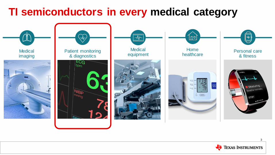
Home healthcare
Medical equipment
Patient monitoring & diagnostics
Medical imaging
TI semiconductors in every medical category
Personal care & fitness
3
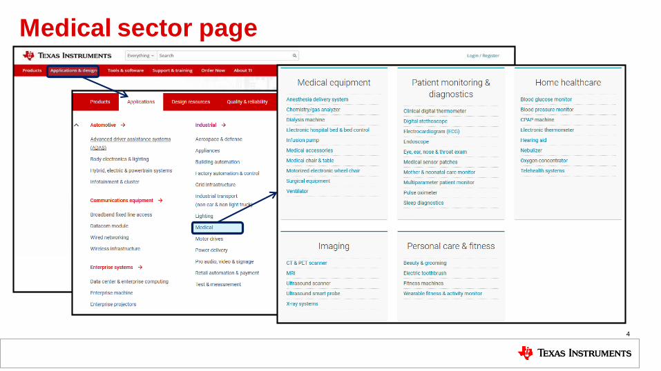
Medical sector page
4
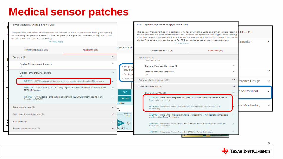
Medical sensor patches
5
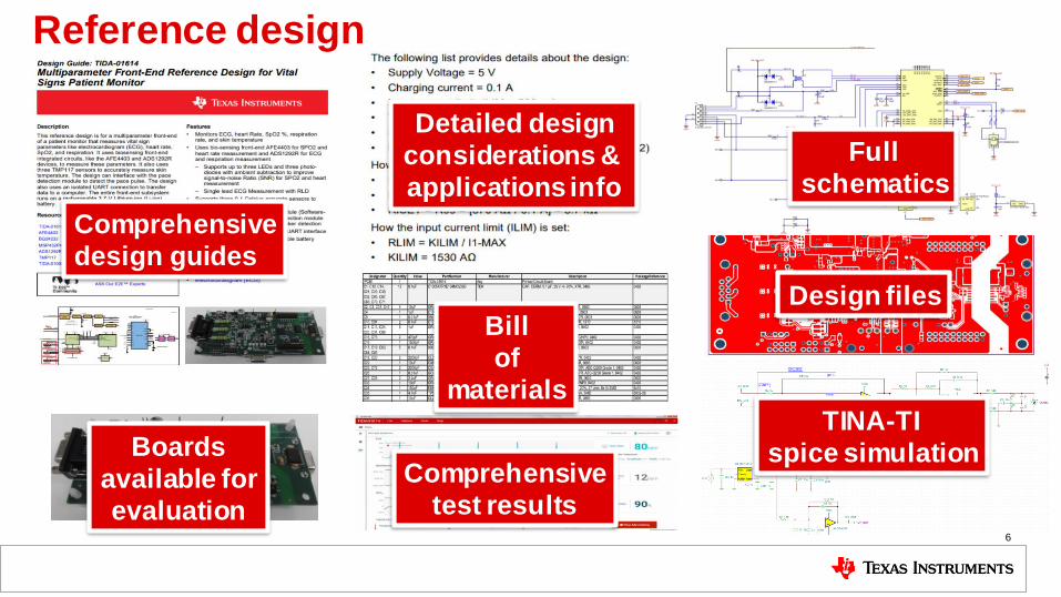
Reference design
Comprehensive
design guides
Detailed design
considerations &
applications info
Full
schematics
Design files
TINA-TI
spice simulation
Bill
of
materials
Comprehensive
test results
Boards
available for
evaluation6
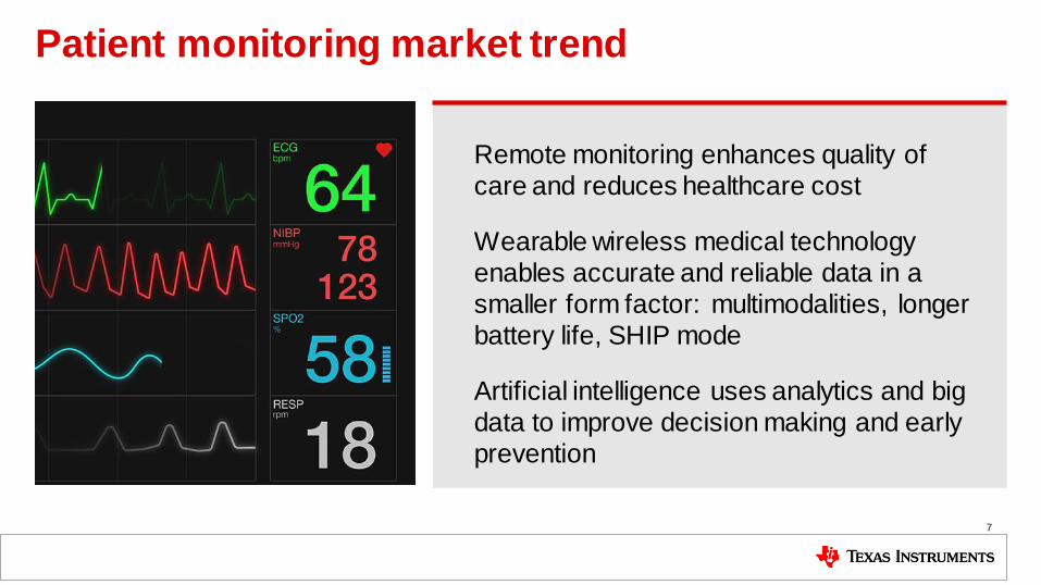
Patient monitoring market trend
7
Remote monitoring enhances quality of
care and reduces healthcare cost
Wearable wireless medical technology
enables accurate and reliable data in a
smaller form factor: multimodalities, longer
battery life, SHIP mode
Artificial intelligence uses analytics and big
data to improve decision making and early
prevention
Patient monitoring basics
8
Arterial
volume
1 Heartbeat
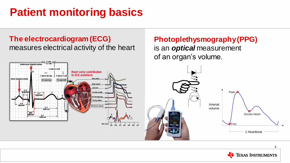
The electrocardiogram (ECG)
measures electrical activity of the heartPhotoplethysmography (PPG)
is an optical measurement
of an organ’s volume.
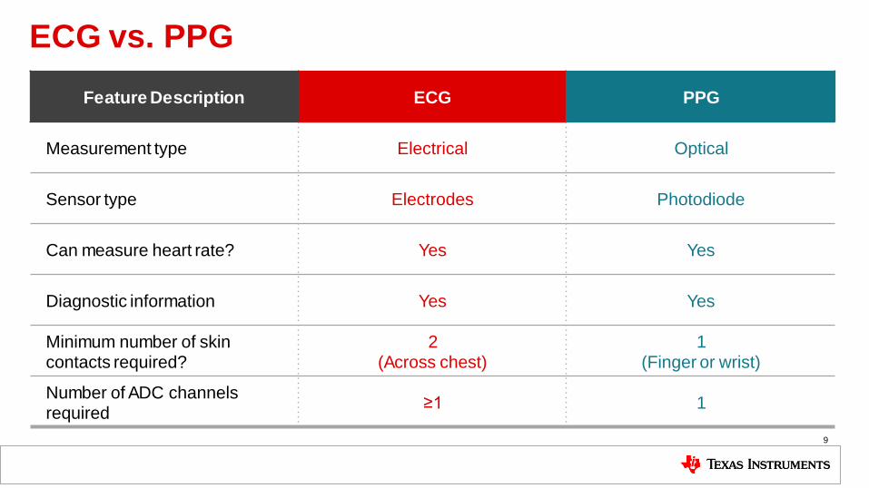
ECG vs. PPG
9
Feature Description ECG PPG
Measurement type Electrical Optical
Sensor type Electrodes Photodiode
Can measure heart rate? Yes Yes
Diagnostic information Yes Yes
Minimum number of skin contacts required?
2(Across chest)
1(Finger or wrist)
Number of ADC channels required
≥1 1
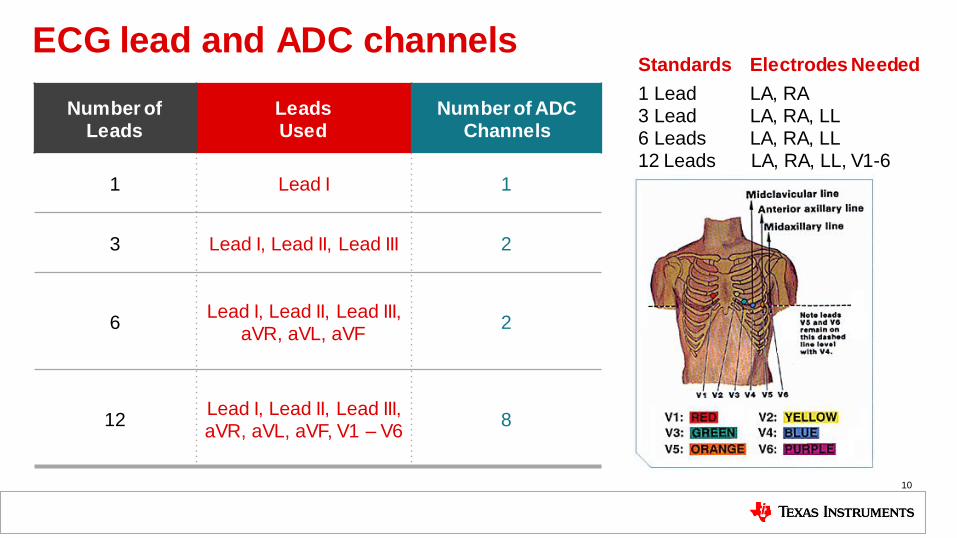
ECG lead and ADC channels
10
Standards Electrodes Needed
1 Lead LA, RA3 Lead LA, RA, LL6 Leads LA, RA, LL12 Leads LA, RA, LL, V1-6
Number of Leads
Leads Used
Number of ADC Channels
1 Lead I 1
3 Lead I, Lead II, Lead III 2
6Lead I, Lead II, Lead III,
aVR, aVL, aVF2
12Lead I, Lead II, Lead III, aVR, aVL, aVF, V1 – V6
8
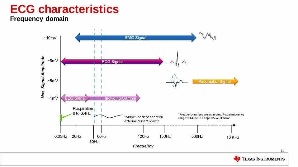
ECG characteristicsFrequency domain
11
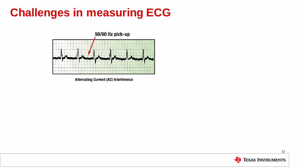
Challenges in measuring ECG
12
Challenges in optical bio-sensing
• Low power for longer battery life
• Skin tone variation
• Best PPG signal for motion cancellation algorithms
• Performance with glass
• Low temperature performance
• Ambient light
13
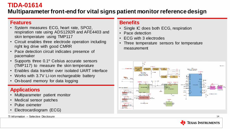
TIDA-01614Multiparameter front-end for vital signs patient monitor reference design
Benefits• Single IC does both ECG, respiration
• Pace detection
• ECG with 3 electrodes
• Three temperature sensors for temperature
measurement
Features• System measures ECG, heart rate, SPO2,
respiration rate using ADS1292R and AFE4403 and skin temperature using TMP117
• Circuit enables three electrode operation including right leg drive with good CMRR
• Pace detection circuit indicates presence of pacemaker
• Supports three 0.1º Celsius accurate sensors (TMP117) to measure the skin temperature
• Enables data transfer over isolated UART interface
• Works with 3.7V Li-ion rechargeable battery
• On-board memory for data logging
Applications• Multiparameter patient monitor
• Medical sensor patches
• Pulse oximeter
• Electrocardiogram (ECG)
14TI Information – Selective Disclosure
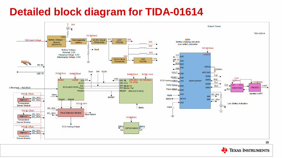
Detailed block diagram for TIDA-01614
1515
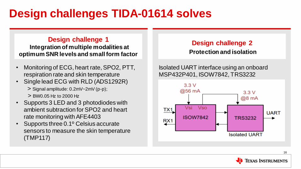
Design challenges TIDA-01614 solves
16
Design challenge 2
Protection and isolation
Design challenge 1Integration of multiple modalities at
optimum SNR levels and small form factor
• Monitoring of ECG, heart rate, SPO2, PTT, respiration rate and skin temperature
• Single lead ECG with RLD (ADS1292R) > Signal amplitude: 0.2mV~2mV (p-p);
> BW0.05 Hz to 2000 Hz
• Supports 3 LED and 3 photodiodes with ambient subtraction for SPO2 and heart rate monitoring with AFE4403
• Supports three 0.1º Celsius accurate sensors to measure the skin temperature (TMP117)
Isolated UART interface using an onboard MSP432P401, ISOW7842, TRS3232
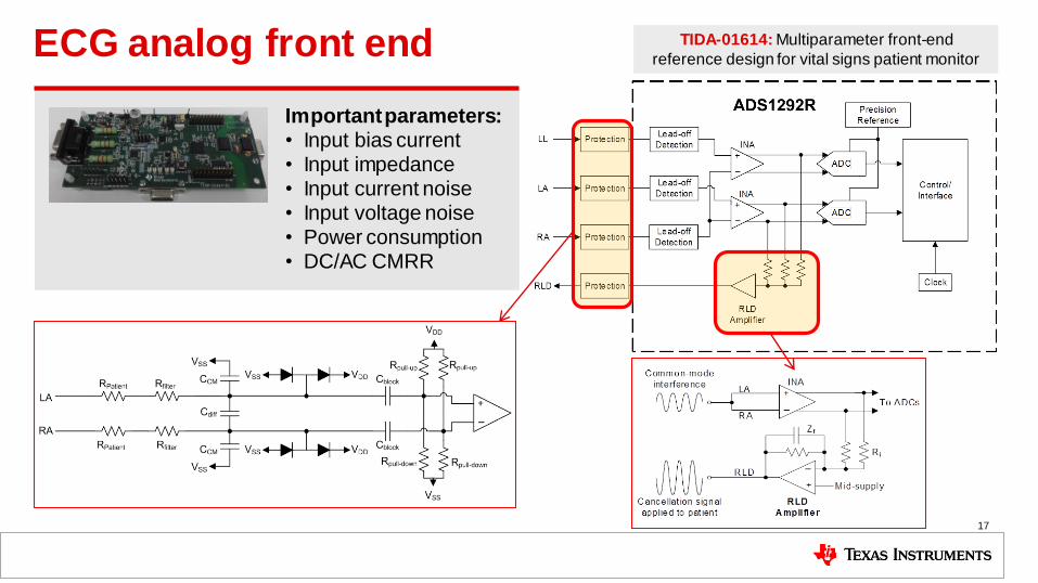
ECG analog front end
17
TIDA-01614: Multiparameter front-end
reference design for vital signs patient monitor
Important parameters:• Input bias current• Input impedance• Input current noise• Input voltage noise• Power consumption• DC/AC CMRR
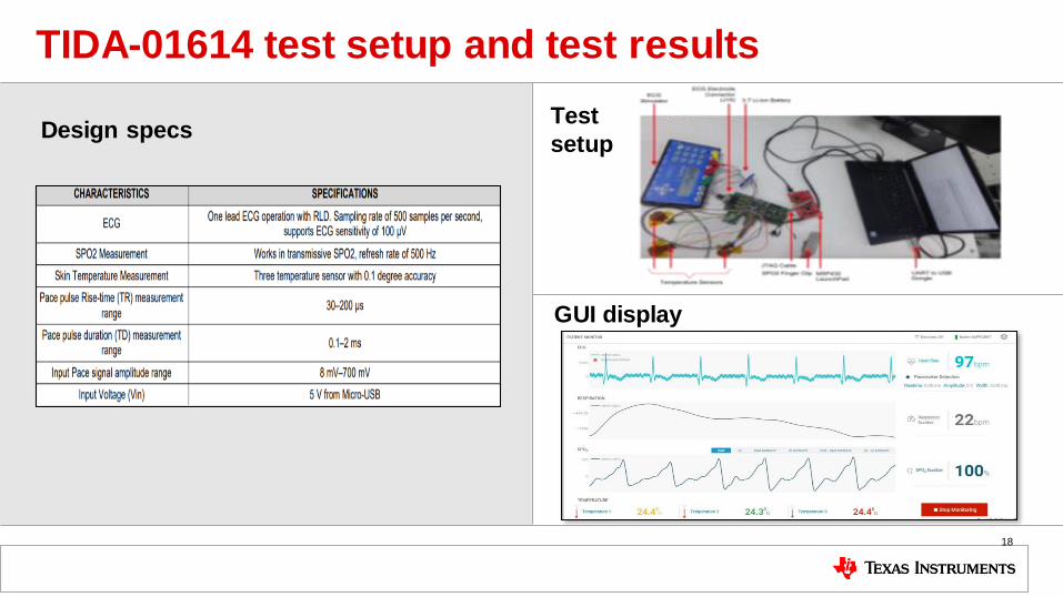
TIDA-01614 test setup and test results
18
Test
setup
GUI display
Design specs
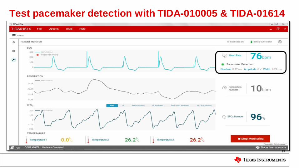
Test pacemaker detection with TIDA-010005 & TIDA-01614
19
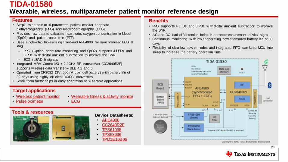
Device Datasheets:• AFE4900• CC2640R2F• TPS61098• TPS63036• TPD1E10B06
TIDA-01580 Wearable, wireless, multiparameter patient monitor reference design
• PPG supports 4 LEDs and 3 PDs w ith digital ambient subtraction to improve
the SNR
• AC and DC lead off detection helps in correct measurement of vital signs
• Continuous monitoring w ith low er operating pow er ensures battery life of 30
days
• Flexibility of ultra low pow er modes and integrated FIFO can keep MCU into
sleep to increase the battery operation time
• Simple w earable multi-parameter patient monitor for photo-
plethysmography (PPG) and electrocardiography (ECG)
• Provides raw data to calculate heart-rate, oxygen concentration in blood
(SpO2) and pulse-transit time (PTT)
• Uses single-chip bio-sensing front-end AFE4900 for synchronized ECG &
PPG
‒ PPG (Optical heart-rate monitoring and SpO2) supports 4 LEDs and
3 PDs w ith digital ambient subtraction to improve the SNR
‒ ECG (LEAD I) signals
• Integrated ARM Cortex-M3 + 2.4GHz RF transceiver (CC2640R2F)
supports w ireless data transfer – BLE 4.2 and 5
• Operated from CR3032 (3V, 500mA coin cell battery) w ith battery life of
30 days using highly eff icient DC/DC converters
• Small form factor helps in easy adaptation to w earable applications
Features Benefits
• Wireless patient monitor• Pulse oximeter
Target applications
Tools & resources
20
• Wearable fitness & activity monitor• ECG
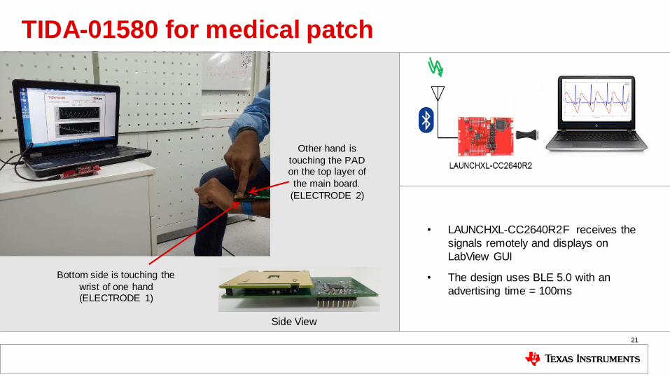
TIDA-01580 for medical patch
21
Bottom side is touching the
wrist of one hand (ELECTRODE 1)
Other hand is
touching the PAD on the top layer of
the main board.
(ELECTRODE 2)
Side View
• LAUNCHXL-CC2640R2F receives the
signals remotely and displays on
LabView GUI
• The design uses BLE 5.0 with an
advertising time = 100ms
22
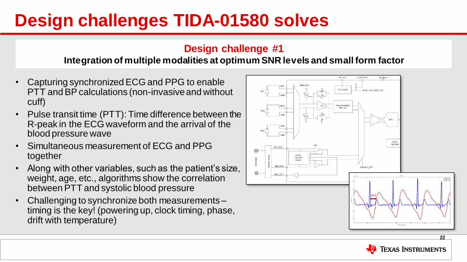
Design challenge #1Integration of multiple modalities at optimum SNR levels and small form factor
• Capturing synchronized ECG and PPG to enable PTT and BP calculations (non-invasive and without cuff)
• Pulse transit time (PTT): Time difference between the R-peak in the ECG waveform and the arrival of the blood pressure wave
• Simultaneous measurement of ECG and PPG together
• Along with other variables, such as the patient’s size, weight, age, etc., algorithms show the correlation between PTT and systolic blood pressure
• Challenging to synchronize both measurements –timing is the key! (powering up, clock timing, phase, drift with temperature)
Design challenges TIDA-01580 solves
22
23
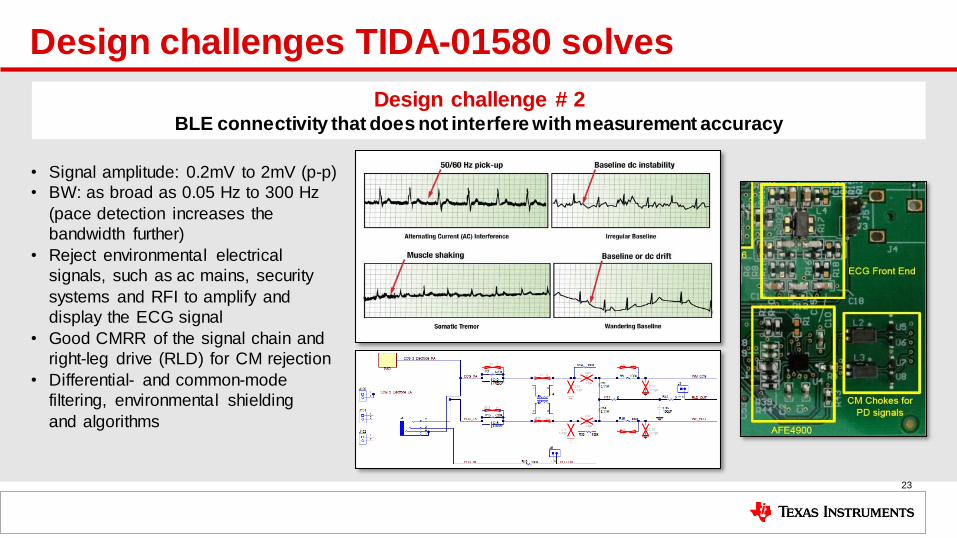
Design challenge # 2 BLE connectivity that does not interfere with measurement accuracy
• Signal amplitude: 0.2mV to 2mV (p-p)
• BW: as broad as 0.05 Hz to 300 Hz
(pace detection increases the
bandwidth further)
• Reject environmental electrical
signals, such as ac mains, security
systems and RFI to amplify and
display the ECG signal
• Good CMRR of the signal chain and
right-leg drive (RLD) for CM rejection
• Differential- and common-mode
filtering, environmental shielding
and algorithms
Design challenges TIDA-01580 solves
Design challenge # 3 Extending battery life to multiple days to enable portability & wearability
24
• Selecting the right power architecture to enable extended battery life up to 24 hours (for rechargeable batteries) or 7 days (for primary cells)
• Powering with right buck, boost or buck-boost device instead of directly powering from battery (bypass modes in DC/DC converters)
• Sleep / shutdown / standby / deep sleep modes for radio devices like BLE, Wi-Fi etc.
• Selection of right battery charger (charging rate, termination current and quiescent currents are important!)
Design challenges TIDA-01580 solves
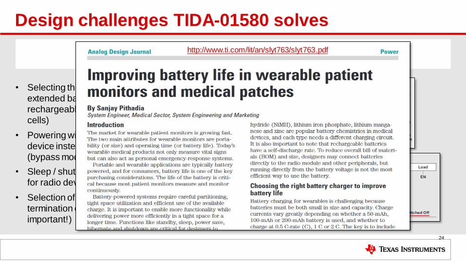
http://www.ti.com/lit/an/slyt763/slyt763.pdf
• TIDA-01624 and/or tools
folder
• Design guide
• Design files: Schematics,
BOM, Gerbers, Software, etc.
• Device datasheets:‒ TMP117
‒ CC2640R2F
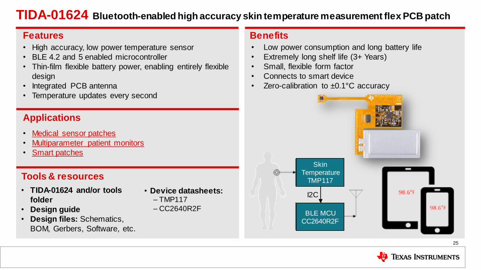
TIDA-01624 Bluetooth-enabled high accuracy skin temperature measurement flex PCB patch
• Low power consumption and long battery life
• Extremely long shelf life (3+ Years)
• Small, flexible form factor
• Connects to smart device
• Zero-calibration to ±0.1°C accuracy
• High accuracy, low power temperature sensor
• BLE 4.2 and 5 enabled microcontroller
• Thin-film flexible battery power, enabling entirely flexible
design
• Integrated PCB antenna
• Temperature updates every second
Features Benefits
Tools & resources
• Medical sensor patches
• Multiparameter patient monitors
• Smart patches
Applications
Skin Temperature
TMP117
BLE MCUCC2640R2F
I2C
25
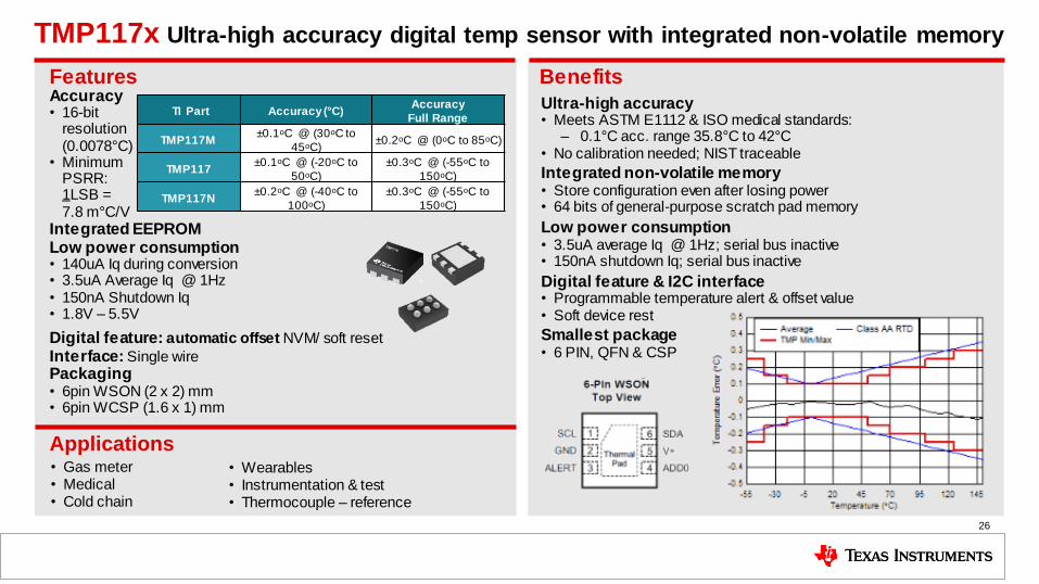
Ultra-high accuracy• Meets ASTM E1112 & ISO medical standards:
‒ 0.1°C acc. range 35.8°C to 42°C• No calibration needed; NIST traceable
Integrated non-volatile memory• Store configuration even after losing power• 64 bits of general-purpose scratch pad memory
Low power consumption• 3.5uA average Iq @ 1Hz; serial bus inactive• 150nA shutdown Iq; serial bus inactive
Digital feature & I2C interface• Programmable temperature alert & offset value• Soft device rest
Smallest package • 6 PIN, QFN & CSP
Features Benefits
TMP117x Ultra-high accuracy digital temp sensor with integrated non-volatile memory
Accuracy• 16-bit
resolution (0.0078°C)
• Minimum PSRR: 1LSB = 7.8 m°C/V
Integrated EEPROMLow power consumption • 140uA Iq during conversion• 3.5uA Average Iq @ 1Hz• 150nA Shutdown Iq• 1.8V – 5.5V
Digital feature: automatic offset NVM/ soft reset
Interface: Single wire Packaging• 6pin WSON (2 x 2) mm• 6pin WCSP (1.6 x 1) mm
• Gas meter• Medical• Cold chain
• Wearables• Instrumentation & test • Thermocouple – reference
Applications
TI Part Accuracy (°C)Accuracy
Full Range
TMP117M±0.1oC @ (30oC to
45oC)±0.2oC @ (0oC to 85oC)
TMP117±0.1oC @ (-20oC to
50oC)
±0.3oC @ (-55oC to
150oC)
TMP117N±0.2oC @ (-40oC to
100oC)
±0.3oC @ (-55oC to
150oC)
26
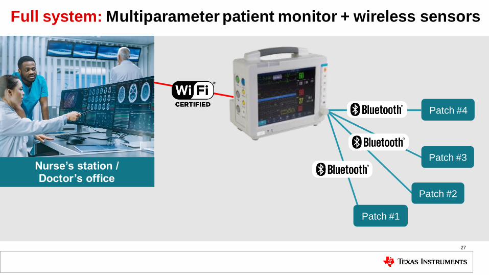
Full system: Multiparameter patient monitor + wireless sensors
27
Patch #1
Patch #2
Patch #3
Patch #4
Nurse’s station / Doctor’s office
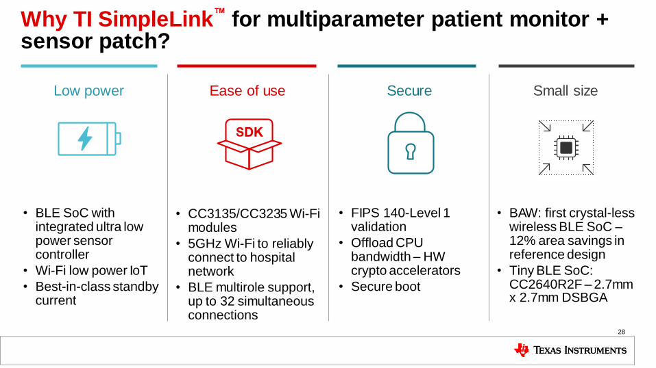
Why TI SimpleLink™ for multiparameter patient monitor + sensor patch?
28
• BLE SoC with integrated ultra low power sensor controller
• Wi-Fi low power IoT
• Best-in-class standby current
• CC3135/CC3235 Wi-Fi modules
• 5GHz Wi-Fi to reliably connect to hospital network
• BLE multirole support, up to 32 simultaneous connections
• FIPS 140-Level 1 validation
• Offload CPU bandwidth – HW crypto accelerators
• Secure boot
• BAW: first crystal-less wireless BLE SoC –12% area savings in reference design
• Tiny BLE SoC: CC2640R2F – 2.7mm x 2.7mm DSBGA
Secure Small sizeEase of useLow power
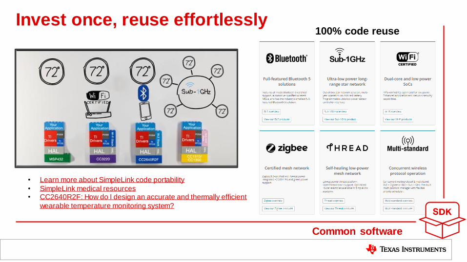
Invest once, reuse effortlessly
29
• Learn more about SimpleLink code portability
• SimpleLink medical resources• CC2640R2F: How do I design an accurate and thermally efficient
wearable temperature monitoring system?
100% code reuse
Common software
Achieve isolation and help enable patient safety
30
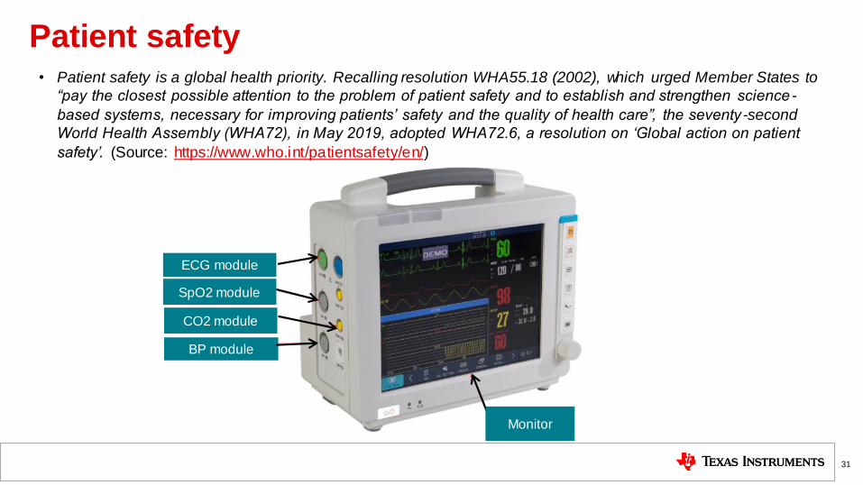
Patient safety• Patient safety is a global health priority. Recalling resolution WHA55.18 (2002), which urged Member States to
“pay the closest possible attention to the problem of patient safety and to establish and strengthen science -
based systems, necessary for improving patients’ safety and the quality of health care”, the seventy -second
World Health Assembly (WHA72), in May 2019, adopted WHA72.6, a resolution on ‘Global action on patient
safety’. (Source: https://www.who.int/patientsafety/en/)
ECG module
SpO2 module
CO2 module
BP module
Monitor
31
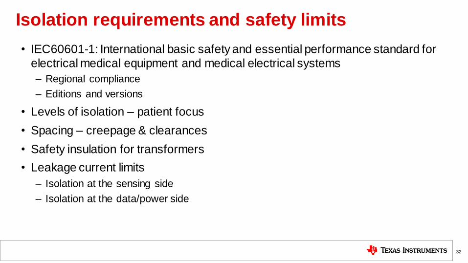
Isolation requirements and safety limits
• IEC60601-1: International basic safety and essential performance standard for
electrical medical equipment and medical electrical systems
– Regional compliance
– Editions and versions
• Levels of isolation – patient focus
• Spacing – creepage & clearances
• Safety insulation for transformers
• Leakage current limits
– Isolation at the sensing side
– Isolation at the data/power side
32
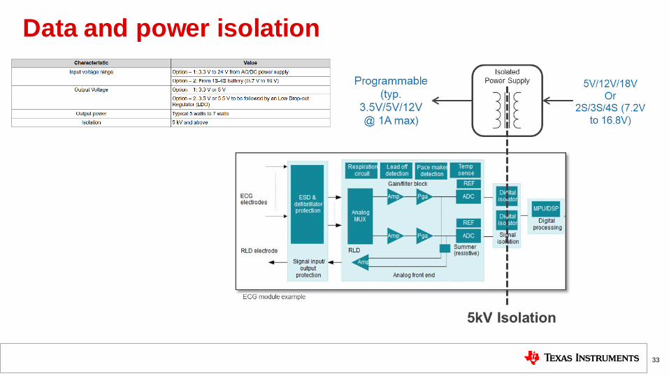
Data and power isolation
33
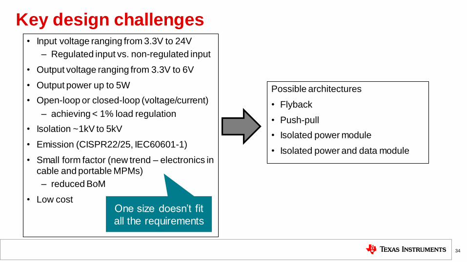
Key design challenges• Input voltage ranging from 3.3V to 24V
– Regulated input vs. non-regulated input
• Output voltage ranging from 3.3V to 6V
• Output power up to 5W
• Open-loop or closed-loop (voltage/current)
– achieving < 1% load regulation
• Isolation ~1kV to 5kV
• Emission (CISPR22/25, IEC60601-1)
• Small form factor (new trend – electronics in cable and portable MPMs)
– reduced BoM
• Low costOne size doesn’t fit
all the requirements
Possible architectures
• Flyback
• Push-pull
• Isolated power module
• Isolated power and data module
34
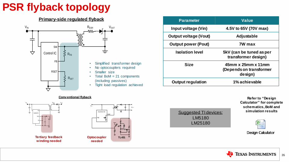
PSR flyback topology
VIN VOUT
BIAS
FB
SW
Control IC
RESR
Tertiary feedback
winding neededOptocoupler
needed
TL431
Parameter Value
Input voltage (Vin) 4.5V to 65V (70V max)
Output voltage (Vout) Adjustable
Output power (Pout) 7W max
Isolation level 5kV (can be tuned as per transformer design)
Size 45mm x 25mm x 11mm (Depends on transformer
design)
Output regulation 1% achievable
Suggested TI devices:
LM5180LM25180
Conv entional flyback
VIN VOUT
FB
RSET
SW
Control IC
RESR
RFB
RSET
• Simplif ied transformer design
• No optocouplers required
• Smaller size
• Total BoM = 21 components
(including passives)
• Tight load regulation achieved
Primary-side regulated flyback
Refer to “Design
Calculator” for complete
schematics, BoM and
simulation results
35
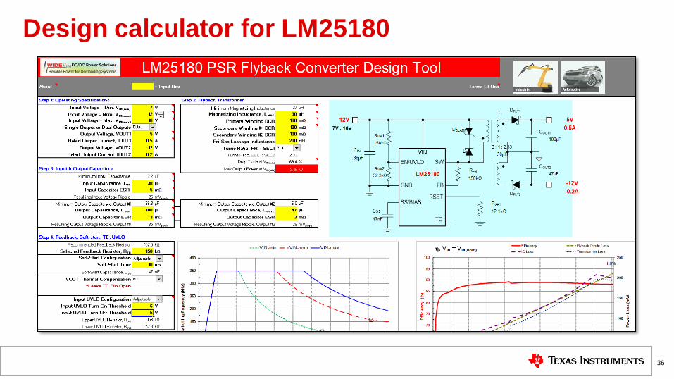
Design calculator for LM25180
36
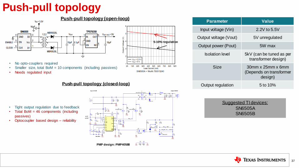
Push-pull topology
• Tight output regulation due to feedback
• Total BoM = 46 components (including
passives)
• Optocoupler based design – reliability
Push-pull topology (closed-loop)
Push-pull topology (open-loop)
PMP design: PMP40588
5-10% regulation
• No opto-couplers required
• Smaller size, total BoM = 10 components (including passives)
• Needs regulated input
Parameter Value
Input voltage (Vin) 2.2V to 5.5V
Output voltage (Vout) 5V unregulated
Output power (Pout) 5W max
Isolation level 5kV (can be tuned as per transformer design)
Size 30mm x 25mm x 6mm (Depends on transformer
design)
Output regulation 5 to 10%
Suggested TI devices:
SN6505ASN6505B
37
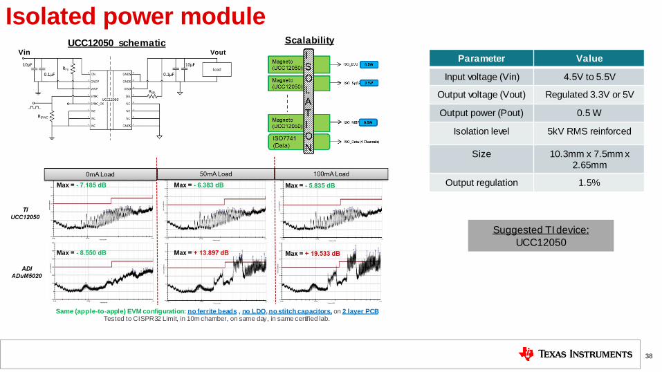
Isolated power module
Vin Vout
Suggested TI device:
UCC12050
Same (apple-to-apple) EVM configuration: no ferrite beads , no LDO, no stitch capacitors, on 2 layer PCBTested to CISPR32 Limit, in 10m chamber, on same day, in same certified lab.
UCC12050 schematic Scalability
Parameter Value
Input voltage (Vin) 4.5V to 5.5V
Output voltage (Vout) Regulated 3.3V or 5V
Output power (Pout) 0.5 W
Isolation level 5kV RMS reinforced
Size 10.3mm x 7.5mm x 2.65mm
Output regulation 1.5%
38
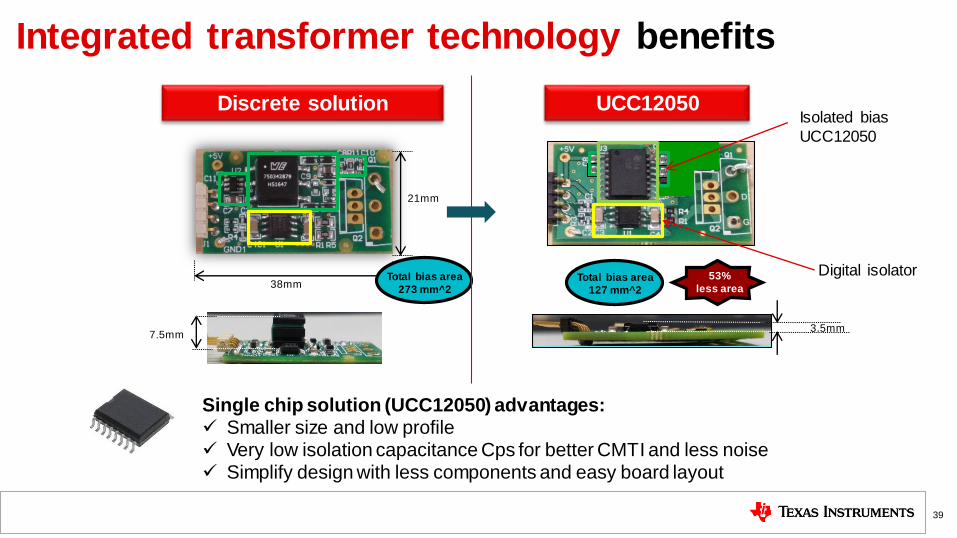
Integrated transformer technology benefits
Discrete solution
38mm
21mm
7.5mm
Total bias area
273 mm^2
53%
less areaTotal bias area
127 mm^2
UCC12050
3.5mm
Single chip solution (UCC12050) advantages:✓ Smaller size and low profile✓ Very low isolation capacitance Cps for better CMTI and less noise✓ Simplify design with less components and easy board layout
Digital isolator
Isolated bias
UCC12050
39
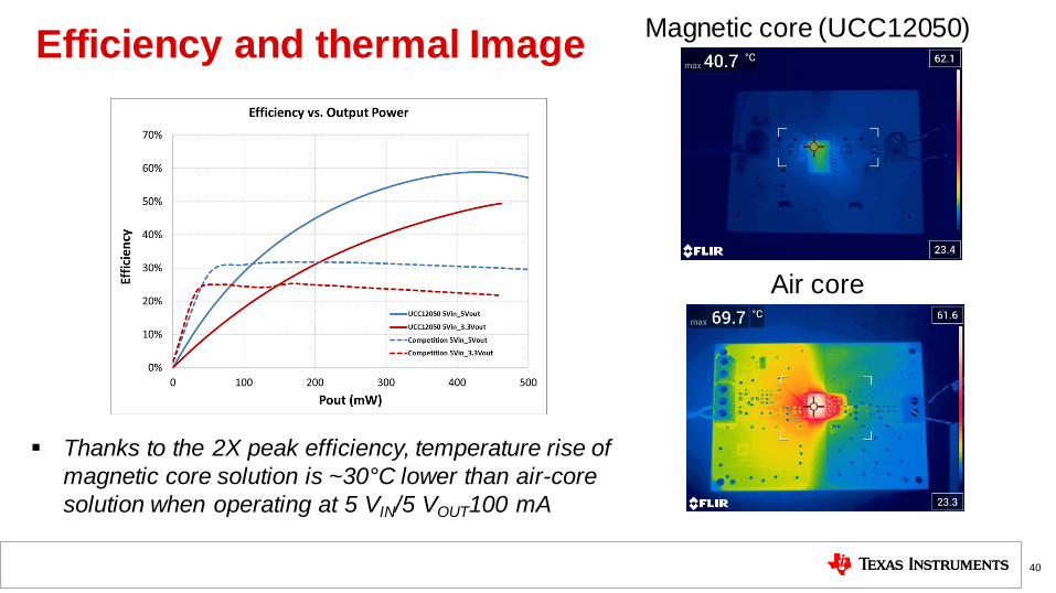
Efficiency and thermal Image
Air core
Magnetic core (UCC12050)
▪ Thanks to the 2X peak efficiency, temperature rise of
magnetic core solution is ~30°C lower than air-core
solution when operating at 5 VIN/5 VOUT100 mA
40
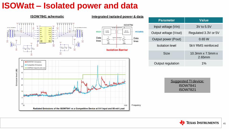
ISOWatt – Isolated power and data
Suggested TI device:
ISOW7841ISOW7821
ISOW7841 schematic Integrated isolated power & dataParameter Value
Input voltage (Vin) 3V to 5.5V
Output voltage (Vout) Regulated 3.3V or 5V
Output power (Pout) 0.65 W
Isolation level 5kV RMS reinforced
Size 10.3mm x 7.5mm x 2.65mm
Output regulation 1%
Frequency
Em
issio
n level (d
B)
41
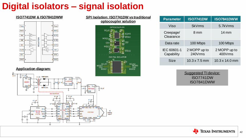
Digital isolators – signal isolation
Suggested TI device:
ISO7741DWISO7841DWW
ISO7741DW & ISO7841DWW
Application diagram:
Parameter ISO7741DW ISO7841DWW
Viso 5kVrms 5.7kVrms
Creepage/ Clearance
8 mm 14 mm
Data rate 100 Mbps 100 Mbps
IEC 60601-1 Capability
2 MOPP up to 240Vrms
2 MOPP up to 400Vrms
Size 10.3 x 7.5 mm 10.3 x 14.0 mm
SPI Isolation: ISO7741DW vs traditional optocoupler solution
42
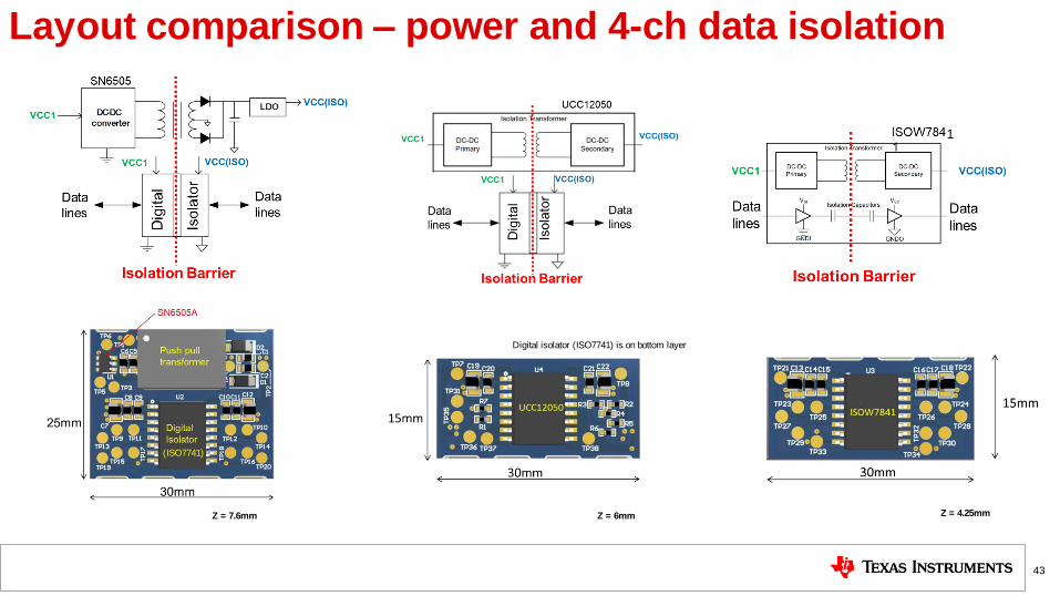
Layout comparison – power and 4-ch data isolation
Digital isolator (ISO7741) is on bottom layer
1
(ISO7741)
Z = 4.25mmZ = 6mmZ = 7.6mm
43
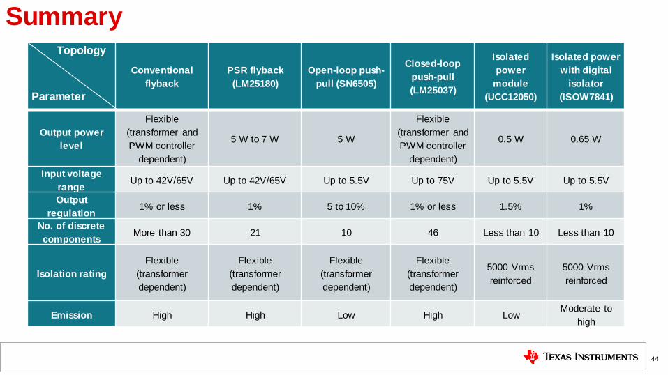
Summary Topology
Parameter
Conventional
flyback
PSR flyback
(LM25180)
Open-loop push-
pull (SN6505)
Closed-loop
push-pull
(LM25037)
Isolated
power
module
(UCC12050)
Isolated power
with digital
isolator
(ISOW7841)
Output power
level
Flexible
(transformer and
PWM controller
dependent)
5 W to 7 W 5 W
Flexible
(transformer and
PWM controller
dependent)
0.5 W 0.65 W
Input voltage
rangeUp to 42V/65V Up to 42V/65V Up to 5.5V Up to 75V Up to 5.5V Up to 5.5V
Output
regulation 1% or less 1% 5 to 10% 1% or less 1.5% 1%
No. of discrete
componentsMore than 30 21 10 46 Less than 10 Less than 10
Isolation rating
Flexible
(transformer
dependent)
Flexible
(transformer
dependent)
Flexible
(transformer
dependent)
Flexible
(transformer
dependent)
5000 Vrms
reinforced
5000 Vrms
reinforced
Emission High High Low High LowModerate to
high
44
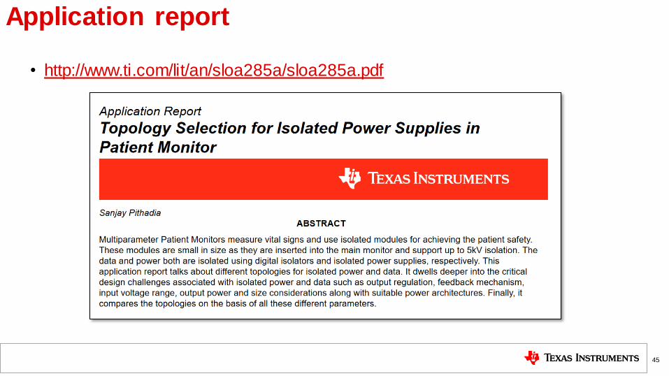
Application report
• http://www.ti.com/lit/an/sloa285a/sloa285a.pdf
45
46
©2021 Texas Instruments Incorporated. All rights reserved.
SLYP747

IMPORTANT NOTICE AND DISCLAIMERTI PROVIDES TECHNICAL AND RELIABILITY DATA (INCLUDING DATASHEETS), DESIGN RESOURCES (INCLUDING REFERENCEDESIGNS), APPLICATION OR OTHER DESIGN ADVICE, WEB TOOLS, SAFETY INFORMATION, AND OTHER RESOURCES “AS IS”AND WITH ALL FAULTS, AND DISCLAIMS ALL WARRANTIES, EXPRESS AND IMPLIED, INCLUDING WITHOUT LIMITATION ANYIMPLIED WARRANTIES OF MERCHANTABILITY, FITNESS FOR A PARTICULAR PURPOSE OR NON-INFRINGEMENT OF THIRDPARTY INTELLECTUAL PROPERTY RIGHTS.These resources are intended for skilled developers designing with TI products. You are solely responsible for (1) selecting the appropriateTI products for your application, (2) designing, validating and testing your application, and (3) ensuring your application meets applicablestandards, and any other safety, security, or other requirements. These resources are subject to change without notice. TI grants youpermission to use these resources only for development of an application that uses the TI products described in the resource. Otherreproduction and display of these resources is prohibited. No license is granted to any other TI intellectual property right or to any third partyintellectual property right. TI disclaims responsibility for, and you will fully indemnify TI and its representatives against, any claims, damages,costs, losses, and liabilities arising out of your use of these resources.TI’s products are provided subject to TI’s Terms of Sale (https:www.ti.com/legal/termsofsale.html) or other applicable terms available eitheron ti.com or provided in conjunction with such TI products. TI’s provision of these resources does not expand or otherwise alter TI’sapplicable warranties or warranty disclaimers for TI products.IMPORTANT NOTICE
Mailing Address: Texas Instruments, Post Office Box 655303, Dallas, Texas 75265Copyright © 2021, Texas Instruments Incorporated


![Wearable Sensing Electronics for Healthcare Applications · 2019. 3. 11. · properties are tuned according to the processing requirements of the respective printing technology [32]](https://img.pdfslide.net/doc/110x75/60a15539871a0305905e9864/wearable-sensing-electronics-for-healthcare-applications-2019-3-11-properties.jpg)