Embed Size (px)
Citation preview
Manuscript for DesignCon 2006, February 6-9, 2006, Santa Clara, CA
DesignCon 2006
Attenuation in PCB Traces due to Periodic Discontinuities Gustavo Blando, Sun Microsystems Jason Miller, Sun Microsystems Istvan Novak, Sun Microsystems Jim DeLap, Ansoft Corp. Cheryl Preston, Sun Microsystems

Manuscript for DesignCon 2006, February 6-9, 2006, Santa Clara, CA
Abstract Beyond the traditional components of conductive and dielectric losses, periodic discontinuities generate additional losses on interconnects. For instance, on printed-circuit boards (PCBs) and packages, periodic discontinuities may come from perforated planes and loading from regularly arranged via fields under large packages and sockets. There is an increased slope of attenuation with frequency due to periodic losses, with deeper resonant dips at frequencies where the periodic structure constructively lines up reflections. The frequencies where the dips occur are lower if the propagation delay between subsequent discontinuities is longer. The depth of the dips depends on how severe the discontinuities are. The paper provides measured and simulated data of this extra loss mechanism, together with simulated studies examining the impact of several geometrical parameters. Author(s) Biography Gustavo Blando is a signal Integrity engineer with over 10 years of experience in the industry. Currently at Sun Microsystems he is responsible for the development of new processes and methodologies in the areas of broadband measurement, high speed modeling and system simulations. He received his M.S. from Northeastern University. Jason Miller is currently a Staff Engineer at Sun Microsystems where he works on ASIC development, ASIC packaging, interconnect modeling and characterization, and system simulation. He received his Ph.D. in Electrical Engineering from Columbia University. Istvan Novak is a signal-integrity senior staff engineer at Sun Microsystems, Inc. Besides signal integrity design of high-speed serial and parallel buses, he is engaged in the design and characterization of power-distribution networks and packages for Sun servers. He creates simulation models, and develops measurement techniques for power distribution. Istvan has twenty plus years of experience with high-speed digital, RF and analog circuits, and system design. He is a Fellow of IEEE for his contributions to the fields of signal-integrity, RF measurements, and simulation methodologies. Jim DeLap is an Applications Engineer specializing in the High Frequency products including HFSS and Ansoft Designer. Prior to working at Ansoft, he has designed many products ranging from millimeter-wave mixers and antennas to integrated radios in the 30-60 GHz range. He earned his B.S. in Electrical Engineering from the University of Lowell, Lowell, MA, his M.S. in Electrical Engineering from the University of Virginia, Charlottesville, VA, and has worked for companies such as Millitech Corporation, Raytheon, and Agilent Technologies. Cheryl Preston is a Staff Engineer at Sun Microsystems with over 20 years of industry experience.
Manuscript for DesignCon 2006, February 6-9, 2006, Santa Clara, CA
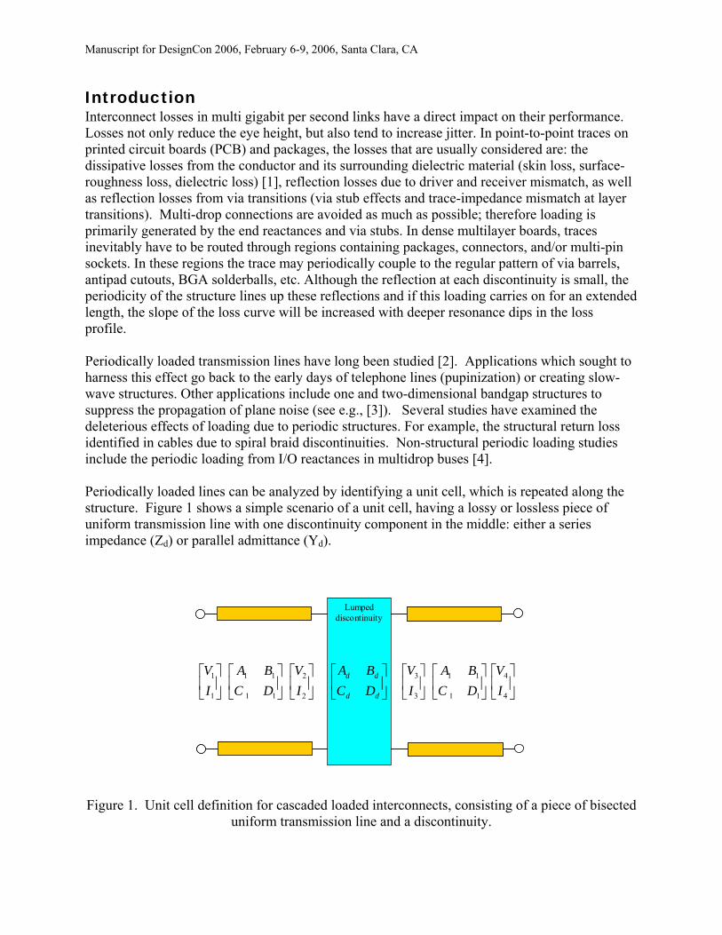
Introduction Interconnect losses in multi gigabit per second links have a direct impact on their performance. Losses not only reduce the eye height, but also tend to increase jitter. In point-to-point traces on printed circuit boards (PCB) and packages, the losses that are usually considered are: the dissipative losses from the conductor and its surrounding dielectric material (skin loss, surface-roughness loss, dielectric loss) [1], reflection losses due to driver and receiver mismatch, as well as reflection losses from via transitions (via stub effects and trace-impedance mismatch at layer transitions). Multi-drop connections are avoided as much as possible; therefore loading is primarily generated by the end reactances and via stubs. In dense multilayer boards, traces inevitably have to be routed through regions containing packages, connectors, and/or multi-pin sockets. In these regions the trace may periodically couple to the regular pattern of via barrels, antipad cutouts, BGA solderballs, etc. Although the reflection at each discontinuity is small, the periodicity of the structure lines up these reflections and if this loading carries on for an extended length, the slope of the loss curve will be increased with deeper resonance dips in the loss profile. Periodically loaded transmission lines have long been studied [2]. Applications which sought to harness this effect go back to the early days of telephone lines (pupinization) or creating slow-wave structures. Other applications include one and two-dimensional bandgap structures to suppress the propagation of plane noise (see e.g., [3]). Several studies have examined the deleterious effects of loading due to periodic structures. For example, the structural return loss identified in cables due to spiral braid discontinuities. Non-structural periodic loading studies include the periodic loading from I/O reactances in multidrop buses [4]. Periodically loaded lines can be analyzed by identifying a unit cell, which is repeated along the structure. Figure 1 shows a simple scenario of a unit cell, having a lossy or lossless piece of uniform transmission line with one discontinuity component in the middle: either a series impedance (Zd) or parallel admittance (Yd).
Lumped discontinuity
⎥⎦
⎤⎢⎣
⎡⎥⎦
⎤⎢⎣
⎡⎥⎦
⎤⎢⎣
⎡⎥⎦
⎤⎢⎣
⎡⎥⎦
⎤⎢⎣
⎡⎥⎦
⎤⎢⎣
⎡⎥⎦
⎤⎢⎣
⎡
4
4
11
11
3
3
2
2
11
11
1
1
IV
DCBA
IV
DCBA
IV
DCBA
IV
dd
dd
Figure 1. Unit cell definition for cascaded loaded interconnects, consisting of a piece of bisected
uniform transmission line and a discontinuity.
Manuscript for DesignCon 2006, February 6-9, 2006, Santa Clara, CA
Assuming an infinite number of cascaded unit cells, the complex propagation constant of one unit cell can be expressed with the propagation constant of the unloaded interconnect and the reactance of the parallel (Yd) or series (Zd) discontinuity, respectively:
(1)
where γ is the complex propagation constant of the unloaded interconnect, γp is the complex propagation constant of the periodically loaded interconnect, d is the length of the unit cell, Z0 is the characteristic impedance of the unloaded interconnect, Zd is the impedance of the series discontinuity, and Yd is the admittance of the parallel discontinuity.The overall transmission characteristics of the periodically loaded interconnect can be calculated by multiplying the ABCD matrices of the cascaded unit cells. The ABCD matrix of the unit cell with a series (Zd) discontinuity is [2]:
00
00
0
/}]1)){cosh(2/()[sinh(}]1)){cosh(2/()[sinh(
)sinh()2/()cosh(
ZdZZdCdZZdZBdZZdDA
d
d
d
−+=++=
+==
γγγγγγ
(2)
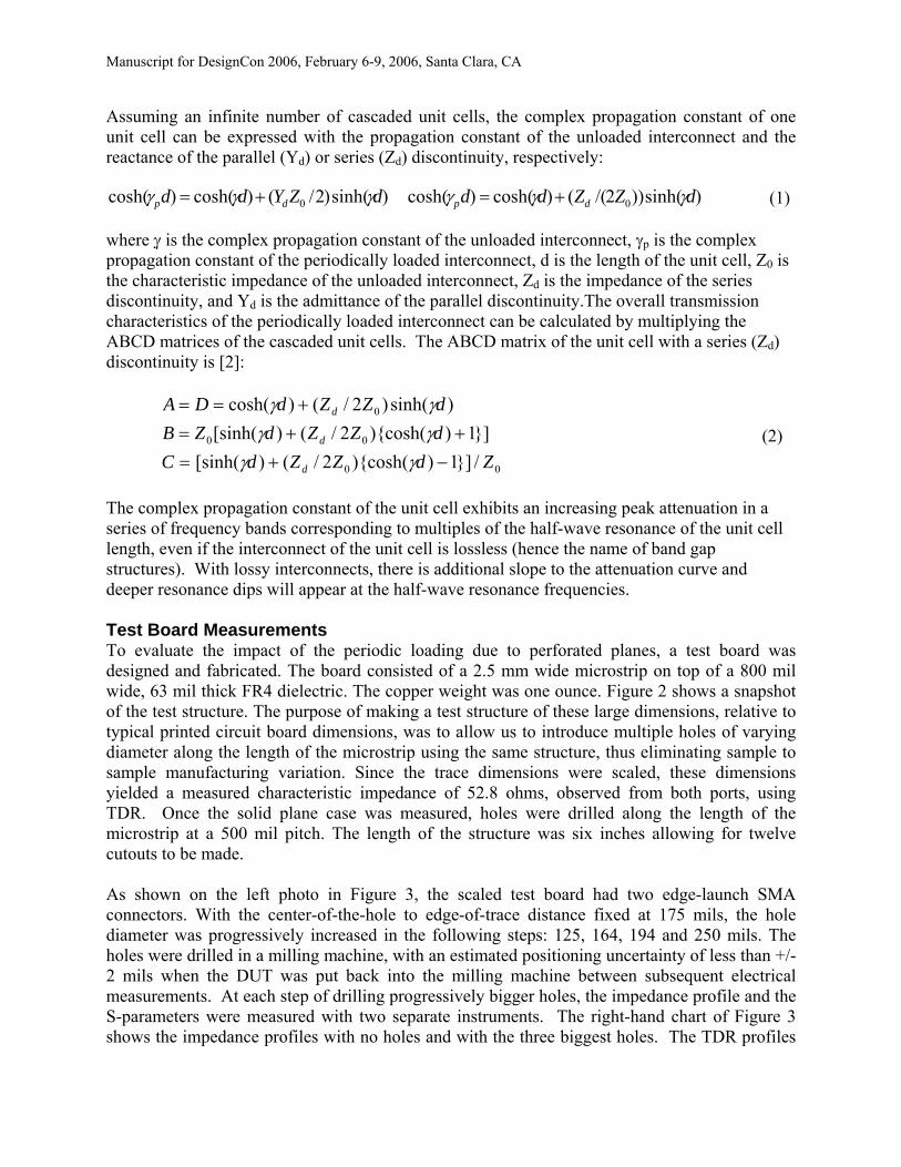
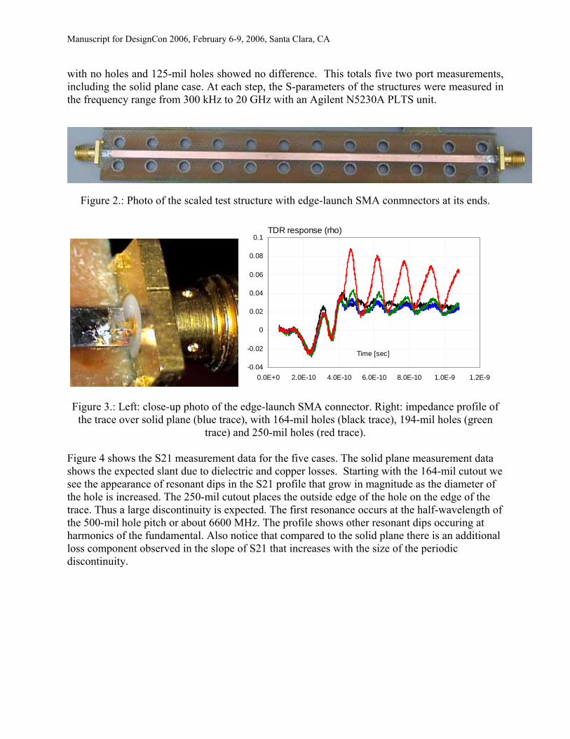
The complex propagation constant of the unit cell exhibits an increasing peak attenuation in a series of frequency bands corresponding to multiples of the half-wave resonance of the unit cell length, even if the interconnect of the unit cell is lossless (hence the name of band gap structures). With lossy interconnects, there is additional slope to the attenuation curve and deeper resonance dips will appear at the half-wave resonance frequencies. Test Board Measurements To evaluate the impact of the periodic loading due to perforated planes, a test board was designed and fabricated. The board consisted of a 2.5 mm wide microstrip on top of a 800 mil wide, 63 mil thick FR4 dielectric. The copper weight was one ounce. Figure 2 shows a snapshot of the test structure. The purpose of making a test structure of these large dimensions, relative to typical printed circuit board dimensions, was to allow us to introduce multiple holes of varying diameter along the length of the microstrip using the same structure, thus eliminating sample to sample manufacturing variation. Since the trace dimensions were scaled, these dimensions yielded a measured characteristic impedance of 52.8 ohms, observed from both ports, using TDR. Once the solid plane case was measured, holes were drilled along the length of the microstrip at a 500 mil pitch. The length of the structure was six inches allowing for twelve cutouts to be made. As shown on the left photo in Figure 3, the scaled test board had two edge-launch SMA connectors. With the center-of-the-hole to edge-of-trace distance fixed at 175 mils, the hole diameter was progressively increased in the following steps: 125, 164, 194 and 250 mils. The holes were drilled in a milling machine, with an estimated positioning uncertainty of less than +/- 2 mils when the DUT was put back into the milling machine between subsequent electrical measurements. At each step of drilling progressively bigger holes, the impedance profile and the S-parameters were measured with two separate instruments. The right-hand chart of Figure 3 shows the impedance profiles with no holes and with the three biggest holes. The TDR profiles
cosh(γpd) = cosh(γd)+ (YdZ0 /2)sinh(γd) cosh(γpd) = cosh(γd)+ (Zd /(2Z0))sinh(γd)
Manuscript for DesignCon 2006, February 6-9, 2006, Santa Clara, CA
with no holes and 125-mil holes showed no difference. This totals five two port measurements, including the solid plane case. At each step, the S-parameters of the structures were measured in the frequency range from 300 kHz to 20 GHz with an Agilent N5230A PLTS unit.
Figure 2.: Photo of the scaled test structure with edge-launch SMA conmnectors at its ends.
TDR response (rho)
-0.04
-0.02
0
0.02
0.04
0.06
0.08
0.1
0.0E+0 2.0E-10 4.0E-10 6.0E-10 8.0E-10 1.0E-9 1.2E-9
Time [sec]
Figure 3.: Left: close-up photo of the edge-launch SMA connector. Right: impedance profile of
the trace over solid plane (blue trace), with 164-mil holes (black trace), 194-mil holes (green trace) and 250-mil holes (red trace).
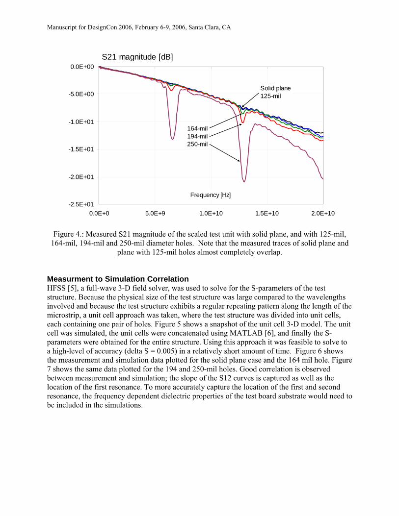
Figure 4 shows the S21 measurement data for the five cases. The solid plane measurement data shows the expected slant due to dielectric and copper losses. Starting with the 164-mil cutout we see the appearance of resonant dips in the S21 profile that grow in magnitude as the diameter of the hole is increased. The 250-mil cutout places the outside edge of the hole on the edge of the trace. Thus a large discontinuity is expected. The first resonance occurs at the half-wavelength of the 500-mil hole pitch or about 6600 MHz. The profile shows other resonant dips occuring at harmonics of the fundamental. Also notice that compared to the solid plane there is an additional loss component observed in the slope of S21 that increases with the size of the periodic discontinuity.
Manuscript for DesignCon 2006, February 6-9, 2006, Santa Clara, CA
S21 magnitude [dB]
-2.5E+01
-2.0E+01
-1.5E+01
-1.0E+01
-5.0E+00
0.0E+00
0.0E+0 5.0E+9 1.0E+10 1.5E+10 2.0E+10
Frequency [Hz]
164-mil194-mil250-mil
Solid plane125-mil
Figure 4.: Measured S21 magnitude of the scaled test unit with solid plane, and with 125-mil, 164-mil, 194-mil and 250-mil diameter holes. Note that the measured traces of solid plane and
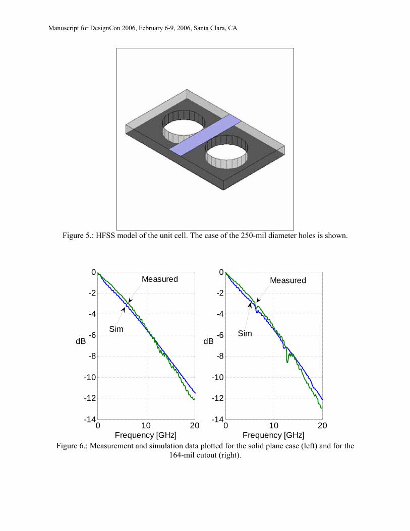
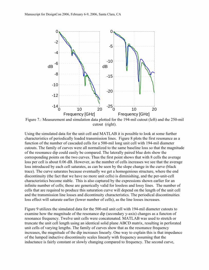
plane with 125-mil holes almost completely overlap. Measurment to Simulation Correlation HFSS [5], a full-wave 3-D field solver, was used to solve for the S-parameters of the test structure. Because the physical size of the test structure was large compared to the wavelengths involved and because the test structure exhibits a regular repeating pattern along the length of the microstrip, a unit cell approach was taken, where the test structure was divided into unit cells, each containing one pair of holes. Figure 5 shows a snapshot of the unit cell 3-D model. The unit cell was simulated, the unit cells were concatenated using MATLAB [6], and finally the S-parameters were obtained for the entire structure. Using this approach it was feasible to solve to a high-level of accuracy (delta S = 0.005) in a relatively short amount of time. Figure 6 shows the measurement and simulation data plotted for the solid plane case and the 164 mil hole. Figure 7 shows the same data plotted for the 194 and 250-mil holes. Good correlation is observed between measurement and simulation; the slope of the S12 curves is captured as well as the location of the first resonance. To more accurately capture the location of the first and second resonance, the frequency dependent dielectric properties of the test board substrate would need to be included in the simulations.
Manuscript for DesignCon 2006, February 6-9, 2006, Santa Clara, CA
Figure 5.: HFSS model of the unit cell. The case of the 250-mil diameter holes is shown.
0 10 20-14
-12
-10
-8
-6
-4
-2
0
Frequency [GHz]
dB
0 10 20-14
-12
-10
-8
-6
-4
-2
0
Frequency [GHz]
dB
Measured
Sim
Measured
Sim
Figure 6.: Measurement and simulation data plotted for the solid plane case (left) and for the
164-mil cutout (right).
Manuscript for DesignCon 2006, February 6-9, 2006, Santa Clara, CA
0 10 20-14
-12
-10
-8
-6
-4
-2
0
Frequency [GHz]
dB
0 10 20-25
-20
-15
-10
-5
0
Frequency [GHz]
dB
Figure 7.: Measurement and simulation data plotted for the 194-mil cutout (left) and the 250-mil
cutout (right).
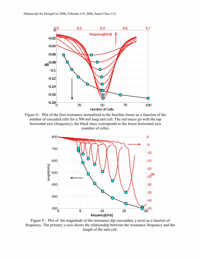
Using the simulated data for the unit cell and MATLAB it is possible to look at some further characteristics of periodically loaded transmission lines. Figure 8 plots the first resonance as a function of the number of cascaded cells for a 500-mil long unit cell with 194-mil diameter cutouts. The family of curves were all normalized to the same baseline loss so that the magnitude of the resonance dip could easily be compared. The laterally paired blue dots show the corresponding points on the two curves. Thus the first point shows that with 8 cells the average loss per cell is about 0.06 dB. However, as the number of cells increases we see that the average loss introduced by each cell saturates, as can be seen by the slope change in the curve (black trace). The curve saturates because eventually we get a homogenious structure, where the end discontinuity (the fact that we have no more unit cells) is diminishing, and the per-unit-cell characteristics become stable. This is also captured by the expressions shown earlier for an infinite number of cells; those are generically valid for lossless and lossy lines. The number of cells that are required to produce this saturation curve will depend on the length of the unit cell and the transmission line losses and dicontinuity characteristics. The periodical discontinuities loss effect will saturate earlier (lower number of cells), as the line losses increases. Figure 9 utilizes the simulated data for the 500-mil unit cell with 194-mil diameter cutouts to examine how the magnitude of the resonance dip (secondary y-axis) changes as a functon of resonance frequency. Twelve unit cells were concatenated. MATLAB was used to stretch or truncate the unit cell length using an identical solid plane ABCD matrix, resulting in perforated unit cells of varying lengths. The family of curves show that as the resonance frequency increases, the magnitude of the dip increases linearly. One way to explain this is that impedance of the lumped inductive discontinuity scales linearly with frequency assuming that the inductance is fairly constant or slowly changing compared to frequency. The second curve,
Manuscript for DesignCon 2006, February 6-9, 2006, Santa Clara, CA
0 25 50 75 100-0.18
-0.16
-0.14
-0.12
-0.1
-0.08
-0.06
-0.04
-0.02
0
Number of Cells
dB
5.9 6.1 6.3 6.5 6.7
-0.18
-0.16
-0.14
-0.12
-0.1
-0.08
-0.06
-0.04
-0.02
0frequency[GHz]
dB
Figure 8.: Plot of the first resonance normalized to the baseline losses as a function of the
number of cascaded cells for a 500-mil long unit cell. The red traces go with the top horizontal axis (frequency), the black trace corresponds to the lower horizontal axis
(number of cells).
0 5 10 15 20-45
-40
-35
-30
-25
-20
-15
-10
-5
0
frequency[GHz]
dB
0 5 10 15 20200
300
400
500
600
700
800
frequency[GHz]
leng
ht[m
ils]
Figure 9.: Plot of the magnitude of the resonance dip (secondary y-axis) as a functon of
frequency. The primary y-axis shows the relationship between the resonance frequency and the length of the unit cell.
Manuscript for DesignCon 2006, February 6-9, 2006, Santa Clara, CA
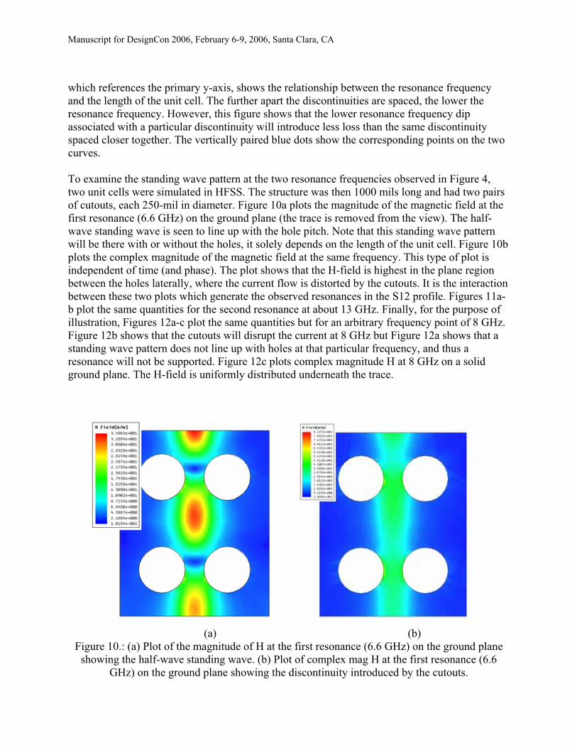
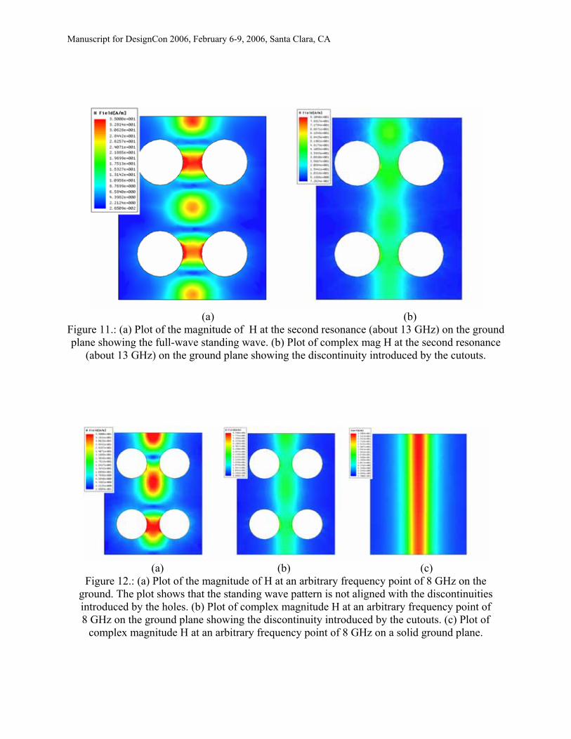
which references the primary y-axis, shows the relationship between the resonance frequency and the length of the unit cell. The further apart the discontinuities are spaced, the lower the resonance frequency. However, this figure shows that the lower resonance frequency dip associated with a particular discontinuity will introduce less loss than the same discontinuity spaced closer together. The vertically paired blue dots show the corresponding points on the two curves. To examine the standing wave pattern at the two resonance frequencies observed in Figure 4, two unit cells were simulated in HFSS. The structure was then 1000 mils long and had two pairs of cutouts, each 250-mil in diameter. Figure 10a plots the magnitude of the magnetic field at the first resonance (6.6 GHz) on the ground plane (the trace is removed from the view). The half-wave standing wave is seen to line up with the hole pitch. Note that this standing wave pattern will be there with or without the holes, it solely depends on the length of the unit cell. Figure 10b plots the complex magnitude of the magnetic field at the same frequency. This type of plot is independent of time (and phase). The plot shows that the H-field is highest in the plane region between the holes laterally, where the current flow is distorted by the cutouts. It is the interaction between these two plots which generate the observed resonances in the S12 profile. Figures 11a-b plot the same quantities for the second resonance at about 13 GHz. Finally, for the purpose of illustration, Figures 12a-c plot the same quantities but for an arbitrary frequency point of 8 GHz. Figure 12b shows that the cutouts will disrupt the current at 8 GHz but Figure 12a shows that a standing wave pattern does not line up with holes at that particular frequency, and thus a resonance will not be supported. Figure 12c plots complex magnitude H at 8 GHz on a solid ground plane. The H-field is uniformly distributed underneath the trace.
(a) (b)
Figure 10.: (a) Plot of the magnitude of H at the first resonance (6.6 GHz) on the ground plane showing the half-wave standing wave. (b) Plot of complex mag H at the first resonance (6.6
GHz) on the ground plane showing the discontinuity introduced by the cutouts.
Manuscript for DesignCon 2006, February 6-9, 2006, Santa Clara, CA
(a) (b) Figure 11.: (a) Plot of the magnitude of H at the second resonance (about 13 GHz) on the ground plane showing the full-wave standing wave. (b) Plot of complex mag H at the second resonance
(about 13 GHz) on the ground plane showing the discontinuity introduced by the cutouts.
(a) (b) (c)
Figure 12.: (a) Plot of the magnitude of H at an arbitrary frequency point of 8 GHz on the ground. The plot shows that the standing wave pattern is not aligned with the discontinuities introduced by the holes. (b) Plot of complex magnitude H at an arbitrary frequency point of 8 GHz on the ground plane showing the discontinuity introduced by the cutouts. (c) Plot of
complex magnitude H at an arbitrary frequency point of 8 GHz on a solid ground plane.
Manuscript for DesignCon 2006, February 6-9, 2006, Santa Clara, CA
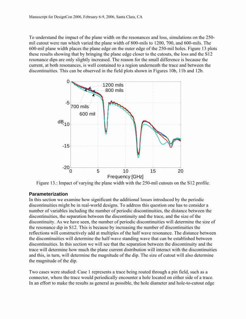
To understand the impact of the plane width on the resonances and loss, simulations on the 250-mil cutout were run which varied the plane width of 800-mils to 1200, 700, and 600-mils. The 600-mil plane width places the plane edge on the outer edge of the 250-mil holes. Figure 13 plots these results showing that by bringing the plane edge closer to the cutouts, the loss and the S12 resonance dips are only slightly increased. The reason for the small difference is because the current, at both resonances, is well contained to a region underneath the trace and between the discontinuities. This can be observed in the field plots shown in Figures 10b, 11b and 12b.
0 5 10 15 20-20
-15
-10
-5
0
Frequency [GHz]
dB
1200 mils800 mils
700 mils600 mil
Figure 13.: Impact of varying the plane width with the 250-mil cutouts on the S12 profile.
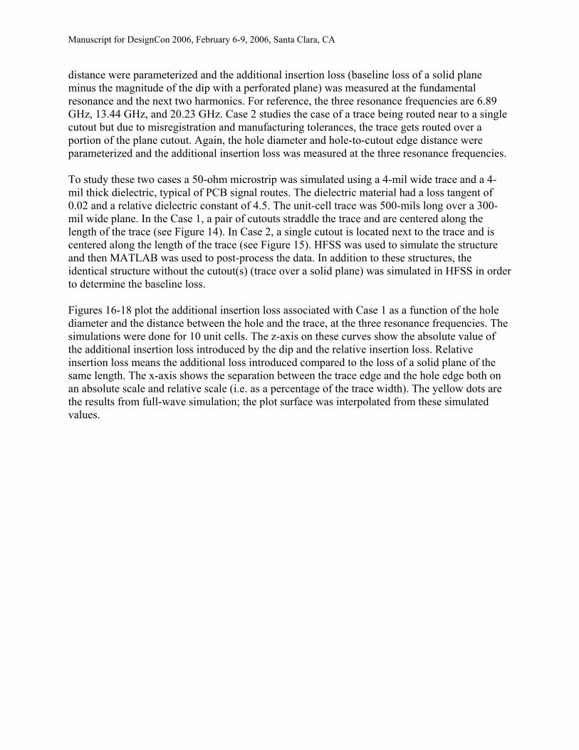
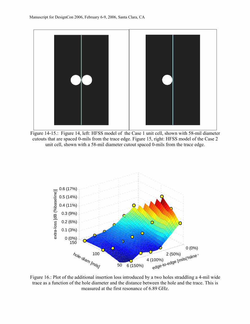
Parameterization In this section we examine how significant the additional losses introduced by the periodic discontinuities might be in real-world designs. To address this question one has to consider a number of variables including the number of periodic discontinuities, the distance between the discontinuities, the separation between the discontinuity and the trace, and the size of the discontinuity. As we have seen, the number of periodic discontinuities will determine the size of the resonance dip in S12. This is because by increasing the number of discontinuities the reflections will constructively add at multiples of the half wave resonance. The distance between the discontinuities will determine the half-wave standing wave that can be established between discontinuities. In this section we will see that the separation between the discontinuity and the trace will determine how much the plane current distribution will interact with the discontinuities and this, in turn, will determine the magnitude of the dip. The size of cutout will also determine the magnitude of the dip. Two cases were studied: Case 1 represents a trace being routed through a pin field, such as a connector, where the trace would periodically encounter a hole located on either side of a trace. In an effort to make the results as general as possible, the hole diameter and hole-to-cutout edge
Manuscript for DesignCon 2006, February 6-9, 2006, Santa Clara, CA
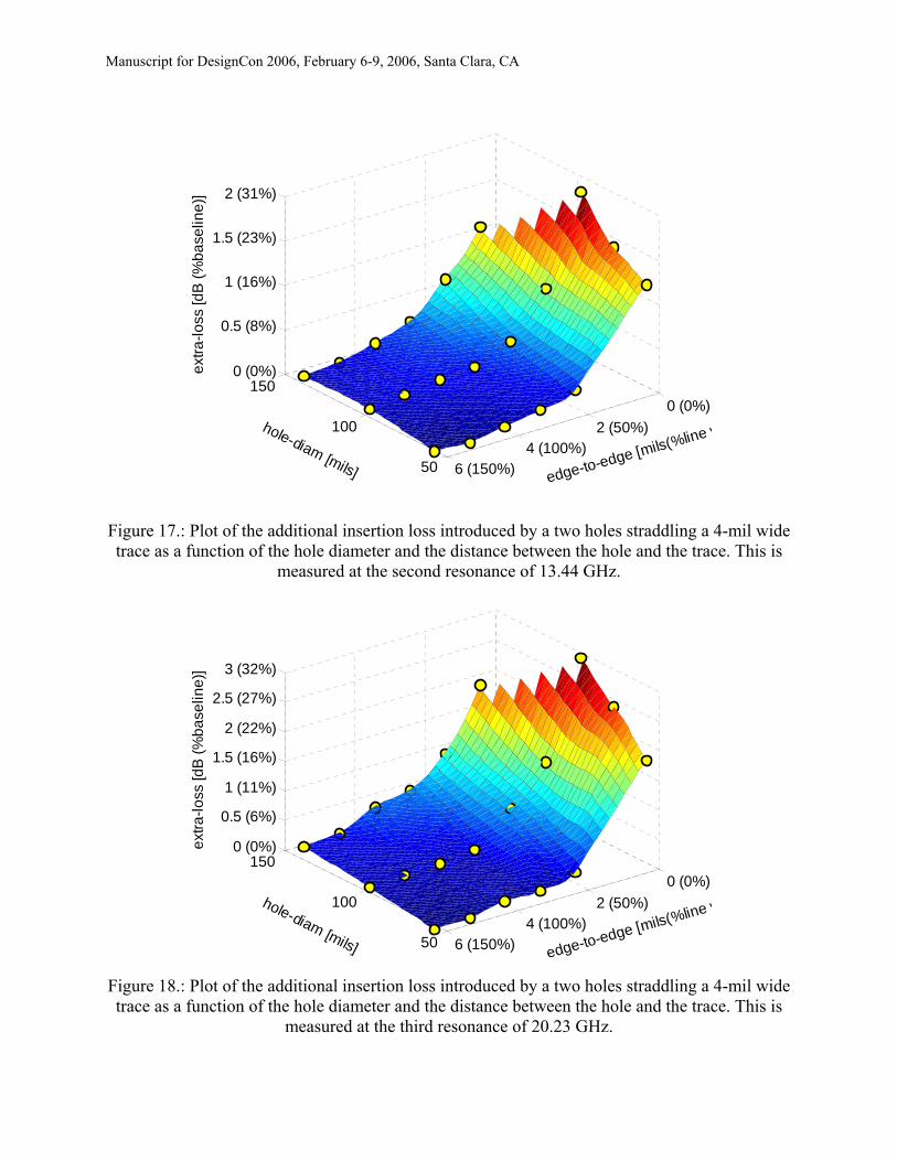
distance were parameterized and the additional insertion loss (baseline loss of a solid plane minus the magnitude of the dip with a perforated plane) was measured at the fundamental resonance and the next two harmonics. For reference, the three resonance frequencies are 6.89 GHz, 13.44 GHz, and 20.23 GHz. Case 2 studies the case of a trace being routed near to a single cutout but due to misregistration and manufacturing tolerances, the trace gets routed over a portion of the plane cutout. Again, the hole diameter and hole-to-cutout edge distance were parameterized and the additional insertion loss was measured at the three resonance frequencies. To study these two cases a 50-ohm microstrip was simulated using a 4-mil wide trace and a 4-mil thick dielectric, typical of PCB signal routes. The dielectric material had a loss tangent of 0.02 and a relative dielectric constant of 4.5. The unit-cell trace was 500-mils long over a 300-mil wide plane. In the Case 1, a pair of cutouts straddle the trace and are centered along the length of the trace (see Figure 14). In Case 2, a single cutout is located next to the trace and is centered along the length of the trace (see Figure 15). HFSS was used to simulate the structure and then MATLAB was used to post-process the data. In addition to these structures, the identical structure without the cutout(s) (trace over a solid plane) was simulated in HFSS in order to determine the baseline loss. Figures 16-18 plot the additional insertion loss associated with Case 1 as a function of the hole diameter and the distance between the hole and the trace, at the three resonance frequencies. The simulations were done for 10 unit cells. The z-axis on these curves show the absolute value of the additional insertion loss introduced by the dip and the relative insertion loss. Relative insertion loss means the additional loss introduced compared to the loss of a solid plane of the same length. The x-axis shows the separation between the trace edge and the hole edge both on an absolute scale and relative scale (i.e. as a percentage of the trace width). The yellow dots are the results from full-wave simulation; the plot surface was interpolated from these simulated values.
Manuscript for DesignCon 2006, February 6-9, 2006, Santa Clara, CA
Figure 14-15.: Figure 14, left: HFSS model of the Case 1 unit cell, shown with 58-mil diameter cutouts that are spaced 0-mils from the trace edge. Figure 15, right: HFSS model of the Case 2
unit cell, shown with a 58-mil diameter cutout spaced 0-mils from the trace edge.
0 (0%)2 (50%)
4 (100%)6 (150%)50
100
1500 (0%)
0.1 (3%)
0.2 (6%)
0.3 (9%)
0.4 (11%)
0.5 (14%)
0.6 (17%)
edge-to-edge [mils(%line whole-diam [mils]
extra
-loss
[dB
(%ba
selin
e)]
Figure 16.: Plot of the additional insertion loss introduced by a two holes straddling a 4-mil wide trace as a function of the hole diameter and the distance between the hole and the trace. This is
measured at the first resonance of 6.89 GHz.
Manuscript for DesignCon 2006, February 6-9, 2006, Santa Clara, CA
0 (0%)2 (50%)
4 (100%)6 (150%)50
100
1500 (0%)
0.5 (8%)
1 (16%)
1.5 (23%)
2 (31%)
edge-to-edge [mils(%line whole-diam [mils]
extra
-loss
[dB
(%ba
selin
e)]
Figure 17.: Plot of the additional insertion loss introduced by a two holes straddling a 4-mil wide trace as a function of the hole diameter and the distance between the hole and the trace. This is
measured at the second resonance of 13.44 GHz.
0 (0%)2 (50%)
4 (100%)6 (150%)50
100
1500 (0%)
0.5 (6%)
1 (11%)
1.5 (16%)
2 (22%)
2.5 (27%)
3 (32%)
edge-to-edge [mils(%line whole-diam [mils]
extra
-loss
[dB
(%ba
selin
e)]
Figure 18.: Plot of the additional insertion loss introduced by a two holes straddling a 4-mil wide trace as a function of the hole diameter and the distance between the hole and the trace. This is
measured at the third resonance of 20.23 GHz.
Manuscript for DesignCon 2006, February 6-9, 2006, Santa Clara, CA
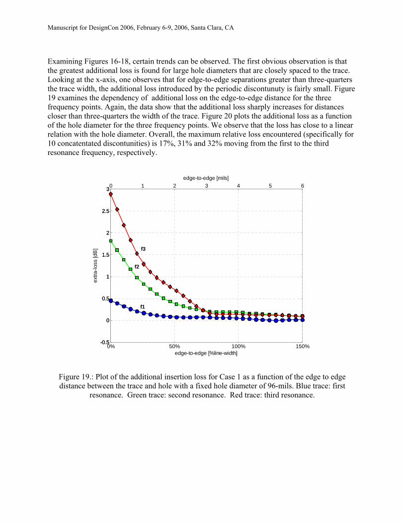
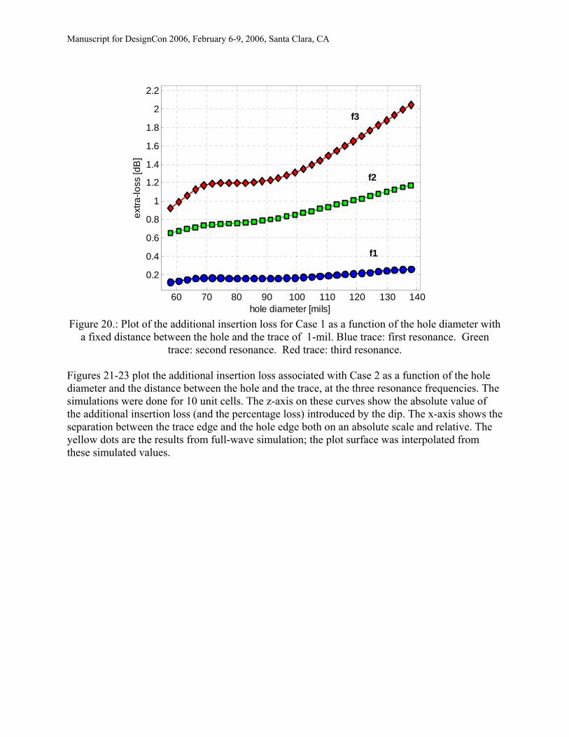
Examining Figures 16-18, certain trends can be observed. The first obvious observation is that the greatest additional loss is found for large hole diameters that are closely spaced to the trace. Looking at the x-axis, one observes that for edge-to-edge separations greater than three-quarters the trace width, the additional loss introduced by the periodic discontunuty is fairly small. Figure 19 examines the dependency of additional loss on the edge-to-edge distance for the three frequency points. Again, the data show that the additional loss sharply increases for distances closer than three-quarters the width of the trace. Figure 20 plots the additional loss as a function of the hole diameter for the three frequency points. We observe that the loss has close to a linear relation with the hole diameter. Overall, the maximum relative loss encountered (specifically for 10 concatentated discontunities) is 17%, 31% and 32% moving from the first to the third resonance frequency, respectively.
0% 50% 100% 150%-0.5
0
0.5
1
1.5
2
2.5
3
edge-to-edge [%line-width]
extra
-loss
[dB
]
0 1 2 3 4 5 6
-0.5
0
0.5
1
1.5
2
2.5
3
edge-to-edge [mils]
f3
f2
f1
Figure 19.: Plot of the additional insertion loss for Case 1 as a function of the edge to edge distance between the trace and hole with a fixed hole diameter of 96-mils. Blue trace: first
resonance. Green trace: second resonance. Red trace: third resonance.
Manuscript for DesignCon 2006, February 6-9, 2006, Santa Clara, CA
60 70 80 90 100 110 120 130 140
0.2
0.4
0.6
0.8
1
1.2
1.4
1.6
1.8
2
2.2
hole diameter [mils]
extra
-loss
[dB
]
f3
f2
f1
Figure 20.: Plot of the additional insertion loss for Case 1 as a function of the hole diameter with
a fixed distance between the hole and the trace of 1-mil. Blue trace: first resonance. Green trace: second resonance. Red trace: third resonance.
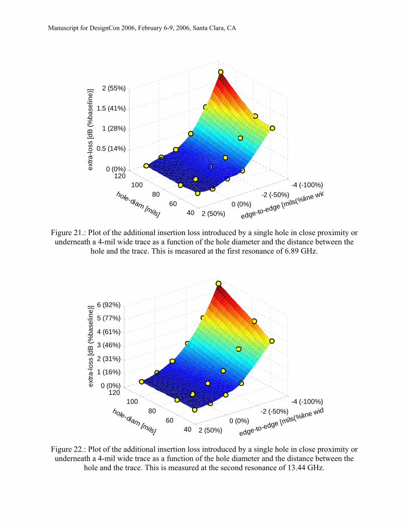
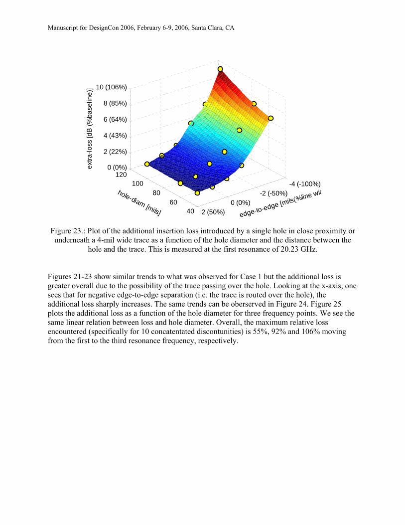
Figures 21-23 plot the additional insertion loss associated with Case 2 as a function of the hole diameter and the distance between the hole and the trace, at the three resonance frequencies. The simulations were done for 10 unit cells. The z-axis on these curves show the absolute value of the additional insertion loss (and the percentage loss) introduced by the dip. The x-axis shows the separation between the trace edge and the hole edge both on an absolute scale and relative. The yellow dots are the results from full-wave simulation; the plot surface was interpolated from these simulated values.
Manuscript for DesignCon 2006, February 6-9, 2006, Santa Clara, CA
-4 (-100%)-2 (-50%)
0 (0%)2 (50%)40
6080
100120
0 (0%)
0.5 (14%)
1 (28%)
1.5 (41%)
2 (55%)
edge-to-edge [mils(%line widhole-diam [mils]
extra
-loss
[dB
(%ba
selin
e)]
Figure 21.: Plot of the additional insertion loss introduced by a single hole in close proximity or underneath a 4-mil wide trace as a function of the hole diameter and the distance between the
hole and the trace. This is measured at the first resonance of 6.89 GHz.
-4 (-100%)-2 (-50%)
0 (0%)2 (50%)40
6080
100120
0 (0%)
1 (16%)
2 (31%)
3 (46%)
4 (61%)
5 (77%)
6 (92%)
edge-to-edge [mils(%line widthole-diam [mils]
extra
-loss
[dB
(%ba
selin
e)]
Figure 22.: Plot of the additional insertion loss introduced by a single hole in close proximity or underneath a 4-mil wide trace as a function of the hole diameter and the distance between the
hole and the trace. This is measured at the second resonance of 13.44 GHz.
Manuscript for DesignCon 2006, February 6-9, 2006, Santa Clara, CA
-4 (-100%)-2 (-50%)
0 (0%)2 (50%)40
6080
100120
0 (0%)
2 (22%)
4 (43%)
6 (64%)
8 (85%)
10 (106%)
edge-to-edge [mils(%line widhole-diam [mils]
extra
-loss
[dB
(%ba
selin
e)]
Figure 23.: Plot of the additional insertion loss introduced by a single hole in close proximity or underneath a 4-mil wide trace as a function of the hole diameter and the distance between the
hole and the trace. This is measured at the first resonance of 20.23 GHz.
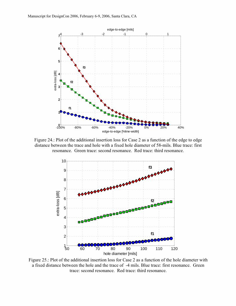
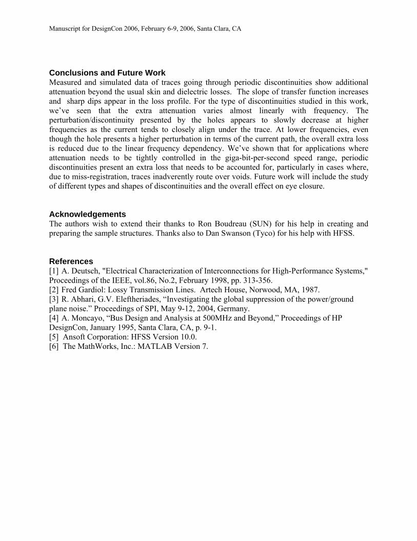
Figures 21-23 show similar trends to what was observed for Case 1 but the additional loss is greater overall due to the possibility of the trace passing over the hole. Looking at the x-axis, one sees that for negative edge-to-edge separation (i.e. the trace is routed over the hole), the additional loss sharply increases. The same trends can be oberserved in Figure 24. Figure 25 plots the additional loss as a function of the hole diameter for three frequency points. We see the same linear relation between loss and hole diameter. Overall, the maximum relative loss encountered (specifically for 10 concatentated discontunities) is 55%, 92% and 106% moving from the first to the third resonance frequency, respectively.
Manuscript for DesignCon 2006, February 6-9, 2006, Santa Clara, CA
-100% -80% -60% -40% -20% 0% 20% 40%0
1
2
3
4
5
6
7
edge-to-edge [%line-width]
extra
-loss
[dB
]
-4 -3 -2 -1 0 1
0
1
2
3
4
5
6
7
edge-to-edge [mils]
f3
f2
f1
Figure 24.: Plot of the additional insertion loss for Case 2 as a function of the edge to edge distance between the trace and hole with a fixed hole diameter of 58-mils. Blue trace: first
resonance. Green trace: second resonance. Red trace: third resonance.
50 60 70 80 90 100 110 1201
2
3
4
5
6
7
8
9
10
hole diameter [mils]
extra
-loss
[dB
]
f3
f2
f1
Figure 25.: Plot of the additional insertion loss for Case 2 as a function of the hole diameter with
a fixed distance between the hole and the trace of -4 mils. Blue trace: first resonance. Green trace: second resonance. Red trace: third resonance.
Manuscript for DesignCon 2006, February 6-9, 2006, Santa Clara, CA
Conclusions and Future Work Measured and simulated data of traces going through periodic discontinuities show additional attenuation beyond the usual skin and dielectric losses. The slope of transfer function increases and sharp dips appear in the loss profile. For the type of discontinuities studied in this work, we’ve seen that the extra attenuation varies almost linearly with frequency. The perturbation/discontinuity presented by the holes appears to slowly decrease at higher frequencies as the current tends to closely align under the trace. At lower frequencies, even though the hole presents a higher perturbation in terms of the current path, the overall extra loss is reduced due to the linear frequency dependency. We’ve shown that for applications where attenuation needs to be tightly controlled in the giga-bit-per-second speed range, periodic discontinuities present an extra loss that needs to be accounted for, particularly in cases where, due to miss-registration, traces inadverently route over voids. Future work will include the study of different types and shapes of discontinuities and the overall effect on eye closure. Acknowledgements The authors wish to extend their thanks to Ron Boudreau (SUN) for his help in creating and preparing the sample structures. Thanks also to Dan Swanson (Tyco) for his help with HFSS. References [1] A. Deutsch, "Electrical Characterization of Interconnections for High-Performance Systems," Proceedings of the IEEE, vol.86, No.2, February 1998, pp. 313-356. [2] Fred Gardiol: Lossy Transmission Lines. Artech House, Norwood, MA, 1987. [3] R. Abhari, G.V. Eleftheriades, “Investigating the global suppression of the power/ground plane noise.” Proceedings of SPI, May 9-12, 2004, Germany. [4] A. Moncayo, “Bus Design and Analysis at 500MHz and Beyond,” Proceedings of HP DesignCon, January 1995, Santa Clara, CA, p. 9-1. [5] Ansoft Corporation: HFSS Version 10.0. [6] The MathWorks, Inc.: MATLAB Version 7.