Embed Size (px)
Citation preview
20 times (13 dB) more power, even in a low power (QRP) contest. One more stage of amplification added to the 0.25 W amplifier can overcome that 13 dB difference. The 5 to 10 W output level is a common standard for portable radios with many commercially available examples.
Putting Power in the Antenna
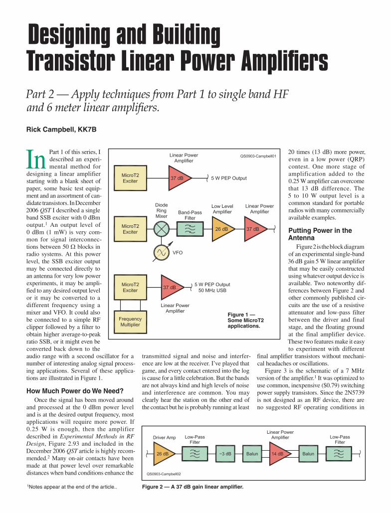
Figure 2 is the block diagram of an experimental single-band 36 dB gain 5 W linear amplifier that may be easily constructed using whatever output device is available. Two noteworthy dif-ferences between Figure 2 and other commonly published cir-cuits are the use of a resistive attenuator and low-pass filter between the driver and final stage, and the floating ground at the final amplifier device. These two features make it easy to experiment with different
final amplifier transistors without mechani-cal headaches or oscillations.
Figure 3 is the schematic of a 7 MHz version of the amplifier.1 It was optimized to use common, inexpensive ($0.79) switching power supply transistors. Since the 2N5739 is not designed as an RF device, there are no suggested RF operating conditions in
In Part 1 of this series, I described an experi-mental method for
designing a linear amplifier starting with a blank sheet of paper, some basic test equip-ment and an assortment of can-didate transistors. In December 2006 QST I described a single band SSB exciter with 0 dBm output.1 An output level of 0 dBm (1 mW) is very com-mon for signal interconnec-tions between 50 Ω blocks in radio systems. At this power level, the SSB exciter output may be connected directly to an antenna for very low power experiments, it may be ampli-fied to any desired output level or it may be converted to a different frequency using a mixer and VFO. It could also be connected to a simple RF clipper followed by a filter to obtain higher average-to-peak ratio SSB, or it might even be converted back down to the audio range with a second oscillator for a number of interesting analog signal process-ing applications. Several of these applica-tions are illustrated in Figure 1.
How Much Power do We Need?Once the signal has been moved around
and processed at the 0 dBm power level and is at the desired output frequency, most applications will require more power. If 0.25 W is enough, then the amplifier described in Experimental Methods in RF Design, Figure 2.93 and included in the December 2006 QST article is highly recom-mended.2 Many on-air contacts have been made at that power level over remarkable distances when band conditions enhance the
Designing and Building Transistor Linear Power AmplifiersPart 2 — Apply techniques from Part 1 to single band HF and 6 meter linear amplifiers.
Rick Campbell, KK7B
1Notes appear at the end of the article.. Figure 2 — A 37 dB gain linear amplifier.
Figure 1 — Some MicroT2 applications.
transmitted signal and noise and interfer-ence are low at the receiver. I’ve played that game, and every contact entered into the log is cause for a little celebration. But the bands are not always kind and high levels of noise and interference are common. You may clearly hear the station on the other end of the contact but he is probably running at least

the data sheet. The operating conditions were obtained experimentally by vary-ing the supply voltages while watching the output waveforms. The values of the π attenuators between stages were selected experimentally for best gain and distor-tion distribution among the three amplifier stages. The single-section low-pass filter on the output of the driver transistor made a sig-nificant reduction in high-order intermodu-lation products, and seemed to improve the symmetry of the intermodulation distortion products as well.
Tweaking it into SubmissionFigure 4 is the single-tone output spec-
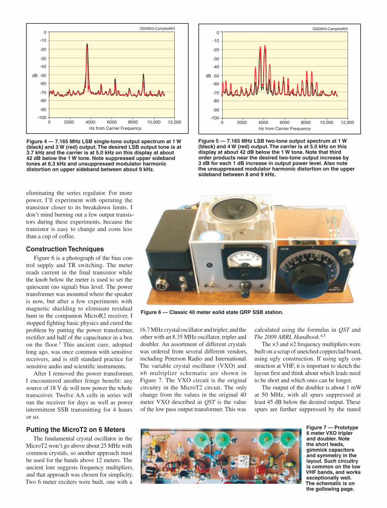
trum of the exciter driving the amplifier in Figure 3 with the two-tone output spectrum shown in Figure 5. Excellent linearity was obtained at a PEP output level of several watts.
Since the amplifier is experimental and the parts are inexpensive, I adjusted the col-lector supply voltage on the output stage up and down and observed the impact on AM and two-tone waveforms without wor-
rying much about burning out the device. I also varied the base bias, and changed the drive level with a step attenuator. As expected, increased collector voltage made a big improvement in the linearity of strong signals. Increased base bias improved the linearity of small signals.
Since 100% modulated AM, SSB and two-tone outputs vary from some peak volt-age all the way to zero, both collector supply voltage and base bias determine the linearity of the output. Each can also be used to destroy the device. Too much collector voltage will burn out the transistor directly (remember that the voltage at the collector will generally swing to significantly higher than twice the supply voltage, even in a linear amplifier). Too much base bias will either destroy the transistor quickly as it conducts too much collector current and overheats, or slowly as the base-emitter junction warms up and the device goes into thermal runaway. I enjoyed exploring these options in the design phase of this amplifier, but have not burned out a device since selecting the component values and supply voltages shown in Figure 3.
Give Me PowerThe collector power supply for the output
stage is a common circuit, with a big capaci-tor instead of the expected three terminal regulator. That gives me about 18 V open-circuit, and about 16 V at maximum output. The big capacitor is split in two. The little box on the floor holds 2200 µF while another 3500 µF is in the box with the speaker, vari-able bias supply, TR relay and 12 V three terminal regulator. The regulator supplies regulated voltage to the receiver, transmitter and other amplifier stages.
The big capacitor provides the low impedance at audio needed in a SSB linear amplifier. By splitting it in two all of the components in the power supply and regula-tor circuitry are physically and electrically close to a big reservoir capacitor. Keeping power supply lines clean is particularly important around receivers. It is a simple power supply for an inexpensive transistor, and any efficiency I would have gained by using an expensive 13.8 V linear RF power transistor in one of Granberg’s wonderfully engineered circuits is more than offset by
Figure 3 — 7 MHz linear amplifier based on inexpensive active devices.
calculated using the formulas in QST and The 2009 ARRL Handbook.4,5
The ×3 and ×2 frequency multipliers were built on a scrap of unetched copperclad board, using ugly construction. If using ugly con-struction at VHF, it is important to sketch the layout first and think about which leads need to be short and which ones can be longer.
The output of the doubler is about 1 mW at 50 MHz, with all spurs suppressed at least 45 dB below the desired output. These spurs are further suppressed by the tuned
eliminating the series regulator. For more power, I’ll experiment with operating the transistor closer to its breakdown limits. I don’t mind burning out a few output transis-tors during these experiments, because the transistor is easy to change and costs less than a cup of coffee.
Construction TechniquesFigure 6 is a photograph of the bias con-
trol supply and TR switching. The meter reads current in the final transistor while the knob below the meter is used to set the quiescent (no signal) bias level. The power transformer was mounted where the speaker is now, but after a few experiments with magnetic shielding to eliminate residual hum in the companion MicroR2 receiver, I stopped fighting basic physics and cured the problem by putting the power transformer, rectifier and half of the capacitance in a box on the floor.3 This ancient cure, adopted long ago, was once common with sensitive receivers, and is still standard practice for sensitive audio and scientific instruments.
After I removed the power transformer, I encountered another fringe benefit: any source of 18 V dc will now power the whole transceiver. Twelve AA cells in series will run the receiver for days as well as power intermittent SSB transmitting for 4 hours or so.
Putting the MicroT2 on 6 MetersThe fundamental crystal oscillator in the
MicroT2 won’t go above about 25 MHz with common crystals, so another approach must be used for the bands above 12 meters. The ancient lore suggests frequency multipliers, and that approach was chosen for simplicity. Two 6 meter exciters were built, one with a
16.7 MHz crystal oscillator and tripler, and the other with an 8.35 MHz oscillator, tripler and doubler. An assortment of different crystals was ordered from several different vendors, including Peterson Radio and International. The variable crystal oscillator (VXO) and ×6 multiplier schematic are shown in Figure 7. The VXO circuit is the original circuitry in the MicroT2 circuit. The only change from the values in the original 40 meter VXO described in QST is the value of the low pass output transformer. This was
Figure 4 — 7.165 MHz LSB single-tone output spectrum at 1 W (black) and 3 W (red) output. The desired LSB output tone is at 3.7 kHz and the carrier is at 5.0 kHz on this display at about 42 dB below the 1 W tone. Note suppressed upper sideband tones at 6.3 kHz and unsuppressed modulator harmonic distortion on upper sideband between about 9 kHz.
Figure 5 — 7.165 MHz LSB two-tone output spectrum at 1 W (black) and 4 W (red) output. The carrier is at 5.0 kHz on this display at about 42 dB below the 1 W tone. Note that third order products near the desired two-tone output increase by 3 dB for each 1 dB increase in output power level. Also note the unsuppressed modulator harmonic distortion on the upper sideband between 8 and 9 kHz.
Figure 6 — Classic 40 meter solid state QRP SSB station.
Figure 7 — Prototype 6 meter VXO tripler and doubler. Note the short leads, gimmick capacitors and symmetry in the layout. Such circuitry is common on the low VHF bands, and works exceptionally well. The schematic is on the gollowing page.
12,00010,00080006000400020000
0
-10
-20
-30
-40
-50dB
-60
-70
-80
-90
-100
QS0903-Campbell04
Hz from Carrier Frequency12,00010,00080006000
Hz from Carrier Frequency400020000
0
-10
-20
-30
-40
-50dB
-60
-70
-80
-90
-100
QS0903-Campbell05

Prototype version with VXO on same PC board. There are some minor circuit differences.
Rick Campbell KK7BNovember 2007
scraps left on bench
Prototype version with VXO on same PC board. There are some minor circuit differences.
Rick Campbell KK7BNovember 2007
scraps left on bench

Figure 8 — Schematic of 6 meter amplifier.
Figure 9 — Photograph of the 6 meter 5 W SSB transmitter. The MicroT2 with ×6 exciter is in the black diecast box in the lower right. The VXO knob is in the middle, and the MIC connector on the right. The crystal socket on the front panel is a mistake — the crystal belongs inside the box where it is thermally and electrically shielded.
RF amplifier in the MicroT2, and by the narrow-band interstage tuning networks in the linear amplifier. The tuned doubler output drives the original MicroT2 buffer amplifier circuit. The only other change to the MicroT2 is retuning the RF ampli-fier output to 50 MHz. That may be easily done by changing MicroT2 L3 to 16 turns on a T25-6 ferrite toroid, changing C21 to a 20 pF trimmer, and leaving C20 out of the circuit. If the MicroT2 RF amplifier stage is built using ugly construction, short leads are necessary, particularly for connections to the gate of Q6.
Experiments with running the TUF-3 mixers as third harmonic mixers with direct IQ LO drive at 16.7 MHz were initially encouraging, with very good carrier sup-pression at 50 MHz, but distortion was high. A very simple rig could be built with that approach.
The 8 MHz crystal from International in the large can provides a very stable fre-quency tuning range of about 50 kHz on 6 meters, over the useful range from 50.115 to 50.165 MHz. The 16.7 MHz crys-tal and tripler provides a narrower range,
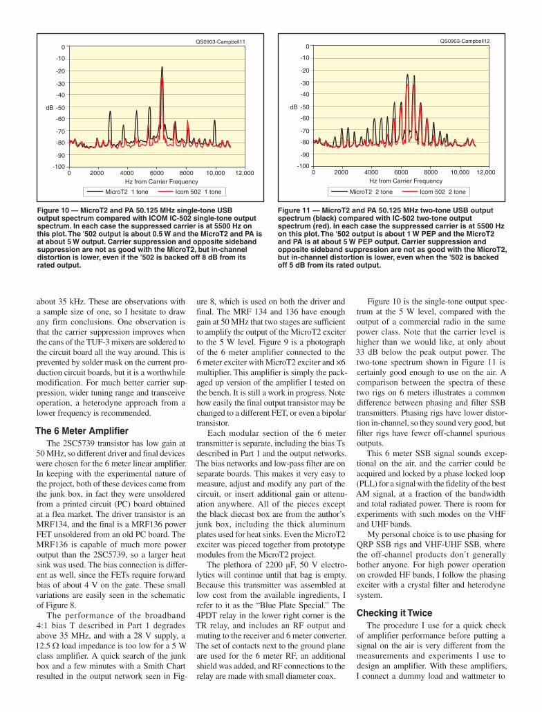
Figure 10 — MicroT2 and PA 50.125 MHz single-tone USB output spectrum compared with ICOM IC-502 single-tone output spectrum. In each case the suppressed carrier is at 5500 Hz on this plot. The '502 output is about 0.5 W and the MicroT2 and PA is at about 5 W output. Carrier suppression and opposite sideband suppression are not as good with the MicroT2, but in-channel distortion is lower, even if the ’502 is backed off 8 dB from its rated output.
Figure 11 — MicroT2 and PA 50.125 MHz two-tone USB output spectrum (black) compared with IC-502 two-tone output spectrum (red). In each case the suppressed carrier is at 5500 Hz on this plot. The '502 output is about 1 W PEP and the MicroT2 and PA is at about 5 W PEP output. Carrier suppression and opposite sideband suppression are not as good with the MicroT2, but in-channel distortion is lower, even when the '502 is backed off 5 dB from its rated output.
about 35 kHz. These are observations with a sample size of one, so I hesitate to draw any firm conclusions. One observation is that the carrier suppression improves when the cans of the TUF-3 mixers are soldered to the circuit board all the way around. This is prevented by solder mask on the current pro-duction circuit boards, but it is a worthwhile modification. For much better carrier sup-pression, wider tuning range and transceive operation, a heterodyne approach from a lower frequency is recommended.
The 6 Meter AmplifierThe 2SC5739 transistor has low gain at
50 MHz, so different driver and final devices were chosen for the 6 meter linear amplifier. In keeping with the experimental nature of the project, both of these devices came from the junk box, in fact they were unsoldered from a printed circuit (PC) board obtained at a flea market. The driver transistor is an MRF134, and the final is a MRF136 power FET unsoldered from an old PC board. The MRF136 is capable of much more power output than the 2SC5739, so a larger heat sink was used. The bias connection is differ-ent as well, since the FETs require forward bias of about 4 V on the gate. These small variations are easily seen in the schematic of Figure 8.
The performance of the broadband 4:1 bias T described in Part 1 degrades above 35 MHz, and with a 28 V supply, a 12.5 Ω load impedance is too low for a 5 W class amplifier. A quick search of the junk box and a few minutes with a Smith Chart resulted in the output network seen in Fig-
ure 8, which is used on both the driver and final. The MRF 134 and 136 have enough gain at 50 MHz that two stages are sufficient to amplify the output of the MicroT2 exciter to the 5 W level. Figure 9 is a photograph of the 6 meter amplifier connected to the 6 meter exciter with MicroT2 exciter and ×6 multiplier. This amplifier is simply the pack-aged up version of the amplifier I tested on the bench. It is still a work in progress. Note how easily the final output transistor may be changed to a different FET, or even a bipolar transistor.
Each modular section of the 6 meter transmitter is separate, including the bias Ts described in Part 1 and the output networks. The bias networks and low-pass filter are on separate boards. This makes it very easy to measure, adjust and modify any part of the circuit, or insert additional gain or attenu-ation anywhere. All of the pieces except the black diecast box are from the author’s junk box, including the thick aluminum plates used for heat sinks. Even the MicroT2 exciter was pieced together from prototype modules from the MicroT2 project.
The plethora of 2200 µF, 50 V electro-lytics will continue until that bag is empty. Because this transmitter was assembled at low cost from the available ingredients, I refer to it as the “Blue Plate Special.” The 4PDT relay in the lower right corner is the TR relay, and includes an RF output and muting to the receiver and 6 meter converter. The set of contacts next to the ground plane are used for the 6 meter RF, an additional shield was added, and RF connections to the relay are made with small diameter coax.
Figure 10 is the single-tone output spec-trum at the 5 W level, compared with the output of a commercial radio in the same power class. Note that the carrier level is higher than we would like, at only about 33 dB below the peak output power. The two-tone spectrum shown in Figure 11 is certainly good enough to use on the air. A comparison between the spectra of these two rigs on 6 meters illustrates a common difference between phasing and filter SSB transmitters. Phasing rigs have lower distor-tion in-channel, so they sound very good, but filter rigs have fewer off-channel spurious outputs.
This 6 meter SSB signal sounds excep-tional on the air, and the carrier could be acquired and locked by a phase locked loop (PLL) for a signal with the fidelity of the best AM signal, at a fraction of the bandwidth and total radiated power. There is room for experiments with such modes on the VHF and UHF bands.
My personal choice is to use phasing for QRP SSB rigs and VHF-UHF SSB, where the off-channel products don’t generally bother anyone. For high power operation on crowded HF bands, I follow the phasing exciter with a crystal filter and heterodyne system.
Checking it TwiceThe procedure I use for a quick check
of amplifier performance before putting a signal on the air is very different from the measurements and experiments I use to design an amplifier. With these amplifiers, I connect a dummy load and wattmeter to
12,00010,00080006000400020000
0
-10
-20
-30
-40
-50dB
-60
-70
-80
-90
-100
QS0903-Campbell11
MicroT2 1 tone Icom 502 1 tone
Hz from Carrier Frequency
12,00010,00080006000400020000
0
-10
-20
-30
-40
-50dB
-60
-70
-80
-90
-100
QS0903-Campbell12
MicroT2 2 tone Icom 502 2 tone
Hz from Carrier Frequency

the output of the low-pass filter, and drive the amplifier chain to saturation with a CW signal. I observe the current drain at this saturated output level, and then set the rest-ing bias to about one tenth that level. These 5 W amplifiers idle at around 100 mA, so that is 1.8 W for the 7 MHz amplifier and 2.7 W for the 6 meter version. Then I speak into the microphone and observe that the output peaks are about 3 dB below the satu-rated CW output level. That results in a very nice sounding signal on the air.
If you have been doing the math, you can quickly estimate that my average output power on SSB ends up being about one tenth the saturated CW output power. PEP output capability is considerably higher than the average, but I prefer natural sounding SSB to the highly processed sound that results in an average power output very close to the PEP output capability of the amplifier. This is personal preference, and directly related to my willingness to switch to CW when sig-nals are marginal. CW is no longer a require-
ment, it’s a choice, and in many cases it will get through when nothing else will. SSB is nice for casual conversations, digital modes are wonderful if you don’t mind sharing the fun with a computer, but CW is simple and the power advantage on transmit is only part of the equation.
The linear amplifiers described in this article are remarkable in two ways: The experimental design procedure
provides a real education in linear ampli-fier design, measurement, adjustment and construction. They were designed around the devices
on hand, and built at nearly zero cost.In that sense, they follow the best tradi-
tions of the Amateur Radio service and inno-vative design engineering.
Notes1R. Campbell, KK7B, “The MicroT2 — A
Compact Single-Band SSB Transmitter,” QST, Dec 2006, pp 28-33.
2W. Hayward, W7ZOI, R. Campbell, KK7B, and B. Larkin, W7PUA, Experimental Methods in RF Design. Available from your ARRL dealer
or the ARRL Bookstore, ARRL order no. 8799. Telephone 860-594-0355, or toll-free in the US 888-277-5289; www.arrl.org/shop; [email protected].
3R. Campbell, KK7B, “The MicroR2 — An Easy to Build ‘Single Signal’ SSB or CW Receiver,” QST, Oct 2006, pp 28-33.
4The ARRL Handbook for Radio Communica-tions, 2009 Edition. Available from your ARRL dealer or the ARRL Bookstore, ARRL order no. 0261 (Hardcover 0292). Telephone 860-594-0355, or toll-free in the US 888-277-5289; www.arrl.org/shop; [email protected].
5This circuitry is nearly identical to the circuit used for the 40 meter version, and can use the same circuit traces. The output may be taken from MicroT2 C41 by leaving R59, 60 and 61 off the circuit board. The VHF ugly constructed tripler and doubler circuitry is inserted in the MicroT2 circuit in place of R60. Short small diameter coax or twisted pair should be used for the interconnections. This circuitry should be shielded from the RF output amplifier to improve carrier sup-pression.
See Part 1 for Rick’s biography. You can con-tact Rick at 4105 NW Carlton Ct, Portland, OR 97229, or at [email protected].