Embed Size (px)
Citation preview
Maxim > Design Support > Technical Documents > Application Notes > Power-Supply Circuits > APP 5504
Keywords: flyback, continuous conduction mode, CCM, discontinuous conduction mode, DCM,transformer, optoisolated feedback, error amplifier compensation, pi controller, biasing optocoupler,flyback converter, peak current mode controller, MAX17596, MAX17595
APPLICATION NOTE 5504
Designing Flyback Converters Using Peak-Current-Mode ControllersBy: Srinivasa Rao MeesalaNov 27, 2012
Abstract: Flyback converter design using MAX17595/MAX17596 is outlined. Design methodology andcalculations for components value selection are presented. Continuous conduction mode (CCM) anddiscontinuous conduction mode (DCM) are treated individually.
IntroductionThis application note describes the methodology of designing flyback converters using theMAX17595/MAX17596 peak-current-mode controllers. Flyback converters may be operated indiscontinuous conduction mode (DCM) or continuous conduction mode (CCM). The component choices,stress level in power devices, and controller design vary depending on the operating mode of theconverter. Formulas for calculating component values and ratings are also presented.
DCM FlybackPrimary Inductance SelectionIn a DCM flyback converter, the energy stored in the primary inductance of the flyback transformer isdelivered entirely to the output. The maximum primary-inductance value for which the converter remainsin DCM at all operating conditions can be calculated as:
(Eq. 1)
Where DMAX is chosen as 0.43 for the MAX17595/MAX17596, VD is the voltage drop of the outputrectifier diode on the secondary winding, and FSW is the switching frequency of the power converter.Choose the primary inductance value to be less than LPRIMAX.
Duty Cycle CalculationThe accurate value of the duty cycle (DNEW) for the selected primary inductance (LPRI) can be
Page 1 of 23
calculated using the following equation:
(Eq. 2)
Turns Ratio Calculation (NS/NP)Transformer turns ratio (K = NS/NP) can be calculated as:
(Eq. 3)
Peak/RMS Current CalculationPrimary and secondary RMS currents and primary peak current calculations are needed to design thetransformer in switched-mode power supplies. Also, primary peak current is used in setting the currentlimit. Use the following equations to calculate the primary and secondary peak and RMS currents.
Maximum primary peak current, (Eq. 4)
Maximum primary RMS current, (Eq. 5)
Maximum secondary peak current, (Eq. 6)
Maximum secondary RMS current, (Eq. 7)
For the purpose of current limit setting, the peak current may be calculated as follows:
ILIM = IPRIPEAK × 1.2 (Eq. 8)
Primary Snubber SelectionIdeally, the external MOSFET experiences a drain-source voltage stress equal to the sum of the inputvoltage and reflected voltage across the primary winding during the OFF period of the MOSFET. Inpractice, parasitic inductors and capacitors in the circuit, such as leakage inductance of the flybacktransformer, cause voltage overshoot and ringing in addition to the ideally expected voltage stress.Snubber circuits are used to limit the voltage overshoots to safe levels within the voltage rating of theexternal MOSFET. The snubber capacitor can be calculated using the following equation:
(Eq. 9)
Page 2 of 23
Where LLK is the leakage inductance that can be obtained from the transformer specifications (usually1% to 2% of the primary inductance).
The power that must be dissipated in the snubber resistor is calculated using the following formula:
PSNUB = 0.833 × LLK × IPRIPEAK² × FSW (Eq. 10)
The snubber resistor is calculated based on the equation below:
(Eq. 11)
The voltage rating of the snubber diode is:
VDSNUB = VINMAX + (2.5 × VOUT/K) (Eq. 12)
Output Capacitor SelectionX7R ceramic output capacitors are preferred in industrial applications due to their stability overtemperature. The output capacitor is usually sized to support a step load of 50% of the rated outputcurrent in nonisolated applications so that the output voltage deviation is contained to 3% of the ratedoutput voltage. The output capacitance can be calculated as follows:
(Eq. 13)
(Eq. 14)
The output capacitor RMS current rating can be calculated as follows:
(Eq. 15)
Where ISTEP is the load step, TRESPONSE is the response time of the controller, ΔVOUT is the allowableoutput voltage deviation, and FC is the target closed-loop crossover frequency. FC is chosen to be 1/10of the switching frequency FSW. For the flyback converter, the output capacitor supplies the load currentwhen the main switch is on, and therefore the output voltage ripple is a function of load current and dutycycle. Use the following equation to calculate the output capacitor ripple:
(Eq. 16)
Where IOUT is load current and DNEW is the duty cycle at minimum input voltage.
Page 3 of 23
Input Capacitor SelectionThe MAX17595 is optimized to implement offline AC-DC converters. In such applications, the inputcapacitor must be selected based on either the ripple due to the rectified line voltage, or based onholdup-time requirements. Holdup time can be defined as the time period over which the power supplyshould regulate its output voltage from the instant the AC power fails. The MAX17596 is useful inimplementing low-voltage DC-DC applications where the switching-frequency ripple must be used tocalculate the input capacitor. In both cases, the capacitor must be sized to meet RMS currentrequirements for reliable operation.
Capacitor Selection Based on Switching Ripple (MAX17596)For DC-DC applications, X7R ceramic capacitors are recommended due to their stability over theoperating temperature range. The effective series resistance (ESR) and effective series inductance (ESL)of a ceramic capacitor are relatively low, so the ripple voltage is dominated by the capacitive component.For the flyback converter, the input capacitor supplies the current when the main switch is on. Use thefollowing equation to calculate the input capacitor for a specified peak-to-peak input switching ripple(VIN_RIP):
(Eq. 17)
The input capacitor RMS current in low-voltage DC-DC applications can be calculated as follows:
(Eq. 18)
Capacitor Selection Based on Rectified Line Voltage Ripple (MAX17595)For the flyback converter, the input capacitor supplies the input current when the diode rectifier is off.The voltage discharge on the input capacitor, due to the input average current, should be within thelimits specified.
Assuming 25% ripple present on input DC capacitor, the input capacitor can be calculated as follows:
(Eq. 19)
WherePLOAD = rated output powerη = typical efficiency at VAC,MIN and ILOADVIN,PK = √2 × VAC,MIN = peak voltage at minimum input AC voltage.
Capacitor Selection Based on Holdup Time Requirements (MAX17595)For a given output power (PHOLDUP) that needs to be delivered during holdup time (THOLDUP), the DCbus voltage at which the AC supply fails (VINFAIL), and the minimum DC bus voltage at which theconverter can regulate the output voltages (VINMIN), the input capacitor (CIN) is estimated as:
Page 4 of 23
(Eq. 20)
The input capacitor RMS current for AC-DC applications can be calculated as:
(Eq. 21)
External MOSFET SelectionMOSFET selection criteria include maximum drain voltage, peak/RMS current in the primary, and themaximum allowable power dissipation of the package without exceeding the junction temperature limits.The voltage seen by the MOSFET drain is the sum of the input voltage, the reflected secondary voltageon the transformer primary, and the leakage inductance spike. The MOSFET’s absolute maximum VDSrating must be higher than the worst-case drain voltage:
(Eq. 22)
The drain current rating of the external MOSFET is selected to be greater than the worst-case peakcurrent limit setting.
Secondary Diode SelectionSecondary-diode-selection criteria includes the maximum reverse voltage, average current in thesecondary, reverse recovery time, junction capacitance, and the maximum allowable power dissipation ofthe package. The voltage stress on the diode is the sum of the output voltage and the reflected primaryvoltage. The maximum operating reverse-voltage rating must be higher than the worst-case reversevoltage:
VSECDIODE = 1.25 × (K × VINMAX + VOUT) (Eq. 23)
The current rating of the secondary diode should be selected so that the power loss in the diode (givenas the product of forward-voltage drop and the average diode current) should be low enough to ensurethat the junction temperature is within limits. Select fast-recovery diodes with a recovery time less than50ns, or Schottky diodes with low junction capacitance.
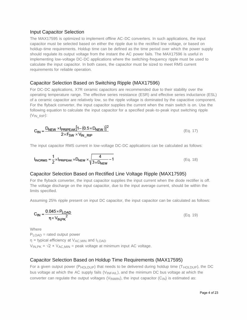
Error Amplifier Compensation DesignFor nonisolated designs, output voltage feedback and the loop compensation network are connected asshown in Figure 1.
Page 5 of 23
Figure 1. Loop compensation arrangement for nonisolated designs.
The loop compensation values are calculated as:
(Eq. 24)
Where:
(Eq. 25)
FSW is the switching frequency.
CCM FlybackTransformer Turns Ratio Calculation (K = NS/NP)The transformer turns ratio can be calculated using the following formula:
(Eq. 26)
Where DMAX is the duty cycle assumed at minimum input (0.43 for the MAX17595/MAX17596).
Page 6 of 23
Primary Inductance CalculationCalculate the primary inductance based on the ripple:
(Eq. 27)
Where DNOM, the nominal duty cycle at nominal operating DC input voltage VINNOM, is given as:
(Eq. 28)
The output current, down to which the flyback converter should operate in CCM, is determined byselection of β in Equation 27. For example, β should be selected as 0.15 so that the converter operatesin CCM down to 15% of the maxim output load current. The ripple in the primary current waveform is afunction of the duty cycle; maximum ripple occurs at the maximum DC input voltage. Therefore, themaximum (worst-case) load current down to which the converter operates in CCM occurs at themaximum operating DC input voltage. VD is the forward drop of the selected output diode at maximumoutput current.
Peak and RMS Current CalculationPrimary and secondary RMS currents and primary peak current calculations are needed to design thetransformer in switched-mode power supplies. Also, primary peak current is used in setting the currentlimit. Use the following equations to calculate the primary and secondary peak and RMS currents.
Maximum primary peak current:
(Eq. 29)
Maximum primary RMS current:
(Eq. 30)
Where ΔIPRI is the ripple current in the primary current waveform, and is given by:
(Eq. 31)
Maximum secondary peak current:
ISECPEAK = IPRIPEAK/K (Eq. 32)
Maximum secondary RMS current:
Page 7 of 23
(Eq. 33)
Where ΔISEC is the ripple current in the secondary current waveform, and is given by:
(Eq. 34)
For the purpose of current-limit setting, the peak current can be calculated as follows:
ILIM = IPRIPEAK × 1.2 (Eq. 35)
Primary RCD Snubber SelectionThe design procedure for primary RCD snubber selection is identical to that outlined in the DCM Flybacksection.
Output Capacitor SelectionX7R ceramic output capacitors are preferred in industrial applications due to their stability overtemperature. The output capacitor is usually sized to support a step load of 50% of the rated outputcurrent in nonisolated applications so that the output-voltage deviation is contained to 3% of the ratedoutput voltage. The output capacitance can be calculated as:
(Eq. 36)
(Eq. 37)
The output capacitor RMS current rating can be calculated as follows:
(Eq. 38)
Where ISTEP is the load step, TRESPONSE is the response time of the controller, ΔVOUT is the allowableoutput voltage deviation, and FC is the target closed-loop crossover frequency. FC is chosen to be lessthan 1/5 of the worst-case (lowest) RHP zero frequency FRHP. The right half-plane zero frequency iscalculated as follows:
(Eq. 39)
For the CCM flyback converter, the output capacitor supplies the load current when the main switch ison, and therefore, the output-voltage ripple is a function of load current and duty cycle. Use Equation 40
Page 8 of 23
to estimate the output-voltage ripple:
(Eq. 40)
Input Capacitor Selection (MAX17596)Use Equation 41 to calculate the input capacitor for a specified peak-to-peak input switching ripple(VIN_RIP) in low-voltage DC-DC converters operating in CCM mode.
(Eq. 41)
(Eq. 42)
Error Amplifier Compensation DesignFor nonisolated designs, the output voltage feedback and loop compensation network are connected asshown in Figure 1.
In the CCM flyback converter, the primary inductance and the equivalent load resistance introduces aright half-plane zero at the following frequency:
(Eq. 43)
The loop compensation values are calculated as:
(Eq. 44)
Where FP, the pole due to output capacitor and load, is given by:
(Eq. 45)
The above selection of RZ sets the loop-gain crossover frequency (FC, where the loop gain equals 1)equal to 1/5 the right-half plane zero frequency.
FC ≤ FZRHP/5
With the control loop zero placed at the load pole frequency:
(Eq. 46)
Page 9 of 23
With the high-frequency pole placed at half the switching frequency:
(Eq. 47)
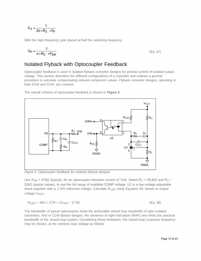
Isolated Flyback with Optocoupler FeedbackOptocoupler feedback is used in isolated flyback converter designs for precise control of isolated outputvoltage. This section describes the different configurations of a controller and outlines a generalprocedure to calculate compensating network component values. Flyback converter designs, operating inboth DCM and CCM, are covered.
The overall scheme of optocoupler feedback is shown in Figure 2.
Figure 2. Optocoupler feedback for isolated flyback designs.
Use RFB = 470Ω (typical), for an optocoupler transistor current of 1mA. Select R1 = 49.9kΩ and R2 =22kΩ (typical values), to use the full range of available COMP voltage. U3 is a low-voltage adjustableshunt regulator with a 1.24V reference voltage. Calculate RLED using Equation 48, based on outputvoltage VOUT.
RLED = 400 × CTR × (VOUT - 2.7)Ω (Eq. 48)
The bandwidth of typical optocouplers limits the achievable closed loop bandwidth of opto-isolatedconverters. And in CCM flyback designs, the presence of right-half-plane (RHP) zero limits the practicalbandwidth of the closed-loop system. Considering these limitations, the closed-loop crossover frequencymay be chosen, at the nominal input voltage as follows:
Page 10 of 23
ƒC = 5kHz, for DCM designs (Eq. 49)
Or ƒC = ƒZRHP/10, for CCM designs, limited to ƒC = 5kHz (Eq. 50)
Closed-loop compensation values are designed based on the open-loop gain at the desired crossoverfrequency, ƒC. The open-loop gains in DCM and CCM, at ƒC, are calculated using the followingexpressions.
Or ƒC = ƒZRHP/10, for CCM designs, limited to ƒC = 5kHz (Eq. 50)
, for DCM designs (Eq. 51)
And
, for
CCM designs
(Eq. 52)
WhereK = NS/NP is the transformer turns ratioƒP = IOUT/(π × VOUT × COUT), for DCM designs
And
, for CCM designs
Three controller configurations are suggested, based on open-loop gain and the value of RLED. Fortypical designs, the current transfer ratio (CTR) of the optocoupler designs can be assumed to be unity.It is known that the comparator and gate driver delays associated with the input voltage variations affectsthe optocoupler CTR. Depending on the optocopler selected, variations in CTR causes wide variations inbandwidth of the closed-loop system across the input-voltage operating range. It is recommended toselect an optocoupler with less CTR variations across the operating range.
Configuration1:
(Eq. 53)
Page 11 of 23
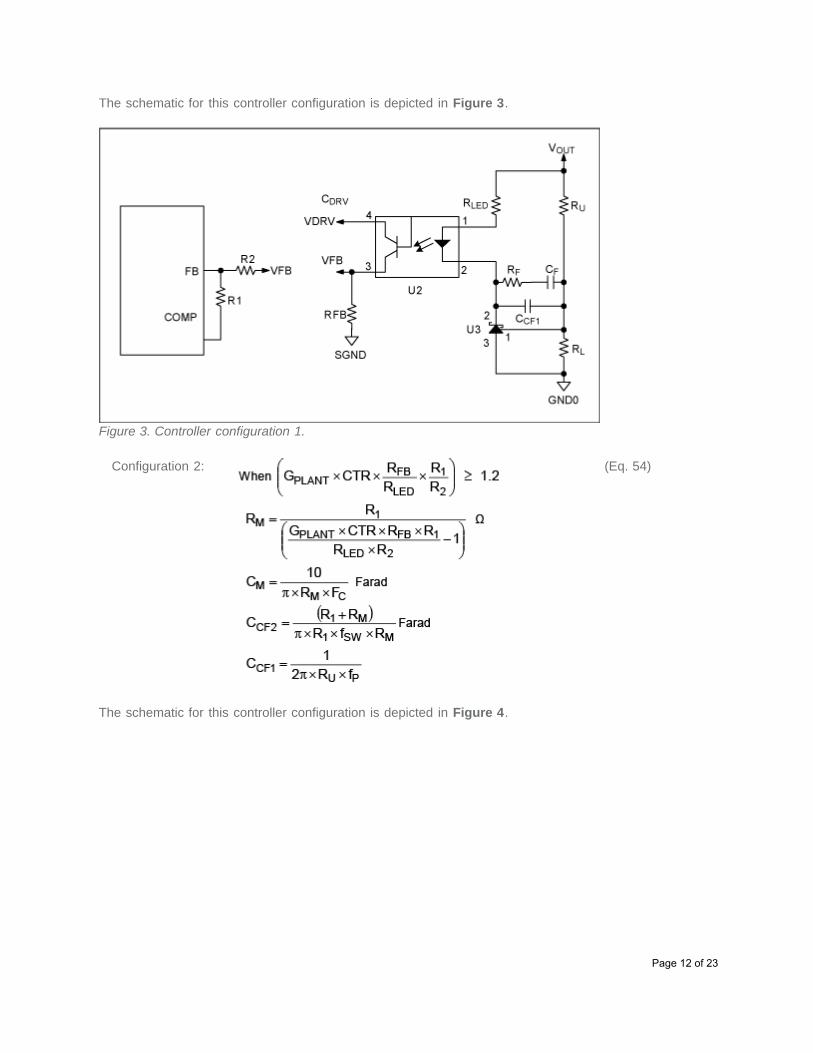
The schematic for this controller configuration is depicted in Figure 3.
Figure 3. Controller configuration 1.
Configuration 2: (Eq. 54)
The schematic for this controller configuration is depicted in Figure 4.
Page 12 of 23
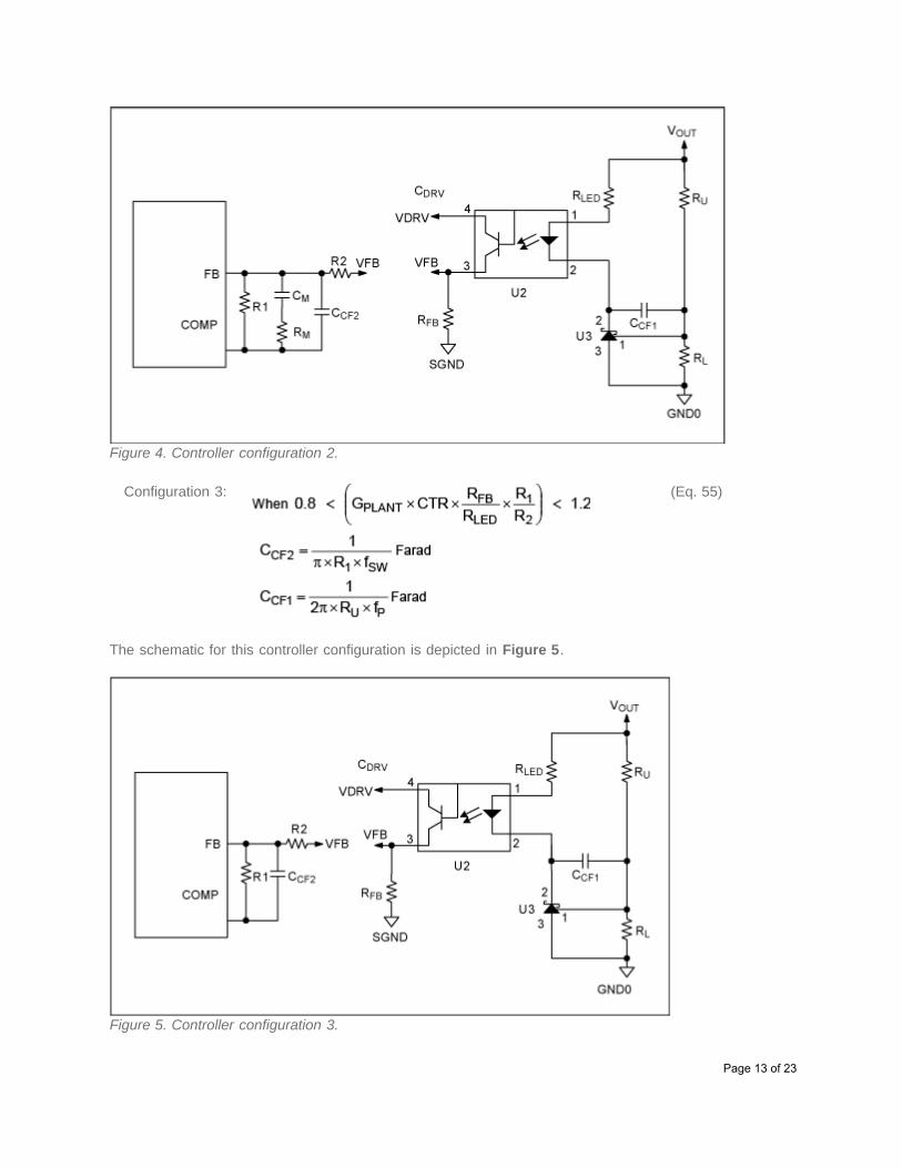
Figure 4. Controller configuration 2.
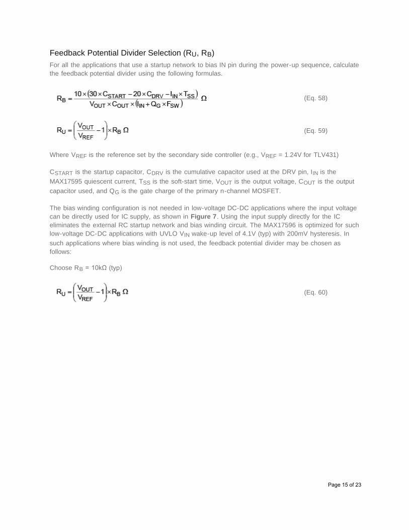
Configuration 3: (Eq. 55)
The schematic for this controller configuration is depicted in Figure 5.
Figure 5. Controller configuration 3.
Page 13 of 23

Bias Winding Supply ConfigurationThe MAX17595 is implemented with a 20V VIN UVLO wake-up level with 13V hysteresis to optimize thesize of bias capacitor. A simple RC circuit is used to start up the MAX17595. To sustain the operation ofthe circuit, the input supply to the IC is bootstrapped through diode D2 as shown in Figure 6 (refer tothe MAX17595–7 data sheet to design the startup network).
Figure 6. IN supply configuration for an offline isolated design.
Turns Ratio Calculation (NB/NP)The transformer turns ratio (KB = NB/NP) can be calculated as follows:
(Eq. 56)
Bias Capacitor (CSTART) CalculationIn isolated applications where a bias winding configuration is used to power up MAX17595/MAX17596,CSTART can be calculated as follows:
CSTART = 0.75 × (CDRV + 0.1 × IIN × TSS + 0.04 × TSS × QG × FSW) (Eq. 57)
Page 14 of 23
Feedback Potential Divider Selection (RU, RB)For all the applications that use a startup network to bias IN pin during the power-up sequence, calculatethe feedback potential divider using the following formulas.
(Eq. 58)
(Eq. 59)
Where VREF is the reference set by the secondary side controller (e.g., VREF = 1.24V for TLV431)
CSTART is the startup capacitor, CDRV is the cumulative capacitor used at the DRV pin, IIN is theMAX17595 quiescent current, TSS is the soft-start time, VOUT is the output voltage, COUT is the outputcapacitor used, and QG is the gate charge of the primary n-channel MOSFET.
The bias winding configuration is not needed in low-voltage DC-DC applications where the input voltagecan be directly used for IC supply, as shown in Figure 7. Using the input supply directly for the ICeliminates the external RC startup network and bias winding circuit. The MAX17596 is optimized for suchlow-voltage DC-DC applications with UVLO VIN wake-up level of 4.1V (typ) with 200mV hysteresis. Insuch applications where bias winding is not used, the feedback potential divider may be chosen asfollows:
Choose RB = 10kΩ (typ)
(Eq. 60)
Page 15 of 23
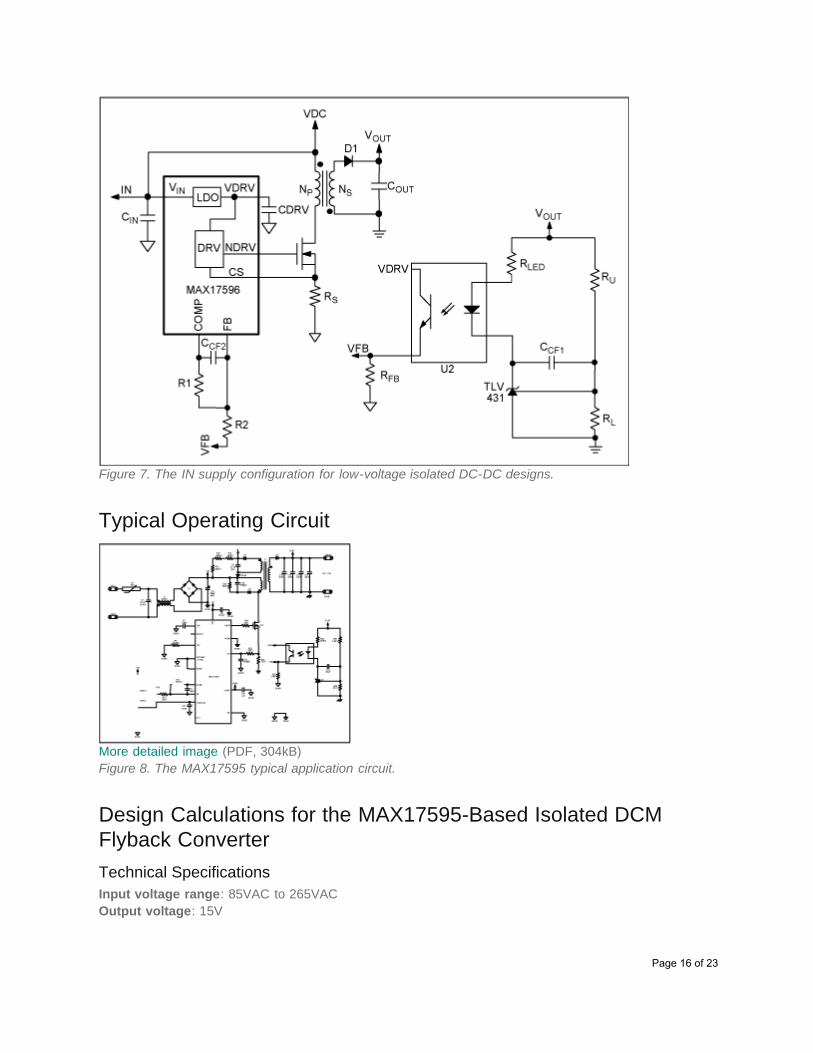
Figure 7. The IN supply configuration for low-voltage isolated DC-DC designs.
Typical Operating Circuit
More detailed image (PDF, 304kB)Figure 8. The MAX17595 typical application circuit.
Design Calculations for the MAX17595-Based Isolated DCMFlyback ConverterTechnical SpecificationsInput voltage range: 85VAC to 265VACOutput voltage: 15V
Page 16 of 23
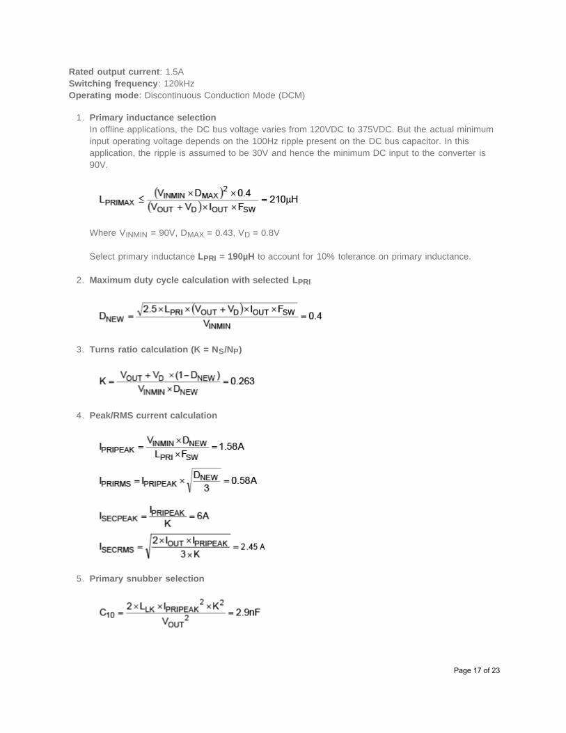
Rated output current: 1.5ASwitching frequency: 120kHzOperating mode: Discontinuous Conduction Mode (DCM)
1. Primary inductance selectionIn offline applications, the DC bus voltage varies from 120VDC to 375VDC. But the actual minimuminput operating voltage depends on the 100Hz ripple present on the DC bus capacitor. In thisapplication, the ripple is assumed to be 30V and hence the minimum DC input to the converter is90V.
Where VINMIN = 90V, DMAX = 0.43, VD = 0.8V
Select primary inductance LPRI = 190µH to account for 10% tolerance on primary inductance.
2. Maximum duty cycle calculation with selected LPRI
3. Turns ratio calculation (K = NS/NP)
4. Peak/RMS current calculation
5. Primary snubber selection
Page 17 of 23
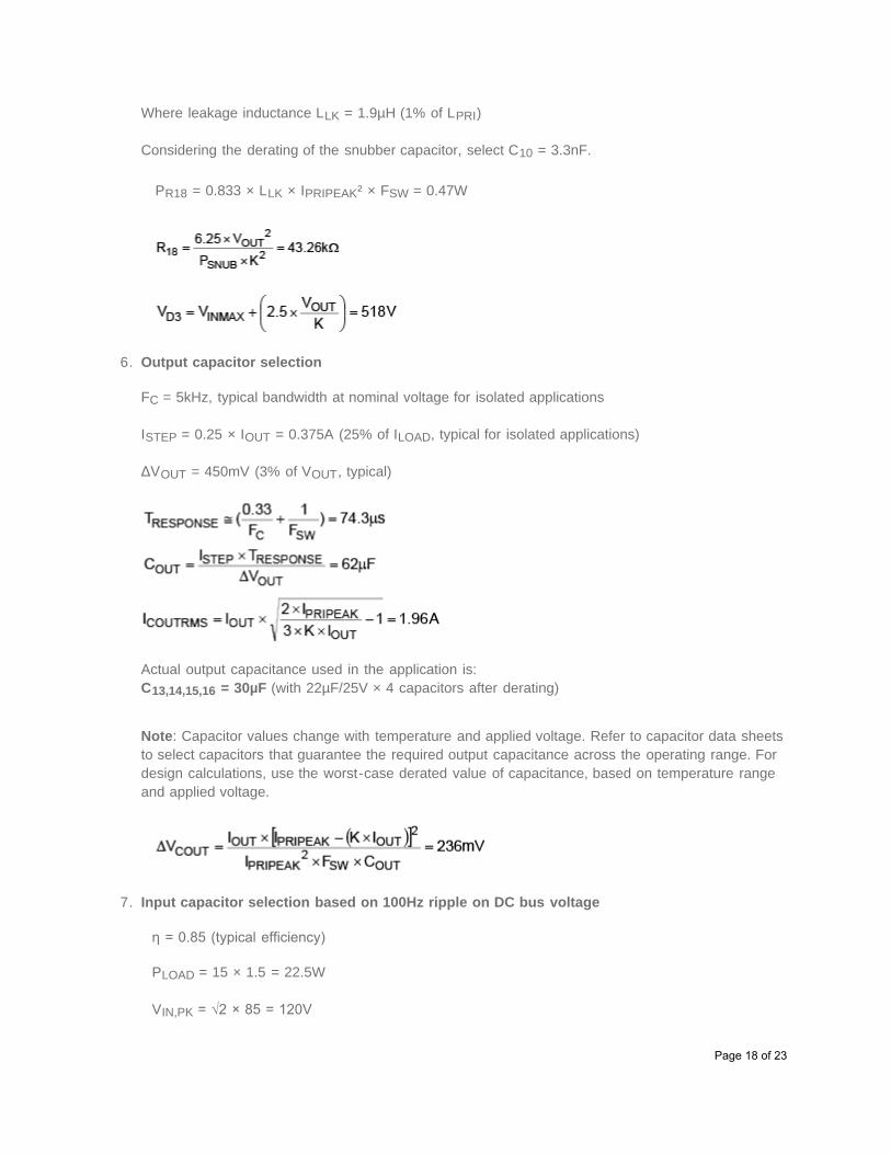
Where leakage inductance LLK = 1.9µH (1% of LPRI)
Considering the derating of the snubber capacitor, select C10 = 3.3nF.
PR18 = 0.833 × LLK × IPRIPEAK² × FSW = 0.47W
6. Output capacitor selection
FC = 5kHz, typical bandwidth at nominal voltage for isolated applications
ISTEP = 0.25 × IOUT = 0.375A (25% of ILOAD, typical for isolated applications)
ΔVOUT = 450mV (3% of VOUT, typical)
Actual output capacitance used in the application is:C13,14,15,16 = 30µF (with 22µF/25V × 4 capacitors after derating)
Note: Capacitor values change with temperature and applied voltage. Refer to capacitor data sheetsto select capacitors that guarantee the required output capacitance across the operating range. Fordesign calculations, use the worst-case derated value of capacitance, based on temperature rangeand applied voltage.
7. Input capacitor selection based on 100Hz ripple on DC bus voltage
η = 0.85 (typical efficiency)
PLOAD = 15 × 1.5 = 22.5W
VIN,PK = √2 × 85 = 120V
Page 18 of 23
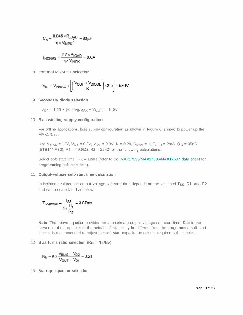
8. External MOSFET selection
9. Secondary diode selection
VD4 = 1.25 × (K × VINMAX + VOUT) = 140V
10. Bias winding supply configuration
For offline applications, bias supply configuration as shown in Figure 6 is used to power up theMAX17595.
Use VBIAS = 12V, VD2 = 0.8V, VD1 = 0.8V, K = 0.24, CDRV = 1µF, IIN = 2mA, QG = 35nC(STB11NM80), R1 = 49.9kΩ, R2 = 22kΩ for the following calculations.
Select soft-start time TSS = 12ms (refer to the MAX17595/MAX17596/MAX17597 data sheet forprogramming soft-start time).
11. Output-voltage soft-start time calculation
In isolated designs, the output-voltage soft-start time depends on the values of TSS, R1, and R2and can be calculated as follows:
Note: The above equation provides an approximate output-voltage soft-start time. Due to thepresence of the optocircuit, the actual soft-start may be different from the programmed soft-starttime. It is recommended to adjust the soft-start capacitor to get the required soft-start time.
12. Bias turns ratio selection (KB = NB/NP)
13. Startup capacitor selection
Page 19 of 23
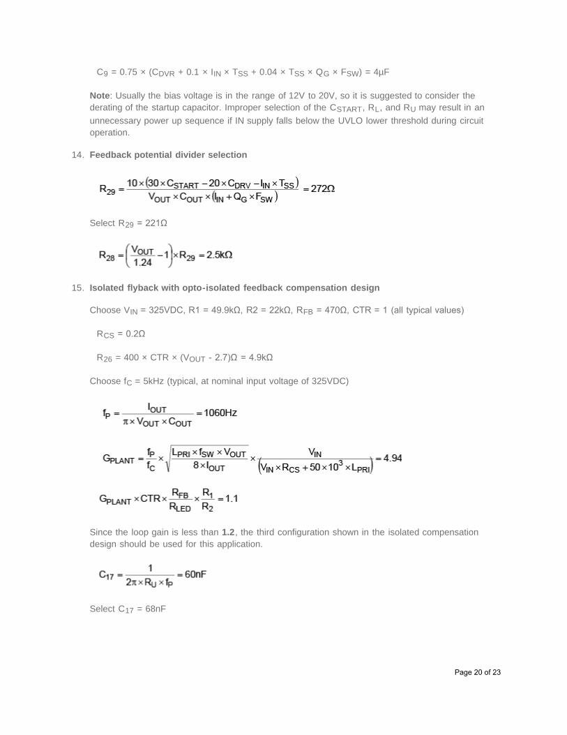
C9 = 0.75 × (CDVR + 0.1 × IIN × TSS + 0.04 × TSS × QG × FSW) = 4µF
Note: Usually the bias voltage is in the range of 12V to 20V, so it is suggested to consider thederating of the startup capacitor. Improper selection of the CSTART, RL, and RU may result in anunnecessary power up sequence if IN supply falls below the UVLO lower threshold during circuitoperation.
14. Feedback potential divider selection
Select R29 = 221Ω
15. Isolated flyback with opto-isolated feedback compensation design
Choose VIN = 325VDC, R1 = 49.9kΩ, R2 = 22kΩ, RFB = 470Ω, CTR = 1 (all typical values)
RCS = 0.2Ω
R26 = 400 × CTR × (VOUT - 2.7)Ω = 4.9kΩ
Choose fC = 5kHz (typical, at nominal input voltage of 325VDC)
Since the loop gain is less than 1.2, the third configuration shown in the isolated compensationdesign should be used for this application.
Select C17 = 68nF
Page 20 of 23
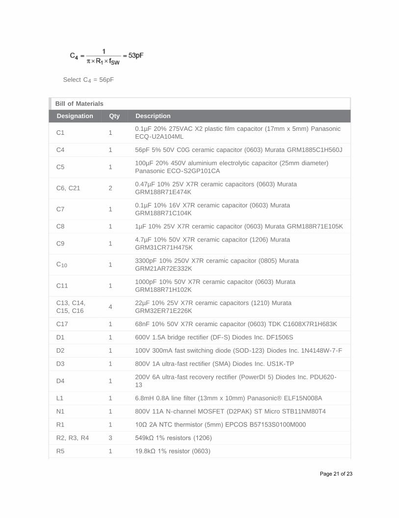
Select C4 = 56pF
Bill of Materials
Designation Qty Description
C1 1 0.1µF 20% 275VAC X2 plastic film capacitor (17mm x 5mm) PanasonicECQ-U2A104ML
C4 1 56pF 5% 50V C0G ceramic capacitor (0603) Murata GRM1885C1H560J
C5 1 100µF 20% 450V aluminium electrolytic capacitor (25mm diameter)Panasonic ECO-S2GP101CA
C6, C21 2 0.47µF 10% 25V X7R ceramic capacitors (0603) MurataGRM188R71E474K
C7 1 0.1µF 10% 16V X7R ceramic capacitor (0603) MurataGRM188R71C104K
C8 1 1µF 10% 25V X7R ceramic capacitor (0603) Murata GRM188R71E105K
C9 1 4.7µF 10% 50V X7R ceramic capacitor (1206) MurataGRM31CR71H475K
C10 1 3300pF 10% 250V X7R ceramic capacitor (0805) MurataGRM21AR72E332K
C11 1 1000pF 10% 50V X7R ceramic capacitor (0603) MurataGRM188R71H102K
C13, C14,C15, C16 4 22µF 10% 25V X7R ceramic capacitors (1210) Murata
GRM32ER71E226K
C17 1 68nF 10% 50V X7R ceramic capacitor (0603) TDK C1608X7R1H683K
D1 1 600V 1.5A bridge rectifier (DF-S) Diodes Inc. DF1506S
D2 1 100V 300mA fast switching diode (SOD-123) Diodes Inc. 1N4148W-7-F
D3 1 800V 1A ultra-fast rectifier (SMA) Diodes Inc. US1K-TP
D4 1 200V 6A ultra-fast recovery rectifier (PowerDI 5) Diodes Inc. PDU620-13
L1 1 6.8mH 0.8A line filter (13mm x 10mm) Panasonic® ELF15N008A
N1 1 800V 11A N-channel MOSFET (D2PAK) ST Micro STB11NM80T4
R1 1 10Ω 2A NTC thermistor (5mm) EPCOS B57153S0100M000
R2, R3, R4 3 549kΩ 1% resistors (1206)
R5 1 19.8kΩ 1% resistor (0603)
Page 21 of 23
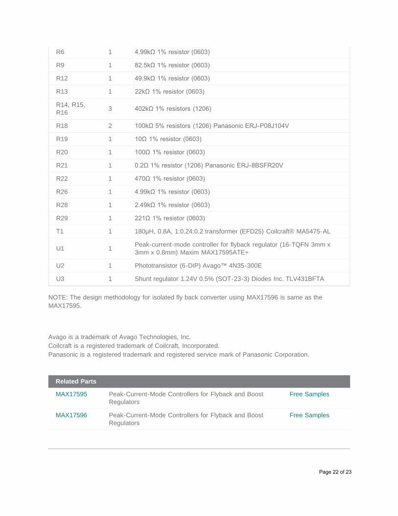
R6 1 4.99kΩ 1% resistor (0603)
R9 1 82.5kΩ 1% resistor (0603)
R12 1 49.9kΩ 1% resistor (0603)
R13 1 22kΩ 1% resistor (0603)
R14, R15,R16 3 402kΩ 1% resistors (1206)
R18 2 100kΩ 5% resistors (1206) Panasonic ERJ-P08J104V
R19 1 10Ω 1% resistor (0603)
R20 1 100Ω 1% resistor (0603)
R21 1 0.2Ω 1% resistor (1206) Panasonic ERJ-8BSFR20V
R22 1 470Ω 1% resistor (0603)
R26 1 4.99kΩ 1% resistor (0603)
R28 1 2.49kΩ 1% resistor (0603)
R29 1 221Ω 1% resistor (0603)
T1 1 180µH, 0.8A, 1:0.24:0.2 transformer (EFD25) Coilcraft® MA5475-AL
U1 1 Peak-current-mode controller for flyback regulator (16-TQFN 3mm x3mm x 0.8mm) Maxim MAX17595ATE+
U2 1 Phototransistor (6-DIP) Avago™ 4N35-300E
U3 1 Shunt regulator 1.24V 0.5% (SOT-23-3) Diodes Inc. TLV431BFTA
NOTE: The design methodology for isolated fly back converter using MAX17596 is same as theMAX17595.
Avago is a trademark of Avago Technologies, Inc.Coilcraft is a registered trademark of Coilcraft, Incorporated.Panasonic is a registered trademark and registered service mark of Panasonic Corporation.
Related Parts
MAX17595 Peak-Current-Mode Controllers for Flyback and BoostRegulators
Free Samples
MAX17596 Peak-Current-Mode Controllers for Flyback and BoostRegulators
Free Samples
Page 22 of 23

More InformationFor Technical Support: http://www.maximintegrated.com/supportFor Samples: http://www.maximintegrated.com/samplesOther Questions and Comments: http://www.maximintegrated.com/contact
Application Note 5504: http://www.maximintegrated.com/an5504APPLICATION NOTE 5504, AN5504, AN 5504, APP5504, Appnote5504, Appnote 5504 © 2013 Maxim Integrated Products, Inc.Additional Legal Notices: http://www.maximintegrated.com/legal
Page 23 of 23


![Catalogue FLYBACK Equivalent - [PDF Document] FLYBACK Equivalent FlyBack Equivalent flyback reemplazo conversor Flyback tv fly-back Flyback Tester Flyback Converter conversor Flyback](https://img.pdfslide.net/doc/110x75/5a832a447f8b9a9d308e9416/catalogue-flyback-equivalent-pdf-document-flyback-equivalent-flyback-equivalent.jpg)