Embed Size (px)
Citation preview
Exercise Manual for
Quartus® II Software Design Series: Timing Analysis
Software requirements to complete all exercises
Software Requirements: Quartus II software version 9.1
Link to the Quartus II Handbook: http://www.altera.com/literature/hb/qts/quartusii_handbook.pdf
Use the link below to download the design files for the exercises: http://www.altera.com/customertraining/ILT/Quartus II Design Series_Timing_9_1_v2.zip

Exercises Quartus II Software Design Series: Timing Analysis
Copyright © 2010 Altera Corporation A-MNL-QII-TA-EX-9-1-v2
2
Quartus II Software Design Series: Timing Analysis Exercises
Copyright © 2010 Altera Corporation A-MNL-QII-TA-EX-9-1-v2
3
Exercise 1
Introduction to the TimeQuest Tool

Exercises Quartus II Software Design Series: Timing Analysis
Copyright © 2010 Altera Corporation A-MNL-QII-TA-EX-9-1-v2
4
Quartus II Software Design Series: Timing Analysis Exercises
Copyright © 2010 Altera Corporation A-MNL-QII-TA-EX-9-1-v2
5
Exercise 1
Objective:
• Given an existing SDC file, follow the TimeQuest flow to generate timing reports
• Learn about using the TimeQuest interface
As you proceed through the exercises, be sure to completely read the instructions for each step and sub-step in this lab manual. Each step first summarizes what you’ll be doing in that step before providing complete instructions. Use the lines next to each step (____) to keep track of your progress or to check off completed steps in the exercises.
If you have any questions or problems, please ask the instructor for assistance.
Exercises Quartus II Software Design Series: Timing Analysis
Copyright © 2010 Altera Corporation A-MNL-QII-TA-EX-9-1-v2
6
Step 1: Open and synthesize a project
To get started with using TimeQuest timing analysis, you will open a simple project and configure it to use an existing SDC file with the TimeQuest timing analyzer.
____ 1. Unzip the lab project files, if necessary. In an Explorer window, go to C:\altera_trn\Quartus_II_Software_Design_Series_Timing_Analysis. The name of the directory may be shortened to Quartus II Timing or similar on some machines. This will be your lab installation directory. Delete any old lab file folders that may already exist there labeled QIIT9_1. Double-click the executable file (Quartus II Design Series_Timing_Analysis_9_1_v1.exe) found in that location. If you still cannot find this file, ask your instructor for assistance. In the WinZip dialog box, just click Unzip to automatically extract the files in place to a new folder named QIIT9_1 in the directory mentioned above.
____ 2. Start the Quartus II software version 9.1 from the Altera program folder in the Windows Start menu.
____ 3. Open the project pipemult.qpf located in the <lab_install_directory>\QIIT9_1\Intro directory. Remember to use the Open Project command from the File menu instead of the Open command (which is used for opening individual files instead of entire projects).
____ 4. Click to synthesize the design.
Though you could also perform a full compilation since this design is complete, you’re going to follow the TimeQuest flow as if you were working on a new design that requires a long place and route. Performing just synthesis allows you to quickly generate a netlist in order to start constraining the design.
Quartus II Software Design Series: Timing Analysis Exercises
Copyright © 2010 Altera Corporation A-MNL-QII-TA-EX-9-1-v2
7
Step 2: Start the TimeQuest GUI and create timing netlist for analysis
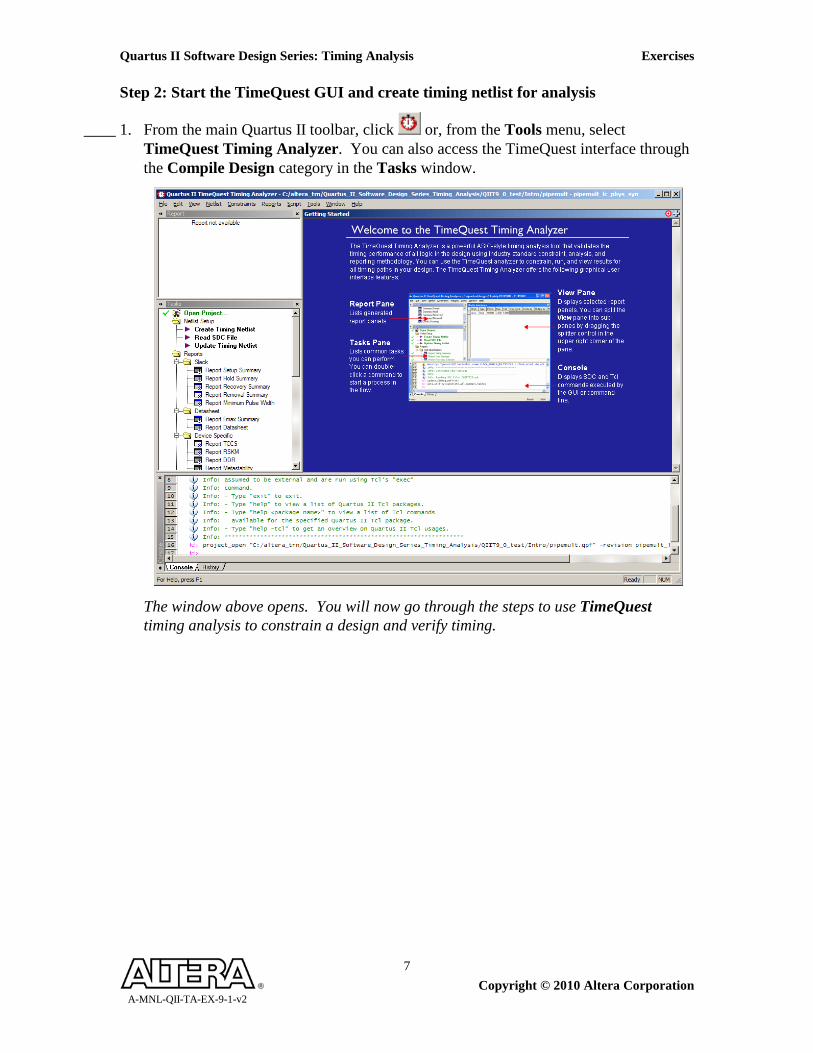
____ 1. From the main Quartus II toolbar, click or, from the Tools menu, select TimeQuest Timing Analyzer. You can also access the TimeQuest interface through the Compile Design category in the Tasks window.
The window above opens. You will now go through the steps to use TimeQuest timing analysis to constrain a design and verify timing.
Exercises Quartus II Software Design Series: Timing Analysis
Copyright © 2010 Altera Corporation A-MNL-QII-TA-EX-9-1-v2
8
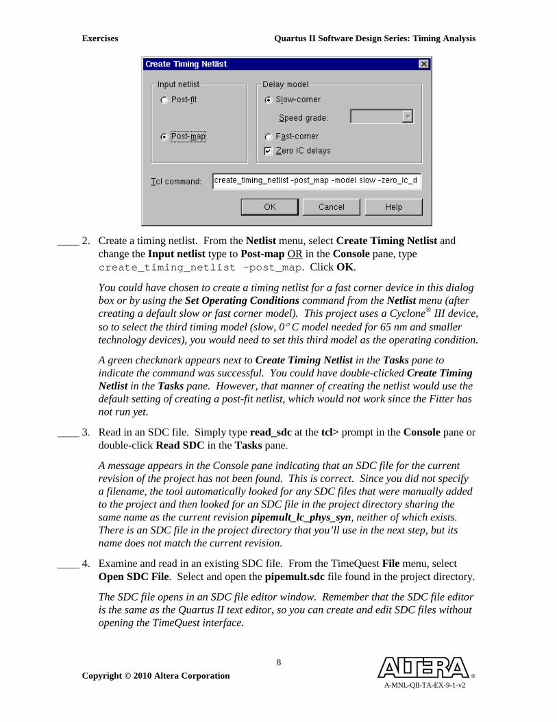
____ 2. Create a timing netlist. From the Netlist menu, select Create Timing Netlist and
change the Input netlist type to Post-map OR in the Console pane, type create_timing_netlist –post_map. Click OK.
You could have chosen to create a timing netlist for a fast corner device in this dialog box or by using the Set Operating Conditions command from the Netlist menu (after creating a default slow or fast corner model). This project uses a Cyclone® III device, so to select the third timing model (slow, 0° C model needed for 65 nm and smaller technology devices), you would need to set this third model as the operating condition.
A green checkmark appears next to Create Timing Netlist in the Tasks pane to indicate the command was successful. You could have double-clicked Create Timing Netlist in the Tasks pane. However, that manner of creating the netlist would use the default setting of creating a post-fit netlist, which would not work since the Fitter has not run yet.
____ 3. Read in an SDC file. Simply type read_sdc at the tcl> prompt in the Console pane or double-click Read SDC in the Tasks pane.
A message appears in the Console pane indicating that an SDC file for the current revision of the project has not been found. This is correct. Since you did not specify a filename, the tool automatically looked for any SDC files that were manually added to the project and then looked for an SDC file in the project directory sharing the same name as the current revision pipemult_lc_phys_syn, neither of which exists. There is an SDC file in the project directory that you’ll use in the next step, but its name does not match the current revision.
____ 4. Examine and read in an existing SDC file. From the TimeQuest File menu, select Open SDC File. Select and open the pipemult.sdc file found in the project directory.
The SDC file opens in an SDC file editor window. Remember that the SDC file editor is the same as the Quartus II text editor, so you can create and edit SDC files without opening the TimeQuest interface.
Quartus II Software Design Series: Timing Analysis Exercises
Copyright © 2010 Altera Corporation A-MNL-QII-TA-EX-9-1-v2
9
Examine the constraints found in the pipemult.sdc file. These constraints constrain the input clock and the I/O signals in the design. These constraints fully constrain this simple design. We’ll talk much more about constraints and creating them later.
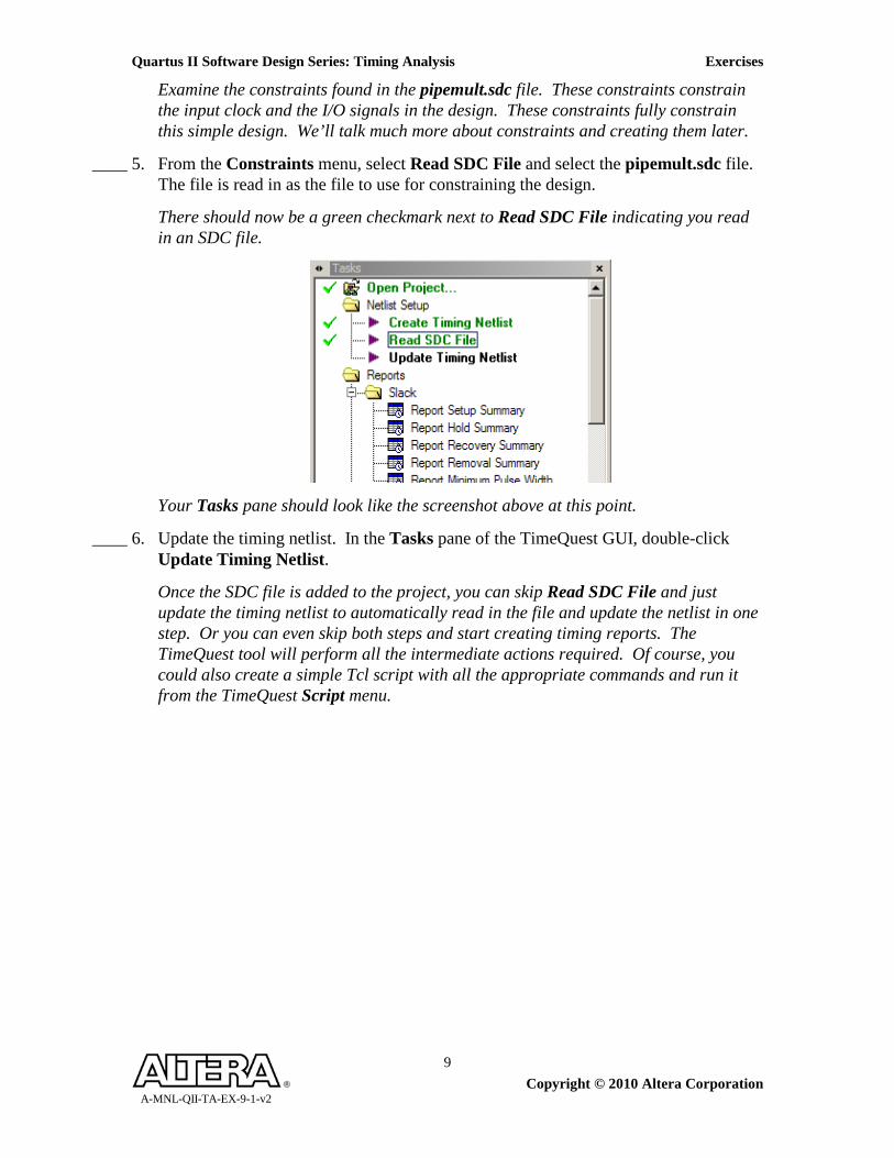
____ 5. From the Constraints menu, select Read SDC File and select the pipemult.sdc file. The file is read in as the file to use for constraining the design.
There should now be a green checkmark next to Read SDC File indicating you read in an SDC file.
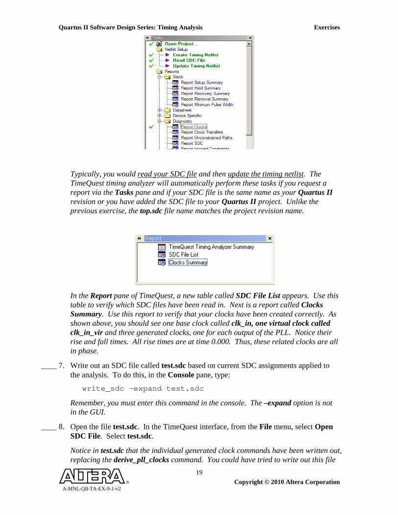
Your Tasks pane should look like the screenshot above at this point.
____ 6. Update the timing netlist. In the Tasks pane of the TimeQuest GUI, double-click Update Timing Netlist.
Once the SDC file is added to the project, you can skip Read SDC File and just update the timing netlist to automatically read in the file and update the netlist in one step. Or you can even skip both steps and start creating timing reports. The TimeQuest tool will perform all the intermediate actions required. Of course, you could also create a simple Tcl script with all the appropriate commands and run it from the TimeQuest Script menu.
Exercises Quartus II Software Design Series: Timing Analysis
Copyright © 2010 Altera Corporation A-MNL-QII-TA-EX-9-1-v2
10
Step 3: Use TimeQuest reports to verify design meeting timing
Now that the netlist has been updated, you can begin generating various reports. We’ll look at reports in more detail later. For now, experiment and explore the different reports you can create.
____ 1. In the Tasks pane, double-click Report SDC.
In the Report pane, a new folder called SDC Assignments appears containing three reports called Create Clock, Set Input Delay, and Set Output Delay. This report lists all the SDC constraints entered by the SDC file.
____ 2. In the Tasks pane, double-click Report Clocks.
This report verifies that clocks in the design are constrained correctly.
____ 3. In the Tasks pane, double-click Report Setup Summary.
This design meets setup timing.
____ 4. In the Tasks pane, double-click Report Hold Summary.
Uh oh. It looks like the design, even with the timing constraints added, just fails hold timing, indicated by the clock domain in red and a negative slack value. This is close enough that it can be fixed by using physical synthesis in the project to optimize the design’s placement and routing. We’ll see it fixed later when we create the same report using the post-fit netlist. For now, ignore the failure.
Step 4: Use the SDC file to guide the Quartus II fitter
____ 1. Bring the Quartus II software to the foreground.
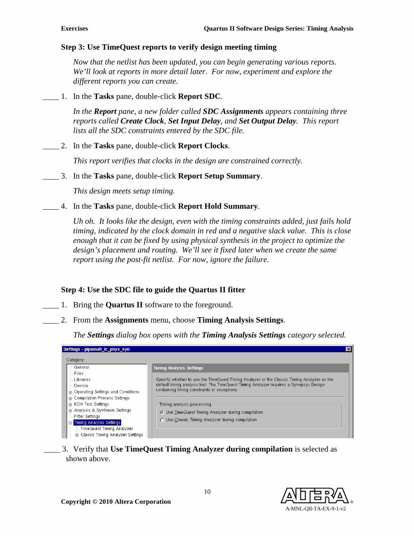
____ 2. From the Assignments menu, choose Timing Analysis Settings.
The Settings dialog box opens with the Timing Analysis Settings category selected.
____ 3. Verify that Use TimeQuest Timing Analyzer during compilation is selected as
shown above.
Quartus II Software Design Series: Timing Analysis Exercises
Copyright © 2010 Altera Corporation A-MNL-QII-TA-EX-9-1-v2
11
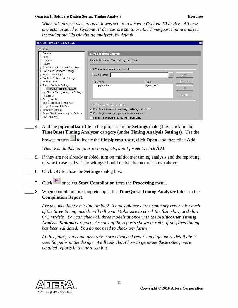
When this project was created, it was set up to target a Cyclone III device. All new projects targeted to Cyclone III devices are set to use the TimeQuest timing analyzer, instead of the Classic timing analyzer, by default.
____ 4. Add the pipemult.sdc file to the project. In the Settings dialog box, click on the
TimeQuest Timing Analyzer category (under Timing Analysis Settings). Use the
browse button to locate the file pipemult.sdc, click Open, and then click Add.
When you do this for your own projects, don’t forget to click Add!
____ 5. If they are not already enabled, turn on multicorner timing analysis and the reporting of worst-case paths. The settings should match the picture shown above.
____ 6. Click OK to close the Settings dialog box.
____ 7. Click or select Start Compilation from the Processing menu.
____ 8. When compilation is complete, open the TimeQuest Timing Analyzer folder in the Compilation Report.
Are you meeting or missing timing? A quick glance of the summary reports for each of the three timing models will tell you. Make sure to check the fast, slow, and slow 0°C models. You can check all three models at once with the Multicorner Timing Analysis Summary report. Are any of the reports shown in red? If not, then timing has been validated. You do not need to check any further.
At this point, you could generate more advanced reports and get more detail about specific paths in the design. We’ll talk about how to generate these other, more detailed reports in the next section.

Exercises Quartus II Software Design Series: Timing Analysis
Copyright © 2010 Altera Corporation A-MNL-QII-TA-EX-9-1-v2
12
Exercise Summary
• Practiced basic steps for using the TimeQuest timing analyzer with the Quartus II software
END OF EXERCISE 1
Quartus II Software Design Series: Timing Analysis Exercises
Copyright © 2010 Altera Corporation A-MNL-QII-TA-EX-9-1-v2
13
Exercise 2
Timing Analysis: Clock Constraints

Exercises Quartus II Software Design Series: Timing Analysis
Copyright © 2010 Altera Corporation A-MNL-QII-TA-EX-9-1-v2
14
Quartus II Software Design Series: Timing Analysis Exercises
Copyright © 2010 Altera Corporation A-MNL-QII-TA-EX-9-1-v2
15
Exercise 2
Objectives:
• Create a new SDC file
• Use SDC to constrain the clocks in a design containing PLLs
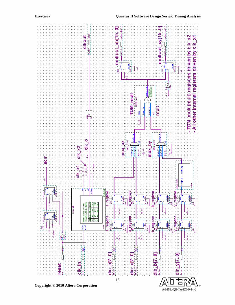
Top-Level Design: The design used for the rest of the exercises in this training (shown on the following page) multiplies two sets of 8-bit data inputs: din_a * din_b and din_x * din_y*. Along with this data input, the design also receives a board clock named clk_in running at 142.86 MHz (clock period of 7 ns) and an asynchronous reset named reset. To save on multiplier space, the data is time-domain multiplexed through a single multiplier running at twice the clock speed (285.71 MHz). All clocks for the design are generated by a PLL called main_pll with 3 output clocks. A 142.86 MHz PLL output called clk_x1 is used to reduce clock tree delay to internal registers. A 285.71 MHz PLL output called clk_x2 drives the multiplier at twice the input frequency. A second 142.86 MHz output from the PLL called c100_out drives the output port, clk_out. The resulting data output named multout_ab and multout_xy is center-aligned with clk_out (by means of the PLL) and then sent off-chip to another device on the board.
NOTE: Throughout the remaining exercises, you will be asked to create SDC commands without being directly guided by the instructions. It is up to you to figure out the correct commands using the training presentation material as well as the GUI tools and help information available in the TimeQuest timing analyzer. However, all SDC answers can be found in the file top.sdc, located in the Solutions\Timing subdirectory of the exercise installation directory. The solutions there are only examples, and the file itself cannot be used as the final .sdc file for the exercises. The format of your SDC commands may be different yet equivalent to the commands found in that file. If you are stuck or do not understand a solution command, please ask your instructor for assistance. The answer values for other questions in the exercises can be found in the file: Quartus II Design Series_Timing_9_1_Exercise_Solutions.doc located in the same subdirectory.
Exercises Quartus II Software Design Series: Timing Analysis
Copyright © 2010 Altera Corporation A-MNL-QII-TA-EX-9-1-v2
16
Quartus II Software Design Series: Timing Analysis Exercises
Copyright © 2010 Altera Corporation A-MNL-QII-TA-EX-9-1-v2
17
Step 1: Create SDC file for the design
In this step, you will open the project and locate and constrain all the design clocks.
____ 1. If it’s not already open, start the Quartus II software version 9.1 from the Altera program folder in the Windows Start menu. Open the project top.qpf located in the <lab_install_directory>\QIIV9_1\Timing directory.
____ 2. Open the file top.bdf by double-clicking top in the Project Navigator or through the Open command in the File menu.
You should see the schematic from the previous page of this exercise manual.
____ 3. Synthesize the design. Click the button or, from the Processing menu, choose Start ⇒ Start Analysis & Synthesis. Click OK when finished.
Remember, we’re only at the point of adding constraints, so there is no need to perform a full compilation. So you can synthesize, generate a timing netlist, and begin constraining the design with the node names from that database.
____ 4. Open the TimeQuest timing analyzer. Click the button or from the Tools menu, select TimeQuest Timing Analyzer.
____ 5. Create a slow model timing netlist. In the TimeQuest tool, from the Netlist menu, select Create Timing Netlist. Change the Input netlist type to Post-map OR in the Console pane, type create_timing_netlist –post_map –model slow.
Remember, you must use the -post_map netlist type because you only performed synthesis (no fitting) and you cannot access the -post_map option from the Create Timing Netlist task in the Tasks pane.
____ 6. If one hasn’t already been created, create a new file called top.sdc. Select File ⇒ New SDC File. Select File ⇒ Save As and save the file as <lab_install_directory>\QIIV9_1\Timing\top.sdc.
Notice that an option, Add file to current project, is turned on in the Save As dialog box.
Exercises Quartus II Software Design Series: Timing Analysis
Copyright © 2010 Altera Corporation A-MNL-QII-TA-EX-9-1-v2
18
Step 2: Create base and generated clock constraints
Next, as with many other steps in this exercise, you will be adding a constraint to your top.sdc file. You will only be told what to constrain and given values. It will be up to you to use the proper SDC command.
Feel free to type the SDC command directly into the SDC File Editor or use the Insert Constraint submenu of the SDC File Editor’s Edit menu, whichever you feel more comfortable with. It is recommended that you enter all constraints in the SDC File Editor instead of trying to enter constraints directly into the Console pane. This makes it much easier to create, edit, and manage your constraints.
____ 1. In the top.sdc file, assign a 7-ns clock to the input port clk_in. Use the default name clk_in as the name of the clock.
Access the constraint GUI dialog boxes from the the Insert Constraint submenu of the Edit menu. The GUI will place the constraint at the current location of the cursor, so remember to create new lines before accessing the dialog boxes. The GUI constraint dialog boxes can be used for almost all the constraints you’ll be creating. However, remember from the presentation that there are some constraint options and arguments that are not in the GUI. You can always refer back to the presentation slides to find a constraint option that you may need.
____ 2. (Optional) On the line above the create_clock command you’ve just created, insert a comment using # to indicate what the succeeding SDC command is doing. This is just good coding practice, and it may be helpful if you need to go back and review the constraints you’ve entered.
____ 3. In the top.sdc file, create a 7-ns virtual clock, named clk_in_vir.
____ 4. In top.sdc, add the command to automatically create generated clocks on all of the PLL outputs based on your previously specified clock input. Hint: this is an SDC extension command that does not require any optional arguments (and is not accessible through the GUI).
A hint for an even shorter shortcut: Instead of using the create_clock command (as instructed in #1 above) to create your base clock, you could use an optional argument with the command used in this step.
____ 5. Save and close top.sdc.
____ 6. Double-click Report Clocks (Tasks pane ⇒ Reports ⇒ Diagnostic Reports).
Quartus II Software Design Series: Timing Analysis Exercises
Copyright © 2010 Altera Corporation A-MNL-QII-TA-EX-9-1-v2
19
Typically, you would read your SDC file and then update the timing netlist. The TimeQuest timing analyzer will automatically perform these tasks if you request a report via the Tasks pane and if your SDC file is the same name as your Quartus II revision or you have added the SDC file to your Quartus II project. Unlike the previous exercise, the top.sdc file name matches the project revision name.
In the Report pane of TimeQuest, a new table called SDC File List appears. Use this table to verify which SDC files have been read in. Next is a report called Clocks Summary. Use this report to verify that your clocks have been created correctly. As shown above, you should see one base clock called clk_in, one virtual clock called clk_in_vir and three generated clocks, one for each output of the PLL. Notice their rise and fall times. All rise times are at time 0.000. Thus, these related clocks are all in phase.
____ 7. Write out an SDC file called test.sdc based on current SDC assignments applied to the analysis. To do this, in the Console pane, type:
write_sdc -expand test.sdc
Remember, you must enter this command in the console. The –expand option is not in the GUI.
____ 8. Open the file test.sdc. In the TimeQuest interface, from the File menu, select Open SDC File. Select test.sdc.
Notice in test.sdc that the individual generated clock commands have been written out, replacing the derive_pll_clocks command. You could have tried to write out this file
Exercises Quartus II Software Design Series: Timing Analysis
Copyright © 2010 Altera Corporation A-MNL-QII-TA-EX-9-1-v2
20
from the Tasks pane or the Constraints menu. However, the derive_pll_clocks constraint would not have been expanded since the -expand option would not be used.
____ 9. Open the file top.sdc.
____ 10. Copy the 3 create_generated_clock commands from test.sdc into top.sdc. In top.sdc, make sure you comment out the derive_pll_clocks command.
Note that this is not necessary. You could simply keep the derive_pll_clocks command in your SDC file. The advantage of keeping the command is that whenever the PLL settings are changed, the generated clock commands are updated automatically. However, you can’t rename the generated clocks to something more meaningful, which is what you will do next. Also, derive_pll_clocks is not a standard SDC command and will typically not be recognized by other tools that support SDC.
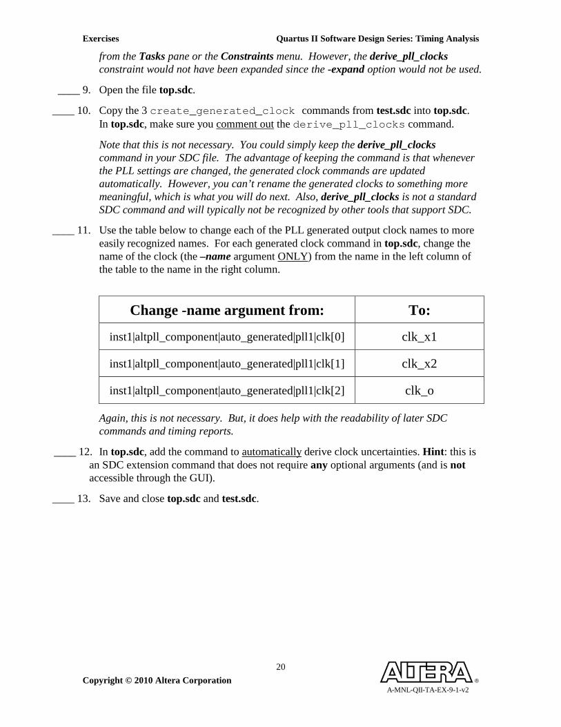
____ 11. Use the table below to change each of the PLL generated output clock names to more easily recognized names. For each generated clock command in top.sdc, change the name of the clock (the –name argument ONLY) from the name in the left column of the table to the name in the right column.
Change -name argument from: To:
inst1|altpll_component|auto_generated|pll1|clk[0] clk_x1
inst1|altpll_component|auto_generated|pll1|clk[1] clk_x2
inst1|altpll_component|auto_generated|pll1|clk[2] clk_o
Again, this is not necessary. But, it does help with the readability of later SDC commands and timing reports.
____ 12. In top.sdc, add the command to automatically derive clock uncertainties. Hint: this is an SDC extension command that does not require any optional arguments (and is not accessible through the GUI).
____ 13. Save and close top.sdc and test.sdc.
Quartus II Software Design Series: Timing Analysis Exercises
Copyright © 2010 Altera Corporation A-MNL-QII-TA-EX-9-1-v2
21
____ 14. Reset the design. To do this, do ONE of the following:
a. From the Constraints menu, select Reset Design.
b. Double-click Reset Design at the bottom of the Tasks pane.
c. In the Console pane, type reset_design.
Resetting the design tells the timing analyzer to flush all timing constraints from the netlist, thus allowing you to “start over” with new constraints on the same netlist. It is analogous to deleting the timing netlist and creating a new netlist of the same type.
You should now see that all of your reports have been deleted.
____ 15. Run Report Clocks again.
Your clocks should match all the clock names you entered in the SDC file.
____ 16. Run Report SDC and click on the Set Clock Uncertainty Table to observe the clock uncertainties derived for you.
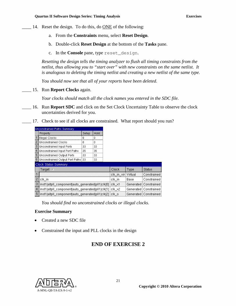
____ 17. Check to see if all clocks are constrained. What report should you run?
You should find no unconstrained clocks or illegal clocks.
Exercise Summary
• Created a new SDC file • Constrained the input and PLL clocks in the design
END OF EXERCISE 2

Exercises Quartus II Software Design Series: Timing Analysis
Copyright © 2010 Altera Corporation A-MNL-QII-TA-EX-9-1-v2
22
Quartus II Software Design Series: Timing Analysis Exercises
Copyright © 2010 Altera Corporation A-MNL-QII-TA-EX-9-1-v2
23
Exercise 3
Timing Analysis: Synchronous Input
Constraints

Exercises Quartus II Software Design Series: Timing Analysis
Copyright © 2010 Altera Corporation A-MNL-QII-TA-EX-9-1-v2
24
Exercise 3
Objective:
• Constrain the synchronous input paths in the design
Quartus II Software Design Series: Timing Analysis Exercises
Copyright © 2010 Altera Corporation A-MNL-QII-TA-EX-9-1-v2
25
Step 1: Constrain Synchronous Input paths using SDC
Now we need to define the FPGA’s input timing relative to external devices.
____ 1. Open top.sdc.
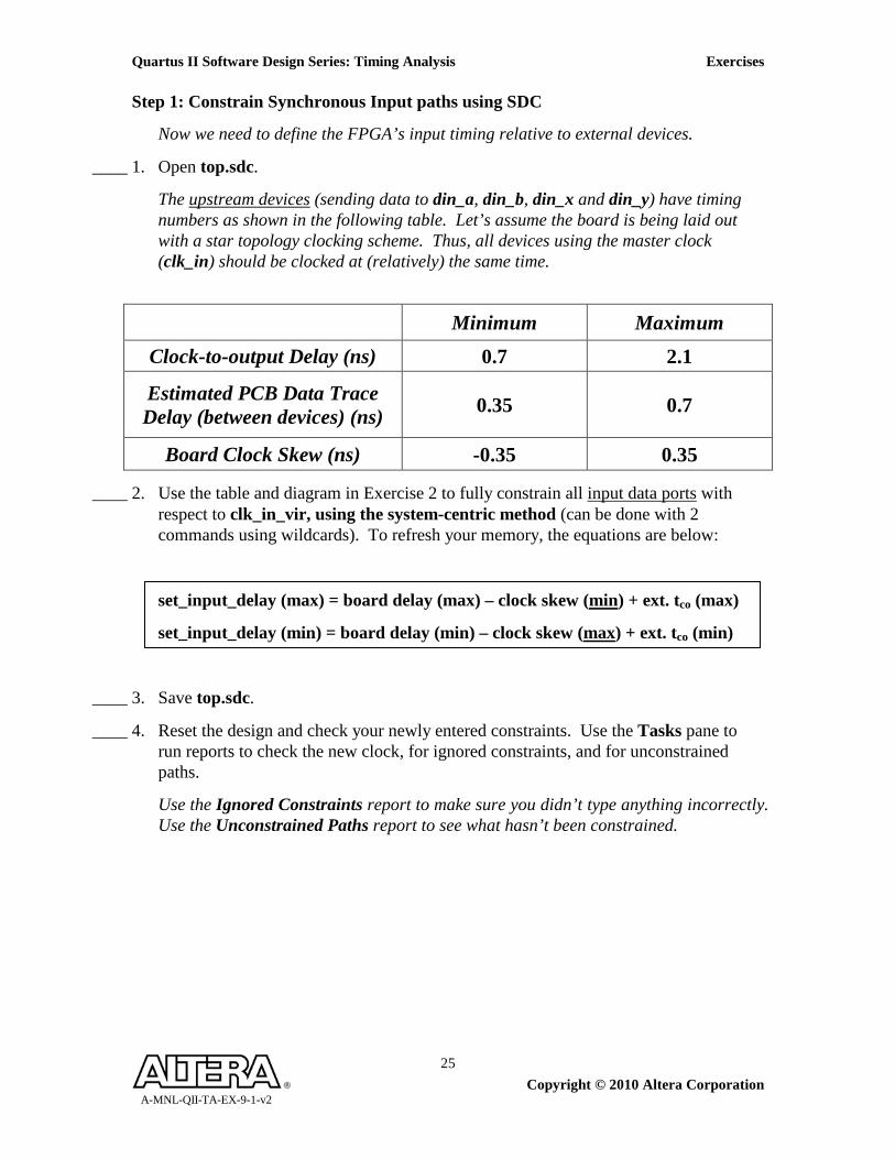
The upstream devices (sending data to din_a, din_b, din_x and din_y) have timing numbers as shown in the following table. Let’s assume the board is being laid out with a star topology clocking scheme. Thus, all devices using the master clock (clk_in) should be clocked at (relatively) the same time.
Minimum Maximum Clock-to-output Delay (ns) 0.7 2.1
Estimated PCB Data Trace Delay (between devices) (ns) 0.35 0.7
Board Clock Skew (ns) -0.35 0.35
____ 2. Use the table and diagram in Exercise 2 to fully constrain all input data ports with respect to clk_in_vir, using the system-centric method (can be done with 2 commands using wildcards). To refresh your memory, the equations are below:
set_input_delay (max) = board delay (max) – clock skew (min) + ext. tco (max)
set_input_delay (min) = board delay (min) – clock skew (max) + ext. tco (min)
____ 3. Save top.sdc.
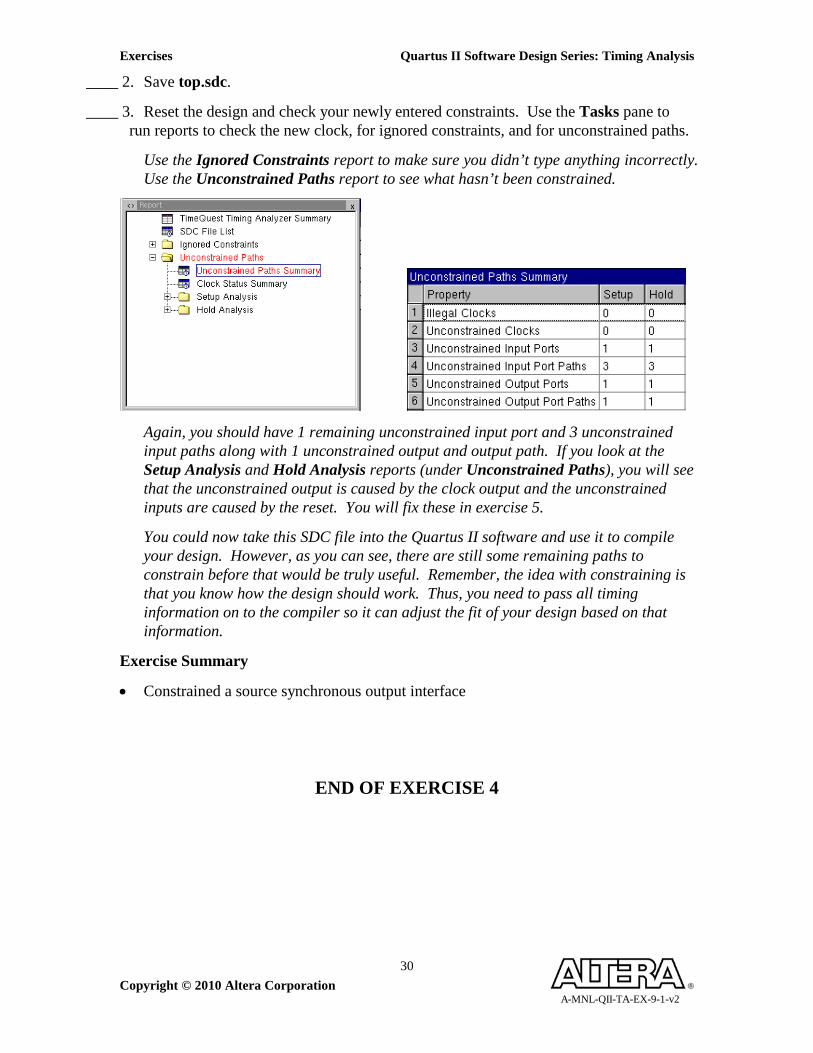
____ 4. Reset the design and check your newly entered constraints. Use the Tasks pane to run reports to check the new clock, for ignored constraints, and for unconstrained paths.
Use the Ignored Constraints report to make sure you didn’t type anything incorrectly. Use the Unconstrained Paths report to see what hasn’t been constrained.
Exercises Quartus II Software Design Series: Timing Analysis
Copyright © 2010 Altera Corporation A-MNL-QII-TA-EX-9-1-v2
26
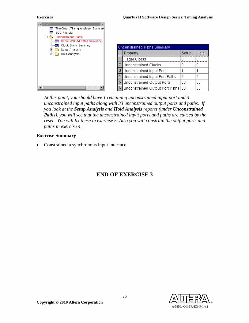
At this point, you should have 1 remaining unconstrained input port and 3 unconstrained input paths along with 33 unconstrained output ports and paths. If you look at the Setup Analysis and Hold Analysis reports (under Unconstrained Paths), you will see that the unconstrained input ports and paths are caused by the reset. You will fix these in exercise 5. Also you will constrain the output ports and paths in exercise 4.
Exercise Summary
• Constrained a synchronous input interface
END OF EXERCISE 3
Quartus II Software Design Series: Timing Analysis Exercises
Copyright © 2010 Altera Corporation A-MNL-QII-TA-EX-9-1-v2
27
Exercise 4
Timing Analysis: Source Synchronous Output
Constraints

Exercises Quartus II Software Design Series: Timing Analysis
Copyright © 2010 Altera Corporation A-MNL-QII-TA-EX-9-1-v2
28
Exercise 4
Objective:
• Constrain the source synchronous output paths in the design
Quartus II Software Design Series: Timing Analysis Exercises
Copyright © 2010 Altera Corporation A-MNL-QII-TA-EX-9-1-v2
29
Step 1: Constrain Source Synchronous Outnput paths using SDC
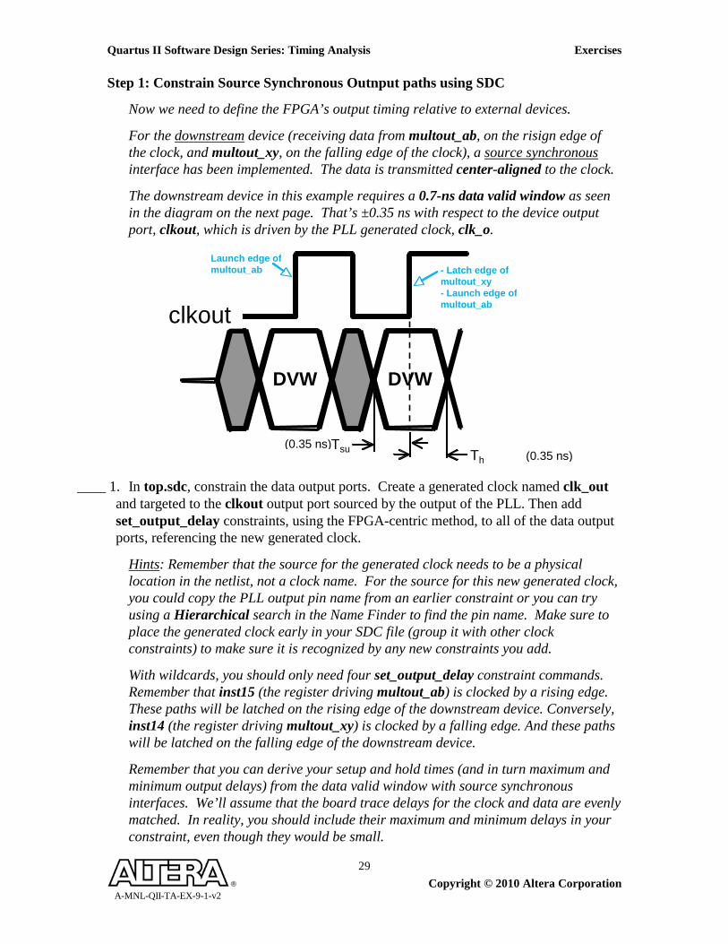
Now we need to define the FPGA’s output timing relative to external devices.
For the downstream device (receiving data from multout_ab, on the risign edge of the clock, and multout_xy, on the falling edge of the clock), a source synchronous interface has been implemented. The data is transmitted center-aligned to the clock.
The downstream device in this example requires a 0.7-ns data valid window as seen in the diagram on the next page. That’s ±0.35 ns with respect to the device output port, clkout, which is driven by the PLL generated clock, clk_o.
____ 1. In top.sdc, constrain the data output ports. Create a generated clock named clk_out and targeted to the clkout output port sourced by the output of the PLL. Then add set_output_delay constraints, using the FPGA-centric method, to all of the data output ports, referencing the new generated clock.
Hints: Remember that the source for the generated clock needs to be a physical location in the netlist, not a clock name. For the source for this new generated clock, you could copy the PLL output pin name from an earlier constraint or you can try using a Hierarchical search in the Name Finder to find the pin name. Make sure to place the generated clock early in your SDC file (group it with other clock constraints) to make sure it is recognized by any new constraints you add.
With wildcards, you should only need four set_output_delay constraint commands. Remember that inst15 (the register driving multout_ab) is clocked by a rising edge. These paths will be latched on the rising edge of the downstream device. Conversely, inst14 (the register driving multout_xy) is clocked by a falling edge. And these paths will be latched on the falling edge of the downstream device.
Remember that you can derive your setup and hold times (and in turn maximum and minimum output delays) from the data valid window with source synchronous interfaces. We’ll assume that the board trace delays for the clock and data are evenly matched. In reality, you should include their maximum and minimum delays in your constraint, even though they would be small.
DVW DVW
T su T h
Launch edge of multout_ab - Latch edge of
multout_xy - Launch edge of multout_ab
(0.35 ns) (0.35 ns)
clkout
Exercises Quartus II Software Design Series: Timing Analysis
Copyright © 2010 Altera Corporation A-MNL-QII-TA-EX-9-1-v2
30
____ 2. Save top.sdc.
____ 3. Reset the design and check your newly entered constraints. Use the Tasks pane to run reports to check the new clock, for ignored constraints, and for unconstrained paths.
Use the Ignored Constraints report to make sure you didn’t type anything incorrectly. Use the Unconstrained Paths report to see what hasn’t been constrained.
Again, you should have 1 remaining unconstrained input port and 3 unconstrained input paths along with 1 unconstrained output and output path. If you look at the Setup Analysis and Hold Analysis reports (under Unconstrained Paths), you will see that the unconstrained output is caused by the clock output and the unconstrained inputs are caused by the reset. You will fix these in exercise 5.
You could now take this SDC file into the Quartus II software and use it to compile your design. However, as you can see, there are still some remaining paths to constrain before that would be truly useful. Remember, the idea with constraining is that you know how the design should work. Thus, you need to pass all timing information on to the compiler so it can adjust the fit of your design based on that information.
Exercise Summary
• Constrained a source synchronous output interface
END OF EXERCISE 4
Quartus II Software Design Series: Timing Analysis Exercises
Copyright © 2010 Altera Corporation A-MNL-QII-TA-EX-9-1-v2
31
Exercise 5
Timing Analysis: Timing Exceptions &
Analysis

Exercises Quartus II Software Design Series: Timing Analysis
Copyright © 2010 Altera Corporation A-MNL-QII-TA-EX-9-1-v2
32
Quartus II Software Design Series: Timing Analysis Exercises
Copyright © 2010 Altera Corporation A-MNL-QII-TA-EX-9-1-v2
33
Exercise 5
Objectives:
• Constrain asynchronous input signals
• Eliminate timing violations by using timing exceptions
Exercises Quartus II Software Design Series: Timing Analysis
Copyright © 2010 Altera Corporation A-MNL-QII-TA-EX-9-1-v2
34
Step 1: Constrain asynchronous path
In this step, you will constrain the asynchronous input path of this design.
Look at the reset circuit in the design schematic. You can see that the design has a reset driven by an external source. Let’s assume the input path is truly asynchronous (no timing on the external path), so the solution to synchronize the reset internally is the correct one. The circuit shown is a common method of synchronizing a reset to your internal clock domain. Since this a truly asynchronous input and no external timing is known, a false path exception is needed to constrain the path.
____ 1. In top.sdc, use an SDC command to constrain all paths from the asynchronous reset input.
____ 2. Save top.sdc.
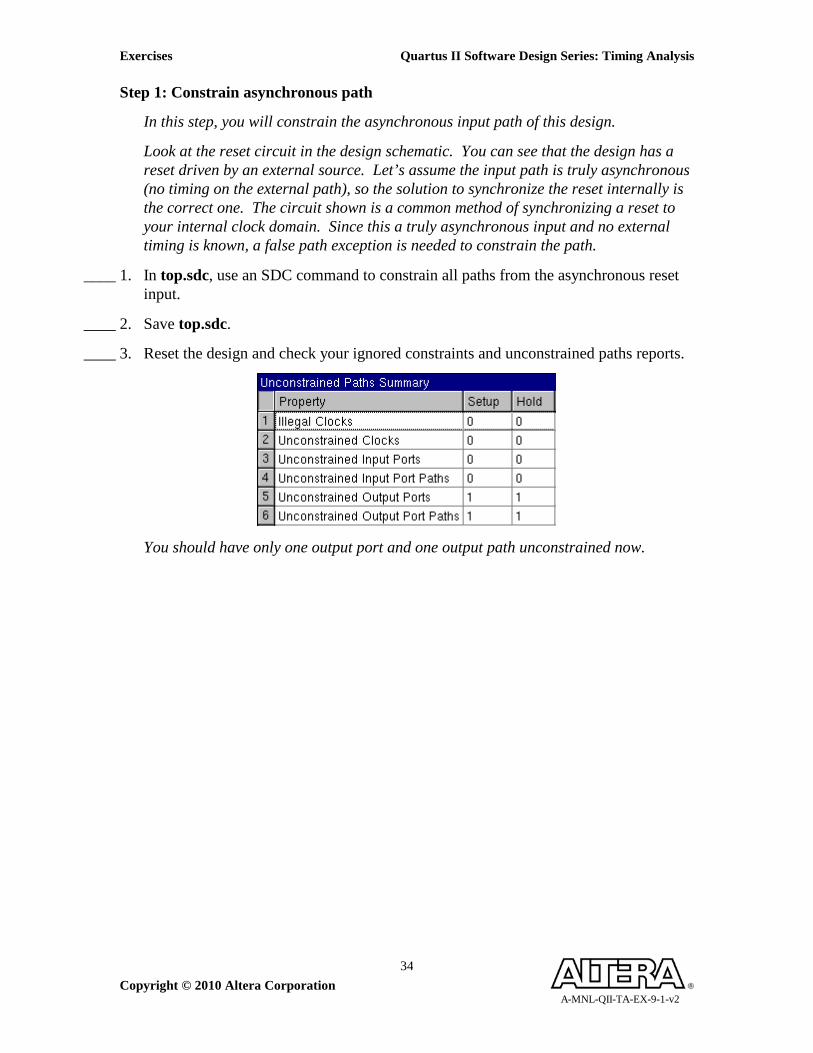
____ 3. Reset the design and check your ignored constraints and unconstrained paths reports.
You should have only one output port and one output path unconstrained now.
Quartus II Software Design Series: Timing Analysis Exercises
Copyright © 2010 Altera Corporation A-MNL-QII-TA-EX-9-1-v2
35
Step 2: Constrain clock output port
____ 1. In the Unconstrained Paths report folder, examine the Unconstrained Output Ports and Unconstrained Output Port Paths reports (expand the Setup Analysis or Hold Analysis folders).
You should see that the port clkout is the only unconstrained output. It appears as unconstrained because the timing analyzer has determined the path from the clock output of the PLL to the clkout port is an unconstrained combinatorial path. This path is considered as both a clock path (for the source synchronous interface) and a data path (any path that goes to an output port) thanks to the TimeQuest timing analyzer’s “clock as data” analysis feature. Remember that a “clock” in SDC is not a node. It refers to the behavior of a node in the design. Without TimeQuest’s clock-as-data analysis, besides clkout, clk_in would be considered an unconstrained input port, even with the create_clock constraint we created at the beginning of Exercise 2.
While the path from the PLL to clkout is actually a true combinatorial path in the design, it is a timing-based false path and does not need to be analyzed for timing. By design, you are only concerned with the relationship of the output clock to the output data and not with the absolute time between clk_o and clk_out.
____ 2. In top.sdc, use an SDC command to tell the TimeQuest timing analyzer not to analyze the path from the PLL output pin to the clock output port clkout.
Hint: Again, you could copy the pin name from an earlier constraint or you can try using a Hierarchical search in the Name Finder to find the pin name.
____ 3. Save top.sdc.
____ 4. Reset the design and check your ignored constraints and unconstrained paths reports.
All paths should now be constrained.
Exercises Quartus II Software Design Series: Timing Analysis
Copyright © 2010 Altera Corporation A-MNL-QII-TA-EX-9-1-v2
36
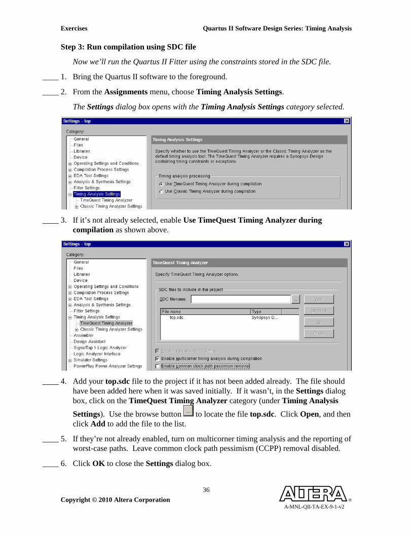
Step 3: Run compilation using SDC file
Now we’ll run the Quartus II Fitter using the constraints stored in the SDC file.
____ 1. Bring the Quartus II software to the foreground.
____ 2. From the Assignments menu, choose Timing Analysis Settings.
The Settings dialog box opens with the Timing Analysis Settings category selected.
____ 3. If it’s not already selected, enable Use TimeQuest Timing Analyzer during
compilation as shown above.
____ 4. Add your top.sdc file to the project if it has not been added already. The file should
have been added here when it was saved initially. If it wasn’t, in the Settings dialog box, click on the TimeQuest Timing Analyzer category (under Timing Analysis
Settings). Use the browse button to locate the file top.sdc. Click Open, and then click Add to add the file to the list.
____ 5. If they’re not already enabled, turn on multicorner timing analysis and the reporting of worst-case paths. Leave common clock path pessimism (CCPP) removal disabled.
____ 6. Click OK to close the Settings dialog box.
Quartus II Software Design Series: Timing Analysis Exercises
Copyright © 2010 Altera Corporation A-MNL-QII-TA-EX-9-1-v2
37
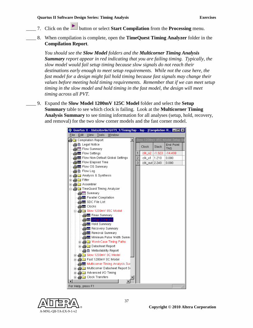
____ 7. Click on the button or select Start Compilation from the Processing menu.
____ 8. When compilation is complete, open the TimeQuest Timing Analyzer folder in the Compilation Report.
You should see the Slow Model folders and the Multicorner Timing Analysis Summary report appear in red indicating that you are failing timing. Typically, the slow model would fail setup timing because slow signals do not reach their destinations early enough to meet setup requirements. While not the case here, the fast model for a design might fail hold timing because fast signals may change their values before meeting hold timing requirements. Remember that if we can meet setup timing in the slow model and hold timing in the fast model, the design will meet timing across all PVT.
____ 9. Expand the Slow Model 1200mV 125C Model folder and select the Setup Summary table to see which clock is failing. Look at the Multicorner Timing Analysis Summary to see timing information for all analyses (setup, hold, recovery, and removal) for the two slow corner models and the fast corner model.
Exercises Quartus II Software Design Series: Timing Analysis
Copyright © 2010 Altera Corporation A-MNL-QII-TA-EX-9-1-v2
38
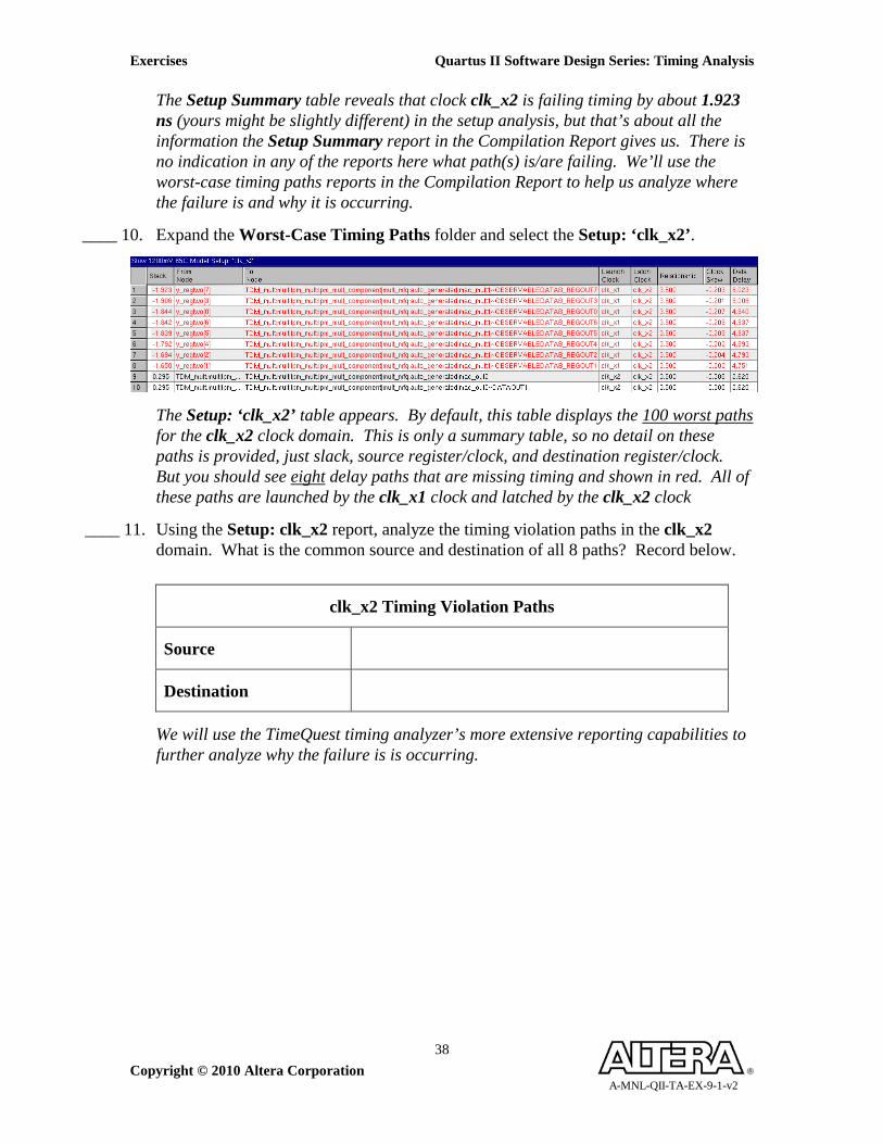
The Setup Summary table reveals that clock clk_x2 is failing timing by about 1.923 ns (yours might be slightly different) in the setup analysis, but that’s about all the information the Setup Summary report in the Compilation Report gives us. There is no indication in any of the reports here what path(s) is/are failing. We’ll use the worst-case timing paths reports in the Compilation Report to help us analyze where the failure is and why it is occurring.
____ 10. Expand the Worst-Case Timing Paths folder and select the Setup: ‘clk_x2’.
The Setup: ‘clk_x2’ table appears. By default, this table displays the 100 worst paths for the clk_x2 clock domain. This is only a summary table, so no detail on these paths is provided, just slack, source register/clock, and destination register/clock. But you should see eight delay paths that are missing timing and shown in red. All of these paths are launched by the clk_x1 clock and latched by the clk_x2 clock
____ 11. Using the Setup: clk_x2 report, analyze the timing violation paths in the clk_x2 domain. What is the common source and destination of all 8 paths? Record below.
clk_x2 Timing Violation Paths
Source
Destination
We will use the TimeQuest timing analyzer’s more extensive reporting capabilities to further analyze why the failure is is occurring.
Quartus II Software Design Series: Timing Analysis Exercises
Copyright © 2010 Altera Corporation A-MNL-QII-TA-EX-9-1-v2
39
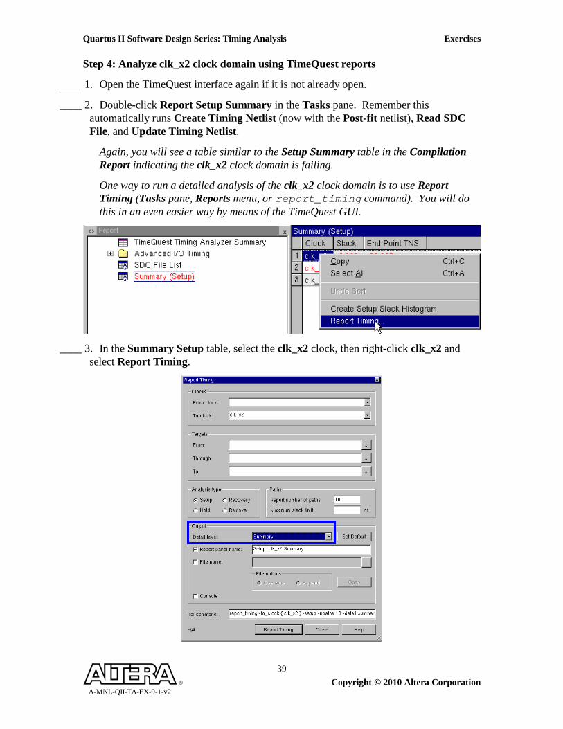
Step 4: Analyze clk_x2 clock domain using TimeQuest reports
____ 1. Open the TimeQuest interface again if it is not already open.
____ 2. Double-click Report Setup Summary in the Tasks pane. Remember this automatically runs Create Timing Netlist (now with the Post-fit netlist), Read SDC File, and Update Timing Netlist.
Again, you will see a table similar to the Setup Summary table in the Compilation Report indicating the clk_x2 clock domain is failing.
One way to run a detailed analysis of the clk_x2 clock domain is to use Report Timing (Tasks pane, Reports menu, or report_timing command). You will do this in an even easier way by means of the TimeQuest GUI.
____ 3. In the Summary Setup table, select the clk_x2 clock, then right-click clk_x2 and
select Report Timing.
Exercises Quartus II Software Design Series: Timing Analysis
Copyright © 2010 Altera Corporation A-MNL-QII-TA-EX-9-1-v2
40
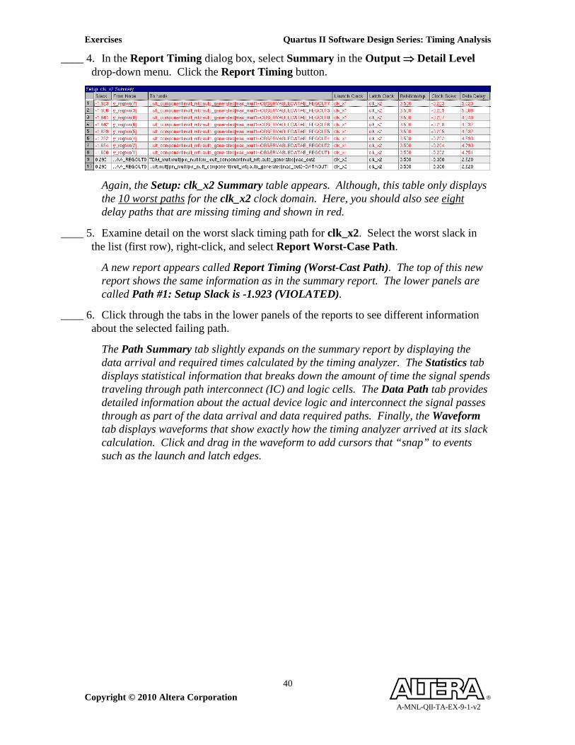
____ 4. In the Report Timing dialog box, select Summary in the Output ⇒ Detail Level drop-down menu. Click the Report Timing button.
Again, the Setup: clk_x2 Summary table appears. Although, this table only displays the 10 worst paths for the clk_x2 clock domain. Here, you should also see eight delay paths that are missing timing and shown in red.
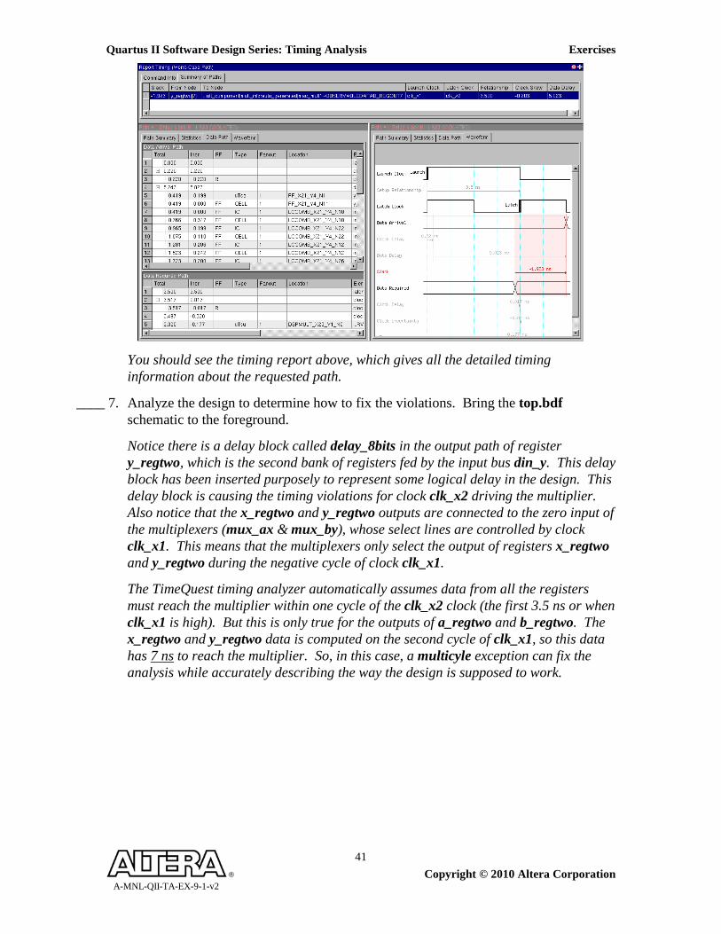
____ 5. Examine detail on the worst slack timing path for clk_x2. Select the worst slack in the list (first row), right-click, and select Report Worst-Case Path.
A new report appears called Report Timing (Worst-Cast Path). The top of this new report shows the same information as in the summary report. The lower panels are called Path #1: Setup Slack is -1.923 (VIOLATED).
____ 6. Click through the tabs in the lower panels of the reports to see different information about the selected failing path.
The Path Summary tab slightly expands on the summary report by displaying the data arrival and required times calculated by the timing analyzer. The Statistics tab displays statistical information that breaks down the amount of time the signal spends traveling through path interconnect (IC) and logic cells. The Data Path tab provides detailed information about the actual device logic and interconnect the signal passes through as part of the data arrival and data required paths. Finally, the Waveform tab displays waveforms that show exactly how the timing analyzer arrived at its slack calculation. Click and drag in the waveform to add cursors that “snap” to events such as the launch and latch edges.
Quartus II Software Design Series: Timing Analysis Exercises
Copyright © 2010 Altera Corporation A-MNL-QII-TA-EX-9-1-v2
41
You should see the timing report above, which gives all the detailed timing information about the requested path.
____ 7. Analyze the design to determine how to fix the violations. Bring the top.bdf schematic to the foreground.
Notice there is a delay block called delay_8bits in the output path of register y_regtwo, which is the second bank of registers fed by the input bus din_y. This delay block has been inserted purposely to represent some logical delay in the design. This delay block is causing the timing violations for clock clk_x2 driving the multiplier. Also notice that the x_regtwo and y_regtwo outputs are connected to the zero input of the multiplexers (mux_ax & mux_by), whose select lines are controlled by clock clk_x1. This means that the multiplexers only select the output of registers x_regtwo and y_regtwo during the negative cycle of clock clk_x1.
The TimeQuest timing analyzer automatically assumes data from all the registers must reach the multiplier within one cycle of the clk_x2 clock (the first 3.5 ns or when clk_x1 is high). But this is only true for the outputs of a_regtwo and b_regtwo. The x_regtwo and y_regtwo data is computed on the second cycle of clk_x1, so this data has 7 ns to reach the multiplier. So, in this case, a multicyle exception can fix the analysis while accurately describing the way the design is supposed to work.
Exercises Quartus II Software Design Series: Timing Analysis
Copyright © 2010 Altera Corporation A-MNL-QII-TA-EX-9-1-v2
42
Step 5: Use multi-cycle constraints to correct failing internal paths
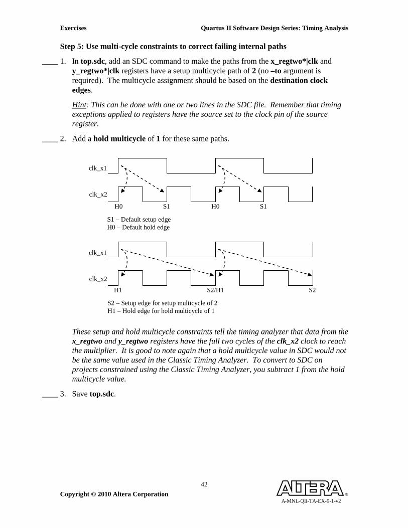
____ 1. In top.sdc, add an SDC command to make the paths from the x_regtwo*|clk and y_regtwo*|clk registers have a setup multicycle path of 2 (no –to argument is required). The multicycle assignment should be based on the destination clock edges.
Hint: This can be done with one or two lines in the SDC file. Remember that timing exceptions applied to registers have the source set to the clock pin of the source register.
____ 2. Add a hold multicycle of 1 for these same paths.
These setup and hold multicycle constraints tell the timing analyzer that data from the x_regtwo and y_regtwo registers have the full two cycles of the clk_x2 clock to reach the multiplier. It is good to note again that a hold multicycle value in SDC would not be the same value used in the Classic Timing Analyzer. To convert to SDC on projects constrained using the Classic Timing Analyzer, you subtract 1 from the hold multicycle value.
____ 3. Save top.sdc.
S1 – Default setup edge H0 – Default hold edge
S1 H0 S1 H0
S2 – Setup edge for setup multicycle of 2 H1 – Hold edge for hold multicycle of 1
H1 S2 S2/H1
clk_x1
clk_x2
clk_x1
clk_x2
Quartus II Software Design Series: Timing Analysis Exercises
Copyright © 2010 Altera Corporation A-MNL-QII-TA-EX-9-1-v2
43
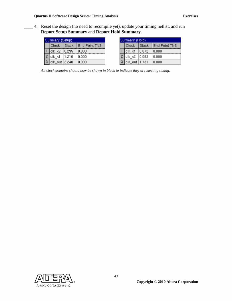
____ 4. Reset the design (no need to recompile yet), update your timing netlist, and run Report Setup Summary and Report Hold Summary.
All clock domains should now be shown in black to indicate they are meeting timing.
Exercises Quartus II Software Design Series: Timing Analysis
Copyright © 2010 Altera Corporation A-MNL-QII-TA-EX-9-1-v2
44
Step 6: Analyze asynchronous timing in the design
____ 1. From the Tasks pane, generate the recovery and removal summary reports.
You should see only positive slack on all asynchronous signals in the design. The summary reports indicate that all asynchronous signals are within the clk_x1 clock domain. Let’s examine the asynchronous paths in more detail.
____ 2. In the Summary (Recovery) report, select and right-click clk_x1, and select Report Timing.
____ 3. Set the report Detail level to Path Only, and set the number of paths to analyze to 100. Click Report Timing.
____ 4. Scroll to the bottom of the summary report and note the number of paths reported. What is the common source for all these paths? Check the schematic to find this instance in the design.
Notice that this is the second register of the reset synchronization circuit that generates the aclr signal. Since this signal connects to the asynchronous reset pins of 96 registers in the design, 96 paths are listed in the report. The input reset signal is also asynchronous, but since we set reset to be a false path, it does not get analyzed or included in the report.
Note that both the launch and latch clocks for all 96 paths is the clk_x1 clock. Remember that the recovery analysis is analogous to the setup analysis of synchronous signals and removal analysis is analogous to hold. Since this asynchronous signal is synchronized into the clk_x1 clock domain, clk_x1 is the clock indicated in the recovery and removal summary reports.
____ 5. Close TimeQuest Timing Analyzer.
____ 6. Recompile the design in the Quartus II software.
Quartus II Software Design Series: Timing Analysis Exercises
Copyright © 2010 Altera Corporation A-MNL-QII-TA-EX-9-1-v2
45
Step 7: Use the PLL to center the data valid window
Though all timing constraints are being met, typically you want to center your actual data valid window around your output clock, in this case clk_out. Notice from the setup and hold summary reports that the setup slack for clk_out is much bigger than the hold slack. This means that the data valid window is skewed with respect to the data required window. To fix this, you will adjust the PLL to shift the clk_o clock.
____ 1. In the table below, under Slow Analysis, record the slack values for clk_out from the Setup Summary and Hold Summary reports from the Slow Models in the Quartus II compilation report.
Make sure you look through both slow corner reports in the Quartus II compilation report. Of the two setup slacks, record the larger one. Of the two hold slacks, record the smaller one.
Slow Analysis Fast Analysis
Setup Slack Hold Slack Setup Slack Hold Slack
____ 2. In the table above, under Fast Analysis, record the slack values from the Fast corner Setup Summary and Hold Summary reports for clk_out.
To figure out how much the PLL output clock clk_o needs to be shifted, we need to find the center of the data valid window. The fast and slow models give you the absolute smallest slack for both corner cases. Now, if you subtract the smallest setup slack value in the table (from either the fast or slow analyses) from the smallest hold slack value from either analysis and divide the result by 2, you can find this center. Round the calculated value to the nearest hundredth (2 decimal places).
(SMALLEST HOLD VALUE – SMALLEST SETUP SLACK) ÷ 2 = ___________
____ 3. Add this time shift on the c2 output of the PLL. Bring the top.bdf schematic to the foreground. Double-click the PLL block in the schematic. In the MegaWizard Plug-In Manager, go to page 6 (clk c2 of the Output Clocks section). In the Clock phase shift field, enter the rounded time delay shift you calculated above (with the negative sign) and change the units to ns. The MegaWizard indicates what the actual shift will be, which may be slightly different from your entered value. Click Finish twice and then click OK. You will also have to update the symbol.
NOTE: This may resize the PLL symbol in the diagram so make sure that all connections to it are still correct.
____ 4. From the PLL symbol in the schematic, note the equivalent phase shift in degrees that the MegaWizard Plug-In Manager has determined will give you your shift on the c2 output. Enter that value here (don’t forget the minus sign): _______ °
Exercises Quartus II Software Design Series: Timing Analysis
Copyright © 2010 Altera Corporation A-MNL-QII-TA-EX-9-1-v2
46
____ 5. In top.sdc, add the -phase argument to your generated clock statement for the clk_o (not clk_out) clock using the phase shift value from the PLL symbol (units are not required).
____ 6. Save top.sdc.
Before recompiling, you should lock down device I/O selected by the Fitter during the last compilation. This ensures that the Fitter does not select different locations for your I/O ports and thus possibly change your timing.
____ 7. Fix device I/O locations. From the Quartus II Assignments menu, select Back-Annotate Assignments. In the Back-Annotate Assignments dialog box, leave the defaults (Pin & device assignments). Click OK.
____ 8. Recompile the design, saving changes to the .bdf schematic file.
____ 9. Check timing. After compilation, re-open the timing analyzer and recheck your Summary (Setup) and Summary (Hold) reports. Check both the slow and fast netlists by just changing the operating conditions (Netlist menu, Set Operating Conditions) and regenerating the out of date reports. Enter the new values for clkout here:
Slow Analysis Fast Analysis
Setup Slack Hold Slack Setup Slack Hold Slack
Again, make sure you look through both slow corner reports in the Quartus II compilation report. Of the two setup slacks, record the larger one. Of the two hold slacks, record the smaller one. Now you should notice more of a balance between the slack times. This indicates that the data valid window is now centered around the clock and the data required times.
Exercise Summary
• Constrained an asynchronous control input
• Adding timing exceptions (i.e. false path and multicycle) to match design functionality
• Adjusted PLL settings to improve timing of a source synchronous interface
END OF EXERCISE 5