Embed Size (px)
Citation preview

CE
RN
-TH
ESIS
-2006-0
57
29/0
4/2
005
Detector Developments for the LHC:
CMS TOB Silicon Detector Modules and ATLAS TileCal Read-Out Driver
Research Report
Treball d’Investigació
Joaquín Poveda Torres
Departament de Física Atòmica, Molecular i Nuclear
Universitat de València
April 29th, 2005
Directors: Juan A. Valls Ferrer
Antonio Ferrer Soria

2

3
En ANTONIO FERRER SORIA, Catedràtic de la Universitat de València y membre del Departament de Física Atòmica, Molecular i Nuclear de la Facultat de Física de la Universitat de València i de l’Institut de Física Corpuscular (IFIC) de València.
CERTIFICA:
Que la present memòria “Detector Developments for the LHC: CMS TOB Silicon Detector Modules and ATLAS TileCal Read-Out Driver” ha sigut realitzada sota la meva direcció i la del Dr. JUAN ANTONIO VALLS FERRER en el Institut de Física Corpuscular (Centre Mixt Universitat de València – C.S.I.C.) per En JOAQUÍN POVEDA TORRES y constitueix el seu treball d’Investigació per a optar al Diploma d’Estudis Avançats (D.E.A)
I per a que conste, en compliment de la legislació vigent, firmem el present Certificat a 12 d’Abril de 2004.
Dr. Antonio Ferrer Soria Dr. Juan Antonio Valls Ferrer

4

5
Index
LAYOUT ...............................................................................................................................................................................15
INTRODUCTIONINTRODUCTIONINTRODUCTIONINTRODUCTION ............................................................................................................................................................17
1 CERN.............................................................................................................................................................................18
2 THE LARGE HADRON COLLIDER (LHC) .......................................................................................................20
3 EXPERIMENTS FOR THE LHC............................................................................................................................22
3.1 GENERAL STRUCTURE FOR PARTICLE PHYSICS EXPERIMENTS ...........................................................................22 3.2 COMPACT MUON SOLENOID (CMS).....................................................................................................................25 3.2.1 Inner Detector...............................................................................................................................................25 3.2.2 Electromagnetic Calorimetry: ECAL and Preshower...............................................................................27 3.2.3 Hadronic Calorimetry: HCAL....................................................................................................................28 3.2.4 Muon System.................................................................................................................................................29 3.2.5 Magnet System..............................................................................................................................................30
3.3 A TOROIDAL LHC APARATUS (ATLAS).............................................................................................................31 3.3.1 Inner Detector...............................................................................................................................................31 3.3.2 Calorimetry...................................................................................................................................................33
3.3.2.1 Liquid Argon Calorimeter .......................................................................................................................33 3.3.2.2 Tile Calorimeter (TileCal) .......................................................................................................................34
3.3.3 Muon System.................................................................................................................................................35 3.3.4 Magnet System..............................................................................................................................................37
PART 1: PERFORMANCE OF CMS TPERFORMANCE OF CMS TPERFORMANCE OF CMS TPERFORMANCE OF CMS TOB SILICON DETECTOR OB SILICON DETECTOR OB SILICON DETECTOR OB SILICON DETECTOR MODULES ON A DOUBLE MODULES ON A DOUBLE MODULES ON A DOUBLE MODULES ON A DOUBLE
SIDED PROTOTYPE RODSIDED PROTOTYPE RODSIDED PROTOTYPE RODSIDED PROTOTYPE ROD .........................................................................................................................................39
4 INTRODUCTION.......................................................................................................................................................40
4.1 SILICON DETECTOR MODULES DESCRIPTION.......................................................................................................40 4.2 READ-OUT ELECTRONICS ......................................................................................................................................40 4.3 ROD DESCRIPTION .................................................................................................................................................41 4.4 MOTIVATION..........................................................................................................................................................42
5 SYSTEM TEST SETUP.............................................................................................................................................42
6 NOISE ANALYSIS .....................................................................................................................................................43
6.1 DEFINITIONS...........................................................................................................................................................43 6.2 RESULTS.................................................................................................................................................................44 6.2.1 Pedestals .......................................................................................................................................................44 6.2.2 Noise..............................................................................................................................................................44 6.2.3 Common Mode Noise...................................................................................................................................47
6.3 BAD STRIPS DEFINITION........................................................................................................................................48
7 SIGNAL ANALYSIS ..................................................................................................................................................48
7.1 CLUSTER ALGORITHMS AND CLUSTER THRESHOLDS..........................................................................................49 7.2 RESULTS.................................................................................................................................................................51 7.2.1 Gaussian-Landau Convolution Fit ..............................................................................................................51
8 NOISE OCCUPANCY ...............................................................................................................................................57
8.1 DEFINITION ............................................................................................................................................................57 8.2 RESULTS.................................................................................................................................................................57
9 SIGNAL EFFICIENCY .............................................................................................................................................57

6
9.1 DEFINITION ............................................................................................................................................................57 9.2 RESULTS.................................................................................................................................................................58
10 SIGNAL EFFICIENCY VS NOISE OCCUPANCY ........................................................................................60
REFERENCES ON PART 1 ..............................................................................................................................................64
PART 2: STANDALONE SOFTWARE STANDALONE SOFTWARE STANDALONE SOFTWARE STANDALONE SOFTWARE FOR ATLAS TILECAL ROFOR ATLAS TILECAL ROFOR ATLAS TILECAL ROFOR ATLAS TILECAL ROD CHARACTERIZATION D CHARACTERIZATION D CHARACTERIZATION D CHARACTERIZATION
AND SYSTEM TESTSAND SYSTEM TESTSAND SYSTEM TESTSAND SYSTEM TESTS..................................................................................................................................................67
11 INTRODUCTION ..................................................................................................................................................68
11.1 TILECAL FRONT-END ELECTRONICS ....................................................................................................................68 11.1.1 PMT Block ....................................................................................................................................................68
11.1.1.1 Photomultipliers...................................................................................................................................69 11.1.1.2 Light Mixers.........................................................................................................................................69 11.1.1.3 Magentic shielding...............................................................................................................................70 11.1.1.4 HV Dividers.........................................................................................................................................70 11.1.1.5 3-in-1 Boards........................................................................................................................................70
11.1.2 Digitizer System............................................................................................................................................70 11.1.3 Digitizer-to-Slink Interface Links.................................................................................................................71
11.2 TILECAL BACK-END ELECTRONICS: ROD CRATE ..............................................................................................71 11.2.1 Overview Set-up............................................................................................................................................71
11.2.1.1 Crate Controller ...................................................................................................................................73 11.2.1.2 Trigger and Busy Module (TBM).......................................................................................................73 11.2.1.3 ROD Motherboard...............................................................................................................................73 11.2.1.4 Transition Module ...............................................................................................................................73
11.2.2 ROD Description..........................................................................................................................................74 11.2.2.1 Optical receivers and G-link chips......................................................................................................74 11.2.2.2 Staging FPGAs ....................................................................................................................................75 11.2.2.3 Output Controller FPGAs....................................................................................................................75 11.2.2.4 VME FPGA.........................................................................................................................................75 11.2.2.5 TTC Controller FPGA.........................................................................................................................75 11.2.2.6 Processing Units ..................................................................................................................................76
11.2.2.6.1 FPGA PU.........................................................................................................................................76 11.2.2.6.2 DSP PU............................................................................................................................................76
11.2.3 Installation for ATLAS..................................................................................................................................77 11.2.4 System Test Setups........................................................................................................................................79
12 STANDALONE SOFTWARE FOR ROD TESTS ...........................................................................................79
13 INSTALLATION AND SETUP ...........................................................................................................................79
14 SOFTWARE DEVELOPMENT..........................................................................................................................80
15 USING XTESTROD...............................................................................................................................................82
15.1 THE VMEBUS MENU.............................................................................................................................................84 15.2 THE TTCVI MENU .................................................................................................................................................85 15.2.1 TTCvi L1A Trigger.......................................................................................................................................85 15.2.2 Bunch Crossing and Orbit Register.............................................................................................................86 15.2.3 Event/Orbit Counter Register ......................................................................................................................86 15.2.4 B-Go Channels .............................................................................................................................................86
15.3 THE ROD FINAL MENU.........................................................................................................................................86 15.3.1 VME Controller............................................................................................................................................87
15.3.1.1 Local Register ......................................................................................................................................88 15.3.1.2 IRQ Registers.......................................................................................................................................88
15.3.2 Busy Registers...............................................................................................................................................88 15.3.2.1 Miscellaneous Register........................................................................................................................88 15.3.2.2 Status Register......................................................................................................................................90 15.3.2.3 Timing counters ...................................................................................................................................90

7
15.3.3 Output Controller .........................................................................................................................................90 15.3.3.1 Configuration Register ........................................................................................................................90 15.3.3.2 Status Register......................................................................................................................................92 15.3.3.3 SDRAM Register.................................................................................................................................92 15.3.3.4 Dummy Register..................................................................................................................................92 15.3.3.5 Version Register ..................................................................................................................................92
15.3.4 TTC Controller FPGA .................................................................................................................................92 15.3.4.1 Control Register...................................................................................................................................92 15.3.4.2 Status Register......................................................................................................................................93 15.3.4.3 Dummy Register..................................................................................................................................93 15.3.4.4 Version Register ..................................................................................................................................94
15.3.5 Staging FPGA...............................................................................................................................................94 15.3.5.1 Configuration Registers.......................................................................................................................96 15.3.5.2 RAM Data Transmission Registers ....................................................................................................96 15.3.5.3 Link Configuration Registers..............................................................................................................97 15.3.5.4 Status Register......................................................................................................................................97 15.3.5.5 Temperature Registers.........................................................................................................................97 15.3.5.6 Dummy Register..................................................................................................................................97 15.3.5.7 Version Register ..................................................................................................................................97
15.3.6 FPGA PU......................................................................................................................................................97 15.3.6.1 Data Format Registers .........................................................................................................................98 15.3.6.2 Configuration Register ......................................................................................................................100 15.3.6.3 Pulse and Set/Reset Busy Register....................................................................................................100 15.3.6.4 Status Register....................................................................................................................................100 15.3.6.5 Read Internal FIFO............................................................................................................................101 15.3.6.6 G-Link counters .................................................................................................................................101 15.3.6.7 Dummy Register................................................................................................................................101 15.3.6.8 Version Register ................................................................................................................................101
15.3.7 DSP PU.......................................................................................................................................................101 15.3.7.1 DSP Booting submenu ......................................................................................................................101 15.3.7.2 Output FPGA submenu.....................................................................................................................102 15.3.7.2.1 HPI Register ..................................................................................................................................102 15.3.7.2.2 McBSP2 Serial Data Register.......................................................................................................102 15.3.7.2.3 Control Register.............................................................................................................................102 15.3.7.2.4 Status Register ...............................................................................................................................103 15.3.7.2.5 Dummy Register ............................................................................................................................103 15.3.7.2.6 Version Register.............................................................................................................................103
15.3.7.3 Input FPGA submenu........................................................................................................................103 15.3.7.3.1 Configuration/Status Register.......................................................................................................104 15.3.7.3.2 Programming Register ..................................................................................................................104 15.3.7.3.3 Version Register.............................................................................................................................104
15.4 THE DAQ MENU .................................................................................................................................................104 15.4.1 Data Runs submenu....................................................................................................................................104
15.4.1.1 ROD Final PU – VME test mode......................................................................................................105 15.4.1.2 ROD Final PU – S-Link test mode....................................................................................................106
15.4.2 Temperature Runs submenu.......................................................................................................................106
16 USING XFILAR....................................................................................................................................................108
16.1 THE FILAR MENU...............................................................................................................................................110 16.2 THE DAQ MENU .................................................................................................................................................110
17 XTESTROD AND XFILAR PERFORMANCE .............................................................................................110
17.1 ROD PRE-PRODUCTION TESTS ...........................................................................................................................111 17.1.1 Output Data Flow Tests .............................................................................................................................111
17.1.1.1 Tests Paremeters ................................................................................................................................111 17.1.1.2 Results ................................................................................................................................................112
17.1.2 Full Input-Output Data Flow Tests ...........................................................................................................114 17.1.2.1 Test Paremeters..................................................................................................................................114 17.1.2.2 Results ................................................................................................................................................114
17.1.3 ROD G-Link Temperature Tests at Laboratory........................................................................................116

8
17.1.4 Debug During ROD Firmware Development...........................................................................................116 17.2 INTEGRATION AT THE COMBINED TEST BEAM SETUP........................................................................................116 17.3 PRE-ROD BOARD DEBUG AND DEVELOPMENT.................................................................................................117
REFERENCES ON PART 2 ............................................................................................................................................120
CONCLUSIONSCONCLUSIONSCONCLUSIONSCONCLUSIONS.............................................................................................................................................................123
18 CONCLUSIONS ...................................................................................................................................................125
APPENDIX I: ACRONYM LIST...................................................................................................................................129
APPENDIX II: FROM STANDARD MODEL PHYSICS TO LHC. A BRIEF REVIEW OF HIGH ENERGY
PHYSICS IN THE LAST YEARS AND THE NEAREST FUTURE.......................................................................133
APPENDIX III: DEFINITION OF SOME PHYSICAL MAGNITUDES..............................................................135
ACKNOLEDGEMENTS..................................................................................................................................................137

9
Figures
FIGURE 1: SCHEME (NOT TO SCALE) OF THE CERN ACCELERATOR FACILITIES. NOTE THE BEAM LINES FOR ISOLDE AND
CNGS. ............................................................................................................................................................................19 FIGURE 2: ON THE LEFT, SIMULATION OF THE LHC IN THE TUNNEL. ON THE RIGHT, PICTURE OF THE DIPOLE MAGNET FOR
THE LHC.........................................................................................................................................................................21 FIGURE 3: SITUATION OF THE 4 EXPERIMENTS IN THE LHC IN THE ACCELERATOR..............................................................21 FIGURE 4: DRAWING OF THE ALICE EXPERIMENT FOR THE LHC. .......................................................................................22 FIGURE 5: SCHEME OF THE LHCB EXPERIMENT FOR THE LHC.............................................................................................22 FIGURE 6: SCHEME OF A TYPICAL PARTICLE DETECTOR (TRANSVERSE VIEW) FOR COLLIDING BEAM EXPERIMENTS. NOTE
THE DIFFERENT PARTS AND THE BEHAVIOUR OF THE DIFFERENT TYPES OF PARTICLES INSIDE THE DETECTOR. .........23 FIGURE 7: THREE-DIMENSIONAL VIEW OF THE SUBDETECTORS IN CMS. NOTE THE ENDCAPS SHOWN IN THE LOWER LEFT
CORNER. ..........................................................................................................................................................................25 FIGURE 8: AXIAL VIEW OF CMS. THE DIFFERENT SUBDETECTORS AND THE TRACK OF A MUON IN THE MAGNETIC FIELD
ARE DISPLAYED...............................................................................................................................................................26 FIGURE 9: DRAWING OF THE SILICON PIXEL DETECTOR, WHERE THE TWO LAYERS IN THE CENTRAL REGION AND THE
ENDCAP DISKS CAN BE SEEN. ..........................................................................................................................................26 FIGURE 10: ON THE LEFT, AXIAL VIEW OF THE DIFFERENT PARTS OF THE TRACKER SYSTEM IN THE BARREL REGION. ON
THE RIGHT, THREE-DIMENSIONAL LAYOUT OF THE CMS TRACKING DETECTORS, WHERE THE DIFFERENT PARTS
MENTIONED IN THE TEXT CAN BE OBSERVED.................................................................................................................27 FIGURE 11: ON THE LEFT, PICTURE OF ONE OF THE CRYSTALS TO BE USED IN THE ECAL BARREL WITH ITS PHOTODIODES.
ON THE RIGHT, THREE-DIMENSIONAL VIEW OF THE ELECTROMAGNETIC CALORIMETER. ...........................................27 FIGURE 12: SCHEMATIC VIEW OF AN EVENT IN THE PRESHOWER DETECTOR........................................................................28 FIGURE 13: SCHEMATIC VIEW OF ONE QUADRANT OF THE ELECTROMAGNETIC AND HADRONIC CALORIMETRY AND THE
TRACKING SYSTEM INSIDE THE SOLENOID COIL, WHERE THE DIFFERENT PARTS OF THE DETECTORS CAN BE SEEN....29 FIGURE 14: SCHEMATIC VIEW OF THE DIFFERENT MUON DETECTORS AND THEIR EMPLACEMENT IN CMS. .......................29 FIGURE 15: THREE-DIMENSIONAL VIEW OF THE ATLAS DETECTOR. ...................................................................................31 FIGURE 16: THREE-DIMENSIONAL VIEW OF THE INNER DETECTOR WITH ALL THE SUBDETECTORS ARE LABELLED. .........32 FIGURE 17 : TRT BARREL AND ENDCAPS STRAWS. ................................................................................................................32 FIGURE 18: SCHEME OF THE CALORIMETERS IN ATLAS.......................................................................................................33 FIGURE 19: THREE-DIMENSIONAL VIEW OF THE LAR CALORIMETERS..................................................................................34 FIGURE 20: THREE-DIMENSIONAL VIEW OF THE TILECALORIMETER....................................................................................35 FIGURE 21: PRINCIPLE OF THE TILECAL DESIGN....................................................................................................................35 FIGURE 22: LAYOUT OF THE CELLS OF THE TILECAL BARREL (LEFT) AND EXTENDED BARREL (RIGHT) MODULES...........35 FIGURE 23: THREE-DIMENSIONAL VIEW OF THE MUON SPECTROMETER INSTRUMENTATION INDICATING THE AREAS
COVERED BY THE FOUR DIFFERENT CHAMBER TECHNOLOGIES. ...................................................................................36 FIGURE 24: TWO-DIMENSIONAL VIEW IN THE XY DIRECTION OF THE MUON SPECTROMETER SYSTEM. NOTE THE
DISTRIBUTION OF THE FOUR CHAMBER TECHNOLOGIES USED. .....................................................................................36 FIGURE 25 : ATLAS MAGNET SYSTEM SCHEME (ON THE LEFT) AND SIMULATION (ON THE RIGHT). NOTE THE CENTRAL
SOLENOID AND THE THREE TOROIDS. .............................................................................................................................37 FIGURE 26: SKETCH OF THE CMS TRACKER LAYOUT (A QUARTER OF THE Z VIEW, WITHOUT THE PIXEL DETECTOR). GREY
LINES REPRESENT SINGLE MODULES AND BLUE LINES DOUBLE MODULES. SEE ALSO FIGURE 10. ..............................40 FIGURE 27: PICTURE OF A DETECTOR MODULE. NOTE THE TWO WAFERS AND THE FOUR APVS.........................................41 FIGURE 28: PICTURE OF A ROD WITHOUT THE SILICON DETECTOR MODULES. ......................................................................42 FIGURE 29: MEAN PEDESTAL VALUES (IN ADC COUNTS) AS A FUNCTION OF CHANNEL NUMBER FOR MODULES 4 (TOP)
AND 5 (BOTTOM) IN DECONVOLUTION MODE (LEFT) AND PEAK MODE (RIGHT). FOUR BLOCKS OF 128 CHANNELS PER
APV ARE CLEARLY SEEN IN ALL PLOTS. ........................................................................................................................45 FIGURE 30 : NOISE VALUES (IN ADC COUNTS) AS A FUNCTION OF STRIP NUMBER FOR MODULES 4 (TOP) AND 5 (BOTTOM).
DATA HAS BEEN TAKEN IN DECONVOLUTION MODE. ....................................................................................................46 FIGURE 31 : NOISE VALUES (IN ADC COUNTS) AS A FUNCTION OF STRIP NUMBER FOR MODULES 4 (TOP) AND 5 (BOTTOM).
DATA HAS BEEN TAKEN IN PEAK MODE. ........................................................................................................................46 FIGURE 32: CMN DISTRIBUTIONS PER APV (IN ADC COUNTS) FOR MODULES 4 (TOP) AND 5 (BOTTOM). ALL DATA
SHOWN CORRESPONDS TO DECONVOLUTION MODE WITH INVERTERS ON (SOLID HISTOGRAMS) AND OFF (DASHED
HISTOGRAMS)..................................................................................................................................................................47 FIGURE 33: PLACEMENT OF THE BETA SOURCE RELATIVE TO THE POSITION OF THE SILICON MODULES IN THE DOUBLE-
SIDED ROD. ALL SOURCE AND COSMIC DATA SHOWN CORRESPOND TO THIS SETUP. ...................................................49
10
FIGURE 34: CLUSTER MULTIPLICITY PER EVENT FOR MODULES 4 (LEFT) AND 5 (RIGHT) FROM THE BETA SOURCE RUNS
(TOP) AND COSMIC RAY DATA (BOTTOM) ALWAYS IN DECONVOLUTION MODE...........................................................49 FIGURE 35: STRIP MULTIPLICITY FOR MODULE 4 (LEFT) AND 5 (RIGHT) FROM BETA SOURCE RUNS (TOP) AND COSMIC
DATA (BOTTOM) ALWAYS IN DECONVOLUTION MODE. .................................................................................................50 FIGURE 36: EXAMPLE OF A CLUSTER FOUND WITH THE ALGORITHM EMPLOYED. THE GREY AREA IS IDENTIFIED AS A
CLUSTER WITH THREE STRIPS: A SEED STRIP WITH S/N>5 AND TWO ADJACENT STRIPS WITH S/N>2..........................50 FIGURE 37: CLUSTER CHARGE DISTRIBUTION (IN ADC COUNTS) FOR SILICON MODULE 4 (PEAK MODE) WITH DEFAULT
SETTINGS FOR THE CLUSTER ALGORITHM EMPLOYED. THE FIRST PEAK CORRESPONDS TO NOISE CLUSTERS
FLUCTUATIONS. ..............................................................................................................................................................50 FIGURE 38: FIT RESULTS FOR THE SEED SIGNAL CHARGE DISTRIBUTIONS FOR MODULES 4 (LEFT) AND 5 (RIGHT). RESULTS
ARE SHOWN FOR BOTH THE SOURCE DATA (PEAK AND DECONVOLUTION) AND COSMIC DATA (DECONVOLUTION
ONLY). .............................................................................................................................................................................53 FIGURE 39: FIT RESULTS FOR THE S/N DISTRIBUTIONS (SEED CHARGE) FOR MODULES 4 (LEFT) AND 5 (RIGHT). RESULTS
ARE SHOWN FOR BOTH THE SOURCE DATA (PEAK AND DECONVOLUTION) AND COSMICS DATA (DECONVOLUTION
ONLY). .............................................................................................................................................................................54 FIGURE 40: FIT RESULTS FOR THE CLUSTER SIGNAL CHARGE DISTRIBUTIONS FOR MODULES 4 (LEFT) AND 5 (RIGHT).
RESULTS ARE SHOWN FOR BOTH THE SOURCE DATA (PEAK AND DECONVOLUTION) AND COSMIC DATA
(DECONVOLUTION ONLY). ..............................................................................................................................................55 FIGURE 41: FIT RESULTS FOR THE S/N DISTRIBUTIONS (THE SIGNAL CHARGE DISTRIBUTION IS CALCULATED AS THE
CLUSTER SIGNAL) FOR MODULES 4 (LEFT) AND 5 (RIGHT). RESULTS ARE SHOWN FOR BOTH THE SOURCE DATA (PEAK
AND DECONVOLUTION) AND COSMICS DATA (DECONVOLUTION ONLY).......................................................................56 FIGURE 42: NOISE OCCUPANCY AS A FUNCTION OF THRESHOLD LEVEL FOR MODULES 4 (LEFT) AND 5 (RIGHT). RESULTS
ARE SHOWN FOR DECONVOLUTION (TOP) AND PEAK MODE (BOTTOM). .......................................................................58 FIGURE 43: SIGNAL EFFICIENCY AS A FUNCTION OF THE THRESHOLD (IN ADC COUNTS) FOR MODULES 4 (LEFT) AND 5
(RIGHT). RESULTS ARE SHOWN FOR SOURCE AND COSMIC DATA AND FOR PEAK AND DECONVOLUTION MODES.......59 FIGURE 44: SIGNAL EFFICIENCY AS A FUNCTION OF NOISE OCCUPANCY FOR DIFFERENT THRESHOLD LEVELS. RESULTS
ARE SHOWN FOR MODULES 4 (BLACK POINTS) AND 5 (GREY POINTS) FROM BETA SOURCE DATA IN DECONVOLUTION
MODE. THE THRESHOLD IS THE SAME FOR ALL APVS OF THE MODULES AND IT IS VARIED FROM 10 TO 18 ADC
COUNTS ABOVE THE AVERAGE PEDESTAL OF THE CHIPS. ..............................................................................................61 FIGURE 45: SIGNAL EFFICIENCY AS A FUNCTION OF THE NOISE OCCUPANCY FOR DIFFERENT THRESHOLD LEVELS.
RESULTS ARE SHOWN FOR MODULES 4 (BLACK POINTS) AND 5 (GREY POINTS) FROM BETA SOURCE DATA IN PEAK
MODE. THE THRESHOLD IS THE SAME FOR ALL APVS OF THE MODULES AND IT IS VARIED FROM 8 TO 14 ADC
COUNTS ABOVE THE AVERAGE PEDESTAL OF THE CHIPS. ..............................................................................................62 FIGURE 46: SIGNAL EFFICIENCY AS A FUNCTION OF NOISE OCCUPANCY FOR THE DIFFERENT THRESHOLD LEVELS (IN ADC
COUNTS) FOR MODULES 4 (BLACK POINTS) AND 5 (GREY POINTS) FROM COSMIC RAY DATA IN DECONVOLUTION
MODE. THE THRESHOLD IS THE SAME FOR ALL APV OF THE MODULES AND IT IS VARIED FROM 10 TO 16 ADC
COUNTS ABOVE THE AVERAGE PEDESTAL OF THE CHIPS. ..............................................................................................63 FIGURE 47: ON THE LEFT, PICTURE OF A DRAWER INSIDE A GIRDER. ON THE RIGHT, DETAIL OF THE PMTS AND THE
ELECTRONIC IN THE DRAWER (TOP) AND SCHEME OF THE DRAWER INSIDE THE GIRDER, WITH ALL THE PARTS
LABELLED (BOTTOM)......................................................................................................................................................68 FIGURE 48: ON THE LEFT, ARRANGEMENT OF A PMT BLOCK. ON THE RIGHT, DETAIL PICTURES OF THE PHOTOMULTIPLIER
(TOP) AND THE 3-IN-1 BOARD (BOTTOM). ......................................................................................................................69 FIGURE 49: PICTURE OF THE OPTIC WLS FIBERS BUNDLES IN A TILECAL MODULE CONNECTED TO THE PMTS FOR THEIR
READ-OUT. ......................................................................................................................................................................69 FIGURE 50: DIGITIZER SYSTEM FOR A SINGLE CHANNEL. ......................................................................................................70 FIGURE 51: ON THE LEFT, DIGITIZERS MAP PER DRAWER IN A CB MODULE. ON THE RIGHT, PICTURE OF THE TILEDMU
CHIP. ................................................................................................................................................................................71 FIGURE 52: BLOCK DIAGRAM FOR THE INTERFACE CARD. NOTE THE REDUNDANT READ-OUT FROM THE INTERFACE CARD
TO THE ROD. ..................................................................................................................................................................71 FIGURE 53: SCHEME OF THE TILECAL PARTITIONS AND THE CORRESPONDING ROD CRATES. NOTE THE MODULES IN THE
ROD CRATE IN THE RIGHT-BOTTOM CORNER................................................................................................................72 FIGURE 54: VP110 CRATE CONTROLLER...............................................................................................................................73 FIGURE 55: TRIGGER AND BUSY MODULE (TBM). ...............................................................................................................73 FIGURE 56: ROD MOTHERBOARD...........................................................................................................................................74 FIGURE 57: TRANSITION MODULE...........................................................................................................................................74 FIGURE 58: LAYOUT OF THE ROD MOTHERBOARD. THE SOLID BLUE LINES INDICATE THE DATA FLOW; THE DASHED GREY
LINES, THE TTC INFORMATION AND THE SOLID GREY LINES, THE VME INTERFACE...................................................75 FIGURE 59: ROD DUMMY PROCESSING UNIT (OR FPGA PU). THE DEVICES WHICH FORM THE DUMMY PU ARE SHOWN
ON BLUE AND THE LEDS AND THEIR FUNCTIONALITY IN NORMAL MODE ARE SHOWN IN RED....................................77 FIGURE 60: PICTURE OF THE ROD DSP PU WITH ITS DEVICES LABELLED ...........................................................................77

11
FIGURE 61: ON THE LEFT, DRAWING OF THE UX15 AND USA15 ROOMS IN THE UNDERGROUND BUILDINGS FOR ATLAS.
ON THE RIGHT, DETAIL OF USA15, AND THE NUMBER OF RACKS THAT WILL BE PLACED IN EACH LEVEL. ................78 FIGURE 62: SCHEME OF THE 2 RACKS WHICH WILL HOLD THE ROD AND TTC CRATES. .....................................................78 FIGURE 63: XFILAR PROGRAM DEVELOPMENT USING GLADE. FROM LEFT TO RIGHT, THE GLADE MAIN WINDOW,
PROPERTY EDITOR, WIDGET TREE, WIDGET PALETTE AND XFILAR INTERFACE WINDOW CAN BE SEEN....................81 FIGURE 64: XTESTROD AND XFILAR CMT PACKAGES FILE STRUCTURE. ........................................................................81 FIGURE 65: XTESTROD MAIN WINDOW. NOTE THE HARDWARE STATUS SEMAPHORES IN THE UPPER PART OF THE WINDOW
(IN THIS CASE ONLY TTCVI AND ROD FINAL ARE ACTIVE)..........................................................................................83 FIGURE 66: XTESTROD SET OPTIONS WINDOW. ...................................................................................................................83 FIGURE 67: XTESTROD VMEBUS MENU. .............................................................................................................................84 FIGURE 68: XTESTROD TTCVI MENU...................................................................................................................................85 FIGURE 69: XTESTROD ROD FINAL VME CONTROLLER MENU. ..........................................................................................87 FIGURE 70: XTESTROD ROD FINAL BUSY REGISTERS MENU................................................................................................89 FIGURE 71: BUSY SCHEME LOGIC FOR THE ROD. ..................................................................................................................89 FIGURE 72: XTESTROD ROD FINAL OUTPUT CONTROLLER MENU. .....................................................................................91 FIGURE 73: SCHEME OF THE OC WORKING IN NORMAL MODE (LEFT) AND IN STAGING MODE (RIGHT). NOTE THE
DIFFERENT IN/OUT SETTING FOR THE TWO OCS WHEN WORKING IN STAGING MODE..................................................91 FIGURE 74: XTESTROD ROD FINAL TTC CONTROLLER MENU.............................................................................................93 FIGURE 75: SCHEME OF THE ROD WORKING IN STAGING MODE. NOTE HOW THE OUTPUT FROM STAGING FPGAS #2 AND
#4 IS SENT TO THE PROCESSING UNIT CORRESPONDING TO STAGING FPGAS #1 AND #3, RESPECTIVELY. ................94 FIGURE 76: XTESTROD ROD FINAL STAGING FPGA MENU: CONFIGURATION SUBMENU...................................................95 FIGURE 77: XTESTROD ROD FINAL STAGING FPGA MENU: STATUS SUBMENU..................................................................95 FIGURE 78: XTESTROD ROD FINAL FPGA PU MENU: CONFIGURATION SUBMENU. ..........................................................99 FIGURE 79: XTESTROD ROD FINAL FPGA PU MENU: STATUS SUBMENU. .........................................................................99 FIGURE 80: XTESTROD ROD FINAL DSP PU MENU: DSP BOOTING SUBMENU................................................................102 FIGURE 81: XTESTROD ROD FINAL DSP PU MENU: OUTPUT FPGA SUBMENU. .............................................................103 FIGURE 82: XTESTROD ROD FINAL DSP PU MENU: INPUT FPGA SUBMENU..................................................................104 FIGURE 83: XTESTROD DAQ MENU: DATA RUNS SUBMENU..............................................................................................105 FIGURE 84: XTESTROD DAQ MENU: TEMPERATURE RUNS SUBMENU. ..............................................................................107 FIGURE 85: FORMAT FOR THE TEMPERATURE RUN OUTPUT FILE. .......................................................................................107 FIGURE 86: XFILAR MAIN WINDOW WITH THE FILAR MENU. ...........................................................................................108 FIGURE 87: XFILAR SET OPTIONS MENU. ...........................................................................................................................109 FIGURE 88: XFILAR DAQ OPTIONS DIALOG BOX. ..............................................................................................................109 FIGURE 89: XFILAR DAQ MENU.........................................................................................................................................110 FIGURE 90: SCHEME OF THE DATA FORMAT USED FOR ROD PRE-PRODUCTION TESTS. THE TWO BLOCKS OF DATA WITH
EACH FEB FIBER OUTPUT ARE COLOURED IN YELLOW AND GREEN, RESPECTIVELY. ................................................112 FIGURE 91: PICTURE CAPTURED FROM A DIGITAL SCOPE WHICH SHOWS THE MAXIMUM TRIGGER RATE OPERATION MODE
(FROM REFERENCE [2]). THE UPPER SIGNAL REPRESENTS THE ARRIVAL OF ONE EVENT TO THE PU. NOTE HOW 4
EVENTS ARE INJECTED AT A 100 KHZ FREQUENCY, BUT THE TRANSMISSION IS STOPPED (DUE TO THE BUSY SIGNAL IN
THE ROS PC), LEADING TO AN EFFECTIVE RATE OF 16 KHZ. .....................................................................................113 FIGURE 92: PICTURE OF THE ROD INJECTOR BOARD USED IN THE INPUT-OUTPUT TESTS EQUIPPED WITH TWO STANDARD
ATLAS INTERFACE CARDS. ........................................................................................................................................114 FIGURE 93: SCHEME OF THE DATA FORMAT USED IN THE CTB DATA. NOTE THE CRC WORDS FOR THE DMUS AND THE
FINAL LINK CRC16 WORD. ALL THE HEADER AND DATA WORD CONTAINS A PARITY BIT WHICH WAS ALSO
CHECKED.......................................................................................................................................................................115 FIGURE 94: TEMPERATURE READING OF 4 ROD G-LINKS AS A FUNCTION OF TIME (FROM REFERENCE [14]). DATA WAS
TAKEN USING XTESTROD. FOR EACH POINT, 100 EVENTS ARE ACQUIRED AND THEIR MEAN CALCULATED. ERROR
BARS REPRESENT THE TEMPERATURE STANDARD DEVIATION OVER 100 READINGS..................................................116 FIGURE 95: SCHEME OF THE DISPOSITION OF THE ATLAS SUBDETECTORS IN THE CTB SETUP........................................117 FIGURE 96: PICTURE OF THE CTB WITH SOME OF THE SUBDETECTORS LABELLED. ...........................................................117 FIGURE 97: PICTURE OF THE 6U PRE-ROD OMB PROTOTYPE. ..........................................................................................118 FIGURE 98: XTESTROD PRE-ROD PROTOTYPE MENU (IN DEVELOPMENT AT THE MOMENT) ...........................................118 FIGURE 99: PSEUDORAPIDITY (η) AS A FUNCTION OF THE ANGLE Θ (IN DEGREES).............................................................135

12
Tables
TABLE 1: OVERVIEW OF LHC MACHINE AND BEAM PARAMETERS.......................................................................................20 TABLE 2: SOME CHARACTERISTICS OF ATLAS AND CMS AND THEIR SUBDETECTORS. .....................................................24 TABLE 3: CHARACTERISTICS OF THE LAYERS AND DETECTORS IN THE TOB........................................................................41 TABLE 4: TOTAL RAW NOISE (σ), DIFFERENTIAL NOISE (σD) AND CMS-LIKE NOISE (σCMS) MEAN VALUES (IN ADC COUNTS) PER APV FOR
DETECTOR MODULES 4 AND 5. ALL ERRORS ARE STATISTICAL. RESULTS ARE SHOWN FOR BOTH PEAK AND DECONVOLUTION OPERATION
MODES...............................................................................................................................................................................45 TABLE 5: MEAN VALUES AND SIGMA FOR THE CMN DISTRIBUTIONS (IN ADC COUNTS) SHOWN IN FIGURE 32. ...............47 TABLE 6: LIST OF BAD STRIPS FOUND IN MODULES 4 AND 5. .................................................................................................48 TABLE 7: FIT RESULTS FOR THE CLUSTER CHARGE AND SIGNAL TO NOISE RATIOS (SEED SIGNAL AND CLUSTER SIGNAL).
RESULTS ARE SHOWN FOR MODULES 4 AND 5 AND FOR SOURCE AND COSMIC DATA. .................................................52 TABLE 8: SIGNAL EFFICIENCIES VALUES (IN %) ASSOCIATED TO DIFFERENT NOISE OCCUPANCIES. .............................................................60 TABLE 9: NUMBER OF ERRORS FOUND OVER TOTAL NUMBER OF EVENTS TAKEN IN ROD OUTPUT DATA FLOW TESTS FOR
DIFFERENT DATA GENERATION MODES, TRIGGER RATE AND READ-OUT MODE. ........................................................113 TABLE 10: AMOUNT AND TYPE OF ERRORS FOUND FOR BOTH FEB AND INJECTED DATA IN THE FIRST INPUT-OUTPUT DATA
FOR THE TESTS PERFORMED ON ROD PROTOTYPES. THESE ERRORS DISAPPEARED LATER ON WITH UPDATED
FIRMWARE VERSIONS....................................................................................................................................................115

13

15
Layout
This Research Report is divided in two different parts corresponding to two different periods of time working in different collaborations.
First, a general approach to the framework where this work is set is presented at the Introduction: the CERN laboratory near Geneva (Section 1), the LHC accelerator (Section 2) and its two general purpose experiments CMS and ATLAS (Section 3).
The first part of this report consists in the study of the performance of the silicon strip detectors specifically designed for the Tracker Outer Barrel (TOB) of the CMS Tracker detector. The work was performed during a two months stay at CERN as a summer student in the CERN CMS TOB group. In particular, results of the performance of CMS TOB silicon detector modules mounted on the first assembled double-sided rod at CERN are presented. The rods are mechanical structures where the TOB detector modules and services are integrated. These results are given in terms of noise, noise occupancies, signal to noise ratios and signal efficiencies. The detector signal efficiencies and noise occupancies are also shown as a function of threshold for a particular clustering algorithm. Signal efficiencies versus noise occupancy plots as a function of the threshold level, which could also be used to grade detector modules in rods during production, are presented. Most of this work is summarized in the CMS Note called Performance of CMS TOB Silicon Detector Modules on a Double Sided Prototype ROD (CMS-NOTE-2004-005).
In the second part the standalone software developments for the characterization and system tests of the pre-production ATLAS TileCal Read-Out Driver (ROD) prototypes are presented. This work has been done as a PhD student at the IFIC – Universitat de València ATLAS TileCal group, including several stays at CERN. The XTestROD and XFILAR programs, specifically written for the TileCal ROD characterisation and system tests, are presented and all their functionalities are discussed in detail. These programs allow to write/read the registers and configure the different operation modes of all the modules in the ROD crate and the ROS computer. Using this software standalone data acquisition runs can also be performed through the VMEbus or standard read-out cards in ATLAS. These programs are described in the ATLAS TileCal Internal Note Standalone Software for TileCal ROD Characterization and System Tests (ATL-TILECAL-2004-012).

16

17
INTRODUCTIONINTRODUCTIONINTRODUCTIONINTRODUCTION

18
1 CERN In 1951, it was created provisionally the so-called "Conseil Européen pour la Reserche
Nucléaire" (European Council for the Nuclear Research, CERN) and two years later the council decided to build a central laboratory near Geneva. Later on, the name was changed for "European Organization for Nuclear Research", but the acronym lasts until nowadays.
CERN, a nuclear research facility created in the aftermath of World War II, has become 50 years after its creation in the world's largest particle physics center. It has 20 European Member States, but many non-European countries are also involved in different ways. It employs 3000 people and about 6500 visiting scientist (coming from over 500 universities and research institutes from more than 80 nations) come to CERN for their research. Apart from physicists, CERN’s staff also includes highly specialised engineers, technicians, designers, etc.
The accelerator complex at CERN (shown schematically in Figure 1) consists in several machines where the particle beam is injected from one to the next one, bringing the beam to higher energies successively. The flagship of the complex will be the Large Hadron Collider (LHC), at construction at the moment. In addition, the LHC injectors have their own experimental hall, where their beams are used for experiments at lower energies.
Some notable achievements done at CERN were the Intersecting Storage Rings (ISR) proton-proton collider commissioned in 1971, and the proton-antiproton collider at the Super Proton Synchrotron (SPS), which came on the air in 1981 and produced the massive W and Z particles two years later, confirming the unified theory of electromagnetic and weak forces. Revolutionary technologic developments, as the invention of the multiwire proportional chamber in the 60s or the world wide web in the 80s, have also been done at CERN. In the 80s and 90s very precise measurements were made in the Large Electron-Positron Collider (LEP), including the measurement of the number of the number of lepton and quark families. The results obtained at LEP confirmed experimentally the Standard Model.
The research program at CERN, apart from the challenge in Particle Physics that LHC will be, also includes other fields as Nuclear Physics (ISOLDE, Isotope Separation OnLine DEvice) or Neutrino Physics (the project CERN Neutrinos to Gran Sasso, CNGS) and technology development in accelerators, detectors and computer science (the GRID project, meant for handling the huge amount of data which will be taken at the LHC).

19
Figure 1: Scheme (not to scale) of the CERN accelerator facilities. Note the beam lines for ISOLDE and CNGS.
.

20
2 The Large Hadron Collider (LHC) The LHC is an accelerator which brings protons and lead ions into head-on collisions at
higher energies than ever achieved before. The two proton beams will collide with a center-of-mass energy of 14 TeV and lead beams with a center-of-mass energy of 1250 TeV. The accelerator will be placed in the tunnel used by LEP (100 meter underground, with a diameter of 27 kilometers) and use the existing accelerator facilities at CERN as preaccelerators.
In proton runs the beam will contain 2835 bunches (separated from each other by 7.5 millimeters, having 4×10⁷ bunch crossings per second, one each 25 ns), each of them with 1011 particles, achieving a luminosity of 1034 cm-2s-1. An amount of ~108 proton collisions per second will occur at LHC, but only 1 in every 1012 will lead to physically interesting events. Some of the most interesting parameters of the LHC are summarized in Table 1. To achieve such a challenging performance, LHC will use the most advanced superconducting magnet and accelerator technologies. Figure 2 shows the tunnel and the main dipole for the LHC.
Table 1: Overview of LHC machine and beam parameters.
Momentum at collision 7 TeV/c
Momentum at injection 450 GeV/c
Machine circumference 26658.883 m
Revolution frequency 11.2455 kHz
Luminosity 1034 cm-2s-1
Number of particles per bunch 11.×1011
Bunch separation 24.95 ns
Bunch spacing 7.48 mm
Energy loss per turn 7 keV
Luminosity lifetime 10 h
Number of insertions 8
Number of experimental insertions 4
Utility insertions 2 collimation 1 RF
1 extraction
Dipole field at 450 GeV 0.535 T
Dipole field at 7 TeV 8.33 T
Main dipole coil inner diameter 56 mm
Main dipole length 14.3 m
Free space for detectors ±23 m

21
Figure 2: On the left, simulation of the LHC in the tunnel. On the right, picture of the dipole magnet for the LHC.
Figure 3 shows the placement of the four experiments planned for the LHC along the accelerator ring. These experiments, under construction at the moment, are: ALICE (shown in Figure 4) which will be dedicated to the study of heavy-ion physics and the quark-gluon plasma, LHCb (shown in Figure 5) which will study the CP violation in B meson decays, ATLAS and CMS, which are general purpose experiments (discussed in the following section).
Figure 3: Situation of the 4 experiments in the LHC in the accelerator.

22
Figure 4: Drawing of the ALICE experiment for the LHC.
Figure 5: Scheme of the LHCb experiment for the LHC.
3 Experiments for the LHC In this section the general structure of particle physics experiments will be discussed and the
two general purpose experiments for the LHC (CMS and ATLAS) will be presented in detail.
3.1 General Structure for Particle Physics Experiments A typical high energy physics experiment has a structure which contains several sequential
layers, called subdetectors, each one dedicated to measure a special set of particle properties. The main goals of this type of experiments are to optimize the combined performance of the different subdetector layers through:
• The measurement of the tracks of charged particles, which implies measuring the charge, the trajectory and momenta of the particles. It also makes possible to infer the presence of secondary vertices from short-lived decaying particles, close to the interaction point.
• The measurement of the energy carried by electrons, photons and hadrons in each direction after the collision.
• To infer through momentum conservation the presence of low-interacting neutral particles, such as neutrinos.
• To identify the detected particles.
• To be capable of a long and reliable operation in a very hostile radiation environment.
The different parts of a typical high energy physics experiment (shown in Figure 6) are the following:
• Tracking Detector: The inner region of the detector is filled with highly segmented sensing devices in order to measure charged particle tracks very accurately.
• Calorimetry System: The calorimeters measure the energy lost by a particle which goes through them. The calorimeter must have enough thickness to fully absorb the electromagnetic or hadronic shower produced by the primary particles. This way all the energy is forced to be deposited within the detector volume. Specifically, electromagnetic calorimeters measure the energy of electrons, positrons and photons as they interact with

23
the electrically charged particles inside matter. Hadronic calorimeters measure the energy of hadrons as they interact with atomic nuclei.
• Muon Chambers: The outer layer of a particle detector is designed for registering tracks of charged particles, usually using gas-filled chambers. As only muons and neutrinos (or other low-interacting particles in theories beyond the Standard Model) reach this layer from the collision point, muons will be detected with these devices and the presence of neutrinos needs to be inferred from transverse missing energy.
• Magnet System: Most detectors for particle physics are based around a magnet system, of one sort or another, to bend the trajectories of charged particles and facilitate the measurement of their momenta.
Figure 6: Scheme of a typical particle detector (transverse view) for colliding beam experiments. Note
the different parts and the behaviour of the different types of particles inside the detector.
In fixed target experiments the particles are produced mostly in the forward direction and the detectors are cone shaped and placed in the beam downstream direction. On the contrary, in colliding beam experiments the particles are produced in any direction, so a 4π stereo radian detector geometry coverage is needed. In consequence, cylindrical shaped experiments are the most common for exploring the physics involved in such experiments.
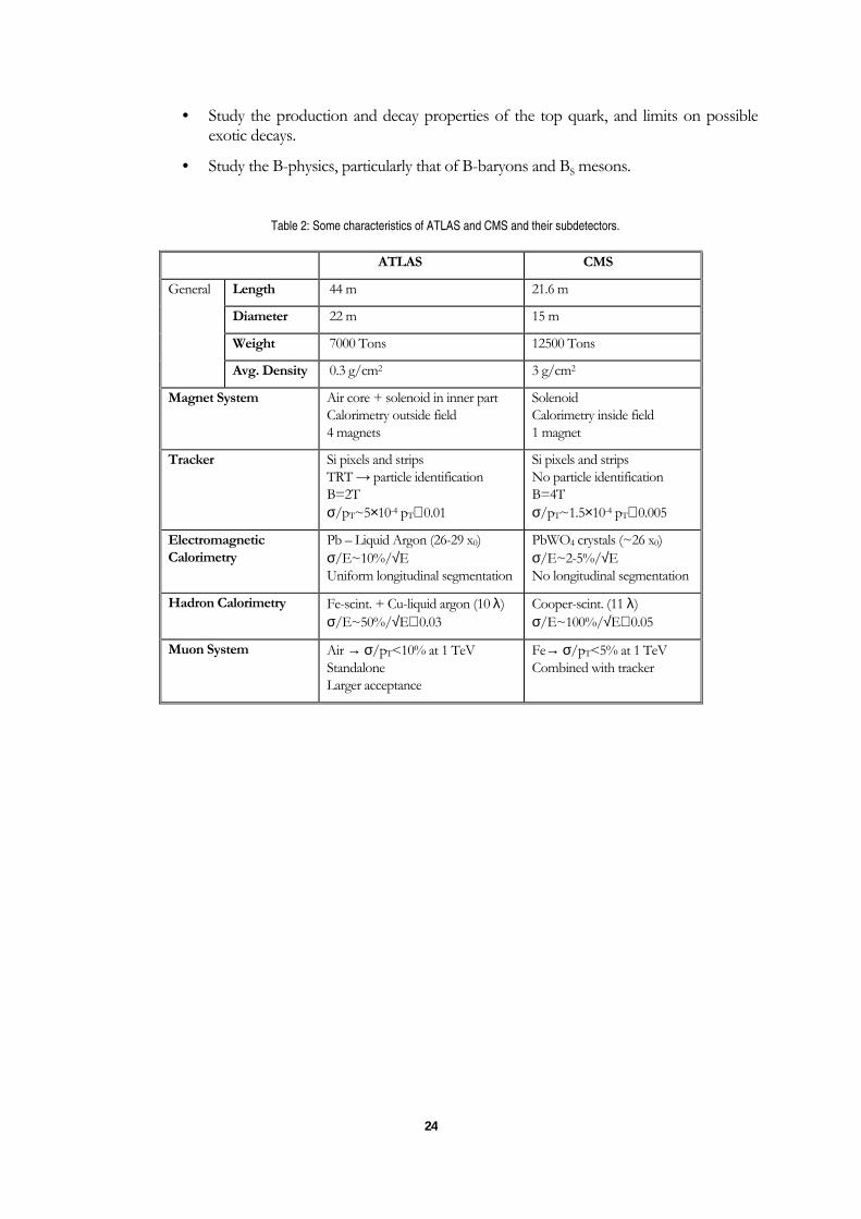
In Table 2 some of the characteristics of the two general purpose experiments for the LHC (ATLAS and CMS) are summarized. These experiments are presented in detail in the following subsections.
The fundamental physics goal of both ATLAS and CMS is exploring the physics behind electroweak symmetry breaking, and more specifically:
• Discover or exclude the standard Model Higgs and/or the multiple Higgs bosons of supersymmetric theories.
• Discover or exclude supersymmetry over the entire theoretically allowed mass range.
• Discover or exclude new dynamics at the electroweak scale.
• Discover or exclude any new electroweak gauge bosons with masses below several TeV.
• Discover or exclude any new quarks or leptons that are kinematically accessible.
24
• Study the production and decay properties of the top quark, and limits on possible exotic decays.
• Study the B-physics, particularly that of B-baryons and BS mesons.
Table 2: Some characteristics of ATLAS and CMS and their subdetectors.
ATLAS CMS
Length 44 m 21.6 m
Diameter 22 m 15 m
Weight 7000 Tons 12500 Tons
General
Avg. Density 0.3 g/cm2 3 g/cm2
Magnet System Air core + solenoid in inner part Calorimetry outside field 4 magnets
Solenoid Calorimetry inside field 1 magnet
Tracker Si pixels and strips TRT → particle identification B=2T σ/pT~5×10-4 pT⊕0.01
Si pixels and strips No particle identification B=4T σ/pT~1.5×10-4 pT⊕0.005
Electromagnetic
Calorimetry
Pb – Liquid Argon (26-29 x0) σ/E~10%/√E Uniform longitudinal segmentation
PbWO4 crystals (~26 x0) σ/E~2-5%/√E No longitudinal segmentation
Hadron Calorimetry Fe-scint. + Cu-liquid argon (10 λ) σ/E~50%/√E⊕0.03
Cooper-scint. (11 λ) σ/E~100%/√E⊕0.05
Muon System Air → σ/pT<10% at 1 TeV Standalone Larger acceptance
Fe→ σ/pT<5% at 1 TeV Combined with tracker

25
3.2 Compact Muon Solenoid (CMS) The Compact Muon Solenoid (CMS) experiment (shown in Figure 7 and Figure 8) has been
designed to detect cleanly the diverse signatures of new physics at the LHC. It will do so by identifying and precisely measuring the tracks of muons, electrons and photons over a large energy range, by determining the signatures of quarks and gluons through the measurement of charged and neutral particles (hadrons) with moderate precision and by measuring missing transverse energy flow (which is the signature of neutrinos and non-interacting new particles).
Figure 7: Three-dimensional view of the subdetectors in CMS. Note the endcaps shown in the lower left corner.
3.2.1 Inner Detector
The tracking system is expected to play an essential role for an experiment addressed to the full range of physics that will be accessed in the LHC. Experience has shown that robust tracking and vertex reconstruction within a strong magnetic field are powerful tools to identify and measure muons, electrons, photons and jets over a large energy range.
An all-silicon solution has been chosen for the tracking detector of CMS, implementing 25000 silicon strip sensors covering an area of 210 m2. They are connected to 75000 Analog Pipeline Voltage (APV) mode chips, having control on 9600000 read-out channels.

26
Figure 8: Axial view of CMS. The different subdetectors and the track of a muon in the magnetic field are displayed.
At the smallest radii from the beam line the interaction region is surrounded by two layers of Silicon Pixel detectors. The coverage is completed with two endcap disks, as shown in Figure 9.
Figure 9: Drawing of the Silicon Pixel detector, where the two layers in the central region and the endcap disks can
be seen.
The layout for the silicon strip detector, as Figure 10 shows, has four Tracker Inner Barrel (TIB) layers (the two first layers are double sided) complemented by two Tracker Inner Disks (TID), each composed of three small discs. The Tracker Outer Barrel (TOB), where the modules are assembled in six concentric layers (the first two also double sided) closes the tracker toward the calorimeters. Two Tracker EndCaps (TEC) ensure a pseudorapidity coverage of |η|<2.5. The endcap modules are mounted on 18 discs (each with 7 rings and covering 1/16 of the whole 2π angle). The Part 1 of this report is dedicated to the study of the TOB modules performance in system tests.

27
Figure 10: On the left, axial view of the different parts of the Tracker system in the barrel region. On the right, three-dimensional
layout of the CMS tracking detectors, where the different parts mentioned in the text can be observed.
3.2.2 Electromagnetic Calorimetry: ECAL and Preshower
The Electromagnetic Calorimeter (ECAL) will play an essential role in the study of the physics of electroweak symmetry breaking, particularly through the exploration of the Higgs sector. The search for the Higgs at the LHC will strongly rely on information from the ECAL by measuring the two-photon decay mode for mH ≤150 GeV and by measuring the electrons and positrons from the decay of Ws and Zs originating from the H→ZZ(*) and H→WW decay chain for 140 GeV≤ mH ≤ 700 GeV.
A scintillating crystal calorimeter has been chosen for the ECAL, which offers the best performance for energy resolution since most of the energy from electrons or photons is deposited within the homogeneous crystal volume of the calorimeter.
Figure 11: On the left, picture of one of the crystals to be used in the ECAL barrel with its photodiodes. On the right, three-
dimensional view of the electromagnetic calorimeter.
The calorimeter will consist of over 80000 lead tungstate (PbWO4) crystals which have a fast response, as well as high density, a small Molière radius and a short radiation length. A picture of the crystals and a schematic view of the ECAL can be seen in Figure 11. All this allow a very compact calorimeter system.

28
The crystals used in the barrel have a front face of about 22×22 mm2. To limit the fluctuations on the longitudinal shower leakage of high-energy electrons and photons, the crystals have a total thickness of 26 radiation lengths (about only 23 cm). In the endcaps, the crystals are slightly wider (30×30 mm2) and shorter (22 cm long). The light produced in the crystals is read-out by photodectors (avalanche photodiodes), resulting a electric pulse which is then amplified and digitized.
CMS will also use a preshower detector in the endcap region (1.65<|η|<2.6). Its main function is to provide γ-π0 separation in the forward region. At this rapidity, the energy of the neutral pions results in two closely-spaced decay photons indistinguishable from a single-photon shower decay in the ECAL.
The preshower detector (shown schematically in Figure 12) contains two thin lead converters followed by silicon strip detector planes placed in front of the ECAL, and measures the first part of the shower profile in two orthogonal silicon planes. It allows the determination of the impact position of the electromagnetic shower by a charge-weighted-average algorithm with the very good accuracy (∼300 µm at 50 GeV), enabling the separation of single showers from overlaps of two close showers as the ones mentioned before.
Figure 12: Schematic view of an event in the preshower detector.
3.2.3 Hadronic Calorimetry: HCAL
The Hadronic Calorimeter (HCAL) plays an essential role in the identification and measurement of quarks, gluons and also neutrinos (by measuring the energy and direction of jets and the missing transverse energy flow). Missing energy forms a crucial signature of new particles, like the supersymmetric partners of quarks and gluons. For having a good resolution in measuring this missing energy, a hermetic calorimetry coverage up to |η|≤5 is required. A schematic view of the calorimeter system is shown in Figure 13.
The Hadron Barrel (HB) and Hadron Endcap (HE) calorimeters are sampling calorimeters with 50 mm thick copper absorber plates interleaved with 4 mm thick scintillator sheets. Additional scintillating layers (Hadron Outer Barrel, HOB) are placed just outside the magnet coil for ensuring total shower energy containment. The full depth of the combined HB and HOB detectors is approximately 11 absorption lengths.
Two Hadronic Forward (HF) calorimeters completes the |η|<5 coverage, which use quartz fibers as the active medium, embedded in a steel absorber matrix. Because of the quartz fiberis predominant sensitive to Čerenkov light from neutral pions, it has the unique and desireable feature of a very localized response to hadronic showers.

29
Figure 13: Schematic view of one quadrant of the electromagnetic and hadronic calorimetry and the tracking system inside the
solenoid coil, where the different parts of the detectors can be seen.
3.2.4 Muon System
Muons are an unmistakable signature of most of the physics the LHC is designed to explore. The ability to trigger on and reconstruct muons at the highest luminosities is central to the concept of CMS.
CMS will use three types of gaseous particle detectors for muon identification: Drift Tubes (DT) in the central barrel region (0<|η|<1.3), Cathode Strip Chambers (CSC) in the endcap region (0.9<|η|<2.4), which provides high precision in the presence of a large and varying magnetic field and Resistive Parallel Plate Chambers (RPC) in both the barrel and the endcaps. The DT and CSC detectors are used to obtain a precise measurement of the position (and thus the momentum) of the muons, whereas the RPC chambers are dedicated to providing fast information for the Level-1 trigger. A sophisticated alignment system relates the positions of the muon detectors to those of the central tracker elements to provide maximum momentum resolution.
The disposition of all these detectors is shown in Figure 14.
Figure 14: Schematic view of the different muon detectors and their emplacement in CMS.

30
3.2.5 Magnet System
CMS will use a large superconducting solenoid with a length of around 12 m and an inner diameter of about 6m. The field strength will be 4 Tesla. Due to the dimensions of the coil, the tracker and the calorimeters will be placed inside the magnet, resulting in a compact overall detector.
Outside the coil a steel return yoke will be placed in the barrel and endcap regions with a diameter of 14 meters and a length of 21.6 m. This yoke is built in layers, interspersed with muon detectors. With this configuration of the magnetic field, the momentum of the muons will be measured both inside the coil (by tracking devices) and outside the coil (by the muon chambers).

31
3.3 A Toroidal LHC AparatuS (ATLAS) ATLAS (A Toroidal LHC ApparatuS) is a general-purpose p-p spectrometer designed to
exploit the full discovery potential of the LHC. Figure 15 shows an illustration of ATLAS. The detector design is optimized for a long range of known, expected and hypothetical process. This includes a very good electromagnetic calorimetry (for electron and photon identification and measurements), complemented by full-coverage hadronic calorimetry (for accurate jet and missing transverse energy measurements), a high-precision muon measurements and a very efficient tracking system. In the following sections, the different ATLAS subdetectors are presented and discussed.
Figure 15: Three-dimensional view of the ATLAS detector.
3.3.1 Inner Detector
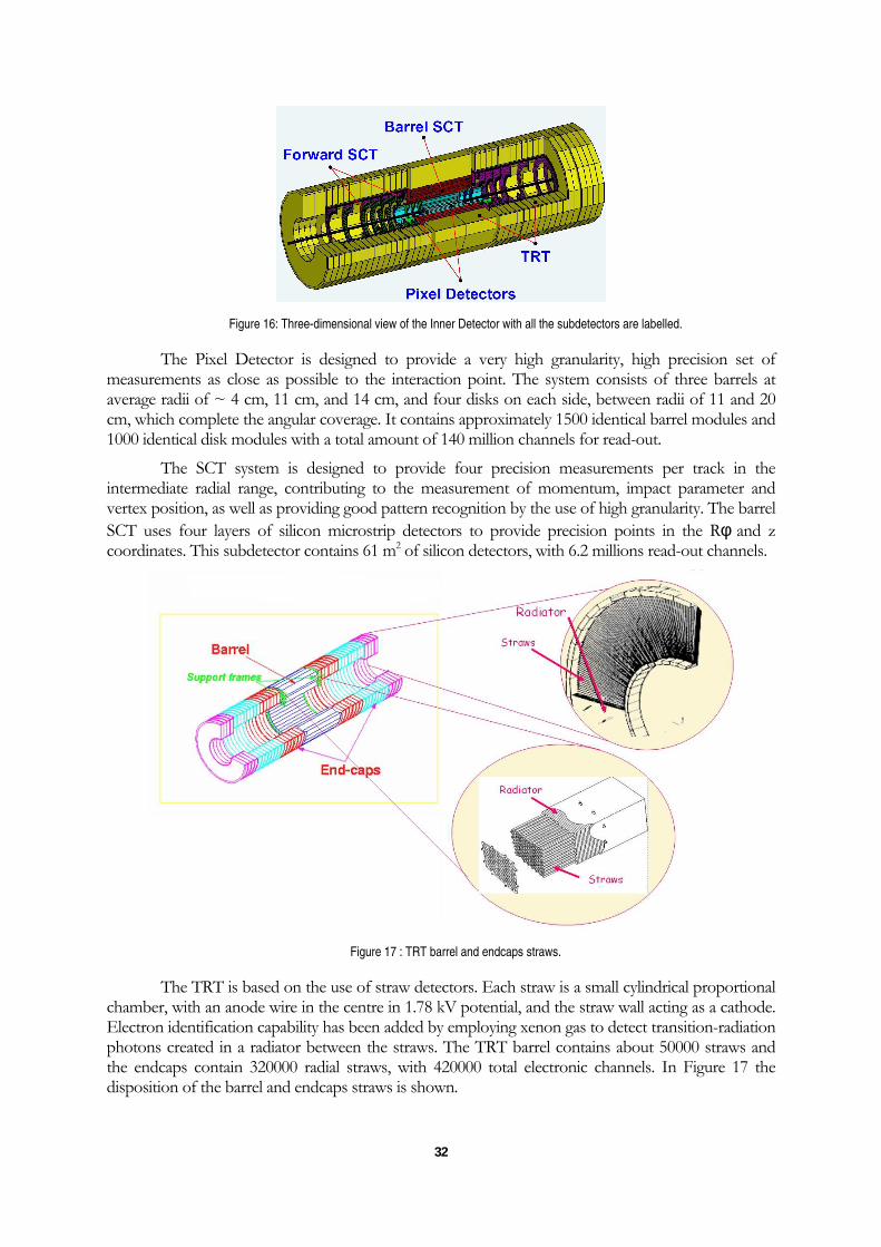
The task of the Inner Detector (ID) is to reconstruct the tracks and vertices in the events with high efficiency, contributing together with the calorimeter and muon systems to the electron, photon and muon recognition, and supplying important extra signatures for short-lived particle decay vertices. In ATLAS, the ID covers the pseudo-rapidity range |η|<2.5. A three-dimensional view of the Inner detector is shown in Figure 16.
Silicon microstrip and pixel detectors are used for achieving a high-precision measurement in the part closest to the interaction point. Around the vertex region, Pixel Detectors are used, providing a very high granularity. In the outer layer, the SemiConductor Tracker (SCT) which uses silicon microstrip detectors is placed. To increase the number of tracking points, the Transition Radiation Tracker (TRT) is used, based on straw detectors, which provides the possibility of continuous track and electron identification. The combination of the two techniques (silicon and straw detectors) gives very robust pattern recognition and high precision in both φ and z coordinates, with an average of six precision space-points measurements and 36 straws per track.
32
Figure 16: Three-dimensional view of the Inner Detector with all the subdetectors are labelled.
The Pixel Detector is designed to provide a very high granularity, high precision set of measurements as close as possible to the interaction point. The system consists of three barrels at average radii of ~ 4 cm, 11 cm, and 14 cm, and four disks on each side, between radii of 11 and 20 cm, which complete the angular coverage. It contains approximately 1500 identical barrel modules and 1000 identical disk modules with a total amount of 140 million channels for read-out.
The SCT system is designed to provide four precision measurements per track in the intermediate radial range, contributing to the measurement of momentum, impact parameter and vertex position, as well as providing good pattern recognition by the use of high granularity. The barrel SCT uses four layers of silicon microstrip detectors to provide precision points in the Rφ and z coordinates. This subdetector contains 61 m2 of silicon detectors, with 6.2 millions read-out channels.
Figure 17 : TRT barrel and endcaps straws.
The TRT is based on the use of straw detectors. Each straw is a small cylindrical proportional chamber, with an anode wire in the centre in 1.78 kV potential, and the straw wall acting as a cathode. Electron identification capability has been added by employing xenon gas to detect transition-radiation photons created in a radiator between the straws. The TRT barrel contains about 50000 straws and the endcaps contain 320000 radial straws, with 420000 total electronic channels. In Figure 17 the disposition of the barrel and endcaps straws is shown.
33
3.3.2 Calorimetry
At the LHC about twenty soft collisions per bunch crossing will be produced. In consequence fast detector response and fine granularity are required to minimise the impact of the pile-up on the physics performance.
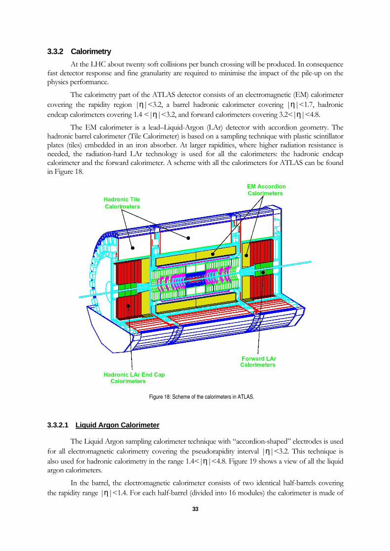
The calorimetry part of the ATLAS detector consists of an electromagnetic (EM) calorimeter covering the rapidity region |η|<3.2, a barrel hadronic calorimeter covering |η|<1.7, hadronic endcap calorimeters covering 1.4 <|η|<3.2, and forward calorimeters covering 3.2<|η|<4.8.
The EM calorimeter is a lead–Liquid-Argon (LAr) detector with accordion geometry. The hadronic barrel calorimeter (Tile Calorimeter) is based on a sampling technique with plastic scintillator plates (tiles) embedded in an iron absorber. At larger rapidities, where higher radiation resistance is needed, the radiation-hard LAr technology is used for all the calorimeters: the hadronic endcap calorimeter and the forward calorimeter. A scheme with all the calorimeters for ATLAS can be found in Figure 18.
Figure 18: Scheme of the calorimeters in ATLAS.
3.3.2.1 Liquid Argon Calorimeter
The Liquid Argon sampling calorimeter technique with “accordion-shaped” electrodes is used for all electromagnetic calorimetry covering the pseudorapidity interval |η|<3.2. This technique is also used for hadronic calorimetry in the range 1.4<|η|<4.8. Figure 19 shows a view of all the liquid argon calorimeters.
In the barrel, the electromagnetic calorimeter consists of two identical half-barrels covering the rapidity range |η|<1.4. For each half-barrel (divided into 16 modules) the calorimeter is made of

34
1024 accordion-shaped absorbers alternating with 1024 read-out electrodes, arranged with a complete φ symmetry around the beam axis. Between each pair of absorbers, there are two liquid argon gaps, separated by a read-out electrode.
Inside the encap cryostat (see Section 3.3.4) is placed the electromagnetic EndCap calorimeter (EMEC), the Hadronic EndCap calorimeter (HEC) and the Forward Calorimeter (FCAL). The EMEC, which covers the range 1.375<|η|<3.2, uses the same technique as in the barrel part.
Figure 19: Three-dimensional view of the LAr calorimeters.
The HEC covers the range 1.5<|η|<3.2 and uses copper-plates as absorbers, with parallel geometry in this case. The FCAL covers the range 3.2<|η|<4.9 providing coverage for electromagnetic and hadronic showers by using copper and tungsten as absorbers, respectively.
The EM calorimeter is segmented in three longitudinal samplings in the |η|<2.5 region and in two samples in the |η|>2.5 region. The total thickness of the EM calorimeter is above 24 radiation lengths for the barrel and above 26 for the endcaps.
3.3.2.2 Tile Calorimeter (TileCal)
The Tile Calorimeter is a sampling device made out of steel and scintillating tiles as absorber and active material respectively. It is divided in three sections: the Central Barrel (CB) and two Extended Barrels (EBs). The barrel covers the region |η|<1.0, and the extended barrels cover the region 0.8<|η|<1.7. Azimuthally, the Barrel and Extended Barrels are divided into 64 modules, as shown in Figure 20. The full depth of the TileCal is above 7 absorption lengths in the CB and about 10 in the EB.
The tiles are placed perpendicular to the colliding beams. This consist the main innovation of TileCal because in most hadonic calorimeters the active elements are placed longitudinally. This design optimizes the homogeneity in the signal sampling in the active elements. The structure is periodic along z. The tiles are 3 mm thick and the total thickness of the iron plates in one period is 14 mm.
The light produced in the scintillating tiles has wavelength in the ultraviolet region and intensity proportional to the energy deposited by the particles. Both sides of the scintillating tiles are read-out along the outside faces of each module by WaveLength Shifting (WLS) fibers into two separate PhotoMultiplier Tubes (PMTs) to achieve a redundant read-out. The WLS fibers shift the light to longer wavelengths, in order to match the sensitive region of the PMT. Figure 21 shows the disposition of the tiles, the fibers and the PMTs in a module.

35
Figure 20: Three-dimensional view of the TileCalorimeter.
Figure 21: Principle of the TileCal design.
The use of fiber read-out allows defining a three-dimensional cell read-out, creating a projective geometry to the interaction region for triggering and energy reconstruction, as Figure 22 shows. TileCal has a three samplings longitudinal segmentation, with a ∆η×∆φ granularity equal to 0.1×0.1 in the first two samplings and 0.1×0.2 in the last sampling. A compact electronics read-out (called drawer) is housed in the girder of each module, and will be discussed detaily in Section 11.1.
The Part 2 of this report is dedicated to software developments for the TileCal back-end electronics.
Figure 22: Layout of the cells of the Tilecal Barrel (left) and Extended Barrel (right) modules.
3.3.3 Muon System
The ATLAS Collaboration has designed a high-resolution muon spectrometer with stand-alone triggering and momentum measurement capability over a wide range of transverse momentum, pseudorapidity and azimuthal angle. Four chamber technologies are employed in the detector. The positions of these stations are optimized for good hermeticity and optimum momentum resolution. A three-dimensional view of the muon spectrometer system is shown in Figure 23 and a two-dimensional view in the xy direction is shown in Figure 24.
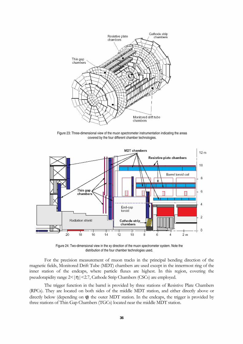
36
Figure 23: Three-dimensional view of the muon spectrometer instrumentation indicating the areas
covered by the four different chamber technologies.
Figure 24: Two-dimensional view in the xy direction of the muon spectrometer system. Note the
distribution of the four chamber technologies used.
For the precision measurement of muon tracks in the principal bending direction of the magnetic fields, Monitored Drift Tube (MDT) chambers are used except in the innermost ring of the inner station of the endcaps, where particle fluxes are highest. In this region, covering the pseudorapidity range 2<|η|<2.7, Cathode Strip Chambers (CSCs) are employed.
The trigger function in the barrel is provided by three stations of Resistive Plate Chambers (RPCs). They are located on both sides of the middle MDT station, and either directly above or directly below (depending on φ) the outer MDT station. In the endcaps, the trigger is provided by three stations of Thin Gap Chambers (TGCs) located near the middle MDT station.

37
3.3.4 Magnet System
An optimised magnetic field configuration for particle bending around the various detectors in a light and open structure which minimizes scattering effects has been chosen in ATLAS. The final arrangement consists of a central solenoid servicing the inner detector trackers with an axial magnetic field, surrounded by a system of three large scale air-core toroids generating a tangential magnetic field for the muon spectrometer, as can be seen schematically in Figure 25. The niobium-Titanium (NbTi) superconductor in a copper (Cu) matrix technology is used in this case. The magnet system weights 1300 tons and is cooled by liquid helium at 4.5 K (which needs 40 days to reach this temperature).
Figure 25 : ATLAS magnet system scheme (on the left) and simulation (on the right). Note the
central solenoid and the three toroids.
Hence, the subsystems are the Central Solenoid (CS), Barrel Toroid (BT) and two EndCap Toroids (ECT). The CS is a superconducting solenoid made as a single layer coil. It is magnetically decoupled from the toroid magnets and is mounted in the same cryostat as the LAr Calorimeter. This solenoid provides a 2 Tesla strong field along in the interaction point which drops to 0.5 T at the end of the ID.
The BT covers the central region and provides a 2 - 6 Tm magnetic field integral. It is build up from eight flat racetrack magnets each of them consisting of two double pancake windings housed in a common aluminium casing. The two ECTs toroids are positioned inside the Barrel Toroid at each end of the Central Solenoid, providing a 4-8 Tm magnetic field integral. In contrast to the Barrel Toroid, the eight coils of each End Cap Toroid are assembled inside a single cryostat. A simulation of these subsystems can also be seen in Figure 25.

38
39
Part 1: Performance of CMSPerformance of CMSPerformance of CMSPerformance of CMS TOB Silicon TOB Silicon TOB Silicon TOB Silicon
Detector Modules on a Double Detector Modules on a Double Detector Modules on a Double Detector Modules on a Double
Sided Prototype Sided Prototype Sided Prototype Sided Prototype RodRodRodRod

40
4 Introduction As mentioned before, the CMS inner tracking strategy relies on the SST (Silicon Strip Tracker)
detector. The six outermost central layers of the SST form the Tracker Outer Barrel (TOB) detector. Figure 26 shows a two-dimensional sketch of a quadrant of the CMS tracker. In the case of the TOB, the two innermost layers are double sided (in dark blue in Figure 26) and the rest are single sided (in grey in Figure 26).
Figure 26: Sketch of the CMS tracker layout (a quarter of the z view, without the pixel detector). Grey lines
represent single modules and blue lines double modules. See also Figure 10.
The TOB silicon modules, the services and cables, and the electronics needed for the functioning of the detectors are installed into independent supporting read-out elements called rods, which will be placed inside a supporting wheel in the final design for CMS. Each TOB layer is made of two rods in z, each rod containing 6 or 12 detectors.
4.1 Silicon Detector Modules Description The TOB is made of 3048 single silicon detector modules and 1080 double modules (5208
detectors in total). Each detector module is made out of two sensors with a 1mm gap between them. Each sensor is made of one 6-inch wafer, with an active area of 94×186 mm2. The r-φ detectors have a 4 or 6 APVs, for a pitch of 183 or 122 microns. The stereo detectors (tilted about 6 degrees from the axis system) have 4 APVs for a pitch of 183 microns. See Table 3 for more details.
4.2 Read-out Electronics The detector modules are equipped with front-end hybrids housing Application-Specific
Integrated Circuit (ASIC) APV25 chips for analogue read-out. The chip contains 128 channels of preamplifier and shaper driving 192 columns of analogue storage into which samples are written at the 40 MHz frequency of the LHC bunch crossing. Therefore, the memory always contains a record of the hits resulting from the most recent bunch crossing that the chip has sensed. A data access mechanism allows the marking and queuing of requested memory locations for output. The analog outputs from two APV chips are multiplexed on a single line to the Analog OptoHybrids (AOHs), where the signal is converted from electrical to optical. The data is then transmitted to the control
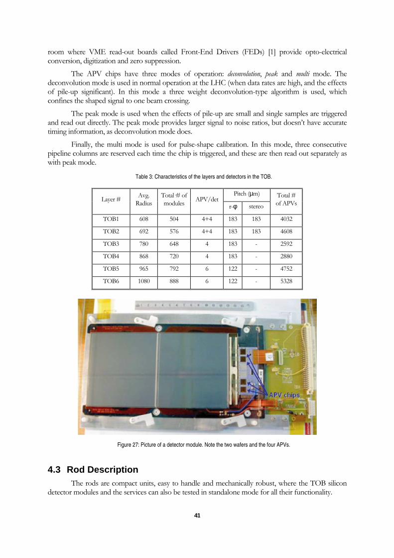
41
room where VME read-out boards called Front-End Drivers (FEDs) [1] provide opto-electrical conversion, digitization and zero suppression.
The APV chips have three modes of operation: deconvolution, peak and multi mode. The deconvolution mode is used in normal operation at the LHC (when data rates are high, and the effects of pile-up significant). In this mode a three weight deconvolution-type algorithm is used, which confines the shaped signal to one beam crossing.
The peak mode is used when the effects of pile-up are small and single samples are triggered and read out directly. The peak mode provides larger signal to noise ratios, but doesn’t have accurate timing information, as deconvolution mode does.
Finally, the multi mode is used for pulse-shape calibration. In this mode, three consecutive pipeline columns are reserved each time the chip is triggered, and these are then read out separately as with peak mode.
Table 3: Characteristics of the layers and detectors in the TOB.
Pitch (µm) Layer #
Avg. Radius
Total·# of modules
APV/det r-φ stereo
Total # of APVs
TOB1 608 504 4+4 183 183 4032
TOB2 692 576 4+4 183 183 4608
TOB3 780 648 4 183 - 2592
TOB4 868 720 4 183 - 2880
TOB5 965 792 6 122 - 4752
TOB6 1080 888 6 122 - 5328
Figure 27: Picture of a detector module. Note the two wafers and the four APVs.
4.3 Rod Description The rods are compact units, easy to handle and mechanically robust, where the TOB silicon
detector modules and the services can also be tested in standalone mode for all their functionality.
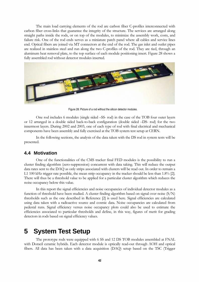
42
The main load carrying elements of the rod are carbon fiber C-profiles interconnected with carbon fiber cross-links that guarantee the integrity of the structure. The services are arranged along straight paths inside the rods, or on top of the modules, to minimize the assembly work, costs, and failure risk. One of the rod ends serves as a miniature patch panel where all cables and service lines end. Optical fibers are joined via MT connectors at the end of the rod. The gas inlet and outlet pipes are realized in stainless steel and run along the two C-profiles of the rod. They are tied, through an aluminum heat removal plate, to the top surface of each module positioning insert. Figure 28 shows a fully assembled rod without detector modules inserted.
Figure 28: Picture of a rod without the silicon detector modules.
One rod includes 6 modules (single sided –SS- rod) in the case of the TOB four outer layers or 12 arranged in a double sided back-to-back configuration (double sided –DS- rod) for the two innermost layers. During 2002 and 2003, one of each type of rod with final electrical and mechanical components have been assembly and fully exercised at the TOB system test setup at CERN.
In the following sections, the analysis of the data taken with the DS rod in system tests will be presented.
4.4 Motivation One of the functionalities of the CMS tracker final FED modules is the possibility to run a
cluster finding algorithm (zero-suppression) concurrent with data taking. This will reduce the output data rates sent to the DAQ as only strips associated with clusters will be read out. In order to remain a L1 100 kHz trigger rate possible, the mean strip occupancy in the tracker should be less than 1.8% [2]. There will thus be a threshold value to be applied for a particular cluster algorithm which reduces the noise occupancy below this value.
In this report the signal efficiencies and noise occupancies of individual detector modules as a function of threshold have been studied. A cluster finding algorithm based on signal over noise (S/N) thresholds such as the one described in Reference [2] is used here. Signal efficiencies are calculated using data taken with a radioactive source and cosmic data. Noise occupancies are calculated from pedestal runs. Signal efficiency versus noise occupancy plots could also be used to estimate the efficiencies associated to particular thresholds and define, in this way, figures of merit for grading detectors in rods based on signal efficiency values.
5 System Test Setup The prototype rods were equipped with 6 SS and 12 DS TOB modules assembled at FNAL
with Doracil ceramic hybrids. Each detector module is optically read-out through AOH and optical fibers. All data has been taken with a data acquisition (DAQ) setup based on the TSC (Trigger

43
Sequencer Card), a PCI Mezzanine Card - Front-End Control (PMC-FEC) card with electrical controls and three PMC-FED cards using the XROD DAQ program [3].
Special pedestal runs with internal triggers at fixed rates and a random trigger pipeline were taken for the noise studies. Signal to noise measurements and signal efficiencies were also performed from a Ru106 radioactive source and cosmic ray data runs taken with scintillators connected to NIM logic electronics. The scintillator signal is forced to come within a time window in the corresponding 25 ns integration cycle. During data taking, all modules in the rod were kept at a full depletion bias voltage of 200 Volts. All results shown in the next sections correspond to both peak and deconvolution APV operation settings.
6 Noise Analysis
6.1 Definitions The physical magnitudes used in the study of the noise performance of silicon strip detectors
used in this report are described below:
• Pedestals: the pedestal for a given channel i, pedi, is defined as the mean digitized charge (νi) in absence of a known signal:
iiped ν=
• Noise: assuming a Gaussian distribution of pedestals, the noise of channel i, σi, is defined as the standard deviation of the pedestal distribution:
( ) 222
iiiii ped νννσ −=−=
This noise is usually referred to as raw noise.
• Common Mode Noise (CMN): the CMN refers to a variation of the signal which affects groups of channels in a coherent way. It can be caused by a common electromagnetic pick-up, noise on the voltage power supply, etc. The susceptibility to common mode noise depends on the individual detector modules and on the system environment. The CMN is usually obtained for a given chip by calculating the fluctuations of the average pedestal of all channels in a chip on an event by event basis, and it’s usually calculated as the average of the difference between the output voltage and the mean pedestal over channels:
channelsii pedCMN −= ν
• Differential Noise: the differential noise for a given channel i, σi d, is defined as 1/√2 of
the standard deviation between the output voltage νi for that channel and the output voltage νi+1 of a neighbor channel:
( ) ( )2
2
1
2
1 ++ −−−=
iiiid
i
ννννσ
The differential noise is useful as it represents an irreducible detector noise not due to pickup, poor grounding, etc. It can be also written as:

44
( ) 1
2
1
2
11
2
1
22
22+
+++
+ −+
=+−+
= ii
ii
iiii
iid
i σρσσσννννσσσ
where ρ is the correlation between νi and νi+1. Assuming σi=σi+1, i.e., that the consider channel and its neighbour have the same noise, we have:
( ) ( )ρσσ −= 122
i
d
i
The differential noise is thus equal to the noise if there is no correlation between the output voltage of the channels, and it is less than the noise if there is a positive correlation between the output voltage of the channel. A positive correlation can be due to a common component of the noise induced by external pickup.
• Common mode subtracted noise (CMS-like noise): taking into account the CMN, one can define the common mode noise subtracted charge (in absence of signal) for a given channel i as:
CMNpedii
CMS
i −−=νν
The common mode subtracted noise is defined as the standard deviation of the above distribution:
22 CMS
i
CMS
i
CMS
i ννσ −=
6.2 Results The results of the analysis of the data taken in pedestal runs are presented in the following
sections. In general, the pedestal and noise figures on the detectors do not vary much along the position of the modules in the rod. From now on only results from two particular detector modules out of the 12 which the rod is equipped with (referred to as modules 4 and 5) will be shown. These detectors lie back to back on the end of the rod opposite to the Connection and Control Unit (CCU) module control card and will be used later (Section 7) to study signal efficiencies and signal to noise ratios from beta source and cosmic ray runs. All results shown correspond to both peak and deconvolution APV operation modes.
6.2.1 Pedestals
The mean pedestal values for each of the 512 strips in modules 4 and 5 are shown in Figure 29 as a function of channel number. Results are shown for both peak and deconvolution modes. In most of the cases it can be seen large differences in the analog data baselines of the different APV chips.
6.2.2 Noise
Figure 30 and Figure 31 show the values of the total raw noise, the differential noise and the CMS-like noise (as defined in Section 6.1) as a function of strip number. The results are shown for both deconvolution and peak modes, respectively.
The noise distributions are very stable as a function of channel number and no significant edge strip noise effects as seen in the UTRI setup1 are observed with the rod setup. Channels with an abnormally low noise value are usually associated to dead channels (no response from calibration pulses). Channels with an abnormally high noise are usually associated to missing or open bondings
1 This is a test system for single modules based on the Ultima Tracker Read-out Interface (UTRI) board, where full electrical read-out was used.
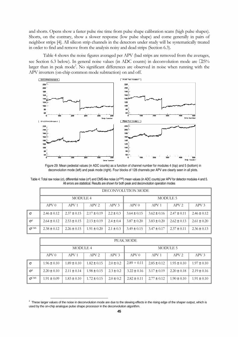
45
and shorts. Opens show a faster pulse rise time from pulse shape calibration scans (high pulse shapes). Shorts, on the contrary, show a slower response (low pulse shape) and come generally in pairs of neighbor strips [4]. All silicon strip channels in the detectors under study will be systematically treated in order to find and remove from the analysis noisy and dead strips (Section 6.3).
Table 4 shows the noise figures averaged per APV (bad strips are removed from the averages, see Section 6.3 below). In general noise values (in ADC counts) in deconvolution mode are ∼25% larger than in peak mode2. No significant differences are observed in noise when running with the APV inverters (on-chip common mode subtraction) on and off.
Figure 29: Mean pedestal values (in ADC counts) as a function of channel number for modules 4 (top) and 5 (bottom) in
deconvolution mode (left) and peak mode (right). Four blocks of 128 channels per APV are clearly seen in all plots.
Table 4: Total raw noise (σ), differential noise (σd) and CMS-like noise (σCMS) mean values (in ADC counts) per APV for detector modules 4 and 5. All errors are statistical. Results are shown for both peak and deconvolution operation modes
DECONVOLUTION MODE
MODULE 4 MODULE 5
APV 0 APV 1 APV 2 APV 3 APV 0 APV 1 APV 2 APV 3
σ 2.46 ± 0.12 2.37 ± 0.15 2.17 ± 0.19 2.2 ± 0.3 3.64 ± 0.15 3.62 ± 0.16 2.47 ± 0.11 2.46 ± 0.12
σd 2.64 ± 0.12 2.53 ± 0.15 2.13 ± 0.19 2.4 ± 0.4 3.87 ± 0.20 3.83 ± 0.20 2.62 ± 0.13 2.61 ± 0.20
σCMS 2.38 ± 0.12 2.26 ± 0.15 1.91 ± 0.20 2.1 ± 0.3 3.49 ± 0.15 3.47 ± 0.17 2.37 ± 0.11 2.36 ± 0.13
PEAK MODE
MODULE 4 MODULE 5
APV 0 APV 1 APV 2 APV 3 APV 0 APV 1 APV 2 APV 3
σ 1.96 ± 0.10 1.89 ± 0.10 1.82 ± 0.15 2.0 ± 0.2 2.89 + 0.11 2.85 ± 0.12 1.95 ± 0.10 1.97 ± 0.10
σd 2.20 ± 0.10 2.11 ± 0.14 1.98 ± 0.15 2.3 ± 0.2 3.22 ± 0.16 3.17 ± 0.19 2.20 ± 0.18 2.19 ± 0.16
σCMS 1.91 ± 0.09 1.83 ± 0.10 1.72 ± 0.15 2.0 ± 0.2 2.82 ± 0.11 2.77 ± 0.12 1.90 ± 0.10 1.91 ± 0.10
2 These larger values of the noise in deconvolution mode are due to the slewing effects in the rising edge of the shaper output, which is used by the on-chip analogue pulse shape processor in the deconvolution algorithm.
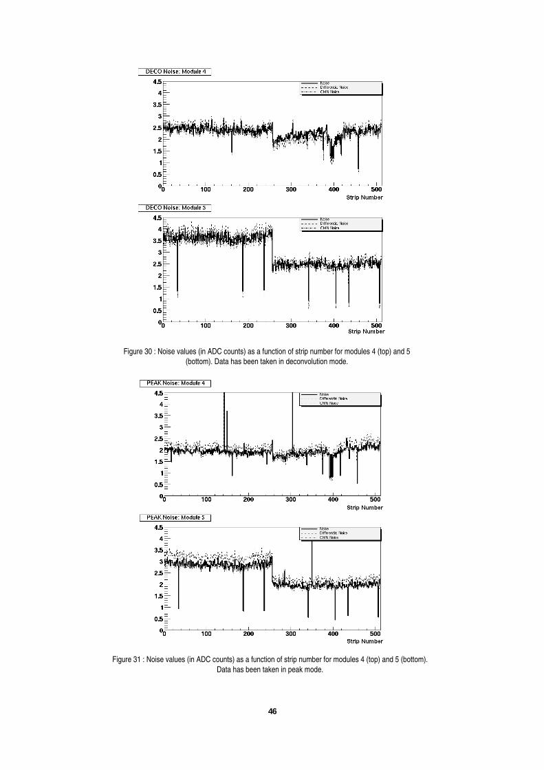
46
Figure 30 : Noise values (in ADC counts) as a function of strip number for modules 4 (top) and 5
(bottom). Data has been taken in deconvolution mode.
Figure 31 : Noise values (in ADC counts) as a function of strip number for modules 4 (top) and 5 (bottom).
Data has been taken in peak mode.

47
Although the total noise and the common mode noise subtracted noise are similar (no significant contribution of common mode noise is seen), the differential noise shows slighter values above the total noise. This indicates a small noise anticorrelation between channels.
6.2.3 Common Mode Noise
Figure 30, Figure 31 and Table 4 show total raw noise values similar to final common mode subtracted noise. This indicates an absence of significant common mode noise picked up by the modules in our setup and a good grounding of the silicon modules in the rod and DAQ electronics. Figure 32 shows the distribution of the common mode noise per APV for modules 4 and 5. Results are shown only for deconvolution mode, with and without the inverters switched on. The CMN with inverters off accounts to ~0.5 ADC counts. The CMN is reduced ∼30% when data is taken with inverters on. Table 5 summarizes these results.
Table 5: Mean values and sigma for the CMN distributions (in ADC counts) shown in Figure 32.
DECONVOLUTION MODE Inverters ON Inverters OFF <CMN> σCMN <CMN> σCMN
APV 0 0.183 0.142 0.276 0.370 APV 1 0.150 0.371 0.257 0.435 APV 2 0.041 0.856 0.039 0.656
Module 4
APV 3 0.015 0.200 0.401 0.290 APV 0 0.009 0.207 0.090 0.501 APV 1 -0.09 0.211 0.050 0.490 APV 2 0.108 0.210 0.150 0.385
Module 5
APV 3 0.123 0.156 0.153 0.321
Figure 32: CMN distributions per APV (in ADC counts) for modules 4 (top) and 5 (bottom). All data shown corresponds to
deconvolution mode with inverters on (solid histograms) and off (dashed histograms).
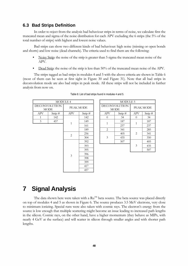
48
6.3 Bad Strips Definition In order to reject from the analysis bad behaviour strips in terms of noise, we calculate first the
truncated mean and sigma of the noise distribution for each APV excluding the 6 strips (the 5% of the total number of strips) with highest and lowest noise values.
Bad strips can show two different kinds of bad behaviour: high noise (missing or open bonds and shorts) and low noise (dead channels). The criteria used to find them are the following:
• Noisy Strip: the noise of the strip is greater than 5 sigma the truncated mean noise of the APV.
• Dead Strip: the noise of the strip is less than 50% of the truncated mean noise of the APV.
The strips tagged as bad strips in modules 4 and 5 with the above criteria are shown in Table 6 (most of them can be seen at first sight in Figure 30 and Figure 31). Note that all bad strips in deconvolution mode are also bad strips in peak mode. All these strips will not be included in further analysis from now on.
Table 6: List of bad strips found in modules 4 and 5.
MODULE 4 MODULE 5 DECONVOLUTION
MODE PEAK MODE DECONVOLUTION
MODE PEAK MODE
APV Strip # APV Strip # APV Strip # APV Strip # 1 142 142 0 34 0 34 3 457 149 187 187 161
1 237
1 237
1
189 2 341 285 256 405 341
2 304 435
2 350
392 3
507 405 393 435 395
3 507
396 398 399 417
3
457
7 Signal Analysis The data shown here were taken with a Ru106 beta source. The beta source was placed directly
on top of modules 4 and 5 as shown in Figure 6. The source produces 3.5 MeV electrons, very close to minimum ionizing. Special runs were also taken with cosmic rays. The electron’s energy from the source is low enough that multiple scattering might become an issue leading to increased path lengths in the silicon. Cosmic rays, on the other hand, have a higher momentum (they behave as MIPs, with nearly 4 GeV at the surface) and will scatter in silicon through smaller angles and with shorter path lengths.

49
Figure 33: Placement of the beta source relative to the position of the silicon modules in the
double-sided rod. All source and cosmic data shown correspond to this setup.
7.1 Cluster Algorithms and Cluster Thresholds The algorithm used for cluster finding is based in the following criteria:
• Cluster candidates are formed by selecting strips in a silicon detector module with a signal to noise ratio S/N>5 (seed strips).
• Adjacent strips to the seed strip are then added to the cluster only if their S/N>2.
Figure 34 shows the cluster multiplicity per event for modules 4 and 5 and for data taken with beta source and cosmic rays in deconvolution mode. Only non-empty events are shown. Figure 35 shows the strip multiplicity per cluster.
Figure 34: Cluster multiplicity per event for modules 4 (left) and 5 (right) from the beta source runs (top) and
cosmic ray data (bottom) always in deconvolution mode.
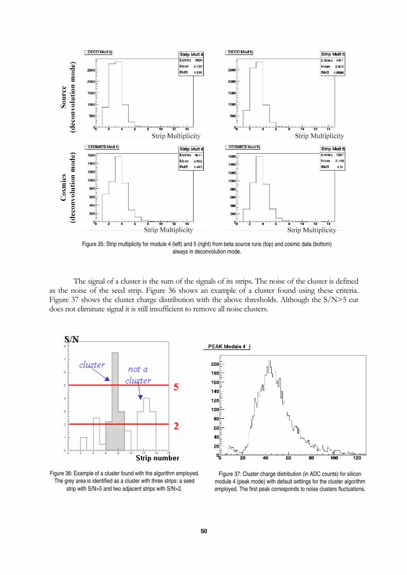
50
Figure 35: Strip multiplicity for module 4 (left) and 5 (right) from beta source runs (top) and cosmic data (bottom)
always in deconvolution mode.
The signal of a cluster is the sum of the signals of its strips. The noise of the cluster is defined as the noise of the seed strip. Figure 36 shows an example of a cluster found using these criteria. Figure 37 shows the cluster charge distribution with the above thresholds. Although the S/N>5 cut does not eliminate signal it is still insufficient to remove all noise clusters.
Figure 36: Example of a cluster found with the algorithm employed.
The grey area is identified as a cluster with three strips: a seed
strip with S/N>5 and two adjacent strips with S/N>2.
Figure 37: Cluster charge distribution (in ADC counts) for silicon
module 4 (peak mode) with default settings for the cluster algorithm
employed. The first peak corresponds to noise clusters fluctuations.

51
The thresholds to be used should minimize the number of clusters coming from noise fluctuations without sculpting the signal. By setting high thresholds one risks to remove clusters with low charge and bias the measured charged distribution yielding artificially high signal values. The final clustering threshold to be applied in the analysis is thus obtained by finding the lowest thresholds were noise clusters are not significant while not sculpting the signal.
7.2 Results The signal charge distributions have been fit using two different definitions for the cluster
charge: the seed cluster charge (only the charge of the seed strip contributes to the cluster charge), and the charge from all strips in the cluster (up to three strips might contribute to the cluster charge). We will refer to them as seed signal and cluster signal from now on, respectively. The cluster signal is generally more susceptible to systematics from the geometrical setup (trigger scintillators configuration), multiple scattering issues and path length of the tracks, angle of incidence of particles in the silicon, etc. The final results will be thus shown in terms of the seed signal.
The seed signal and cluster signal as defined above are tabulated in Table 7 for silicon detector modules 4 and 5. All values are obtained from a fit to a Gaussian-Landau convoluted function (described in next section). Results are shown for beta source electrons and for cosmic ray data. The source data results are given for peak and deconvolution APV operation modes. The cosmic data results are shown for deconvolution mode only. Table 7 also shows the S/N results for each case.
The results for the cluster charge and signal to noise ratio (both for the seed signal and cluster signal) are always given for:
• The most probable value of the Landau density function, ∆mp (see next subsection).
• The location of the maximum of the Landau-Gaussian convolution function, ∆max.
Figure 38 and Figure 39 show the seed signal cluster charge and S/N distributions for modules 4 and 5 together with the fit results. Figure 40 and Figure 41 show the same distributions but for the cluster signal charge and S/N. All plots are shown for both the source and cosmic data. Signal to noise ratios greater than 10 are required along the silicon detector lifetimes for MIPs to ensure signal efficiencies close to 100%. We obtained S/N ratios of ∼15 (25) for deconvolution (peak) APV operation modes from both the beta source and cosmic data. These results are in agreement with 2002 test beam data [5].
7.2.1 Gaussian-Landau Convolution Fit
The signal and S/N distributions have been fit to a Gaussian function convoluted with a Landau distribution [6]. The convolution function is given by:
( ) ( )∫∞+
∞−′
′−−′= ,x∆fσ
∆∆∆d
σπxf(∆ L
2 exp
2
1),
2
2
where ∆ is the mean value of the Gaussian function, ∆’ is the integration variable, σ is the Gaussian standard deviation and fL(∆,x) is the Landau density function given by:
( ) ( ) ( ) ( )∫∞
+==∆0
ln exp sin 1
, /),( uuuuduxf L λππ
λφξλφ
where λ = ( ∆ - ∆mp ) / ξ, ∆mp and ∆mean the most probable value and the mean value of the Landau distribut9ion, respectively and ξ = ( ∆mean - ∆mp ) /0.227. Note that the Full Width at Half Maximum (FWHM) is 2.35σ for the Gaussian distribution and 4.02ξ for the Landau function.

52
Table 7: Fit results for the cluster charge and signal to noise ratios (seed signal and cluster signal). Results are
shown for modules 4 and 5 and for source and cosmic data.
MODULE 4 ξ ∆mp σ ∆max FWHM
Seed signal 2.1 ± 0.1 36.1 ± 0.2 8.5 ± 0.2 39.0 29.3 Seed S/N 0.9 ± 0.1 14.1 ± 0.1 3.1 ± 0.1 15.2 8.9
Cluster signal 5.5 ± 0.2 53.7 ± 0.3 9.2 ± 0.6 57.3 33.9 Source
(deconv.)
Cluster S/N 2.0 ± 0.7 21.3 ± 0.1 3.6 ± 0.2 22.8 12.7
Seed signal 3.4 ± 0.2 40.5 ± 0.2 8.5 ± 0.3 43.8 27.0 Seed S/N 2.1 ± 0.1 23.2 ± 0.1 4.6 ± 0.2 25.0 15.2
Cluster signal 6.1 ± 0.2 54.7 ± 0.2 4.1± 0.4 55.9 27.0
Source (peak)
Cluster S/N 6.2 ± 0.2 31.8 ± 0.1 4.5 ± 0.2 56.1 28.8
Seed signal 5.7 ± 0.3 37.9 ± 0.3 9.1 ± 0.7 41.5 34.3 Seed S/N 2.3 ± 0.1 14.7 ± 0.1 2.6 ± 0.2 15.7 11.9
Cluster signal 11.4 ± 0.6 71.1 ± 0.6 7.8 ± 1.7 73.5 50.8
Cosmics
(deconv.)
Cluster S/N 4.2 ± 0.2 27.1 ± 0.2 3.5 ± 0.5 28.2 19.6 MODULE 5 ξ ∆mp σ ∆max FWHM
Seed signal 2.0 ± 0.1 38.3 ± 0.2 10.8 ± 0.3 41.6 29.3 Seed S/N 1.0 ± 0.1 14.9 ± 0.1 3.2 ± 0.1 16.0 9.5
Cluster signal 6.4 ± 0.2 55.4 ± 0.3 9.3 ± 0.6 59.1 36.8 Source
(deconv.)
Cluster S/N 1.9 ± 0.1 22.0 ± 0.1 3.8 ± 0.1 23.6 13.0
Seed signal 3.1 ± 0.2 41.2 ± 0.2 10.0 ± 0.3 44.9 29.7 Seed S/N 0.9 ± 0.1 25.9 ± 0.2 6.3 ± 0.2 27.6 16.3
Cluster signal 6.2 ± 0.2 54.3 ± 0.2 5.2 ± 0.5 56.05 28.8
Source (peak)
Cluster S/N 2.6 ± 0.1 33.4 ± 0.1 4.5 ± 0.2 35.2 16.3
Seed signal 8.3 ± 0.3 41.3 ± 0.3 4.2 ± 1.0 42.3 35.5 Seed S/N 2.2 ± 0.1 15.3 ± 0.1 2.0 ± 0.2 15.9 10.6
Cluster signal 12.5 ± 0.8 77.9 ± 0.7 11.8 ± 1.8 82.1 60.4
Cosmics
(deconv.)
Cluster S/N 4.1 ± 0.2 27.0 ± 0.2 3.6 ± 0.4 28.3 19.2

53
Figure 38: Fit results for the seed signal charge distributions for modules 4 (left) and 5 (right). Results are shown for both the source
data (peak and deconvolution) and cosmic data (deconvolution only).
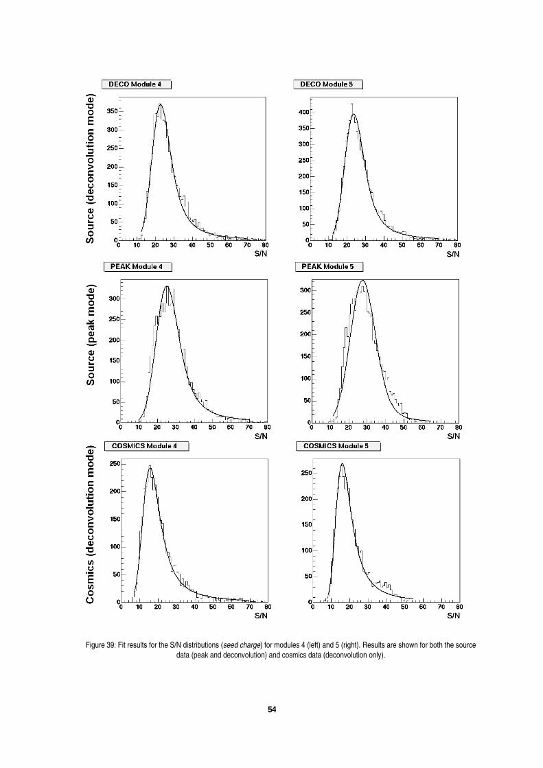
54
Figure 39: Fit results for the S/N distributions (seed charge) for modules 4 (left) and 5 (right). Results are shown for both the source
data (peak and deconvolution) and cosmics data (deconvolution only).

55
Figure 40: Fit results for the cluster signal charge distributions for modules 4 (left) and 5 (right). Results are shown for both the source data (peak and deconvolution) and cosmic data (deconvolution only).

56
Figure 41: Fit results for the S/N distributions (the signal charge distribution is calculated as the cluster signal) for modules 4 (left) and 5 (right). Results are shown for both the source data (peak and deconvolution) and cosmics data
(deconvolution only).

57
8 Noise Occupancy
8.1 Definition The noise occupancy is calculated from pedestal runs and it is defined as the average fraction
of channels read-out due only to noise. The occupancy for channel i and for a given threshold level TH is calculated as the ratio:
( ) [ ]EventsTotal
i
ii
Events
i
iN
CMNTHpedNTHocc
−+≥=
ν
where νi is the digitized charge of channel i, pedi is the mean pedestal for channel i, and CMN is the common mode noise level calculated on an event by event basis.
Equivalently, the noise occupancy can be defined as:
( )( )
∫∞
−+
−−
=CMNTHped
pedx
i
i
i
i
i
edxTHocc2
2
2
2
1 σ
σπ
where σi is the noise of channel i.
Finally, an average on all good strips is performed to obtain the average noise occupancy of the module:
( ) ( )StripsGoodiModule THoccTHocc =
8.2 Results Figure 42 shows the noise occupancies as a function of the threshold level (in ADC counts)
for modules 4 and 5 in both peak and deconvolution modes.
Due to the higher noise level in deconvolution mode, these distributions are wider in deconvolution than in peak mode. For a given threshold level the noise occupancies for deconvolution are thus higher than for peak mode.
9 Signal Efficiency
9.1 Definition The signal efficiency is calculated from the radioactive source data as well as the cosmic ray
data. It is defined, for each channel i and for a given threshold level (TH), as the fraction of clusters where the value of the signal on the seed strip is above this threshold (the signal has already the pedestal subtracted).
The signal efficiency can be written as:
( )ClustersTotal
i
Seed
i
Clusters
i
iN
THSNTHeff
] [ ≥=
where TH is the threshold in ADC counts and Si
Seed is the seed signal cluster charge for channel i.

58
The efficiency for a particular silicon detector module is thus obtained as the average of the above efficiency across all channels of the module. Only those strips not tagged as bad strips are included in the average:
( ) ( )StripsGoodiModule THeffTHeff =
9.2 Results The average efficiencies as a function of threshold (in ADC counts) for modules 4 and 5 are
shown in Figure 43. All results are shown for both source data (peak and deconvolution modes) and cosmic ray data (deconvolution mode only). The statistical uncertainties in all points are calculated from binomial statistics.
Figure 42: Noise occupancy as a function of threshold level for modules 4 (left) and 5 (right). Results are shown for deconvolution
(top) and peak mode (bottom).

59
Figure 43: Signal efficiency as a function of the threshold (in ADC counts) for modules 4 (left) and 5 (right). Results are shown for
source and cosmic data and for peak and deconvolution modes.

60
10 Signal Efficiency vs Noise Occupancy The results of the signal efficiency as a function of the noise occupancy for different threshold
levels are shown in Figures 44-46 for the two modules studied in this report.
From these figures there will be a threshold level which reduces the noise occupancy below a particular value. The signal efficiency could thus be calculated for this threshold and the result used as a figure of merit in grading modules within rods. As long as a threshold is found such that the noise occupancy is below this particular value and the signal efficiency above a certain level, the module can be considered good. This procedure has already been applied in characterizing silicon ISL ladders for the CDF Run II SVX II detector now in operation at the FNAL (Fermi National Accelerator Laboratory, Fermilab) TeVatron collider [7].
Table 8 shows the signal efficiencies calculated for modules 4 and 5 for different noise occupancy values (from the 1σ level to 5σ). Results have been obtained by a linear interpolation to the data shown in Figures 44-46.
In general, for a particular module and noise occupancy value we observe slightly larger signal efficiencies in decovolution mode than in peak mode (from source data only). This is explained by the different noise behavior in these two modes as well as the bias introduced by the S/N threshold cut of the cluster finding algorithm.
The efficiency vs occupancy curves for source and cosmic ray data (taken in deconvolution mode) are nevertheless more similar.
Table 8: Signal efficiencies values (in %) associated to different noise occupancies.
Efficiencies (%)
Occupancies
Source
(peak mode)
Source
(deconv. mode)
Cosmics
(deconv. mode)
1 σ (15.9 %) 100 100 100
2 σ (2.3 %) 100 100 100
3 σ (0.14 %) 98.0 ± 0.3 99.7 ± 0.1 99.9 ± 0.1
4 σ (0.003 %) 94.5 ± 0.3 96.4 ± 0.2 98.6 ± 0.2
MODULE 4
5 σ (0.00003 %) 93.4 ± 0.4 94.8 ± 0.2 97.3 ± 0.3
1 σ (15.9 %) 100 100 100
2 σ (2.3 %) 100 100 100
3 σ (0.14 %) 99.1 ± 0.3 99.9 ± 0.1 99.9 ± 0.1
4 σ (0.003 %) 97.6 ± 0.2 99.2 ± 0.2 99.1 ± 0.2
MODULE 5
5 σ (0.00003 %) 94.6 ± 0.4 98.8 ± 0.2 98.8 ± 0.2

61
Figure 44: Signal efficiency as a function of noise occupancy for different threshold levels. Results are shown for
modules 4 (black points) and 5 (grey points) from beta source data in deconvolution mode. The threshold is the same
for all APVs of the modules and it is varied from 10 to 18 ADC counts above the average pedestal of the chips.

62
Figure 45: Signal efficiency as a function of the noise occupancy for different threshold levels. Results are shown for modules 4
(black points) and 5 (grey points) from beta source data in peak mode. The threshold is the same for all APVs of the modules and it
is varied from 8 to 14 ADC counts above the average pedestal of the chips.
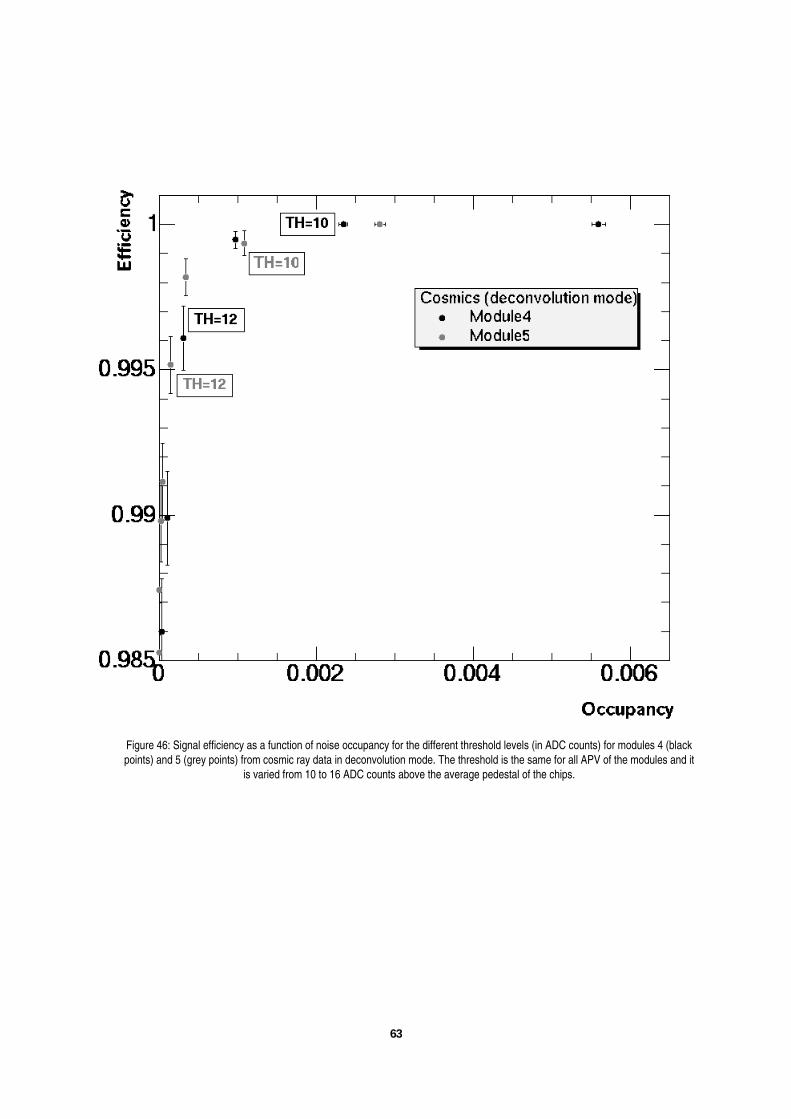
63
Figure 46: Signal efficiency as a function of noise occupancy for the different threshold levels (in ADC counts) for modules 4 (black
points) and 5 (grey points) from cosmic ray data in deconvolution mode. The threshold is the same for all APV of the modules and it
is varied from 10 to 16 ADC counts above the average pedestal of the chips.
64
References on Part 1
1 A PMC based ADC Card for CMS Tracker Readout, J. A. Coughlan. Proceedings of the 5th Workshop on Electronics for LHC Experiments, CERN 99-09, CERN/LHCC/99-33.
The Front-End Driver Card for the CMS Silicon Tracker Readout, J. A. Coughlan. Proceedings of the 8th Workshop on Electronics for LHC Experiments, CERN 2002-003, CERN-LHCC-2002-34, LHCC-G-014.
2 On Calibration, Zero Suppression Algorithms and Data Format for the Silicon Strip Tracker FEDs. I. R. Tomalin. CMS-IN 2001-025.
3 Assembly and Characterization of Cabled Rods During Production at CERN, F. Ahmed, G. Magazzu, J. Valls. CMS Internal Note CMS IN 2003-025. See also: http://cern.ch/valls/CMS_SST/rod_production.html .
XROD - A Program for Rod Characterization and Rod System Tests, J. Valls. CMS Internal Note CMS IN 2003-026.
4 Test of Silicon Detector Modules for the Tracker Endcap with the ARC System. H Axer et al. CMS Note 2003-002.
5 Performance of a CMS Silicon Strip Detector Module with APV25 Read-out. M. Friedl et al. CMS NOTE 2001-038.
6 Energy straggling and Multiple Scattering in Silicon Strip Detectors. S.R Hou et al. Nucl. Instr. and Meth 374 (1996) 309.
Energy loss and energy straggling of protons and pions in the momentum range 0.7 to 115 GeV/c. S. Hancock et al. Phys. Rev. A 28 615 (1983).
7 Production Testing of ISL Modules at FNAL,
T. Affolder et al. CDF note 5180.


66

67
Part 2:
Standalone Software for ATLAS Standalone Software for ATLAS Standalone Software for ATLAS Standalone Software for ATLAS
TileCal ROD Characterization TileCal ROD Characterization TileCal ROD Characterization TileCal ROD Characterization
and System Testsand System Testsand System Testsand System Tests
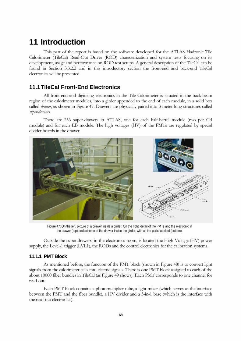
68
11 Introduction This part of the report is based on the software developed for the ATLAS Hadronic Tile
Calorimeter (TileCal) Read-Out Driver (ROD) characterization and system tests focusing on its development, usage and performance on ROD test setups. A general description of the TileCal can be found in Section 3.3.2.2 and in this introductory section the front-end and back-end TileCal electronics will be presented.
11.1 TileCal Front-End Electronics All front-end and digitizing electronics in the Tile Calorimeter is situated in the back-beam
region of the calorimeter modules, into a girder appended to the end of each module, in a solid box called drawer, as shown in Figure 47. Drawers are physically paired into 3-meter-long structures called super-drawers.
There are 256 super-drawers in ATLAS, one for each half-barrel module (two per CB module) and for each EB module. The high voltages (HV) of the PMTs are regulated by special divider boards in the drawer.
Figure 47: On the left, picture of a drawer inside a girder. On the right, detail of the PMTs and the electronic in
the drawer (top) and scheme of the drawer inside the girder, with all the parts labelled (bottom).
Outside the super-drawers, in the electronics room, is located the High Voltage (HV) power supply, the Level-1 trigger (LVL1), the RODs and the control electronics for the calibration systems.
11.1.1 PMT Block
As mentioned before, the function of the PMT block (shown in Figure 48) is to convert light signals from the calorimeter cells into electric signals. There is one PMT block assigned to each of the about 10000 fiber bundles in TileCal (as Figure 49 shows). Each PMT corresponds to one channel for read-out.
Each PMT block contains a photomultiplier tube, a light mixer (which serves as the interface between the PMT and the fiber bundle), a HV divider and a 3-in-1 base (which is the interface with the read-out electronics).

69
Figure 48: On the left, arrangement of a PMT block. On the right, detail pictures of the
photomultiplier (top) and the 3-in-1 board (bottom).
Figure 49: Picture of the optic WLS fibers bundles in a TileCal module connected to the PMTs for their read-out.
11.1.1.1 Photomultipliers
This device is responsible for converting the light signal from the fiber bundles into electric charge. This photomultiplier should be able to work linearly in a wide range, from very low signals (coming from low pT muons) up to the signals coming from very energetic jets. After several studies, the TileCal Collaboration decided to use the Hamamatsu R5900 photomultiplier.
From 2000 to 2003, the Tilecal-Valencia group characterized at and tested at IFIC about 1750 photomultipliers which will be employed in TileCal.
11.1.1.2 Light Mixers
As most of the photomultiplier response depends on the photocathode surface, a light mixing is responsible for mixing the light coming from all the fibers in the bundle, so that there is no correlation between the position of the fiber and the area of the photocathode receiving the light.

70
11.1.1.3 Magentic shielding
The mu metal and iron magnetic shielding in the PMT must prevent residual fields from the ATLAS solenoid and/or toroids from producing gain variations. It should provide a protection up to 500 Gauss magnetic fields in any direction.
11.1.1.4 HV Dividers
The primary purpose of the divider is to partition the high voltage between the dynodes of the PMT. The Tile Calorimeter divider also serves as a socket to allow the connection of the PMT to the front-end electronics without any interconnecting wires. This design minimizes the capacitance between the PMT and the electronics and is important to reduce noise and unreliable connections.
11.1.1.5 3-in-1 Boards
The main functions of this board are: providing a high and a low gain shaped pulse for the digitizer boards, charge injection calibration system and slow integration of the PMT signals for monitoring and calibration.
11.1.2 Digitizer System
Fast pulse signals from the 3-in-1 cards are digitized in digitizer boards and sent down a digital pipeline. On receipt of a LVL1, the digitizer boards capture an event frame consisting of a string of digitizations. The events (data frames) are stored locally and queued for transmission to the Digitizer-to-S-Link interface link. A general diagram for one channel is shown in Figure 50.
Data is presented to the digitizer boards by the 3-in-1 system, which delivers two versions of each signal, a high and a low gain version (being 64 the gain ratio). The data is converted to discrete time format in digitizers formed mainly by commercial ADCs, TTCrx for Trigger and Timing Control (TTC) info receipt and custom ASIC chip TileDMU (Data Management Unit). Samples saturation is the criteria used to decide which set of data (high or low gain) remains.
Figure 50: Digitizer system for a single channel.
The TileDMU (shown in Figure 51) is responsible for reformatting and reordering the digitized data and for sending it to the interface links. Each TileDMU manages 3 ADCs, and each digitizer board has 2 TileDMUs. Therefore there are 8 Digitizer boards for CB superdrawers (up to 48 channels, only 45 are needed), and 6 for EB superdrawers (36 possible channels, only 32 are needed). This configuration can be seen schematically in Figure 50.

71
Figure 51: On the left, digitizers map per drawer in a CB module. On the right, picture of the TileDMU chip.
11.1.3 Digitizer-to-Slink Interface Links
The interface links has two main functionalities:
• Receive the TTC information (two fibers) and send it to digitizers equipped with the TTCrx chip (8 Low Voltage Differential Signaling –LVDS- signals).
• Receive the data (also LVDS) from the up to 8 digitizer boards in a drawer, deserialize them and send it through an optical link to the input stage of the RODs.
The actual design of the interface links is based in S-Link protocol over HP G-Link chips as a physical layer. The implementation is an integrated G-Link Link Source Card (LSC) (640Mbit/s) working at 16 bits in 40 MHz mode (chip HDMP1032). Dual channel read-out is implemented to provide redundancy.
Figure 52: Block diagram for the interface card. Note the redundant read-out from the interface card to the ROD.
11.2 TileCal Back-End Electronics: ROD Crate
11.2.1 Overview Set-up
The RODs [1, 2] will be situated in four crates corresponding to the four read-out partitions (two for the two EBs and two for the CBs). Each partition is managed by the so-called TTC crate and is equipped by standard TTC modules for the LHC experiments.

72
Figure 53: Scheme of the TileCal partitions and the corresponding ROD crates. Note the modules in the ROD
crate in the right-bottom corner.

73
The ROD crate is a standard ATLAS 9U crate. Each ROD crate can hold a crate controller, a Trigger and Busy Module (TBM), and up to 16 ROD motherboards (but at present 8 ROD motherboard are enough for full system read-out in each crate). Each ROD motherboard is associated with a Transition Module. The TileCal partitions and the ROD crate modules (described in the following subsections) are shown Figure 53.
11.2.1.1 Crate Controller
The crate controller is a 6U VME module with a CPU for the initialization of the modules as well as monitoring and support of the VME access (for configuration and data transfer). The VP-110 crate controller from Concurrent Technologies is the standard accepted by the ATLAS collaboration but also a second crate controller is used for tests, the BIT 3 from SBSTM Technologies. A picture of the VP-110 is shown in Figure 54.
11.2.1.2 Trigger and Busy Module (TBM)
The TBM [3] is a 9U VME module which receives trigger signals from the TTC crate. The TBM must be placed in slot #5 in the ROD crate and receives the TTC signals from the trigger system, does the optical to electrical conversion and distributes them to all the ROD modules in the crate through the P3 crate backplane.
Through this P3 backplane, the TBM also receives the 8 ROD Busy signals in the crate and produces a logical OR of these signals to generate a Crate Busy signal. A photo of this module is shown in Figure 55.
11.2.1.3 ROD Motherboard
The ROD motherboard (MB) (Figure 56) is a 9U VME module which can read up to 8 optical fibers from the front-end electronics. It has up to 4 mezzanine cards, called Processing Units, to process the data online before sending it to the Transition Module [4] installed at the back of the VME crate.
11.2.1.4 Transition Module
A picture of this card is shown in Figure 57. These boards are place just behind each ROD module. The ROD module sends the data through the backplane P2 and P3 to the TM which transmits it via optical fibers using up to 4 S-Link mezzanine LSC [5] cards to the Read-Out System (ROS) computer (the next step in the read-out chain). Serializer and deserializer chips are located in ROD and TM respectively to allow this functionality due to the limited number of pins in P2 and custom P3.
Figure 54: VP110 Crate Controller.
Figure 55: Trigger and Busy Module (TBM).
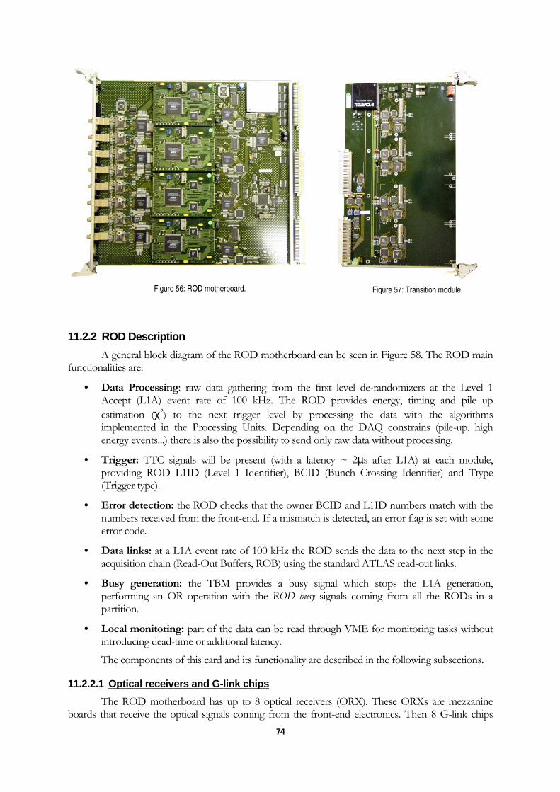
74
Figure 56: ROD motherboard.
Figure 57: Transition module.
11.2.2 ROD Description
A general block diagram of the ROD motherboard can be seen in Figure 58. The ROD main functionalities are:
• Data Processing: raw data gathering from the first level de-randomizers at the Level 1 Accept (L1A) event rate of 100 kHz. The ROD provides energy, timing and pile up estimation (χ2) to the next trigger level by processing the data with the algorithms implemented in the Processing Units. Depending on the DAQ constrains (pile-up, high energy events...) there is also the possibility to send only raw data without processing.
• Trigger: TTC signals will be present (with a latency ~ 2µs after L1A) at each module, providing ROD L1ID (Level 1 Identifier), BCID (Bunch Crossing Identifier) and Ttype (Trigger type).
• Error detection: the ROD checks that the owner BCID and L1ID numbers match with the numbers received from the front-end. If a mismatch is detected, an error flag is set with some error code.
• Data links: at a L1A event rate of 100 kHz the ROD sends the data to the next step in the acquisition chain (Read-Out Buffers, ROB) using the standard ATLAS read-out links.
• Busy generation: the TBM provides a busy signal which stops the L1A generation, performing an OR operation with the ROD busy signals coming from all the RODs in a partition.
• Local monitoring: part of the data can be read through VME for monitoring tasks without introducing dead-time or additional latency.
The components of this card and its functionality are described in the following subsections.
11.2.2.1 Optical receivers and G-link chips
The ROD motherboard has up to 8 optical receivers (ORX). These ORXs are mezzanine boards that receive the optical signals coming from the front-end electronics. Then 8 G-link chips
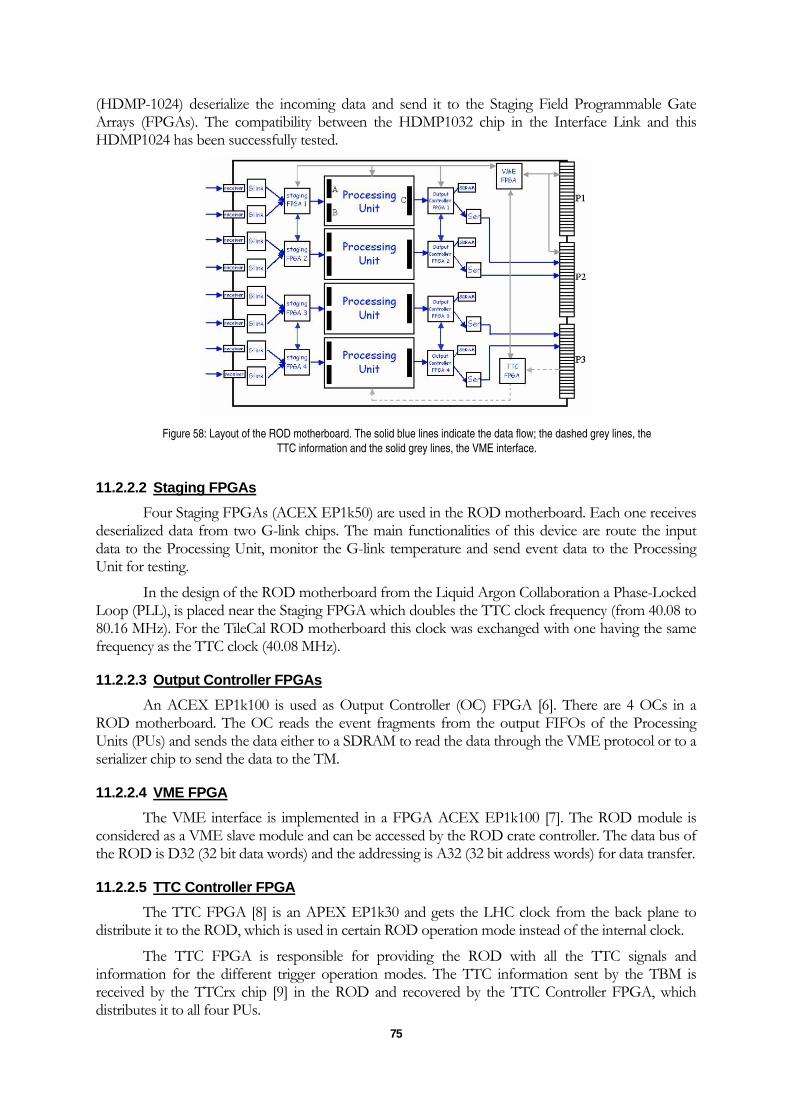
75
(HDMP-1024) deserialize the incoming data and send it to the Staging Field Programmable Gate Arrays (FPGAs). The compatibility between the HDMP1032 chip in the Interface Link and this HDMP1024 has been successfully tested.
Figure 58: Layout of the ROD motherboard. The solid blue lines indicate the data flow; the dashed grey lines, the
TTC information and the solid grey lines, the VME interface.
11.2.2.2 Staging FPGAs
Four Staging FPGAs (ACEX EP1k50) are used in the ROD motherboard. Each one receives deserialized data from two G-link chips. The main functionalities of this device are route the input data to the Processing Unit, monitor the G-link temperature and send event data to the Processing Unit for testing.
In the design of the ROD motherboard from the Liquid Argon Collaboration a Phase-Locked Loop (PLL), is placed near the Staging FPGA which doubles the TTC clock frequency (from 40.08 to 80.16 MHz). For the TileCal ROD motherboard this clock was exchanged with one having the same frequency as the TTC clock (40.08 MHz).
11.2.2.3 Output Controller FPGAs
An ACEX EP1k100 is used as Output Controller (OC) FPGA [6]. There are 4 OCs in a ROD motherboard. The OC reads the event fragments from the output FIFOs of the Processing Units (PUs) and sends the data either to a SDRAM to read the data through the VME protocol or to a serializer chip to send the data to the TM.
11.2.2.4 VME FPGA
The VME interface is implemented in a FPGA ACEX EP1k100 [7]. The ROD module is considered as a VME slave module and can be accessed by the ROD crate controller. The data bus of the ROD is D32 (32 bit data words) and the addressing is A32 (32 bit address words) for data transfer.
11.2.2.5 TTC Controller FPGA
The TTC FPGA [8] is an APEX EP1k30 and gets the LHC clock from the back plane to distribute it to the ROD, which is used in certain ROD operation mode instead of the internal clock.
The TTC FPGA is responsible for providing the ROD with all the TTC signals and information for the different trigger operation modes. The TTC information sent by the TBM is received by the TTCrx chip [9] in the ROD and recovered by the TTC Controller FPGA, which distributes it to all four PUs.

76
11.2.2.6 Processing Units
Online data processing is done by the so-called Processing Units which are 120 × 85 mm mezzanine cards that are connected to the ROD motherboard via 3 connectors. Each ROD motherboard can hold up to 4 PU daughterboards. Nowadays two kinds of PUs are available: the FPGA based PU and the Digital Signal Processor (DSP) based PU.
The FPGA PUs (or dummy PUs) are mainly used for testing purposes and its design is based on a FPGA and two FIFOs. The DSP PUs (also called Final PUs) are more complex with three FPGAs, two DSPs and two FIFOs. Due to the DSPs these PUs can perform digital signal reconstruction. Some algorithms such as Optimal Filtering or Flat Filtering [10] will be implemented in order to calculate energy, time and the quality factor χ2.
The main functions of the FPGA PU are:
• Dataflow management. • Data formatting. • TTC reception. • Buffering and synchronization.
The DSP PU has the same functionalities as the FPGA PU and additionally:
• Data processing with reconstruction algorithms. • Error detection, several checks can be performed like the presence of the start
and the end of an event, the parity of each word, etc.
11.2.2.6.1 FPGA PU
The dummy Processing Unit (or FPGA PU) of the final prototype ROD [1] is a simple board designed to test the ROD in absence of final DSP PU and exploit the FPGA features. It is equipped with two 8 kBytes IDT72V253 FIFOs (the same used for the final DSP PU) and an APEX20KE FPGA, as shown in Figure 59. With this device one can test if the motherboard is able to send data correctly to the PU and if the OC is able to read data from the two FIFOs. Furthermore, DAQ runs can be taken using this dummy PU, although no online energy reconstruction is possible as there are no DSP processors in this device.
11.2.2.6.2 DSP PU
The DSP PU [11] is a more complex device than the dummy PU as it performs digital signal reconstruction. It calculates precisely the energy deposit in the calorimeter cell and the timing of these signals. Moreover it performs monitoring tasks and formats the data for the next element in the electronic chain.
The DSP PU is composed of two blocks, each one with an input FPGA Cyclone EP1C6, a TMS320C6414 DSP from Texas Instruments and an external output FIFO. The DSP PU also contains an output FPGA Cyclone EP1C6 used for the VME and TTC interface. Figure 60 shows a picture of the DSP PU. The input FPGAs and the DSPs can be programmed via VME by uploading the corresponding code through the VME interface.

77
Figure 59: ROD dummy Processing Unit (or FPGA PU). The devices which form the dummy PU are shown on blue
and the LEDs and their functionality in Normal Mode are shown in red.
Figure 60: Picture of the ROD DSP PU with its devices labelled
11.2.3 Installation for ATLAS
In the final ATLAS experiment setup, all the trigger and read-out electronics will be installed in a cavern (USA15) in a radiation free zone, close to the one where the detector will be installed (UX15). USA15 has a two level structure where 238 52U-high racks will be placed. 14 of these racks will be used by TileCal and 2 of them will allocate the RODs. Figure 61 shows the underground structures built for ATLAS, and a detailed view of USA15.
Each rack will contain two 9U ROD crates (with 1 crate controller, 8 RODs, their corresponding 8 TMs and 1TBM) and one 6U TTC crate (equipped with standard ATLAS TTC modules). Figure 62 shows their disposition in the racks.

78
Figure 61: On the left, drawing of the UX15 and USA15 rooms in the underground buildings for ATLAS.
On the right, detail of USA15, and the number of racks that will be placed in each level.
Figure 62: Scheme of the 2 racks which will hold the ROD and TTC crates.

79
11.2.4 System Test Setups
During 2003 and 2004, the ROD Final prototype has been used successfully for data acquisition in the Combined Test Beam (CTB) setup (using dedicated SPS beams to test the performance of all ATLAS detectors in a combined data acquisition; see Section 17.2). Our group also maintains two laboratory setups (in building 5 at CERN and at IFIC-Valencia) were tests with injected data are performed to the ROD prototypes.
The production phase of the RODs will take place in 2005, where all 32 cards will be fully tested and used in the Commissioning setup at the pit, using cosmics. All the TileCal detectors will be placed in UX15 and all the back-end electronics (including the RODs) in USA15. This will be the closest approach to the final ATLAS experiment.
12 Standalone Software for ROD Tests Two different standalone Graphical User Interface (GUI) applications have been developed
for providing intuitive and easy to use tools to test and debug all aspects of the ROD. These two applications are XTestROD and XFILAR.
XTestROD must be run in the ROD Crate Controller and provides access through the VMEbus to the ROD motherboard and the rest of the VME modules placed in the crate (TTCvi, TTCpr, TBM, etc.). XFILAR must be run in the ROS computer to manage the data acquisition cards (FILARs), which are connected to the ROD through optical links.
Both programs use the same hardware and low level software libraries developed in the framework of the Trigger and Data Acquisition (TDAQ) software for ATLAS. The programs XTestROD and XFILAR, together with all the low level libraries developed for the ROD Final and ROD Demonstrator prototypes, have been fully developed by the TileCal-Valencia group.
These applications are designed to be powerful tools for system tests and standalone data acquisition software packages capable of taking data even in long burn-in runs, expected during production. They have been used to qualify pre-production ROD hardware and firmware functionality and to debug the system, in laboratory setups as well as in the 2004 CTB at CERN.
13 Installation and Setup XTestROD and XFILAR are organized as standard CMT packages. These packages have
been compiled using version 3.2 of the gcc compiler and releases 01-00-00 of the ATLAS Dataflow and Online Software. XTestROD also uses the following packages developed by the TileCal-Valencia group:
• rod_demo_rcc
• rod_demo_putius_rcc
• bit3_rcc
• TileVmeROD
The latest stable version of these packages can always be found in the TDAQ CVS repository under the [atlasdaq]/detectors/Tile tree. Detailed information about the software can be found in http://ific.uv.es/tical/rod_new/online_tdaq/index.html.

80
To download the software packages follow the steps described below:
• Configure the following environment variables: export CVSROOT=:ext:atdaq-sw.cern.ch:/atdaqcvs export CVS_RSH=ssh
• To retrieve version vXrYpZ of the package type: cvs –co –r vXrYpZ –d PackageName/vXrYpZ detectors/Tile/PackageName
To compile the software, follow the steps described below:
• Configure the environment variables needed for CMT, Dataflow and Online Software configuration. The XTestROD_HOME and XFILAR_HOME environment variables must also be defined to place the XTestROD and XFILAR configuration files.
• Go to the directory PackageName/vXrYpZ/cmt.
• Type cmt config and source setup.csh for tcsh shell. This will create the compilation and installation scripts and configure some CMT related environment variables.
• Type gmake && gmake install. This will compile and install the PackageName package.
14 Software Development XTestROD and XFILAR have been developed using the Glade interface builder tool and the
related C and C++ code files. Glade is a free program available for all Linux distributions which allows the creation of user graphical interfaces in a visual way. Figure 63 shows the Glade program running and their components.
The main Glade components are the following:
• Glade Main Window: it lists all of the windows and dialogs created in the interface project. By double-clicking on an item in the list the corresponding window or dialog is shown. Menu and toolbar commands enable the developer to create new projects, load and save them and build the source code files.
• Widget Palette: it shows all the available widget for building the interface (windows, dialogs, boxes, buttons, labels, radio buttons, check buttons, etc.). To add new windows and dialogs to the interface, the developer simply selects the icon in the Widget Palette. To add widgets to a window or dialog, the user must select the widget in the palette and click on the position desired for it.
• Property Editor: it allows the developer to change the properties of widgets, such as the widget size or the label text. The Signals tab also allows the developer to add signal handlers to widgets (for example, specify the function to be called when a button is clicked).
• Widget Tree: it shows all the widgets in the interface project and the dependences between them.

81
Figure 63: XFILAR program development using Glade. From left to right, the Glade Main Window, Property
Editor, Widget Tree, Widget Palette and XFILAR interface window can be seen.
Figure 64: XTestROD and XFILAR CMT packages file structure.
Glade generates some files which can be edited and compiled using a standard compiler. XTestROD and XFILAR have been compiled as a CMT package and its file structure is shown in Figure 64. The cmt directory only contains the requirements file, with all the settings for compilation and linking. In the src directory all the source files and its corresponding headers are placed, either created by glade or by the developer. These files are the following:
• PackageName.glade: this is the Glade project file.
• main.cpp: this is the main file for the program. It contains the code needed for windows and dialogs creation and the default startup options.
82
• support.cpp and support.h: these files are created by Glade and should not be edited by the developer. They contain widget related functions.
• interface.cpp and interface.h: these files are created by Glade and should not be edited by the developer. All widgets and signals associated with them are defined in these files.
• callbacks.cpp and callbacks.h: these files are created by Glade and can be edited by the developer at will. Here the developer can write the code functions to be executed for the different widget signals.
• PackageName_main.cpp and PackageName.h: these files were created by the developer for convenience. They are auxiliary files containing functions used during program execution.
• PackageName_utils.cpp and PackageName_utils.h: these files were created by the developer for convenience and contain some basic utilities which are used in the package.
15 Using XTestROD XTestROD is a GUI application written in C and C++ which allows the user to have access
and configure all the ROD crate hardware cards used in TileCal for data acquisition and ROD system tests. All the related registers of these boards can be read and configured from XTestROD. At present, XTestROD may access the following hardware:
• ROD Final motherboard (production board).
• ROD Demonstrator motherboard (prototype board).
• TTCvi
• TTCpr
• TBM
• VMEbus
The XTestROD ROD Demonstrator menu will not be described in this report as it will not be used in further ROD developments. Note that in the final ATLAS setup, the TTCvi will not be placed in the ROD crate, but in the separate 6U TTC crate. However, this card is also placed in the ROD crate in laboratory test setups.
XTestROD must be run in the ROD Crate Controller computer, which provides access through the VMEbus to all the registers in the cards placed in the ROD crate. This way the user can configure intuitively the modules. XTestROD supports the VP-110 and BIT 3 crate controllers.

83
Figure 65: XTestROD Main Window. Note the Hardware Status semaphores in the upper part of the window (in
this case only TTCvi and ROD Final are active).
Figure 66: XTestROD Set Options window.
Figure 65 shows a picture of the XTestROD Main Window. Note that the program version number is displayed in the title bar. By selecting the Set Options menu from the File menu in the menu bar the XTestROD Set Options Window (see Figure 66) appears. From this menu the user must provide the default values used in XTestROD each time it starts. The different settings accessible from the XTestROD Set Options Window are the following:
• Print Command: the default print command.
• Data Path: the directory where the data files taken using XTestROD will be stored3.
• InFPGA Boot File: the default boot file for the Input FPGA in the ROD DSP-PU (see Section 15.3.7.1).
• DSP Boot File: the default boot file for the DSP in the ROD DSP-PU (see Section 15.3.7.1).
3 Make sure the directory specified in the Data Path entry has writing permissions when using XTestROD or XFILAR.
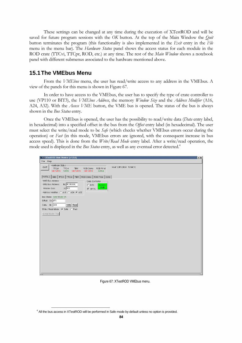
84
These settings can be changed at any time during the execution of XTestROD and will be saved for future program sessions with the OK button. At the top of the Main Window the Quit button terminates the program (this functionality is also implemented in the Exit entry in the File menu in the menu bar). The Hardware Status panel shows the access status for each module in the ROD crate (TTCvi, TTCpr, ROD, etc.) at any time. The rest of the Main Window shows a notebook panel with different submenus associated to the hardware mentioned above.
15.1 The VMEbus Menu From the VMEbus menu, the user has read/write access to any address in the VMEbus. A
view of the panels for this menu is shown in Figure 67.
In order to have access to the VMEbus, the user has to specify the type of crate controller to use (VP110 or BIT3), the VMEbus Address, the memory Window Size and the Address Modifier (A16, A24, A32). With the Access VME button, the VME bus is opened. The status of the bus is always shown in the Bus Status entry.
Once the VMEbus is opened, the user has the possibility to read/write data (Data entry label, in hexadecimal) into a specified offset in the bus from the Offset entry label (in hexadecimal). The user must select the write/read mode to be Safe (which checks whether VMEbus errors occur during the operation) or Fast (in this mode, VMEbus errors are ignored, with the consequent increase in bus access speed). This is done from the Write/Read Mode entry label. After a write/read operation, the mode used is displayed in the Bus Status entry, as well as any eventual error detected.4
Figure 67: XTestROD VMEbus menu.
4 All the bus access in XTestROD will be performed in Safe mode by default unless no option is provided.

85
Figure 68: XTestROD TTCvi menu.
15.2 The TTCvi Menu The TTC-VMEbus Interface (TTCvi) module [12] is a 6U VME card which allows
programmable selection of the trigger source and synchronous signal timing relative to the LHC machine orbit. The main function of the TTCvi is to select a trigger source from either up to four L1A front panel (FP) test trigger inputs, an internal rate programmable random trigger generator or triggers generated by a specific VME access.
In XTestROD, the TTCvi module is handled from the TTCvi menu (Figure 68), where the user has access to the different TTCvi registers. XTestROD handles a single TTCvi card as only one is needed for each ROD crate. At the top of the TTCvi menu window the base VME address register of the module must be set. Once it is initialized with the Access Hardware button, the TTCvi identifiers are automatically shown. The user has the possibility to reset the card, read, write and dump to the screen all the TTCvi registers, which are described in the following subsections.
With the Write All Registers and the Read All Registers buttons all registers are written or read, respectively.
15.2.1 TTCvi L1A Trigger
The L1A Trigger register handles the L1A trigger generation in the L1A Generation box (FP 0 to 3, VME or random) and the L1A random trigger rate in the L1A Random Rate box (from 1 Hz to 100 kHz) in case random trigger is selected from the L1A Generation. The user can also reset the L1A FIFO (L1A FIFO Reset button) and access to the read-only L1A FIFO Empty Flag and L1A FIFO Full Flag.
From this menu one can also generate a single L1A when VME generation is selected as the trigger source (Generate L1A button), enable and disable the trigger word (Enable Trigger Word and

86
Disable Trigger Word buttons) and get the trigger word address, subaddress and external flag parameters (with the Get Trigger Word Param button).
15.2.2 Bunch Crossing and Orbit Register
From this register one can set the source of the orbit generation with the Orbit Generation radio buttons to be internal or coming from FP. The Bunch Crossing delay (expressed in nanoseconds) can also be read (in the BC Delay entry).
15.2.3 Event/Orbit Counter Register
From this register, the user can select the counter register to be either the event or orbit counter (Select Counter radio buttons). The selected (event or orbit) value can also be monitored in the Counter Value entry and the counter can be reset at any time with the Reset Event/Orbit Counter button.
15.2.4 B-Go Channels
In the TTCvi, four VME-addressable FIFOs are provided which may be pre-loaded with commands and data to be transmitted by B Channel cycles. There are thus a total of four B channels. For each of the four channels, the actual transmission of the pre-loaded information is initiated by a signal called B-Go, which can be generated either by writing to VME or by an external signal applied to one of four front panel inputs. It is also possible to start the cycle transmission as soon as the FIFO is not empty. Hence, from the B-Go channels box register, the user can select the mode for the four B-Go channels in the module.
The possible choices for the B-Go mode are FP Enable (enabling external B-Go input), Synchronous (generating a synchronous cycle at the end of the inhibit signal), Single (non repetitive cycles), FIFO (B-Go is generated as soon as the FIFO is not empty) and Calibration Mode (only for channel 2).
15.3 The ROD Final Menu Reference [13] shows a detailed explanation of the low-level library used to access and
configure the ROD motherboard. This library is integrated in the TileVmeROD package.
A view of the panels of the ROD Final menu is shown in Figure 69. In order to access the ROD module, the user has to specify the slot number in the crate where the card is placed and the type of crate controller to use (VP110 or BIT3). With the Access Hardware button, the ROD is initialized and all registers of the different FPGA blocks can then be accessed. There are specific buttons to read all the registers in the menu (Read All Registers) and to write them (Write All Registers). From the ROD Final menu the user may access to the different FPGA blocks of the ROD from a notebook subpanel.
From the Processing Units Booting box panel the user can boot the PUs in the ROD. From PU 1 up to PU 4 option menus the user selects the PU type placed in the corresponding MB slot. The possible choices are Dummy PU (see Section 15.3.6), DSP PU (see Section15.3.7) and Empty (no PU plugged). With the File selection entry buttons the user selects the online software code files to load into the DSP PU Input FPGA (InFPGA File button) and into the DSP (DSP File button). No code needs to be provided for the dummy PU as no booting is needed for this device.

87
Figure 69: XTestROD ROD Final VME Controller menu.
In case the DPS PU is selected, the selected software code is loaded and the PU is booted by clicking on the Boot PUs button. Otherwise, in case the Dummy PU is selected its presence is checked. The corresponding PU indicator turns green if these operations have been successfully performed. More options for DPS PU booting can be found in the DSP Booting submenu of the DSP PU menu (see Section 15.3.7.1).
15.3.1 VME Controller
The VME and Busy FPGA in the ROD MB is responsible for the VME interface between the CPU and the ROD MB, as well as for handling the busy signals at the ROD level5 [7]. The VME Controller submenu describes only the FPGA registers related with the VME communication and is shown in Figure 69.
From this menu the user has access to the Local Register and the IRQ Registers of the VME and Busy FPGA, described in the following subsections. From the Local Register panel, a General Reset command can be sent to the ROD (all the programmable devices will then be reset to their default values). The Force Busy signal, which is activated during ROD initialization in order to avoid incoming triggers, can also be deactivated from this box menu (Deactivate Force Busy button). Note that this line must be deactivated in order to operate the ROD in a normal way. See Section 15.3.2 for more details about busy signal handling in the ROD.
The values of the registers in this menu can always be dumped on the screen using the corresponding Print buttons.
5 Only one FPGA in the ROD motherboard is responsible for the VME controller and the busy registers. However, they have been split into two different menus in XTestROD, according to the functionality instead of the physical device responsible for them.

88
15.3.1.1 Local Register
From the Local Register panel, the base address of the ROD can be read and written (in hexadecimal) and the Board ID can only be read (also in hexadecimal). The Status Register word can also be read as a hexadecimal word. The content of this word register is also shown in detail with bit information about the Force Busy signal state (Force Busy On bit), the number of PUs ready (PU Ready bits), the Extern Data Bus bit and the Quick Answer bit.
15.3.1.2 IRQ Registers
In the ROD there are 6 possible interruption (IRQ) outputs (IRQ1 to IRQ6) with 15 possible interrupt sources: the 8 DSPs, the 4 Output Controllers (OCs), 2 for the busy part and 1 more in case the G-Link temperature exceeds a threshold. Each interrupt source is stored in an Interrupt Request Register (IRR) and then transmitted to an Interrupt Service Register (ISR), which generates the IRQ VME signal.
With the Status Registers the state of the IRQ sources and outputs, as well as the state of the IRRs and ISRs can be accessed by VME. With the Mask/Enable Register the IRQ sources can be masked and the IRQ outputs enabled. With the Reset IRQs button all the requested and pending IRQs are erased from the IRRs and ISRs.
The IRQ registers are not implemented yet in XTestROD.
15.3.2 Busy Registers
In a ROD MB there are 8 busy input signals coming from the PUs (1 per DSP, with 2 DSPs per PU). These busy lines arise when the DSP is not able to accept incoming data, either because it is processing previous data or due to an operation error of the device. The busy lines may also be selected to come from VME (see Figure 71). The busy input signals are logically “Ored” (Busy Or signal), with the possibility to be individually masked. The Busy Out signal, if enabled, drives the busy out and is sent to the TBM through the P3 backplane of the crate and to a LED on the ROD front panel.
After power the card on the Busy Out signal is forced in order to avoid incoming triggers during the ROD initialisation. After startup the user must deactivate the Busy Out line through the Deactivate Force Busy button in the VME Controller submenu (Section 15.3.1). A detailed description of the ROD busy logic can be found in reference [7].
The Busy Registers submenu from the ROD Final menu is shown in Figure 70. From this menu the user can access to the Miscellaneous Register, the Status Register and other busy related timing counters, described in the next subsections. Finally, a pair of buttons in this menu allow the user to send by VME a busy signal (Send BUSY through VME button) and an IRQ signal (Send IRQ through VME button) if the Busy source bit from the Miscellaneous Register is selected to be VME (see below).
The values of the registers and counters in this menu can always be dumped on the screen using the corresponding Print buttons.
15.3.2.1 Miscellaneous Register
The Miscellaneous Register can be written/read as a hexadecimal word or through their individual bits according to their functionality. From this box panel the user can configure the settings for the busy logic in the ROD. This busy operation mode can be selected to be Manual or Normal. The Manual mode is the default after a general reset. In this mode the Busy Out and IRQ signals are disabled (which allows the user to set all registers to the desired values before normal operation). The Normal mode is the operation mode for typical DAQ runs where the busy input signals come from the DSPs in the PUs.

89
With the Busy source bit the user can select the busy source to be either the PUs or VME (it selects thus the input to the busy OR operation, see Figure 71).
Figure 70: XTestROD ROD Final Busy Registers menu.
Figure 71: Busy scheme logic for the ROD.
90
With the Enable Busy and Enable IRQ check buttons the busy and IRQ ROD functionalities can be enabled or disabled by writing into these bits. With the Mask Busy check buttons the user may individually mask the DSPs in order to choose which of them are taken as input to be Ored for the Busy Out signal.
15.3.2.2 Status Register
The Status Register word can be read (in hexadecimal) in this menu and its bit content displayed. From this register, the busy input signal (Busy In) from all DSPs (no matter whether they are masked or not), and the Busy Out (the logical sum of the busy input signals coming from the unmasked DSPs) can be read. The FIFO Full and FIFO Empty flags and the IRQ In and IRQ Out bits are also displayed.
15.3.2.3 Timing counters
Several timing counters can also be read from the Busy Registers submenu. The unit of time in all these counters is chosen by the user in the Clock Divider entry (in hexadecimal). The 40.08 MHz ATLAS clock is thus divided by 4 and by the Clock Divider value.
The Duration Counter entry represents the time during which the ROD has been busy. The value of this counter is written into a FIFO at fixed time intervals (which are set with the Write FIFO Interval entry, in hexadecimal). This FIFO can be read at any time, as well as its FIFO Empty and FIFO Full flags.
The Busy IRQ Counter shows the time that the ROD has been busy since the last reset of the counter. If this value is larger than the Maximum count before IRQ entry (in hexadecimal) an IRQ is sent. All the counters can always be reset either individually (with specific buttons) or in a global way (Reset All Timing Counters button).
15.3.3 Output Controller
The OC FPGA of the ROD is responsible for reading the event fragments from the two output FIFOs associated to each DSP in the PUs. Hence there are four OCs in a ROD motherboard, one per PU. The output data is sent either to a SDRAM memory (to be read using a VME protocol) or to a serializer chip in the ROD motherboard. In this case the data is sent to the ROS through four optical links, using four S-Link Link Source Cards (LSC) in the TM, one per OC. The OC FPGA also formats the event including a header and a trailer and manages the VME request, SDRAM and serializer chips.
The Output Controller submenu of the ROD Final menu is shown in Figure 72. In this menu, after selecting which one of the 4 OCs in the ROD will be configured (Select OC option menu), the user can access to the OC Version, Configuration, Status, SDRAM and Dummy Registers.
The values of the registers and counters in this menu can always be dumped on the screen using the corresponding Print buttons.
15.3.3.1 Configuration Register
With the write/read Configuration Register the user can configure all the parameters related with the output data transmitted with the ROD. The Configuration Register word can be accessed as a hexadecimal word or by its bit functionality. By writing into the Mask PU FIFO check buttons, the 2 FIFOs on the PU corresponding to the selected OC can be masked. If the Enable S-Link check button is set, the data is sent to the S-Link LSC through the TM. Otherwise, the data is stored in the SDRAM. The Data Taking Mode (DTM) check button controls the data flow: when it is set, the data is sent to the SDRAM or to the S-Link; otherwise no data is sent.

91
Figure 72: XTestROD ROD Final Output Controller menu.
Figure 73: Scheme of the OC working in Normal Mode (left) and in Staging Mode (right). Note the different In/Out setting for the two
OCs when working in Staging Mode.
The user can select with the bankmax and rowmax bits the part of the SDRAM to be filled with data6. When the Transfer All check button is deactivated, the word counting and the End of Event word (0xE0E00000) are not transmitted. By setting the Enable Spy bit, one event is stored in the SDRAM for VME read-out and monitoring purposes. See Section 15.4.1 for a detailed description on the correct configuration of the OC bits for a typical data acquisition run.
There is also the possibility with this register to set the OC to operate in Staging Mode7. In this case, the output data from one PU is sent to two OCs instead of one. To configure the OC for working in Staging Mode, the Staging Mode check button must be selected. In case the OC has to deal with data coming from its corresponding PU the In/Out bit must be unset, and set if it has to deal to data coming from the other PU. This bit has no effect if Staging Mode is not enabled.
6 The SDRAM used in the OC has four banks of memory with 4096 rows each. Each row has a capacity of 256 32-bit words. Hence each bank has a capacity of 4 KB. With these bits the user selects up to which bank and row within this bank the SDRAM could be filled with data. 7 Note the difference between the Staging Mode in the OC FPGA and in the Staging FPGA, explained in Section 15.3.5.

92
For convenience, there are buttons in the panel for reading and writing all the bits in this register.
15.3.3.2 Status Register
The read only Status Register contains information about the SDRAM and S-Link status. This register word can be read as a hexadecimal word and its bit contents functionality displayed. The Memory Size entry shows the number of words which are stored in the SDRAM. The Memory Empty flag indicates that no words are stored in the SDRAM. The Memory Full flag shows that the SDRAM has reached its maximum capacity and the Memory Complete flag indicates that the selected capacity with the bankmax/rowmax bits of the Configuration Register has been reached.
Other flags are automatically set when the S-Link fails to pass a test successfully (Link Failure bit) and when no 0xE0E pattern appears in some event (EOE flag bit). These last two flags can be reset independently with the Reset Link and Reset EOE Flag buttons in the main Output Controller submenu. A global OC reset is also possible with the Reset OC button.
15.3.3.3 SDRAM Register
With the SDRAM Register the user has access to the words stored in the SDRAM memory. When the Data Available check button (in the Status Register) is enabled, by reading this register the first word in the SDRAM is read (and removed from the memory).
15.3.3.4 Dummy Register
This is a write/read register used for tests with no relevant information about the status or configuration of the device.
15.3.3.5 Version Register
This is a read only register which contains the OC firmware version number (in hexadecimal) where the first digit represents the version number and the last two the revision number. For example, if the content of this register is 0x320, the firmware version of the OC would be 3.20.
15.3.4 TTC Controller FPGA
The TTC Controller submenu of the ROD Final menu is shown in Figure 74. Here, the user can access to the write/read Version, Control and Dummy Registers and the read only Status Register of the TTC FPGA, which are described in the following subsections. The values of the different registers in this menu can always be dumped on the screen using the corresponding Print buttons.
In addition, with several write only entries the user can provide the Bunch Crossing ID, the Event ID, Trigger Type and the Ttype Sub-Address in a write/read entry when working in VME mode (see below).
15.3.4.1 Control Register
The Control Register word may be accessed in hexadecimal format or by its bit contents. With this register the trigger operation modes of the ROD can be selected with the Trigger Mode radio button. The possible choices are the TTC mode (TTC signals coming from the TTC system), the Local mode (TTC signals come now from a ROD Injector module via an internal ROD connector) and the VME mode (all TTC signals are generated by the VME interface).

93
Figure 74: XTestROD ROD Final TTC Controller menu.
In TTC mode, the clock source must be set to TTC Clock (the clock signal comes from the TTCrx chip). In VME and Local modes the clock source must be MB Clock (with a jumper in the motherboard this clock can be selected to be either a local clock oscillator or a clock signal coming from the ROD Injector via a ROD internal connector).
From this register, the user can also select whether the ROD uses the so called Double L1A Pulse Mode (where the L1A signal will last for two clock cycles instead of one). From specific buttons, one can also reset the TTCrx chip (Reset TTCrx button), reset the event counters in the Status register (Reset Event Counters button), clear the data buffers in the acquisition chain (Flush Buffers, only for VME trigger mode) and clear the Status Register (Clear Status button).
15.3.4.2 Status Register
The Status Register of the TTC FPGA may be read as a hexadecimal word and its bit contents displayed in the panel. From this register the user can check whether the TTCrx chip is ready (TTCrx ready bit) and if the TTC clock is selected and present (TTC Clock Selected and Present bit). There are also in this menu counters for the number of errors in the single or double L1A pulse mode (Single L1A Pulse Mode: Errors and Double L1A Pulse Mode: Errors entries), as well as how many times there has been a non-double L1A trigger when operating in the double L1A pulse mode (Double L1A Pulse Mode: Non double L1A entry).
15.3.4.3 Dummy Register
This is a write/read register used for tests with no relevant information about the status or configuration of the device.

94
15.3.4.4 Version Register
This is a read only register which contains the TTC Controller firmware version number, shown in hexadecimal, where the first digit represents the main version number and the last three digits the revision number.
15.3.5 Staging FPGA
The Staging FPGA is responsible for receiving the incoming data into the ROD from two different G-Link chips and route it to the PU. In Normal Mode operation, the data from two G-Links is sent to a single PU. There is also the possibility to work in the so called Staging Mode8, where the data coming from four G-Links is sent to a single PU (using a bus between each pair of Staging FPGAs). Figure 75 shows a scheme of the ROD operation in Staging Mode.
In addition, a special feature is provided for standalone tests of the ROD. The Staging FPGA has a RAM memory where up to 1024 32-bit words can be stored. The user can now configure the system in order to send this data to the PU, emulating the transmission of events from the FEB.
Figure 75: Scheme of the ROD working in Staging Mode. Note how the output from Staging FPGAs #2 and #4 is sent to the
Processing Unit corresponding to Staging FPGAs #1 and #3, respectively.
The Staging FPGA submenu of the ROD Final menu is shown in Figure 76 and Figure 77. From this menu, the user has access to all the VME configurable registers in the FPGA. In the upper part of the panel the user selects which one of the four Staging FPGAs in the ROD will be accessed with the Select Staging option menu. The version number of the Staging FPGA firmware can be read and printed with the read only Version Register. The other registers in the FPGA are accessed from two different submenus: a Configuration submenu (Figure 76) and a Status submenu (Figure 77).
From the Configuration submenu, the user has access to the write/read Dummy Register, the two Configuration Registers, the Link Configuration Register and the RAM data transmission related registers. On the other hand, in the Staging FPGA Status submenu, the read only Status Register and Temperature Register can be accessed.
The values of all the registers and counters in this menu can always be dumped on the screen using the corresponding Print buttons.
8 Note the difference between the Staging Mode in the Staging FPGA and in the OC FPGA, explained in Section 15.3.3.

95
Figure 76: XTestROD ROD Final Staging FPGA menu: Configuration submenu.
Figure 77: XTestROD ROD Final Staging FPGA menu: Status submenu.

96
15.3.5.1 Configuration Registers
From the Configuration Registers panel, the user can read/write the two Configuration Registers (in hexadecimal) of the FPGA. The registers can be accessed as a hexadecimal word or by its bit functionality.
With these registers, the user can configure the Staging FPGA operation mode. As mentioned before, the ROD can work either in Normal Mode (4 input channels are processed by 2 PUs) or Staging Mode (4 input channels are processed by a single PU); this can be chosen with the Staging Mode bit. When operating in Staging Mode, the output from each Staging FPGA can be routed either to its corresponding PU or to the near PU (see Figure 75). In the first case, the user should check the FEB1 and FEB2 bits in the Enable Output entry, together with the Staging to own PU bit. This configuration is the same when working in Normal Mode. On the contrary, if the Staging FPGA operating in the Staging Mode has to be routed to the PU near its corresponding PU, the user must select instead the FEB1S and FEB2S bits in the Enable Output entry and uncheck the Staging to own PU bit.
In the ROD front panel there is one LED per input optical fiber. There are four possible LED operation modes available in the ROD. The user can select one out of these four modes from the LED Mode entry:
• FEB Mode 1 (normal): the LED is on when an error in the data transmission has occurred (FEB Error, see Section 15.3.5.4). Otherwise, the data link is ready (FEB Link Ready, see Section 15.3.5.4)
• FEB Mode 2: in this mode the LED is on when a Start of Event word is received. This will only be visible with data rates up to 100 Hz.
• RAM Mode: in this mode, the two LEDs associated to the two links of each Staging FPGA indicate when an event is sent from the RAM to the PU (top LED) and when the infinite loop is activated (bottom LED).
• Counter Mode: if events with consecutive words are injected into the ROD, the LEDs operating in this mode indicate when a non consecutive word is received.
The user can also select here whether the FPGA manages incoming FEB data (FEB Data radio button) or sends data from the RAM (DATA RAM radio button). The user can also enable or disable input data from the G-Links to the FPGA with the Disable Input bit.
Finally, the PU not ready bit is related with the PU Ready bit in the Local Register of the VME Controller menu (see Section 15.3.1.1).
15.3.5.2 RAM Data Transmission Registers
The user can select from the Send Events from RAM menu box of the Staging FPGA Configuration panel the number of events to be sent to the PU (Nb of events to send entry) or to send them continuously through an infinite loop (Infinite loop check button). The number of words per event can also be set (Nb of words per event entry) as well as the delay between events in the Delay between events entry (in steps of 25 ns). There is also the possibility to duplicate the data in order to emulate the transmission from two input FEB channels by activating the Control Word check buttons for both FEBs. These control words are needed for the transmission at the PU level. By activating the Enable Busy from DSPs bit, the transmission is stopped when the PU FIFO is full.
From the Configuration panel, the user can also start the transmission of data from the RAM (Start Transmission Data From RAM button), write and read the available data in the RAM (Data to RAM register) and set the address where the first word of the event has to be read (Start Address register).

97
15.3.5.3 Link Configuration Registers
The write/read Link Configuration register must not be edited by the user, as it may have critical consequences for the ROD performance. The default values after a General Reset (issued from the Local Register panel in the VME Controller menu) are those to be used for normal operation of the ROD and data taking.
However, the value of this register can be read/write either as a hexadecimal word or by its bit contents with the corresponding check buttons. The DIV0 and DIV1 entries are used to program the clock divider chain. The FEB 1 Equal and FEB2 Equal bits must be set to 1 if lemo cables are connected to the ROD and to 0 if optical fibers are instead used. The FEB 1 Flag and FEB2 Flag bits must always be set to 1.
15.3.5.4 Status Register
The read only Status Register can be accessed as a hexadecimal word. Its value is shown in the corresponding entry and its bit contents displayed in the panel. The CAV entry lines (Control Available Output) indicate whether the FPGA is receiving data or not, and are used to frame the data. The DAV entry lines (Data Available Output) indicate whether the chip has received data frames. Both entry lines can be read for either FEB 1 or FEB 2. The FEB1 and FEB2 Link Ready signals indicate whether the fibers coming from the drawer are connected with a good communication between them and the ROD. The FEB1 and FEB2 Error signals indicate if an error in the data transmission has occurred. There are also counters for the number of times the FEB Error signal has happened. In addition, there are Internal FIFOs Real Time and Latched Flags entries for the Empty/Full state of the two internal FIFOs defined in the Staging FPGA.
15.3.5.5 Temperature Registers
One of the most critical points of the G-link performance is its temperature [14, 15]. For the TileCal ROD it must not exceed 75°C due to chip specifications. A set of Siemens B57702-M103-G thermistors are placed close to each G-link chip and used to monitor their temperature. The temperature values are read-out by one multichannel MAX1110 ADC, which has eight analog inputs and a serial 8-bit digital output. The output is connected to the staging FPGA number three of the ROD where the current temperature for each G-link chip as well as the minimum and the maximum temperature achieved by each chip since the last reset are stored.
From the Temperature Register menu box the temperature from all eight G-Links can be monitored. The user has to specify the G-Link whose temperature is desired to read in the G-Link Number entry. By clicking on the Read button the corresponding register is read (in hexadecimal) and the Current, Maximum and Minimum temperatures (in Celsius) are displayed in the corresponding entries. The value of the Maximum and Minimum temperatures can always be reset with the Reset button.
15.3.5.6 Dummy Register
This is a write/read register used for tests with no relevant information about the status or configuration of the device.
15.3.5.7 Version Register
This is a read only register which contains the Staging FPGA firmware version number in hexadecimal where the first digit corresponds to the version number and the last three digits to the revision number.
15.3.6 FPGA PU
The FPGA PU submenu of the ROD Final menu in XTestROD is shown in Figure 78 and Figure 79. From this menu the user has access to all VME registers of the FPGA.
98
The user has to select which one of the 4 FPGA PUs in the ROD will be accessed from the Select PU option menu. The FPGA PU menu is divided in two different submenus, each one related with the Configuration (Figure 78) and the Status (Figure 79) FPGA PU registers.
From the Configuration submenu, the write/read Pulse and Set/Reset Busy, Configuration and ROD Output Data Format registers can be accessed. From these registers the user can customize the output data format coming out from the ROD.
From the Status submenu, the read only Status Register, Read Internal FIFO Register, G-Link Counters and Event Counters can be accessed. From this submenu the user can also have access to the write/read Dummy Register.
Additionally in the main FPGA PU menu a read only Version Register and specific buttons to reset the internal and the external FIFOs (Reset Int FIFO and Reset Ext FIFO buttons, respectively), the G-Links (Reset G-Link 1 Stag, Reset G-Link 2 Stag, Reset G-Link 1 and Reset G-Link 2 buttons) and the Latched Flags (Reset Latched Flags button) are provided.
The values of the registers and counters in this menu can always be dumped on the screen using the corresponding Print buttons.
15.3.6.1 Data Format Registers
The ROD Output Data Format registers provide the words which form the header for the two data fragments coming from each G-Link. For a detailed description of the data format see reference [16]. The header words which can be customized are the following:
• Format Version Number: a 32-bit integer number which defines the version number of the ROD data fragment header.
• Source ID for either FEB1 or FEB2: words which identify the source of the fragments. They consist of a subdetector ID, Module Type and Module ID.
• Run Number: a 32-bit integer number which identifies the data run number.
• Extended Level 1 ID: a 32-bit word for the L1ID (Level 1 Trigger ID generated in the TTCrx in ATLAS) identifier (24 lower bits) and the ECR (Event Count Reset, 8 upper bits). This ECR signal resets the 24-bit L1A and increments the 8-bits ECR counter.
• Bunch Crossing ID (BCID): a 12-bit bunch crossing identifier word, generated by the level 1 trigger system in ATLAS.
• Level 1 Trigger Type: an 8-bit word which contains the information sent by the level 1 trigger system about the event type. It is generated by the Central Trigger Processor (CTP) in ATLAS.
• Detector Event Type: identifies the type of the event, which can be either a physics event (if set to 1), a pedestal event (if set to 4), a calibration event from the Charge Injection System (CIS) (if set to 8) or a laser event (if set to 2).
• Number of Words per Event: number of words in each fragment.
• Sub-Fragment ID for either FEB1 or FEB2: 32-bit words which identify each of the sub-fragments associated to each event.

99
Figure 78: XTestROD ROD Final FPGA PU menu: Configuration submenu.
Figure 79: XTestROD ROD Final FPGA PU menu: Status submenu.

100
15.3.6.2 Configuration Register
From the Configuration Register panel the user can read/write the Configuration Register as a hexadecimal word or access it through its bit functionality.
From this register the user can enable or disable the headers of the data coming from each G-Link (Enable PU Header for G-Link/FIFO 1 and 2 check buttons). The format of the headers can be chosen between the following data header format modes:
• BCID, Ttype and Evt ID from VME: the header words for all events are taken from the values provided in the ROD Output Data Format panel, including the BCID, Ttype and Event ID.
• BCID, Ttype and Evt ID from TTC FPGA: in this mode the BCID, Ttype and Event ID words are taken from the TTC FPGA, while the rest from the values provided in the ROD Output Data Format panel.
• BCID from FEB, Evt ID incremented from initial VME value: in this mode the Event ID is incremented event by event from an initial value provided by the user in the ROD Output Data Format panel. The BCID is taken from the FEB and the rest of the header words from the ROD Output Data Format registers.
• BCID from VME, Evt ID incremented from initial VME value: in this mode the Event ID is also incremented event by event from an initial value provided by the user in the ROD Output Data Format panel. The rest of the header words (including the BCID) are taken from the ROD Output Data Format registers.
From the Configuration Register the user can also set the Busy Pulse Length (in units of 25 ns) of the pulse busy signal sent from the PU for test purposes. The dummy PU LED mode can also be selected to be:
• Info displayed in LEDs: the LEDs display information about the Start of Event and the Busy and FIFO state of the two FIFOs in the PU (see Figure 59).
• LEDs in “Knight Rider”: the LEDs display just a flashy side-to-side light (used only for tests).
There is also the possibility to specify in the FEB input entry whether the FEB input going into the PU FIFO is coming from its corresponding Staging FPGA (FEB 1-2 -> FIFO 1-2 radio button) or from it near Staging FPGA (FEB 1-2 S -> FIFO 1-2 radio button).
15.3.6.3 Pulse and Set/Reset Busy Register
With the Pulse and Set/Reset Busy register the user may send an interruption (IRQ 1 and IRQ 2 bits) or a busy signal for debugging purposes. From the Busy 1 and Busy 2 bits, the corresponding FIFO is set to be in busy state. From the Pulse Busy 1 and Pulse Busy 2 bits, the busy signal is send as a pulse with a length specified in the Busy Pulse Length entry of the Configuration Register.
15.3.6.4 Status Register
The read only Status Register can be accessed as a hexadecimal word and its bit contents displayed in the corresponding entries. From this register the user can read whether the PU is working in Staging Mode (Read Staging bit) and access to the Busy and Full/Empty FIFO states of the PU through the Real Time Flags and Latched Flags bits described below.
The Real Time Flags indicate the state of the Busy and FIFOs at the moment the Status Register is read. The Latched Flags indicate whether this state has been reached since the last reset of the ROD (a Latched Flag bit on means that at some instant since the last reset the Real Time flag has been on).

101
There are Real Time Flags and Latched Flags for the External FIFOs Busy signals and the FIFO Empty/Full states. There are also flags for the Almost Full/Empty state, which indicates a FIFO9 memory usage less than 1024 16-bit words for the Almost Empty Flag and more than the total size minus 1024 16-bit words for the Almost Full Flag. By using the Almost Full Flag as a busy signal instead of the Full Flag, a missing event due to lack of memory space in the FIFO is prevented.
For the internal FIFOs in the FPGA there are Real Time Flags for the FIFO Empty/Full states also accessible from this register.
15.3.6.5 Read Internal FIFO
From this panel the user can read the contents of the two internal FIFOs in the FPGA PU (see Figure 59). Each FIFO contains 16-bit words although the contents of both FIFOs are actually displayed as a single 32-bit word.
15.3.6.6 G-Link counters
From this panel the user can read the counters for the number of errors produced in the G-Links data reception. The Link ready entry displays the number of rising edges found in the Link-Ready signal. This signal, sent from the G-Links, indicates that the startup sequence is complete and that data and control indications are valid. Any change in this signal after startup would lead to errors in data reception. The Link errors entry displays the number of times an error has been found in the data, at least in the C-field.
15.3.6.7 Dummy Register
This is a write/read register used for tests purposes with no relevant information about the status or configuration of the device.
15.3.6.8 Version Register
This is a read only register which contains the OC firmware version number (in hexadecimal) where the first digit represents the version number while the last two digits the revision number.
15.3.7 DSP PU
The DSP PU submenu of the ROD Final menu in XTestROD is shown in Figure 80, Figure 81 and Figure 82. From this menu the user can boot the DSP PU and have access to all its VME configurable registers.
The user has to select which one of the 4 DSP PUs in the ROD will be accessed from the Select DSP PU option menu. The DSP PU menu is divided in three different submenus: DSP Booting (Figure 80), Output FPGA (Figure 81) and Input FPGA (Figure 82).
From the Output FPGA submenu, the read only Version and Status registers, the write/read Control, McBSP2 Serial Data and HPI registers can be accessed.
From the Input FPGA submenu, the read only Version Register, the write/read Configuration/Status Register and the write only Programming Register can be accessed.
15.3.7.1 DSP Booting submenu
From this menu the user can select the code files to load into the input FPGA and into the DSP. Here the booting of the DSP PU may also be started. The files containing the software code to be loaded can be selected with the File Selection buttons (InFPGA File button for the input FPGA file and DSP File button for the DSP file). The selected files are displayed in the Selected File labels.
9 The specifications for the Almost Full and Almost Empty states are valid for the FIFO IDT72V253, used in the FPGA PU.

102
The user can boot separately each of the two blocks which compose the DSP PU or both blocks with the DSPs to Boot radio buttons. By clicking the BOOT DSP PU button the selected DSPs and input FPGAs are booted with the corresponding files.
15.3.7.2 Output FPGA submenu
The user must specify which one of the two output FPGAs in the DSP PU will be accessed from the Select OutFPGA option menu. The bit writing operations can be performed in broadcast mode (i.e., write the same bit in both output FPGAs) by activating the Write Broadcast radio button. From this menu the have access to the following registers:
15.3.7.2.1 HPI Register
The Host Port Interface (HPI) is a 16-bit wide bus connected between the DSP and the output FPGA through which the VME can directly access the DSP memory space. It is mainly used for DSP booting, histogram reading and debugging purposes. From the write/read HPI Register entry the user can read data from the DSP or write data into the DSP while it is running.
15.3.7.2.2 McBSP2 Serial Data Register
The Multichannel Buffered Serial port 2 (McBSP2) is a bidirectional serial port which connects the output FPGA and both DSPs. The write/read McBSP2 Serial Data Register is used to exchange data between these devices (send commands to the DSP, read the DSP status, etc.).
15.3.7.2.3 Control Register
The write/read Control Register word may be accessed in hexadecimal format or by its bit contents. From this register the user can reset the DSP (DSP Reset bit) the HPI (HPI Reset bit), the input FPGA (Input FPGA Reset bit) and the corresponding FIFO (FIFO Reset bit). Moreover the user can access to the DSP Launch, HPI Burst and Input FPGA not Config bits.
Figure 80: XTestROD ROD Final DSP PU menu: DSP Booting submenu.

103
Figure 81: XTestROD ROD Final DSP PU menu: Output FPGA submenu.
15.3.7.2.4 Status Register
The read only Status Register can be accessed as a hexadecimal word. Its value is shown in the corresponding entry and its bit contents displayed in the panel. This register contains information about the number of events contained in the McBSO2 FIFO (Nb Events McBSP2 FIFO entry) and in the output FIFO (Nb Events Output FIFO entry), as well as their Empty/Full flags (Output FIFO Flags and McBSO2 FIFO Flag entries). The user can also read in this register the value of the GP11, GP12 and GP13 bits, as well as the HPI INT, HPI Ready, InFPGA Nstatus and InFPGA ConfDone bits.
15.3.7.2.5 Dummy Register
This is a write/read register used for tests with no relevant information about the status or configuration of the device.
15.3.7.2.6 Version Register
This is a read only register which contains the DSP PU output FPGA firmware version number in hexadecimal where the first digit corresponds to the version number and the last digits to the revision number.
15.3.7.3 Input FPGA submenu
The user must specify which one of the two input FPGAs in the DSP PU will be accessed from the Select InFPGA option menu. The bit writing operations can be performed in broadcast mode (i.e., write the same bit in both output FPGAs) by activating the Write Broadcast radio button. From this menu one has access to the following registers:
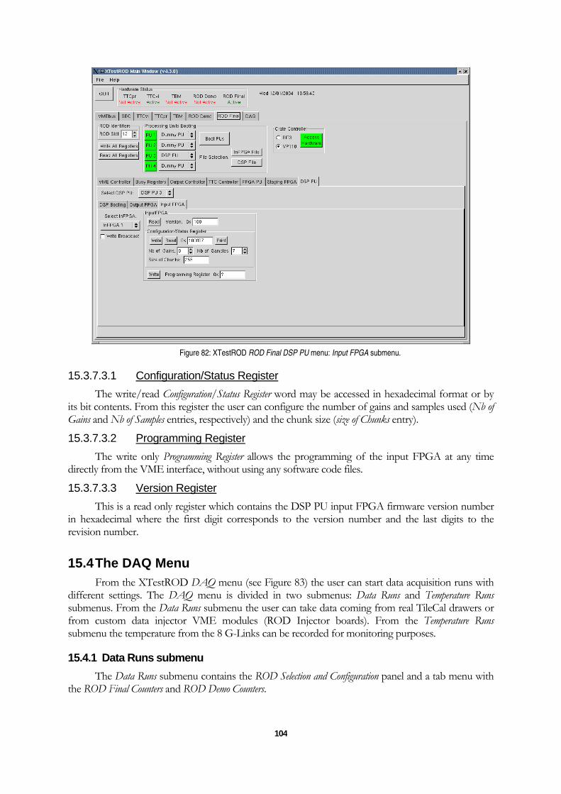
104
Figure 82: XTestROD ROD Final DSP PU menu: Input FPGA submenu.
15.3.7.3.1 Configuration/Status Register
The write/read Configuration/Status Register word may be accessed in hexadecimal format or by its bit contents. From this register the user can configure the number of gains and samples used (Nb of Gains and Nb of Samples entries, respectively) and the chunk size (size of Chunks entry).
15.3.7.3.2 Programming Register
The write only Programming Register allows the programming of the input FPGA at any time directly from the VME interface, without using any software code files.
15.3.7.3.3 Version Register
This is a read only register which contains the DSP PU input FPGA firmware version number in hexadecimal where the first digit corresponds to the version number and the last digits to the revision number.
15.4 The DAQ Menu From the XTestROD DAQ menu (see Figure 83) the user can start data acquisition runs with
different settings. The DAQ menu is divided in two submenus: Data Runs and Temperature Runs submenus. From the Data Runs submenu the user can take data coming from real TileCal drawers or from custom data injector VME modules (ROD Injector boards). From the Temperature Runs submenu the temperature from the 8 G-Links can be recorded for monitoring purposes.
15.4.1 Data Runs submenu
The Data Runs submenu contains the ROD Selection and Configuration panel and a tab menu with the ROD Final Counters and ROD Demo Counters.

105
From the ROD Selection and Configuration panel the user can select which board to be used for data taking (ROD Demo or ROD Final) and the trigger/output configuration. The trigger sources for the ROD can be selected to be VME, TBM and from a front panel (FP). The ROD Final allows also an internal trigger generation in the PU. The selected output data can be:
• VME: the data is read from the SDRAM in the OC as shown in Section 15.3.3.3
• S-Link: the data is sent through the HOLA LSC in the TM to the FILAR PCI cards in the ROS computer.
Only the VME – VME and VME – S-Link modes are implemented for the ROD Demo prototype and the PU – VME and PU – S-Link for the ROD Final.
From the ROD Final Counters and ROD Demo Counters the data acquisition run settings can be configured and the event counters can be read. If ROD Final PU – VME or PU – S-Link modes are selected the user sets which OCs and which of its two FIFOs are enabled for data taking in the Enabled OCs for Test Modes box (of the ROD Final Counters tab menu).
Once all the desired options are selected the user may start an acquisition run by clicking on the Start button. With the Stop button the user can stop the run at any time. The ROD comes back then to its initial state and all the data files are closed.
Figure 83: XTestROD DAQ menu: Data Runs submenu.
15.4.1.1 ROD Final PU – VME test mode
When the PU – VME ROD Final configuration is chosen, the user has to select in the OC counters for PU – VME Mode panel the output data format from the Output file format radio buttons, the counters refreshing mode (Auto or Manual), the VME Write/Read mode and the number of Words to store.
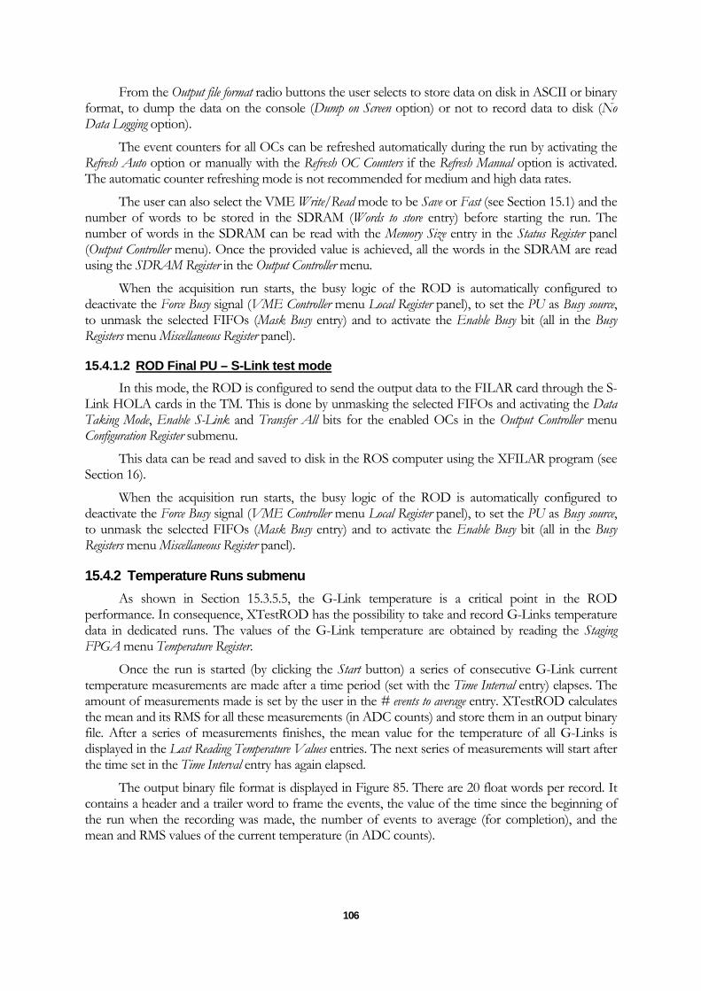
106
From the Output file format radio buttons the user selects to store data on disk in ASCII or binary format, to dump the data on the console (Dump on Screen option) or not to record data to disk (No Data Logging option).
The event counters for all OCs can be refreshed automatically during the run by activating the Refresh Auto option or manually with the Refresh OC Counters if the Refresh Manual option is activated. The automatic counter refreshing mode is not recommended for medium and high data rates.
The user can also select the VME Write/Read mode to be Save or Fast (see Section 15.1) and the number of words to be stored in the SDRAM (Words to store entry) before starting the run. The number of words in the SDRAM can be read with the Memory Size entry in the Status Register panel (Output Controller menu). Once the provided value is achieved, all the words in the SDRAM are read using the SDRAM Register in the Output Controller menu.
When the acquisition run starts, the busy logic of the ROD is automatically configured to deactivate the Force Busy signal (VME Controller menu Local Register panel), to set the PU as Busy source, to unmask the selected FIFOs (Mask Busy entry) and to activate the Enable Busy bit (all in the Busy Registers menu Miscellaneous Register panel).
15.4.1.2 ROD Final PU – S-Link test mode
In this mode, the ROD is configured to send the output data to the FILAR card through the S-Link HOLA cards in the TM. This is done by unmasking the selected FIFOs and activating the Data Taking Mode, Enable S-Link and Transfer All bits for the enabled OCs in the Output Controller menu Configuration Register submenu.
This data can be read and saved to disk in the ROS computer using the XFILAR program (see Section 16).
When the acquisition run starts, the busy logic of the ROD is automatically configured to deactivate the Force Busy signal (VME Controller menu Local Register panel), to set the PU as Busy source, to unmask the selected FIFOs (Mask Busy entry) and to activate the Enable Busy bit (all in the Busy Registers menu Miscellaneous Register panel).
15.4.2 Temperature Runs submenu
As shown in Section 15.3.5.5, the G-Link temperature is a critical point in the ROD performance. In consequence, XTestROD has the possibility to take and record G-Links temperature data in dedicated runs. The values of the G-Link temperature are obtained by reading the Staging FPGA menu Temperature Register.
Once the run is started (by clicking the Start button) a series of consecutive G-Link current temperature measurements are made after a time period (set with the Time Interval entry) elapses. The amount of measurements made is set by the user in the # events to average entry. XTestROD calculates the mean and its RMS for all these measurements (in ADC counts) and store them in an output binary file. After a series of measurements finishes, the mean value for the temperature of all G-Links is displayed in the Last Reading Temperature Values entries. The next series of measurements will start after the time set in the Time Interval entry has again elapsed.
The output binary file format is displayed in Figure 85. There are 20 float words per record. It contains a header and a trailer word to frame the events, the value of the time since the beginning of the run when the recording was made, the number of events to average (for completion), and the mean and RMS values of the current temperature (in ADC counts).
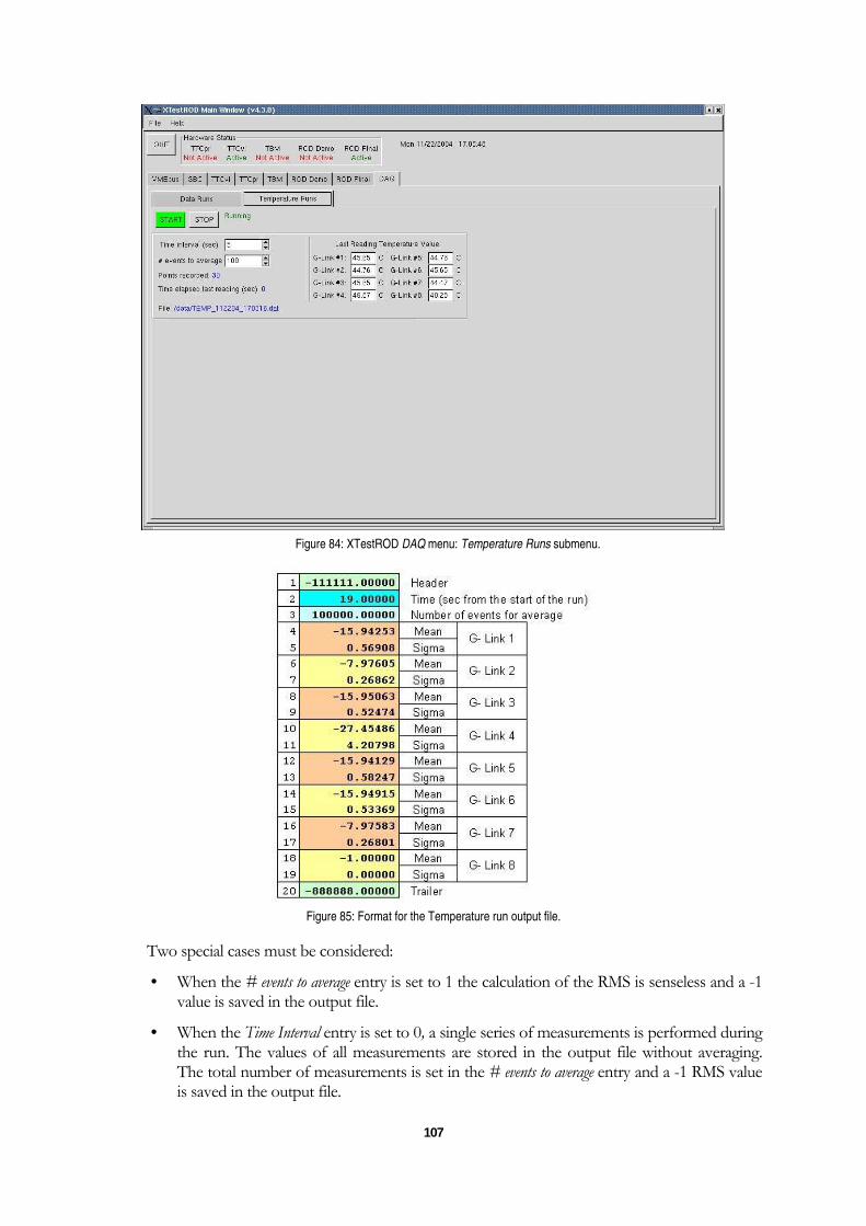
107
Figure 84: XTestROD DAQ menu: Temperature Runs submenu.
Figure 85: Format for the Temperature run output file.
Two special cases must be considered:
• When the # events to average entry is set to 1 the calculation of the RMS is senseless and a -1 value is saved in the output file.
• When the Time Interval entry is set to 0, a single series of measurements is performed during the run. The values of all measurements are stored in the output file without averaging. The total number of measurements is set in the # events to average entry and a -1 RMS value is saved in the output file.

108
Note that during the run the name of the output data file, the number of points recorded and the elapsed time during the last series of measurements are always displayed on the screen.
16 Using XFILAR The FILAR (Four Input Links for Atlas Read-out) [17] is a highly integrated PCI interface card
which can move data from up to four HOLA (High-speed Optical Link for Atlas) S-Link channels to a 32-bit or 64-bit PCI bus running at 33 MHz or 66 MHz. All channels are fully compatible with the HOLA LSC [7] placed at the ROD TM boards. They can receive data at a speed of up to 160 MB/s. The FILAR PCI interface is based on the design of the old S32PCI64 interface.
XFILAR is a standalone GUI application to be run in the ROS computer (where the FILAR cards are installed). The data send from the ROD to the LSC in the TM is received by the Link Destination Channels (LDC) [13] integrated in the FILAR card via optical links. XFILAR controls the FILAR cards in the ROS computer and allows the user to read the data transmitted from the ROD motherboard.
Figure 86 shows a picture of the XFILAR Main Window. From this window the user has access to two different submenu panels, the FILAR menu and the DAQ menu, described below. By selecting Set Options from the File menu in the menu bar, the XFILAR Set Options Window (see Figure 87) appears. From this window the user must provide the default values used in XFILAR each time it starts. The different settings accessible from the Set Options Window are:
• Print Command: the default print command.
• Data Path: the directory where the data files taken using XFILAR will be stored10.
Figure 86: XFILAR main window with the FILAR menu.
10 See footnote #1.

109
Figure 87: XFILAR Set Options menu.
From the DAQ Options in the File menu bar, the DAQ Options window shows up, shown in Figure 88 (this window can also be opened from the Open Run Parameters Window button in the Main Window DAQ panel). Here the user must select the settings related to the data acquisition runs. These parameters are:
• Data Output: the user can select either not to save data to disk (No Data Logging radio button), to dump events on the screen (Dump on Screen radio button) or to save them in a binary or ASCII file (Binary File and ASCII File radio buttons, respectively). The files are created in the path defined in the Set Options dialog with an automatic name which indicates the date and time when the run started.
• Maximum Number of Events per Channel: set the maximum number of events to be stored per channel. Once this limit is achieved, the DAQ run is stopped automatically. By setting the Infinite loop check button an infinite DAQ loop is instead selected and the run can only be stopped manually by the user.
• Refresh Counters: select whether the event and error counters are refreshed either manually or automatically when a new event arrives (not recommended for medium and high rates).
• Check Data Online: if this option is activated, an online checking is performed on the data. This option is meant for checking the correct data transmission from the ROD Injector cards (see Section 17.1.2). If some event containing errors is found, a counter is incremented and the error event and the previous one are written to an ASCII file for a more detailed check.
Figure 88: XFILAR DAQ Options dialog box.
Note that these DAQ settings can always be changed at any time during the execution of XFILAR.

110
At the top of the Main Window, the Quit button exits the program (as with the Exit entry in the File menu) and the Hardware Status entry indicates whether the FILAR cards are being accessed.
16.1 The FILAR Menu From the FILAR menu (Figure 86) the user may select which FILAR cards will be accessed (up
to a maximum of four cards corresponding to a single ROS computer) and which channels of these cards will be enabled (up to four channels per FILAR card).
With the Access Hardware button, all the selected cards are initialized and the selected channels enabled. The page size configuration of the selected FIALR cards (from 256 bytes up to 4 Mbytes) can be set from the Page Size option menu.
The user can always reset at any time any of the FILAR cards (Reset Card buttons) and dump the FILAR information parameters to the console through the Print FILAR Info on Screen button.
16.2 The DAQ Menu From the DAQ menu (Figure 89) the user starts/stops the data acquisition run according to the
settings defined in the DAQ Options dialog window (Figure 88). Once defined the desired parameters for the acquisition, the user starts the run by clicking the Start button. The selected parameters, the number of enabled channels and the event counters are shown in the window (see Figure 89). The Refresh Counters button updates the event counters for the enabled channels.
The DAQ run is stopped when the maximum number of events is achieved or manually at any time with the Stop button.
Figure 89: XFILAR DAQ menu.
17 XTestROD and XFILAR Performance The XTestROD and XFILAR programs have been widely used for several purposes during the
ROD pre-production phase by the TileCal-Valencia group and the rest of the TileCal Collaboration. Some of the aspects where XTestROD and XFILAR have been applied are presented in the following subsections.

111
17.1 ROD Pre-Production Tests XTestROD and XFILAR have been used to test the data flow performance of the ROD in
pre-production tests at the TileCal-Valencia laboratory setups at IFIC and CERN as well as the TileCal Commissioning setups at CERN. These tests can be separated in two different types: output data flow and full input-output data flow tests, which are described in the following subsections.
17.1.1 Output Data Flow Tests
The output part performance of the ROD was tested from the end of 2003 until May 2004 in our laboratory setups by generating data internally in the ROD. Dedicated firmware versions for the dummy PU11 and the Staging FPGA were developed to generate data in a fixed format. This data was then transmitted by the devices downstream to be read-out. Using XTestROD and XFILAR, data files were recorded and later analyzed offline. The main run parameters taken for these tests are described below.
17.1.1.1 Tests Paremeters
• Data Generation: data was generated either in the dummy PU or in the Staging FPGA.
• Data Read-Out: data was read-out either by VME or by S-Link using the FILAR cards (see Section 15.4.1).
• Trigger Rate: data was taken at several trigger rates from 1 Hz up to 100 kHz (the expected maximum L1A trigger rate in ATLAS).
• Data Format: for these tests an easy to check but powerful data format was chosen. A scheme of this data format is shown in Figure 90. It contains all the header and trailer words expected for the final ATLAS data format. The data coming from the FEB input fibers to the ROD is emulated by two blocks of data formed by a repetition of the same word. The upper 4 bits of each word in the block indicate the number of the fiber (0x1 or 0x2 in the scheme in Figure 90) and the lower 28 bits of the word represent a counter which is incremented event by event. Note that the value of this counter is equal in both data blocks.
This format allows to perform the following checks through the data transmission:
• Errors in fixed words (header, trailer, etc…): a change in these words would reveal data corruption.
• Inequality in all the words in a block: this error would be produced if data is corrupted during the transmission.
• Incoherence between the data in each block: this error would imply a loss of one block of data in an event.
• Data blocks non consecutive from previous event: this error could arise if full events are lost during data transmission.
11 The DSP PU has not been used for these pre-production tests as its firmware was not fully developed at the time.

112
Figure 90: Scheme of the data format used for ROD pre-production tests. The two blocks of
data with each FEB fiber output are coloured in yellow and green, respectively.
17.1.1.2 Results
The results of these tests are displayed in Table 9. No transmission errors were found when reading-out through S-Link over a total of about 11×106 events. When reading by VME, errors were found due to the isolated loss of complete events in a ~10-4 ratio in more than 4×10⁶ events, probably due to some synchronisation problem. Note that no data corruption was observed.
It should be mentioned that a 140 Hz maximum transmission rate was obtained when reading-out by VME due to the bus access speed limitation. When the trigger rate exceeds this value, busy signals are produced and the effective rate is reduced to this maximum value.
When reading thought S-Link with the FILAR cards, this maximum transmission rate is observed to be 50 kHz (and only 16 kHz when recording data to disk) even though the ROD must be capable to work up to 100 kHz. A detailed study revealed that this effect was caused by the FILAR cards, which are not capable of accepting such amount of data. Figure 91 shows how the first 4 events are transmitted at a 100 kHz rate, but then triggers are disabled due to a busy signal induced by the FILAR, interrupting the transmission. This shows that the ROD is capable of transmitting data at 100 kHz, although the effective observed rate is of ~16 kHz. However, in the final ATLAS setup, the ROB-In cards (in pre-production phase now) will be used instead of these FILAR cards, and this problem is expected to be solved.
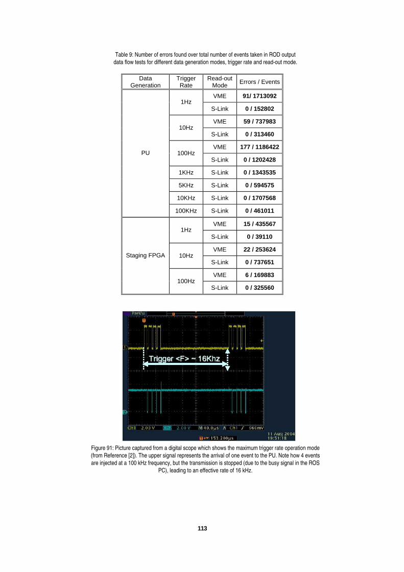
113
Table 9: Number of errors found over total number of events taken in ROD output
data flow tests for different data generation modes, trigger rate and read-out mode.
Data Generation
Trigger Rate
Read-out Mode Errors / Events
VME 91/ 1713092 1Hz
S-Link 0 / 152802
VME 59 / 737983 10Hz
S-Link 0 / 313460
VME 177 / 1186422 100Hz
S-Link 0 / 1202428
1KHz S-Link 0 / 1343535
5KHz S-Link 0 / 594575
10KHz S-Link 0 / 1707568
PU
100KHz S-Link 0 / 461011
VME 15 / 435567 1Hz
S-Link 0 / 39110
VME 22 / 253624 10Hz
S-Link 0 / 737651
VME 6 / 169883
Staging FPGA
100Hz S-Link 0 / 325560
Figure 91: Picture captured from a digital scope which shows the maximum trigger rate operation mode
(from Reference [2]). The upper signal represents the arrival of one event to the PU. Note how 4 events
are injected at a 100 kHz frequency, but the transmission is stopped (due to the busy signal in the ROS
PC), leading to an effective rate of 16 kHz.

114
17.1.2 Full Input-Output Data Flow Tests
Once the output part of the ROD transmission was tested, the next step was to perform full input-output tests, using external sources to inject data. With this, the whole chain from the front-end electronics to the ROS system was tested. These tests were done at the TileCal-Valencia laboratory at CERN and at the Combined Test Beam setup (see Section 17.2) from May to September 2004.
17.1.2.1 Test Paremeters
• Data Source: data was injected from custom 6U ROD Injector boards [18] (shown in Figure 92) which use standard ATLAS Interface Cards (see Section 11.1.3) or directly from the drawers of the modules installed at the CTB setup.
Figure 92: Picture of the ROD Injector board used in the input-output tests equipped with two
standard ATLAS Interface Cards.
• Data Read-Out: due to the amount of data to be tested and the reliability of the system in the output part, only the S-Link read-out was used in this case.
• Data Format: when injecting data from the ROD Injector, the same data format and checks used in the output tests were used (see Section 17.1.1). When using FEB data, the data format is described in Reference 16 (see Figure 93) which differs from the one used at the laboratory.
In this case, the Cyclic Redundancy Check (CRC) and the parity of the words were used to check the data corruption: these quantities are calculated offline and compared with the ones acquired in the FEB data. Any difference would reveal data corruption in the ROD transmission. The words to check in this case are the following:
• CRC16: this word is calculated over each TileDMU packet.
• CRC-CCITT16 (also known as Final Link CRC16): is calculated over the full event fragment, not taking into account the header and trailer words.
• Parity of the words: all the header and data words in all events have a parity bit which was checked in these tests.
17.1.2.2 Results
The first results of these tests revealed data corruption in ~0.5% of the events from both FEB and injected data (see Table 10). After tracing the problem, the error was found to be the loss of 16 bits in the middle of the events, which produced a mismatch between the upper an the lower 16 bits in the 32-bit data words ([19]).
Taking into account the good results of the previous output data flow tests, this problem was clearly located in the input part of the ROD. After several studies (see Reference 2), the cause of theses errors were found to be a firmware problem which was successfully traced and solved.

115
Figure 93: Scheme of the data format used in the CTB data. Note the CRC words for the DMUs and the
Final Link CRC16 word. All the header and data word contains a parity bit which was also checked.
Table 10: Amount and type of errors found for both FEB and injected data in the first input-output data for the tests
performed on ROD prototypes. These errors disappeared later on with updated firmware versions.
FEB Data Injector Data
CRC_CCITT ~0.5% drawers with errors Equality ~0.5% events with errors
CRC_16 ~0.1% DMUs with errors Event order ~0.5% events with errors
Parity ~0.1% words with errors
After this, with stable firmware versions, several (~10) long term runs were acquired (corresponding to a total of 3×10⁹ events) at laboratory and for different trigger rates without data transmission errors. From this, one can estimate that the ROD system has a Bit Error Rate (BER)12 of nearly 6×10-14, which is actually even better than the expected from the G-Link HDMP1024 deserializer chips specifications.
This result was confirmed during the CTB, where the performance of the ROD has been stable and no error or data corruption have been found.
12 The Bit Error Rate is calculated as the number of bits with transmission errors over the total number of bits transmitted by the system.

116
17.1.3 ROD G-Link Temperature Tests at Laboratory
XTestROD has been successfully used to monitor the temperature of the G-Link chips. In Reference [14] a detailed study of the G-Link temperature can be found. As described there, XTestROD has been used to take long G-Link temperature runs (see Figure 94) and this data was used to debug the performance of the G-Link temperature monitoring system which is shown to be very sensitive to noisy power supplies.
Figure 94: Temperature reading of 4 ROD G-Links as a function of time (from Reference [14]). Data was
taken using XTestROD. For each point, 100 events are acquired and their mean calculated. Error bars
represent the temperature standard deviation over 100 readings.
17.1.4 Debug During ROD Firmware Development
During all the ROD FPGAs firmware development procedure the different firmware versions have been debugged and tested using XTestROD and XFILAR.
17.2 Integration at the Combined Test Beam Setup The CTB program took place from May to November 2004 at CERN. It consists in data
acquisition runs using dedicated SPS secondary beams (electron, pion, muon and photon beams) with all the ATLAS sub-detectors in a combined way. The main goal of this program is to integrate all sub-detectors and integrate them with the TDAQ environment. In the CTB a common trigger and DAQ was used, as well as a combined monitoring, reconstruction and simulation software (using Geant4) based in the Athena framework. This has been the closest approach to the final ATLAS setup using final or almost final front-end and back-end electronics.
Figure 95 shows a scheme of all the subdetectors placed in the beam line in the same disposition as they will be in ATLAS (from upstream to downstream: Pixel, SCT, TRT, LAr –in its cryostat-, TileCal and muon chambers). Figure 96 shows a picture of the setup with the different subdetectors.

117
Figure 95: Scheme of the disposition of the ATLAS subdetectors in the CTB setup.
Figure 96: Picture of the CTB with some of the subdetectors labelled.
At the CTB studies with various subdetectors were made: combined electromagnetic and hadronic calorimetry (resolution, energy sharing, linearity, etc.), inner detector (tracking and particle identification), inner detector and muon tracking, calorimeter and muon performance, etc. These studies will be used to tune the Monte Carlo simulations before the final ATLAS commissioning (note that similar studies can only be possible after CTB with cosmics in the experiment cavern or directly in the first LHC collisions.).
As for the TileCal, three CB and three EB modules were installed, with a total of 9 superdrawers for read-out. As for the back-end electronics, one ROD equipped with 3 dummy PUs was installed at the CTB to read up to 6 drawers, which belonged to CB and/or EB modules depending on the needs. XTestROD and XFILAR together with the TileVmeROD library have been employed to integrate the ROD in the TDAQ environment. The performance of the ROD (after the firmware problems mentioned above were solved) was stable and without data transmission errors.
17.3 Pre-ROD Board Debug and Development As mentioned in Section 11.1.3, TileCal is a redundant acquisition system: two fibers carry the
same data from the Interface Cards to the ROD. In such a radiation hard environment and in a long-lived experiment as ATLAS, this redundancy is mandatory in order to prevent the effect of the malfunctions in the front-end electronics due to radiation damage.

118
Figure 97: Picture of the 6U Pre-ROD OMB prototype.
To exploit this redundancy, a Pre-ROD Optical Multiplexer Board (OMB) is being developed by the DSDC group at the Universitat de València Dpt. Ingeniería Electrónica. This 9U board will receive the two fibers carrying the same data, check possible errors in them and provide the correct one to the ROD as input. In another operation mode, this module will generate data so that it may also be used as ROD Injector.
Figure 98: XTestROD Pre-ROD Prototype menu (in development at the moment)
The OMB first 6U prototype (shown in Figure 97) construction is finished and it has been tested and debugged from summer 2004 at out laboratory setups at Valencia and at CERN. XTestROD and XFILAR have been the tools used to perform DAQ runs and check the quality of the data transmitted adding this Pre-ROD board to the read-out chain. Moreover, further developments in XTestROD will include specifically a menu for the Pre-ROD module with all the VME registers of the board (see Figure 98).

119
120
References on Part 2
1 TileCal ROD Hardware and Software Requirements. J. Castelo et al., December 2004. ATLAS Note ATL-TILECAL-2005-003.
The ROD Mother Board for the ATLAS Liquid Argon Calorimeter. A. Blondel, D. La Marra, A. Léger, I. Riu, A. Straessner. June 2004. ATLAS EDMS document ATL-AL-EN-0055.
2 Tile Calorimeter Read Out Driver. Firmware Developments for the Final Prototype. J. Castelo. September 2004. Proceedings of LECC 2004.
3 The Trigger and Busy Module of the ATLAS LARG ROD System. P. Matricon. June 2004. ATLAS EDMS document ATL-AL-EN-0054.
4 A 9U Transition Module for the ROD Demonstrator. P. Matricon. June 2004. ATLAS EDMS document ATL-AL-EN-0053.
5 HOLA High-speed Optical Link for ATLAS. A. Ruiz, E. van der Bij, June 2002. ATLAS EDMS document 330901.
6 OC (Output Controller) FPGA of the LArgROD board Description. D. La Marra. April 2004. ATLAS EDMS document ATL-AL-EN-0056.
7 VME and BUSY FPGA for the ROD motherboard. A. Blondel, D. La Marra, A. Léger, I. Riu, A. Straessner. December 2003. ATLAS EDMS document ATL-AL-EN-0060.
8 TTC FPGA Version 2.00. G.Perrot , F. Corageoud. September 2003. http://dpnc.unige.ch/LArgROD/TTC_FPGA2_00.pdf.
TTC System Implementation for ATLAS Liquid Argon Detectors. Laforge, B; Perrot, G. April 2004. ATL-ELEC-2004-003.
9 TTCrx reference Manual. J. Christiansen, A. Marchioro, P. Moreira and T. Toifl. January 2003. http://ttc.web.cern.ch/TTC/TTCrx_manual3.8.pdf.
10 Optimal Filtering in the ATLAS Hadronic Tile Calorimeter. E. Fullana et al. January 2005. ATLAS Internal Note ATL-TILECAL-2005-001.
11 The TMS320C6414 DSP Mezzanine board. J. Prast. August 2004. ATLAS EDMS document ATL-AL-EN-0051.

121
12 TTC-VMEbus INTERFACE TTCvi – MkII. Ph. Farthouat, P. Gällnö. May 2000. Rev 1.6, RD12 project, CERN. ATLAS EDMS document 110746.
TTCvi Library for ROD Crate DAQ. R. Spiwoks. February 2003. ATLAS EDMS document ATL-D-ES-0012.
13 TileCal ROD Motherboard Software Library - User's Manual. B. Salvachúa. October 2004. ATLAS Communication ATL-COM-TILECAL-2005-004, waiting for ATLAS Note approval.
14 A. Ruiz-Martinez, A. Munar et al. ATLAS Note in preparation.
15 The ATLAS LARG ROD G-Links Cooling System. F. Hubaut, B. Laforge, P. Repain, F. Rossel, D. Vincent. March 2004 ATL-ELEC-2004-002.
16 The raw event format in the ATLAS Trigger & DAQ. C. Bee, D. Francis, L. Mapelli, R. McLaren, G. Mornacchi, J. Petersen, F. Wickens. February 2004. ATLAS Communication ATL-DAQ-98-129. EDMS document ATL-D-ES-0019.
The Output Dataformat For RODfinal in ATLAS Combined Testbeam. J. Castelo, July 2004. Unpublished internal document.
TileCal ROD data format (2004 version). http://tilde-solodkov.home.cern.ch/~solodkov/ROD_format.html.
17 FILAR. Quad HOLA S-LINK to 64-bit/66 MHz PCI Interface. Users Guide. E. van der Bij, W.Iwanski, M. Joos. May 2002. ATLAS EDMS document 337904.
The FILAR driver and library. M. Joos. December 2002. ATLAS EDMS document ATL-D-ER-0004.
18 ROD VME Injector motherboard. Description Manual. J. Castelo. May 2004. Draft document available at http://ific.uv.es/tical/rod/rodinj/doc/RODVME_inj.pdf.
19 Functionality and system Tests Results of Production Protoype RODs. J. Poveda. Talk given TileCal Electronics Engineering meeting. CERN, 18 June 2004.

122

123
CONCLUSIONSCONCLUSIONSCONCLUSIONSCONCLUSIONS

124

125
18 Conclusions In this report two different tasks done in different experiments and different subdetectors
(Tracker Outer Barrel, TOB, in the CMS Silicon Strip Tracker, SST, and Hadronic Tile Calorimeter, TileCal, in the ATLAS calorimetry) have been presented.
The first part is framed in the CMS silicon TOB detector. The work is based in the contribution to the validation of the silicon modules and the study of the performance of their mechanical holding structures during the pre-production phase. Here, data from TOB prototype double sided rods with final components in a system test setup at CERN have been analysed in terms of noise and signal performance for different APV read-out chip operation modes (deconvolution and peak modes).
Pedestal runs data has been used for noise studies. In APV deconvolution mode channel noise averages have been found to be ~25% larger than in peak mode, as expected from the chip design. Individual channel noise has been used to identify bad behaviour strips in the modules, which have not been taken into account in further analysis.
Beta source and cosmics runs data has been used for signal to noise ratios studies. Signal to noise ratios of ~15 and ~25 have been found for APV deconvolution and peak mode respectively, in agreement with previous test beam studies.
In addition, signal efficiencies and noise occupancies have been calculated for several thresholds. They have been proposed to be used in a combined way as a function of merit for grading the silicon modules in terms of their performance during production. Signal efficiencies over 98% have been found for a 0.14% noise occupancy level for all the modules and chip read-out modes studied.
The second part of this work is framed in the ATLAS TileCal detector and the work is based in the ROD final prototype development and pre-production. In this part two graphical user interface applications called XTestROD and XFILAR have been presented. These programs are tools to test in detail the performance of the ROD, its FPGAs and related components. They have been widely used by the TileCal Valencia group and other members of the TileCal collaboration in the pre-production, test beam and commissioning phases of the detector. In particular they have been used to debug and test the following aspects of the ROD and related back-end boards:
• Hardware: all the hardware functionality of the ROD system has been tested with XTestROD and XFILAR. Possible malfunctions in the boards would be detected using these programs.
• Firmware: the firmware developed for the ROD FPGAs has been fully tested with these programs.
• Software: XTestROD have been used to test all the methods developed for the ROD in the TileVmeROD library.
XTestROD and XFILAR have been the tools used for data acquisition in output and input-output data flow tests at laboratory. In these tests, more than 3×10⁹ events have been acquired through S-Link in long runs without data transmission errors, achieving a Bit Error Rate of ~6 ×10-14.
In addition, these programs will also be used during the ROD production phase (from April to July 2005) for debugging any problematic board, as well as in further development in trigger synchronisation and DSP performance.

126

127


129
Appendix I: Acronym list
ADC Analog to Digital Converter ALICE A Large Ion Collider Experiement AOH Analog OptoHybrids APV Analog Pipeline Voltage mode chip ASCII American Standard Code for Information Interchange ASIC Application-Specific Integrated Circuit ATLAS A Toriodal LHC AparatuS BC Bunch Crossing BER Bit Error Rate BT Barrel Toroid (ATLAS Magnet System) CAV Control Available Output CB Central Barrel CCUM Control and Communication Unit Module CERN Conseil Européen pour la Reserche Nucléaire (European Council for the
Nuclear Research) CKM Cabibbo-Kobayashi-Maskawa, matrix for quark mixing CMN Common Mode Noise CMS Compact Muon Solenoid CMS-like noise Common Mode Subtracted noise CMT Configuration Management Tool CNGS CERN Neutrinos to Gran Sasso CS Central Solenoid (ATLAS Magnet System) CSC Cathode Strip Chamber (CMS and ATLAS Muon Detector) CTB Combined Test Beam CVS Concurrent lersión System DAQ Data AcQuisition DAV Data Available Output DMU Data Management Unit DONUT Direct Observation of the NU Tau, experiment at FNAL DS Double Sided DSP Digital Signal Processor DT Drift Tubes (CMS Muon Detector) DTM Data Taking Mode EB Extended Barrel ECAL Electromagnetic CALorimeter (CMS) ECT EndCap Toroids(ATLAS Magnet System) EDMS Engineering Data Management Service EM Electromagnetic EMEC EM EndCap (ATLAS EM Calorimetry) EWSB ElectroWeak Symmetry Breaking FCAL Forward CALorimeter (ATLAS Hadron Calorimetry) FEB Front-End Boards FEC Front-End Control FED Front-End Driver

130
FIFO First Input First Output memory FILAR Four Input Links for ATLAS Read-out FNAL Fermi National Accelerator Laboratory FP Front Panel FPGA Field Programmable Gate Array FWHM Full Width at Half Maximum GUI Graphical User Interface HB Hadron Barrel (CMS HCAL) HCAL Hadronic CALorimeter (CMS) HE Hadron Endcap (CMS HCAL) HEC Hadronic EndCap (ATLAS Hadron Calorimetry) HF Hadron Forward (CMS HCAL) HOB Hadron Outer Barrel(CMS HCAL) HOLA High-speed Optical Link for ATLAS HPI Host Post Interface HV High Voltage ID Inner Detector (ATLAS) IFIC Institut de Física Corpuscular IRQ Interruption Request IRR Interrupt Request Register ISOLDE Isotope separation OnLine Device ISR Intersecting Storage Rings ISR Interrupt Service Register L1A Level 1 Accept LAr Liquid Argon LDC Link destination Channel LEP Large Electron-Positron collider LHC Large Hadron Collider LHCb Large Hadron Collider beauty LSC Link Source Card LVDS Low Voltage Differential Signal LVL1 LeVeL 1 MB MotherBoard McBSP2 Multichannel Buffered Serial Port 2 MDT Monitored Drift Tube (ATLAS Muon Detector) MIP Minimum Ionizing Particle NIM Nuclear Instrument Module OC Output Controller OMB Optical Multiplexer Board ORX Optical Receiver PCI Peripheral Component Interconnect, computer bus standard PMC PCI Mezzanine Card PMT PhotoMultiplier Tube PPL Phase-Locked Loop PU Processing Unit QCD Quantum Chromodymanics RCC ROD Crate Controller ROB Read-Out Buffers ROD Read-Out Driver ROS Read-Out System RPC Resistive Parallel Chamber (CMS Muon Detector)

131
S/N Signal over Noise ratio SCT SemiConductor Tracker (ATLAS ID) SDRAM Synchronous Dynamic Random Access Memory SLAC Stanford Linear Accelerator Center SLC Stanford Linear Collider SM Standard Model SPS Super Proton Synchrotron SS Single Sided SST Silicon Strip Tracker TBM Trigger and Busy Module TDAQ Trigger and Data Acquisition TEC Tracker EndCap (CMS Tracker) TGC Thin Gap Chamber Tube (ATLAS Muon Detector) TH Threshold TIB Tracker Inner Barrel (CMS Tracker) TID Tracker Inner Disk (CMS Tracker) TileCal Tile calorimeter (ATLAS Hadron Calorimetry) TM Transition Module TOB Tracker Outer Barrel (CMS Tracker) TRT Transition Radiation Tracker (ATLAS ID) TSC Trigger Sequence Cards TTC Trigger and Timing Control TTCrx TTC Receiver TTCvi TTC VMEbus Interface UTRI Ultima Tracker Read-out Interface VME Versa Modula Europa bus WLS WaveLength Shifter


133
Appendix II13: From Standard Model Physics to LHC. A brief review of High Energy Physics in the last years and the nearest future.
The Standard Model (SM) is a very successful description of the interactions of the
components of matter at the smallest scales (<10-18 m) and highest energies (~ 200 GeV) available. It is a quantum field theory which describes the interaction of spin-1/2, point-like fermions, whose interactions are mediated by spin-1 gauge bosons. The bosons arise when local gauge invariance is applied to the fermion fields, and are a manifestation of the symmetry group of the theory, which for the standard model is SU(3) × SU(2) × U(1). The fundamental fermions are leptons and quarks. There are three generations of fermions, each identical except for mass. The origin of this generational structure, and the breaking of generational symmetry (i.e. the different masses of each generation) remains a mystery. Corresponding to the three generations, there are three leptons with electric charge -1, the electron (e), the muon (µ) and the tau (τ), and three electrically neutral leptons (the neutrinos νe, νµ and ντ). Similarly there are three quarks with electric charge +2/3, up (u), charm (c) and top (t), and three with electric charge -1/3, down (d), strange (s) and bottom (b). There is mixing between the three generations of quarks, which in the SM is parametrized (but not explained) by the Cabibbo-Kobayashi-Maskawa (CKM) matrix.
The quarks are triplets of the SU(3) gauge group and so they carry an additional "charge", referred to as color, which is responsible for their participating in the strong interaction (quantum chromodynamics or QCD). Eight vector gluons mediate this interaction; they carry color charges themselves, and are thus self-interacting. This implies that the QCD coupling αS is small for large momentum transfers but large for soft processes, and leads to the confinement of quarks inside color-neutral hadrons (like protons and neutrons). Attempting to free a quark produces a jet of hadrons through quark-antiquark pair production and gluon bremsstrahlung.
In the SM, the SU(2) × U(1) symmetry group, which describes the so-called Electroweak Interaction, is spontaneously broken through the existence of a (postulated) Higgs field with non-zero expectation value. This leads to the emergence of massive vector bosons, the W± and the Z, which mediate the weak interaction, while the photon of electromagnetism remains massless. One physical degree of freedom remains in the Higgs sector, which could be manifest most simply as a neutral scalar boson H0, which is presently unobserved.
The basics of the SM were proposed in the 1960's and 1970's. Increasing experimental evidence of the correctness of the model accumulated through the 1970's and 1980's. Deep inelastic scattering experiments at SLAC showed the existence of point-like scattering centers inside nucleons, later identified with quarks. The c and b quarks were observed and neutral weak currents (Z exchange) were identified. Three-jet final states (from gluon bremsstrahlung) were observed in e+e- and hadron-hadron collisions, and the W and Z were directly observed at the CERN SPS collider. Following these discoveries, the 1990’s decade was largely an era of consolidation. Even more precise experiments were carried out at LEP and SLC which provided verification of the couplings of quarks and leptons at the level of 1-loop radiative corrections - O(10-3). The top quark was discovered at FNAL in 1995, and it was found to have an unexpectedly large mass (175 GeV). After the discovery in 2000 of the ντ in the DONUT experiment also at FNAL, only one particle of the SM has yet to be observed: the
13 Adapted from CMS HCAL Technical Design Report, Section 1.2.

134
Higgs boson. The last, but the most important as it holds the key to the generation of W, Z, quark and lepton masses.
The successes of the Standard Model have drawn increased attention to its limitations. In its simplest version, the SM has 19 parameters - three coupling constants, nine quark and lepton masses, the mass of the Z boson which sets the scale of the weak interaction, four CKM mixing parameters, and one (small) parameter describing the scale of CP violation in the strong interaction. The remaining parameter is associated with the mechanism responsible for the breakdown of the electroweak SU(2) × U(1) symmetry to U(1) of electromagnetism ("electroweak symmetry breaking" or EWSB). This can be taken as the mass of the Higgs boson the couplings of the Higgs are determined once its mass is given. Within the model we have no guidance on the expected mass of the Higgs boson. The current experimental lower bound from LEP2 is about 115 GeV, and the upper limit from global fits to electroweak parameters is about 470 GeV. As its mass increases, the self-couplings of the W and Z grow, and so the mass must be less than about 800 GeV, or the strong dynamics of WW and ZZ interactions will reveal new structure. It is this simple argument that sets the energy scale that must be reached to guarantee that an experiment will be able to provide information on the nature of electroweak symmetry breaking, which is the central goal of the Large Hadron Collider.
The presence of a single elementary scalar boson is distasteful to many theorists. If the theory is part of some more fundamental theory with a larger mass scale (such as the scale of grand unification, or the Planck scale) then radiative corrections will result in the Higgs mass being driven up to this large scale unless some delicate cancellations are engineered. There are two ways out of this problem which both result in new physics on the scale of 1 TeV. New strong dynamics could enter that provide the scale of the W mass or new particles could appear which would cancel the divergences in the Higgs boson mass. In any of these eventualities - standard model, new dynamics or new particles - something must be discovered at the TeV scale, i.e. at the LHC.
Supersymmetry is an appealing concept for which there is at present no experimental evidence. It offers the only presently known mechanism for incorporating gravity into the quantum theory of particle interactions and provides an elegant cancellation mechanism for the divergences affecting the Higgs mass, while retaining all the successful predictions of the standard model and allowing a unification of the three couplings of the gauge interactions at a high scale. Supersymmetric models postulate the existence of superpartners for all the presently observed particles. There are bosonic superpartners of fermions (squarks and sleptons), and fermionic superpartners of bosons (gluinos and gauginos χi
0, χi±). There are also multiple Higgs bosons: h, H, A and H±. There is thus a
large spectrum of presently unobserved particles, whose exact masses, couplings and decay chains are calculable in the theory given certain parameters. Unfortunately these parameters are unknown; but if supersymmetry has anything to do with EWSB, the masses should be in the region 100 GeV - 1 TeV.
An example of the strong coupling scenario is "technicolor" models based on dynamical symmetry breaking. An elegant implementation of these ideas is lacking. Nonetheless, if the dynamics has anything to do with EWSB, we would expect new states in the region 100 GeV - 1 TeV. Most models predict a large spectrum. At the very least, there must be structure in the WW scattering amplitude at around 1 TeV center of mass energy.
There are also other possibilities for new physics that are not necessarily related to the scale of EWSB. There could be neutral or charged gauge bosons with masses larger than the Z or W. There could be new quarks, charged leptons or massive neutrinos or quarks and leptons might turn out not to be elementary objects. While we have no definite expectations for the masses of such particles, the LHC must be able to search for them over its entire available energy range.

135
Appendix III: Definition of some physical magnitudes
• Pseudorapidity (ηηηη): This is an angular variable defined by:
( )( )2tanlog θη −=
whose inverse function is:
( )ηθ −−= e1tan2
where θ is the angle between the particle considered and the undeflected beam. Figure 99 shows the relation between both angular variables graphically.
Figure 99: Pseudorapidity (η) as a function of the angle θ (in degrees).
• Radiation length (x0): Scale variable appropriate for describing high-energy electromagnetic shower which can be defined either as the mean distance over which a high-energy electron loses all but 1/e of its energy by bremsstrahlung or 7/9 of the mean free path for pair production by a high energy photon.
• Interaction length (λλλλ): Scale variable appropriate for describing high-energy hadronic shower which is defined as the mean free path of a particle before having a inelastic interaction in a given medium.
• Molière Radius (RM): Variable used for describing the transverse dimension of the electromagnetic shower which is the radius of the cylinder where is contained the 90% of the shower energy. It is defined as RM = 0.0265 X0 (Z+1.2), where x0 is the radiation length and Z the material atomic number.

136

137
Acknoledgements
Agraïments
Vull aprofitar aquestes línies per expressar el meu deute de gratitud amb les persones que més de prop de mi han treballat: Joan, Xosé i Belén. Gràcies per tota l’ajuda, totes les respostes i totes les explicacions que m’heu donat...
- Ja no tenim la saviesa dels antics. S’ha acabat el temps dels gegants...
- Son nans, però nans que poden enfilar-se als muscles d’aquests gegants i, de vegades, reeixim a veure més llunys que ells horitzó enllà.
De manera molt especial vull donar les gràcies als meus pares, pel seu constant
suport mentres intentava enfilar-me als muscles dels gegants. I a Asun, per haver encès en mi l’espurna del desig d’enfilar-me’n.
I també a Carlos, Paco i Jose, per fer que els ratos roins al ! no hagen sigut
tan i que els bons hagen sigut @ . Gràcies per ser tan AMICS!! 10-4 Al Sr. Ivan, pel groß Rhein (ja no ens reconeixerà quan tornem) i a Diego pel
Léman en hivern (i per la importància de la paraula doucement). I a Arantxa, per la immensa fortuna que és per a mi que m’acompanye en aquest
camí, de vegades tan poc gratificant, per la fortalesa que trobe al donar cada passa de la seva mà i, en definitiva, per tota la felicitat que ha portat a la meva vida.


139