Embed Size (px)
Citation preview

DetectorPhysics2020/2021,Lecture7
Semiconductordetectors
AlessandraTonazzo ([email protected])
Laboratoire APC– Université deParis
13/10/2020 Semiconductordetectors 1

Additionalreferences• NPAC lectures by J. Bolmont, 2019 (à thanks!)
https://npac.lal.in2p3.fr/wp-content/uploads/2019/Cours-S1/Detectors/NPAC_Detector_Physics_Part5_JB_light.pdf
• Lectures on Detectors for CERN Summer Students:
Daniela Bortoletto 2015https://indico.cern.ch/event/243648/attachments/415356/577104/daniela_l4_post.pdf
Werner Riegler 2019https://indico.cern.ch/event/817555/
• M. Krammer and F. Hartmann, Silicon Detectors, EDIT20111https://indico.cern.ch/event/124392/contributions/1339904/attachments/74582/106976/IntroSilicon.pdf
• G. Lutz, Semiconductor radiation detectors: device physics. Springer, Berlin, 1999
13/10/2020 Semiconductordetectors 2
Motivation
Semiconductordetectorsprovide• highsegmentation• highdensity=>smallsize
13/10/2020 Semiconductordetectors 3
Introducedinthe1960’sforspectroscopy
à dramaticimprovementofenergyresolution
Fromthe1980’s:needtodeterminepositionofprimaryinteractionvertexand/orsecondarydecays

Semiconductorsensors:principle• Fundamental information carriers : e--hole pairs produced along the path of the charged particle
• Detection signal formed by collecting the e--hole pairs (basically a ionization chamber)
13/10/2020 Semiconductordetectors 4
Segmentingthesensorelectrodesprovidespositioninformation
H.Spieler,SemiconductorDetectorSystems,ClarendonPressOxofrd
Fasttimeresponse,(<20ns)
Typically:Si,Ge

Semiconductorproperties• Crystals : periodic lattice of atoms• Electron energy levels are smoothed into ”bands” due to reciprocal interaction of atoms close toeach-other
• In semi-conductors, Egap ~ Ethermal : with thermal energy, electrons can cross the band gap andreach the conduction band. A vacancy is created in the valence band : electron-hole pair
13/10/2020 Semiconductordetectors 5
Insulators Semi-conductors Conductors
Fermilevel:50%probabilityofbeingoccupied=maximumelectronenergyatT=0K

Semiconductorproperties• Probability for an electron to move from the valence to the conduction band
P 𝑇 = 𝑐𝑇%/'𝑒𝑥𝑝 −𝐸-2𝑘0𝑇
Example : Silicon (tetravalent : 4 nieghbours)
• At very low temperature, all the electrons participate in bonds between the atoms
13/10/2020 Semiconductordetectors 6
LowT
Eg
T:absolutetemperaturec:proportionalityconstantcharacteristicofmaterialEg :bandgapenergykB :Boltzmannconstant

Semiconductorproperties• Probability for an electron to move from the valence to the conduction band
P 𝑇 = 𝑐𝑇%/'𝑒𝑥𝑝 −𝐸-2𝑘0𝑇
Example : Silicon (tetravalent : 4 nieghbours)
• At room temperature, some bonds are broken by thermal energyà electron-hole pair creation
13/10/2020 Semiconductordetectors 7
Eg
RoomT
T:absolutetemperaturec:proportionalityconstantcharacteristicofmaterialEg :bandgapenergykB :Boltzmannconstant

Intrinsicsemiconductors• In a perfectly pure material, an electron moving to the conduction band leaves a hole in the valenceband. The number of free electrons equals that of free holes : intrinsic carriers
ne=ne=ni• In practice, conduction by intrinsic carriers is difficult to achieve, due to captures on impurities.
Typical values : ni=1.5 1010 cm-3 in Si, 2.4 1013 cm-3 in Ge
• Compare with the signal from a MIP :dE/dx = 3.87 MeV/cmassume detector thickness Δ = 300 μm, area A=1cm2
mean energy to form a e-h pair in Si : w = 3.63 eV
e-h pairs fromMIP = 12/13 456
= 3.210<
e-h pairs from thermal noise = niAΔ = 4.35 108 >> signal
à need to deplete the free charge carriers
13/10/2020 Semiconductordetectors 8
dE/dxofprotonsinSi
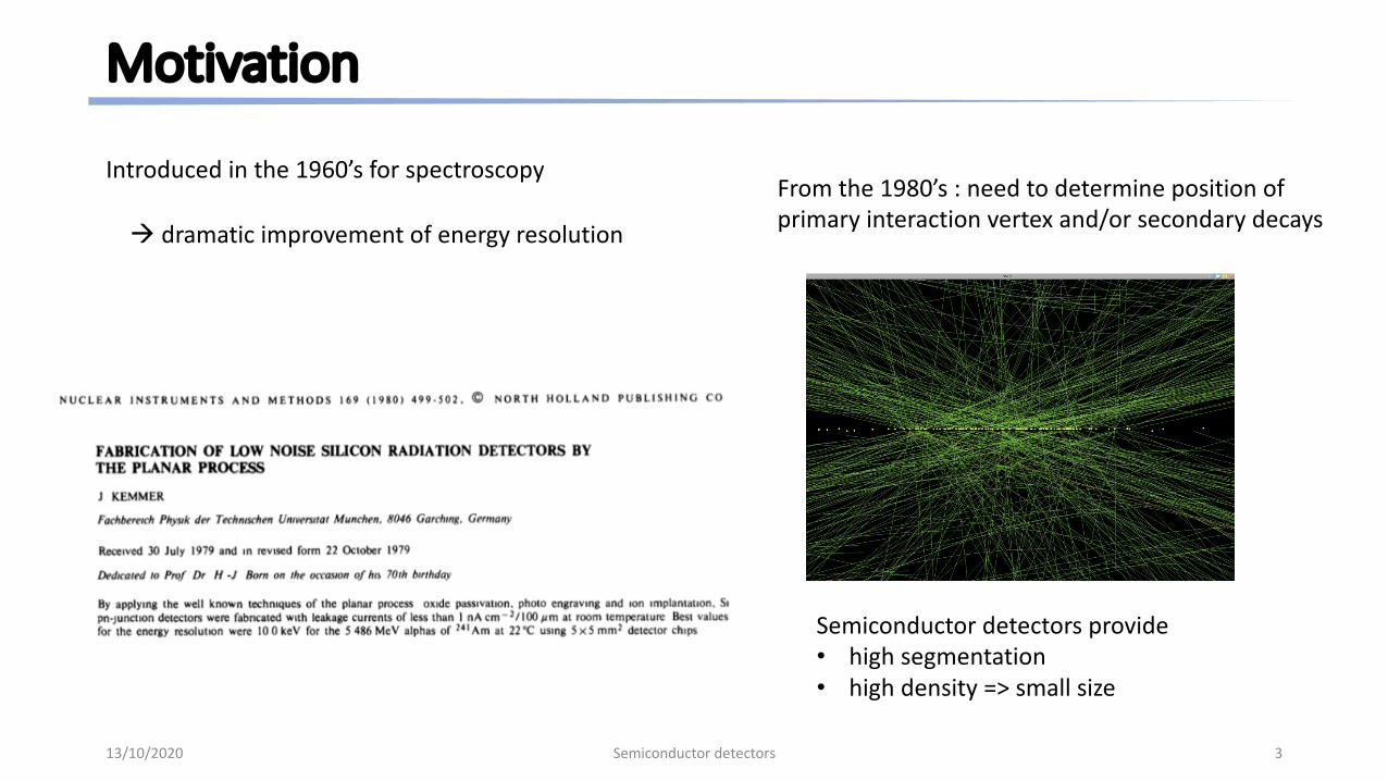
Dopedsemiconductors• Add impurities with different number of valence electrons
• Create additional levels in the bandgap, to be occupied by charge carriers
• Very small concentrations : 1012-1015 cm-3, vs 1020 cm-3 atoms of Si or Ge
13/10/2020 Semiconductordetectors 9
Donorimpurities(n-typedoping) :As,P,Sb5valenceelectrons
Acceptorimpurities(p-typedoping) :Ga,B,In3valenceelectrons
allthee- inexcessinthedonorlevelaretransferredtotheconductionbandbecauseofthermalenergy
theacceptorlevelisfilledwithe- fromthevalencebandbecauseofthermalenergy
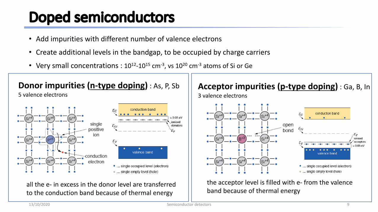
p-njunctionObtained by diffusing p-type impurities on one side of a n-type Si bar (”bulk”)
• (free) electrons migrate to the p side and fill the holes• (free) holes migrate to the n side and capture electrons
• creation of a depletion region with no charge carriers
• the n side is now charged +, the p side is charged - :
• creation of an electrical potential (built-in potential)
• this balances the chemical potential : equilibrium
13/10/2020 Semiconductordetectors 10

p-njunction:depletiondepthsuppose uniform charge density ρ(x) on both sides
charge conservation NAxp=NDxn
solve Poisson equation1=>13=
= −? 3@
using boundary conditions E(-xp)=E(xn)=0(Exercise1)
à ∆𝑉 = C'@
𝑁E𝑥F' + 𝑁H𝑥I'
à 𝑥F ='@∆>
CJK LMJK/JN
L/'𝑥I =
'@∆>CJN LMJN/JK
L/'
à 𝑑 = 𝑥F + 𝑥I ='@∆>C
JKMJNJKJN
L/'
13/10/2020 Semiconductordetectors 11
ρ(x)-xp
xn
ρ=eND
ρ=-eNA
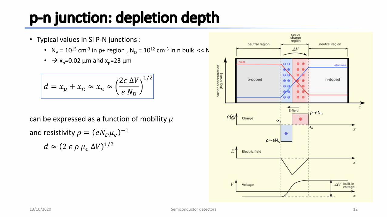
p-njunction:depletiondepth• Typical values in Si P-N junctions :
• NA = 1015 cm-3 in p+ region , ND = 1012 cm-3 in n bulk << NA
• à xp=0.02 μm and xp=23 μm
𝑑 = 𝑥F + 𝑥I ≈ 𝑥I ≈2𝜖∆𝑉𝑒𝑁H
L/'
can be expressed as a function of mobility μ
and resistivity 𝜌 = 𝑒𝑁H𝜇C TL
𝑑 ≈ 2𝜖𝜌𝜇C∆𝑉 L/'
13/10/2020 Semiconductordetectors 12
ρ(x)-xp
xn
ρ=eND
ρ=-eNA

Fromthep-njunctiontothedetector• The depth of the depletion region can be increased by applying an external voltage: reverse bias
ΔV -> ΔV+VB in the formula
(VB>>ΔV, so ΔV+VB~VB)
example : d=1mm VB=300V
The voltage V needed to deplete a device of thickness d is called the depletion voltage Vd
• The depleted region is the useful volume for detection
ionizing particles produce e--hole pairs
e- (holes) drift to the n (p) sideà current pulses
proportional to the energy deposit
13/10/2020 Semiconductordetectors 13

Semiconductordetectorcharacteristics• Charge collection
the drift velocity of electron/holes is ve = μe E, vh = μh E respectivelyThe mobility μ depends on T and E.
• Linearitythe depleted region has a capacitance C=εA/d
the observed voltage on the electrodes is then 𝑉 = UV= 𝑛 2
6Và linear with the deposited energy
• Energy resolution (Exercise 2)the intrinsic energy resolution depends on the number of carriers E/w and the Fano Factor F~0.12
𝑅 = 2.35𝐹𝑤𝐸
�
(+ contributions from other sources, e.g. electronics)
13/10/2020 Semiconductordetectors 14
A,d :detectorareaandthicknessn :collectionefficiencyE:electricfieldw:averageenergyfore-hpaircreation
ChargecollectionstimesO(10ns)à fast!

(parenthesis:theFano Factor)• Assume the formation of charge carriers to be a Poisson process:
• if 𝑁 carriers generated, the statistical fluctuation on that number is 𝑁�
• since 𝑁 is usually large, the detector response will follow a Gaussian distribution with mean = 𝑁 andstandard deviation = 𝑁�
• For a linear detector, where the response E is proportional to 𝑁, E=kN, the resolution is
𝑅 =𝐹𝑊𝐻𝑀𝐸 =
2.35𝜎 𝐸𝐸 =
2.35𝑘 𝑁�
𝑘𝑁 =2.35 𝑁�
𝑁• This is the intrinsic limit from statistical fluctuations. Better values are found from measurements in somedetectors.
• Processes leading to the formation of charge carriers are probably not completely independent: departurefrom Poisson statistics, quantified by the Fano Factor F
𝐹 =𝑜𝑏𝑠𝑒𝑟𝑣𝑒𝑑𝑣𝑎𝑟𝑖𝑎𝑛𝑐𝑒𝑜𝑛𝑁
𝑃𝑜𝑖𝑠𝑠𝑜𝑛𝑝𝑟𝑒𝑑𝑖𝑐𝑡𝑒𝑑𝑣𝑎𝑟𝑖𝑎𝑛𝑐𝑒(= 𝑁)
• so the resolution is 𝑅 = '.%lm J� n�
mJ= 2.35 n
J� = 2.35 n6
2�
13/10/2020 Semiconductordetectors 15
inscintillatorsF~1inSi/GeF~0.1

Semiconductordetectorcharacteristics
13/10/2020 Semiconductordetectors 16

Semiconductordetectorcharacteristics• Leakage current
Small fluctuating current flowing when VB is applied,although a reverse bias diode is ideally non-conducting.It limits the smallest signal pulse height that can beobserved.Several sources:• Generated current: thermally generated e-h pairs,separated by the electric field and collected at theends of the semiconductor volumeà reduced by using pure and defect-free
materials with high carriers lifetime, operateat low T
• Diffusion current: movement of minority chargecarriers
13/10/2020 Semiconductordetectors 17
M.Bomben,HDR

SomepropertiesofSiandGeasdetectorsSilicon(Si) Germanuim (Ge)
Z,A 14,28.1 32,72.6
ρ [g/cm2] 2.33 5.32
Eg (T=300K)[eV] 1.1 0.7
Eg (T=0K)[eV] 1.21 0.785
I0 (T=300K)[eV] 3.62 -
I0 (T=77K)[eV] 3.81 2.96
μe (T=300K)[cm2/Vs] 1350 3900
μh (T=300K)[cm2/Vs] 480 1900
13/10/2020 Semiconductordetectors 18
only~1/3ofdepositedenergygoesintoproductionofe-hpairs
• HighZ:goodforγ detection(σ forphotoelectriceffectx60Si)• Needscooling
• LowZ:goodforchargedparticles
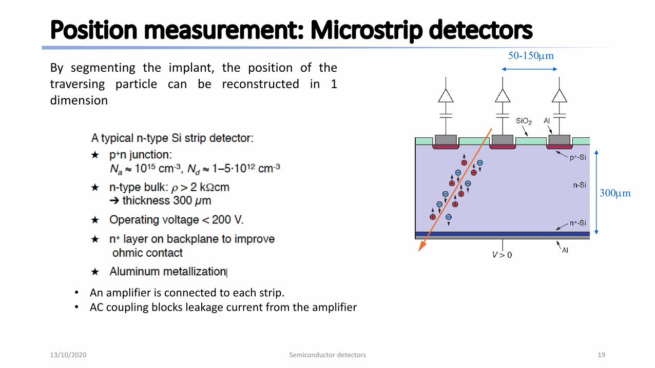
Positionmeasurement:Microstrip detectorsBy segmenting the implant, the position of thetraversing particle can be reconstructed in 1dimension
13/10/2020 Semiconductordetectors 19
300µm
50-150µm
• Anamplifierisconnectedtoeachstrip.• ACcouplingblocksleakagecurrentfromtheamplifier

Positionmeasurement:Microstrip detectorsBy segmenting the implant, the position of thetraversing particle can be reconstructed in 1dimension
àposition resolution = pitch/sqrt(12)~ O(10-50μm)
Diffusion:• caused by random motion during the drift
• width of charge cloud 𝜎H = 2𝐷𝑡� with 𝐷 = 𝑘𝑡𝜇/𝑒• typical 𝜎H = 8μm after 300μm drift
• can be used to improve position resolution (sharing ofsignal between adjacent strips)
13/10/2020 Semiconductordetectors 20
300µm
50-150µm
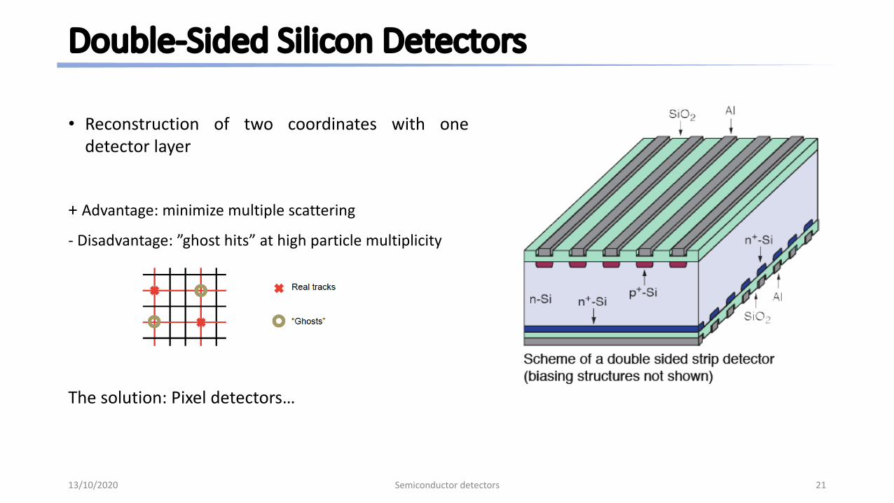
Double-SidedSiliconDetectors
• Reconstruction of two coordinates with onedetector layer
+ Advantage: minimize multiple scattering
- Disadvantage: ”ghost hits” at high particle multiplicity
The solution: Pixel detectors…
13/10/2020 Semiconductordetectors 21

PixelDetectors• Two-dimensional arrays of p-n diodes organised ina matrix
• Each p-n junction is readout by a dedicatedreadout integrated circuit
• Sensor and readout electronics are physicallyseparated and linked by a bump bonding
à Hybrid Pixel Detectors (HPDs)
+ Unambiguous 2D position measurement, pitch ~50μm
+ Smaller leakage currents than DSSD
- Large number of readout channels: complex solutions,large power consumption
13/10/2020 Semiconductordetectors 22

Examples
• To measure lifetimes of charmedmesons
• Surface: 24 cm2 (2” wafer) 1200 strip, 20μm pitch. Every 3rd/6th strip connected.Precision 4,5 μm !
• 8 Si detectors (2 in front, 6 behind theTarget)
13/10/2020 Semiconductordetectors 23
NA11atCERN,1983
Firstuse ofaposition-sensitiveSidetectorinHEP

Examples
13/10/2020 Semiconductordetectors 24
SiliconTrackerDetector(STD):9layersofdouble-sidedSisensors(2300)• Totalinstrumentedsurfacearea:6.45m2 with196kreadoutchannels
• Positionresolution:8.5µm(30µm)inthebending(non-bending)plane
• particlerigiditymeasurement(p/Z)of1.5%at10GeVandamaximumdetectablerigidityabove1TeV forprotons
• ChargeseparationofnucleiuptoZ=26(bydE/dxmeasurement)
AMS-02Large-acceptancespectrometerontheISS,since2011.Toperformprecisemeasurementsofchargedcosmicraysfluxesinawideenergyrange

Examples
13/10/2020 Semiconductordetectors 25
CMSThe4mainLHCexperiments(ATLAS,CMS,ALICE,LHCb)haveSitrackers
ATLASPixels:1744modules,80x106channels.Pixelsize50x400μm2 .Resolution14x115μm2
Strips:61m2 ofsilicon ,4088modules,6x106channelsReadout pitch80μm,hitresolution17μm
theworldlargest silicon tracker
~1m2 ofpixelsensors,60x106channels,hitresolution 10x17μm2
200m2 ofstrip sensors (singlesided)11x106readout channels,hitresolution 40-60μm

Examples
13/10/2020 Semiconductordetectors 26

Radiationdamage• Inelastic collisions of impinging particles on Si cause displacement of a Si atom from its lattice siteà point defects
• several defects grouped together can form a cluster the probability depends on the particle typeand energy. The amount increases with particle fluence.
àMacroscopic effects (”ageing”):
• increase of leakage current
• change in operation voltage
• reduction of signal amplitude
• à R&D for radiation-hard sensors
13/10/2020 Semiconductordetectors 27

SomeotherSidetectors
13/10/2020 Semiconductordetectors 28

Photodetectors:AvalanchePhotoDiodes (APD)
Conversion of photons into a charge current :e-h pair creation + avalanche multiplication
+ Gain O(100)+ Fast response times(formation of avalanche <ns)
- Large operation voltage (E > 105 V/cm)- Poor energy resolution (fluctuations in theavalanche), extremely sensitive to voltagechanges
13/10/2020 Semiconductordetectors 29
HamamatsuSiAPDS8890-10

Photodetectors:AvalanchePhotoDiodes (APD)
13/10/2020 Semiconductordetectors 30

Photodetectors:SiliconPhotoMultipliers (SiPM)Matrices of 100s-1000s APDs operated in Geiger mode
• The signal in each cell is not proportional to energy:on/off
• Count number of hit cellsàmeasure the photon flux
+ Gain ~105-107 (cfr PMTs)
+ Good charge resolution
+ No need for HV
+ Not sensitive to magnetic field
- Dark noise, crosstalk, afterpulses, …
13/10/2020 Semiconductordetectors 31
source:Hamamatsu

ExercisesExercise 1
Compute the solution to Poisson’s equation to obtain the depth of the depletion region (slide 11).
Exercise 2
Scintillators, gaseous and silicon detectors can be used to measure the energy lost by a particle. Thekey parameter is the energy necessary to create a scintillation photon (or a e/ion pair, or a e/holepair). Three cases are considered:
(i) Scintillator. 1 photon emitted for 100 eV deposited, 6% of photons reach the PMT, QE = 30%
(ii) Si detector. 3.6 eV are necessary to create a pair e/hole.
(iii) Gaseous detector. 20 eV necessary to create a pair e/ion.
What is the relative precision with which energy losses of (a) 100 keV, (b) 5 MeV, (c) 20 MeV can bemeasured in the three detectors? NB. We assume a Gauss statistics, the error on a count N issqrt(N).
13/10/2020 Semiconductordetectors 32