Embed Size (px)
Citation preview
Detectors for Wide Field Imaging
Gavin DaltonWith input from Paul Jorden, Peter Poole, Peter Dennis, David
Hall, David Lees, John Cairns, Keith Barnes, Ian Baker, Les
Hipwood, Gert Finger, Jim Beletic

Overview
• Current status of CCDs
• Current IR detectors
• Developments in IR detectors
• Prospects

CCDs
! Fairchild
! LBNL (Hamamatsu)
! e2V

CCDs! Fairchild
CCD486, 4kx4kx15µm
Better q.e. and slightly lower dark current than e2V CCD231
due to multi-phase pinning, but also higher readout noise
In recent discussions, Fairchild appeared to have no interest
in developing larger format CCDs

Fairchild q.e. curve
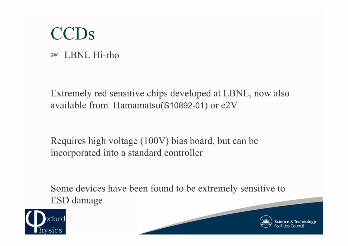
CCDs! LBNL Hi-rho
Extremely red sensitive chips developed at LBNL, now also
available from Hamamatsu(S10892-01) or e2V
Requires high voltage (100V) bias board, but can be
incorporated into a standard controller
Some devices have been found to be extremely sensitive to
ESD damage

CCDs! e2V
Stable production process based on building blocks
Blue, Red and High-rho devices available
Anti-fringing options (variable pixel heights)
Provides a simplified controller interface
Avalanche gain, not yet mapped to larger formats
Formats up to 8kx3k have been manufactured (larger than
4kx4k is probably lower cost for large systems)
Also making 10µm pixel high-rho devices for LSST
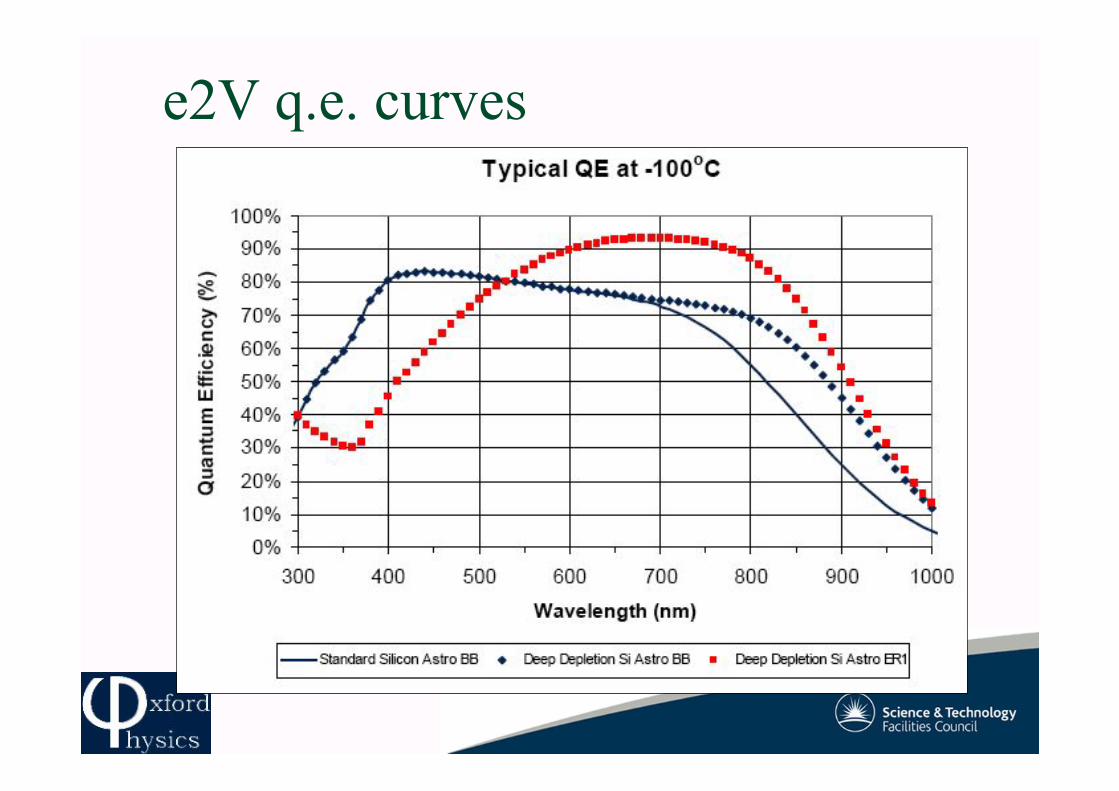
e2V q.e. curves

e2V q.e. curves

e2V package
CCD231-84 package
15µm pixels
2e- noise at 50kHz readout
5e- noise at 1MHz readout
SiC package provides 20µm
flatness

Current IR arrays! Raytheon
" 2kx2kx20µm VIRGO chips (VISTA)
" 2.5µm cut-off, good q.e, poor cosmetics
• Low cost option, mixed experience from VISTA
• 3-edge-buttable
! Teledyne" 2kx2kx18µm HAWAII-2RG
" 2.5 or 1.7µm cut-off, substrate removed
" 3-edge buttable
" Highly functional ROIC with option for multiple fastreadout windows to prevent saturation and persistence
" SIDECAR integrated ASIC controller

Array Fabrication Technology
!HgCdTe layer grown on
ZnCdTe substrates (good
lattice match) using MBE
(RVS still using LPE)
!Detector layer hybridised
to Si CMOS ROIC
! Limitations on array size,
performance and
yield/lifetime (-> cost)

Teledyne developments!Developing 2kx2kx30µm array
as precursor to 4kx4kx15µmHAWAII-4RG

Performance Issues
!Channel cross-talk (from ESO’s X-Shooter,courtesy G. Finger)

Performance Issues
!Fringing due to substrate…

Performance Issues!Persistence…
74
7170
32252
1.24 108 photons/s/pixel
Flux of bright source before
taking dark exposures
0 500 Time (s) 1500 2000
Re
mn
an
t S
ign
al (e
- )
100
50
0
Remnant
image of
bright
source in
preceding
exposure
sometimes
visible for
hours after
event.

Performance Issues! Inter-pixel capacitance
" Leads to over-estimation of system gain, and hence quantumefficiency
! Photo-emission defects
" Occasionally individual pixels seen to act as bright IR LEDs
! Catastrophic failures…
" A large number of early arrays have now been observed todelaminate after repeated cold cycling

New developments in IR
!ESA TRP for Cosmic Visions
" Promote development of EU competitor to
Teledyne for next generation space missions
!SELEX-Galileo
!QinetiQ

OSPREY 384 x 288
24!m pitch MW and LW
EAGLE 640 x 512
24!m pitch MW and LW
HAWK 640 X 512
16!m pitch MW and LW
Dry etched mesas
MERLIN 1024 x 768
16!m pitch MW and LW
Dry etched mesas
CONDOR 640 x 512
24!m pitch Two Colour
Dry etched mesas
Larger area
Smaller pixels
Multicolour detectors
by Merlin MWIR
Evolution of 2D arrays at SELEX

SELEX Capabilities!HgCdTe grown by MOVPE on GaAs substrates then hybridised
!GaAs 100x less expensive than lattice matched CdZnTe
!Multiple suppliers (CZT has limited no. of commercial suppliers)
!Wafer scale (150mm) processing using standard semiconductor equipment
!Few mask stages
!New bump bonder being installed. 150mm array end-end capability
!Should be able to produce low-cost equivalent of HAWAII-2RG devices
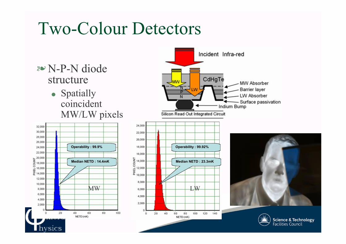
Two-Colour Detectors
!N-P-N diodestructure" Spatially
coincidentMW/LW pixels
Median NETD : 14.4mK
Operability : 99.9%
Median NETD : 23.3mK
Operability : 99.92%
MW LW

HgCdTe as IR detector invented at
Malvern in 1959
128 x 128 HgCdTe hybridised on Si
55!m pitch LW (10!m)
1024 x 768 HgCdTe hybridised on Si
26!m pitch LW (9.6!m)
Dual band arrays
30!m pitch MW and LW
two capacitors/pixel
Evolution of 2D arrays at QinetiQ

Developments - QinetiQ
! MOVPE growth at high T gives much more control of growthenvironment than MBE process
! Direct growth onto ROIC mesas - no substrate
! Si substrates ultimately available up to 300mm
! Key technology is the survivability of the ROIC structure inthe MOVPE growth environment

MCT Island Growth on ROICSOptical micrograph showing ROIC pixels
Crystalline Si surface
growth window
Integrated circuits surrounding
growth window

MCT Island Growth on ROICS
Crystalline
MCT in
window areas
Polycrystalline
MCT
•Scanning electron micrograph

Crystalline
MCT mesas
Silicon circuit
•Scanning electron micrograph of part of processed FPA
MCT Island Growth on ROICS
Contact
pads

MCT Island Growth on ROICS•Example of prototype FPA
Mesa contact
Passivation
Etched mesa
Mesa contact

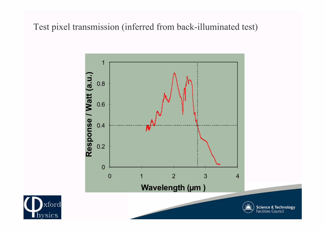
Test Pixel Growth
p-type contact
(bottom)
n-type contact
(top)
75µm pixel grown in 100µm
growth window on a test
wafer
0
0.2
0.4
0.6
0.8
1
0 1 2 3 4
Wavelength (!m )
Re
sp
on
se
/ W
att
(a
.u.)
Test pixel transmission (inferred from back-illuminated test)

Developments - QinetiQ
! MOVPE growth at high T gives much more control of growth environment thanMBE process
! Direct growth onto ROIC mesas - no substrate
! Si substrates ultimately available up to 300mm
! Key technology is the survivability of the ROIC structure in the MOVPE growthenvironment
! Good SW (1-2.5µm) material performance demonstrated
! Larger (36µm) pixels optimal for some ELT instruments
" NB for 150mm wafers and 50µm pixels = 2048x2048 array (c.f. end of VISTA talk)
• Key specifications appropriate to ELT instruments can be met - Good q.e. &linearity
• Not able to measure dark current at astronomical level
• Key aims are to demonstrate modest array-scale growth of SW device on anappropriate ROIC

Small pitch IIDC
!XH035 0.35µm Alprocess
!Growth area~12.25µm x 11.5µm
!Fill factor ~30%
! CX06XI10 0.6µm W process
! Pixel growth area ~18.5µm x
18.4µm
! Fill factor ~ 38%
30µm
30µm
20µm
20µm

Optical concentrators –
immersion lens
!One immersion lens / 4 pixels

Constant pitch ROIC
!CX06XI10 0.6µm W process
!Pixel growth area ~13µm x 13µm
!Fill factor ~ 19%
30µm
30µm

Optical concentrators - cones
! Low gain option with area gain of 4
! Substantially reduces dark current/”pixel”
30!m
15!m
Infrared from
objective lens
15!m

Prospects
!ESA TRP announced last week for NIRdetector development
" Terms look favourable to both SELEX andQinetiQ development routes
!SELEX probably provides the best route toa quick replacement for a H-2RG/H-4RGtype device…
!QinetiQ probably more interesting for wide-field imaging considerations: possibility ofmigrating to 12” silicon wafer scale devices.

Longer term…?