Embed Size (px)
Citation preview

ISSN 1063�7842, Technical Physics, 2015, Vol. 60, No. 7, pp. 1044–1050. © Pleiades Publishing, Ltd., 2015.Original Russian Text © O.A. Ageev, O.I. Il’in, M.V. Rubashkina, V.A. Smirnov, A.A. Fedotov, O.G. Tsukanova, 2015, published in Zhurnal Tekhnicheskoi Fiziki, 2015, Vol. 85, No. 7,pp. 100–106.
1044
INTRODUCTION
Owing to a unique combination of electrical,mechanical, and geometric properties, verticallyaligned carbon nanotubes (VA CNTs) are widely usedto create promising nanoelectronic devices, such asfield�emission emitters, transistors, memory ele�ments, and interconnections [1–3]. As a rule, themain properties of VA CNTs that determine theparameters of such devices are electrical resistivity andresistance per unit length. It is difficult to determinethese VA CNTs parameters by standard methodsbecause of the vertical orientation of nanotubes andtheir high aspect ratio. For example, the two� andfour�probe methods that are widely used to study theelectrical properties of microstructures need contactpads several microns in size at the top of a VA CNTarray, which significantly limits the possibilities ofapplication of these methods to determine the electri�cal parameters of individual vertically aligned nano�tubes because of their small sizes [4]. The problemsrelated to the development of new techniques of nan�odiagnostics to determine the electrical parameters ofvertically aligned nanotubes become challenging dueto the necessity of controlling and studying the electri�cal parameters of individual VA CNTs and construc�tion and device elements based on them and due to therequirements of developing the metrology of nano�technologies.
Scanning probe microscopy (SPM), which can beused to measure the I–V characteristics of nanotubes,
is a precision method for studying the electrical prop�erties of individual carbon nanotubes (CNTs) [5, 6].This method does not require additional fixation ofVA CNTs and the formation of contact pads at theirtop. However, when VA CNTs are studied by SPM,difficulties related to the mobility of nanotubes duringcontact with a probe and the formation of VA CNTbundles in an applied electric field arise [6]. Moreover,the determination of the electrical resistivity of CNTsfrom the I–V characteristics obtained by SPMrequires an analysis of the measurement of I–V char�acteristic and the related development of a techniqueto find the electrical parameters of VA CNTs withallowance for the specific features of SPM.
The purpose of this work is to develop an SPMtechnique to determine the electrical resistivity andthe resistance per unit length of VA CNTs.
EXPERIMENTAL
A sample with a VA CNT array was grown byplasma�enhanced chemical vapor deposition in amultifunctional NANOFAB NTK�9 (NT�MDT, Rus�sia) nanotechnology facility. VA CNTs were grown on asilicon wafer containing catalytic nickel centers on itssurface. A 20�nm�thick titanium film was used as a lowerconducting and adhesion layer on the silicon wafer.
The geometric parameters of the VA CNT arraywere studied by a Nova NanoLab 600 (FEI, the Neth�erlands) scanning electron microscope (SEM). TheVA CNT diameter and height were 98 nm and 2.2 μm,
Determination of the Electrical Resistivity of Vertically Aligned Carbon Nanotubes by Scanning Probe Microscopy
O. A. Ageev*, O. I. Il’in, M. V. Rubashkina, V. A. Smirnov, A. A. Fedotov, and O. G. Tsukanova
Southern Federal University, Institute of Nanotechnologies, Electronics, and Equipment Engineering,Nekrasovskii per. 44, Taganrog, 347900 Russia
*e�mail: [email protected] September 1, 2014
Abstract—Techniques are developed to determine the resistance per unit length and the electrical resistivityof vertically aligned carbon nanotubes (VA CNTs) using atomic force microscopy (AFM) and scanning tun�neling microscopy (STM). These techniques are used to study the resistance of VA CNTs. The resistance ofan individual VA CNT calculated with the AFM�based technique is shown to be higher than the resistance ofVA CNTs determined by the STM�based technique by a factor of 200, which is related to the influence of theresistance of the contact of an AFM probe to VA CNTs. The resistance per unit length and the electrical resis�tivity of an individual VA CNT 118 ± 39 nm in diameter and 2.23 ± 0.37 μm in height that are determined bythe STM�based technique are 19.28 ± 3.08 kΩ/μm and 8.32 ± 3.18 × 10⁻⁴ Ω m, respectively. The STM�basedtechnique developed to determine the resistance per unit length and the electrical resistivity of VA CNTs can beused to diagnose the electrical parameters of VA CNTs and to create VA CNT�based nanoelectronic elements.
DOI: 10.1134/S1063784215070026
PHYSICS OF NANOSTRUCTURES

TECHNICAL PHYSICS Vol. 60 No. 7 2015
DETERMINATION OF THE ELECTRICAL RESISTIVITY 1045
respectively, and the nanotube density in the array was8 μm–2 (Fig. 1).
The electrical properties of VA CNTs were studiedby an Ntegra (NT�MDT, Russia) scanning probe lab�oratory by contact atomic force microscopy (AFM) inthe current spectroscopy mode and by scanning tun�neling microscopy (STM) in the STM spectroscopymode at a distance of 0.5 nm between an STM probeand VA CNTs. As the AFM probe, we used a commer�cial cantilever with an NSG11/Pt platinum coating.As the STM probe, we used a tungsten probe 52 nm inradius, which was sharpened by an electrochemicalmethod [7]. To localize a probe at the top of VA CNTs,we performed preliminary scanning of the array sur�face using AFM in the tapping mode and using STMin the dc mode. The AFM and STM images of theVA CNT array are shown in Figs. 2a and 3a, respec�tively. The VA CNT diameter was determined by pro�cessing the AFM and STM images using the ImageAnalysis (NT�MDT, Russia) software package(Figs. 2b, 3b). During statistical processing of theSTM image by the Grain Analysis function, a cutplane was drawn parallel to the vertices of VA CNTs inorder to determine the cross�sectional area and thediameter of each nanotube cut by this plane (Fig. 3b).
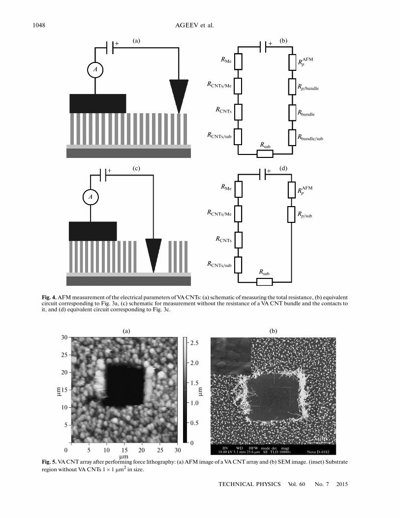
The I–V characteristics of VA CNTs obtained byAFM and STM spectroscopy are shown in Figs. 2cand 3c (solid lines), respectively. The scheme of mea�suring the I–V characteristic of VA CNTs by contactAFM is shown in Fig. 4a, and the scheme of STMmeasurement is similar with allowance for the fact thattunneling contact is formed between an STM probeand VA CNTs.
The resistance of the probe/conducting layer/VACNT array/contact system was additionally measuredusing the circuit presented in Fig. 4c to exclude theresistances of the probe material, the conducting layer,the contact, and the array of the nanotubes under itfrom the total resistance of the probe/VA CNT/con�ducting layer/VA CNT array/contact system. To mea�sure this resistance, we preliminarily performed forcelithography of the VA CNT array by AFM using thetechnique from [8]. Figure 5 shows AFM and SEMimages of the modified region in the sample. Whenanalyzing the AFM image by the technique describedin [8], we were able to find the average VA CNT height(2.23 ± 0.37 μm), which correlates with the results ofanalysis of the SEM image (Fig. 1). Figures 2c and 3cshow the I–V characteristics of the modified regionobtained by AFM and STM spectroscopy (dottedlines), respectively.
RESULTS AND DISCUSSION
An analysis of the AFM image of the VA CNT arraytaken in the tapping mode demonstrates that individ�ual nanotubes are joined into bundles 320–650 nm indiameter during mechanical interaction with theAFM probe, which hinders the investigation of the
electrical properties of individual nanotubes (Fig. 2a).The mechanism of formation of VA CNT bundles andthe techniques of determining their geometric param�eters when a VA CNT array is studied by AFM in thetapping mode were described in [8]. Figure 2c (solidline) shows the I–V characteristic of a bundle ofVA CNTs 612 nm in diameter consisting of eight indi�vidual nanotubes. The VA CNT bundle has the follow�ing two states of conduction: a high�resistance statewhen the voltage changes from 0 to 10 V and a low�resistance state when the voltage changes from 10 to0 V, which is associated with the resistance propertiesof VA CNTs [9]. To determine the resistance ofVA CNTs, we used the I–V characteristic that corre�sponds to the low�resistance state of the VA CNT bundle,since no additional resistance related to the internal fieldin nanotubes appears in VA CNTs in this case [9].
An analysis of the measurement of the I–V charac�teristic of the VA CNT bundle showed that the AFMprobe/VA CNT/conducting layer/VA CNTarray/contact system can be represented by the equiv�alent circuit shown in Fig. 4b. The total resistance of
this system is
(1)
(2)
where is the total resistance of the conductinglayer (Rsub), the contact material (RMe), the AFM
probe material ( ), the nanotube array under thecontact and the contacts to it (RCNTs/Me + RCNTs +
RtotAFM
RtotAFM R0
AFM Rbundle/sub Rbundle Rp/bundle,+ + +=
R0AFM RMe RCNTs/Me RCNTs RCNTs/sub+ + +=
+ Rsub RpAFM
,+
R0AFM
RpAFM
3 µm1 µm mode
SEdet
CDEMmag
25000× Nova D�0182
Fig. 1. SEM image of a VA CNT array: (inset) top view.

1046
TECHNICAL PHYSICS Vol. 60 No. 7 2015
AGEEV et al.
RCNTs/sub); Rbundle/sub + Rbundle + Rp/bundle is the resis�tance of the VA CNT bundle and the contacts to it.
Resistances and are determined by ananalysis of the linear segments of the I–V characteris�tics obtained by AFM spectroscopy on the VA CNTbundle and on the VA CNT array region modified byforce lithography (Fig. 2c). An analysis of the mea�surement of the I–V characteristic of the modifiedregion in the VA CNT array showed that the AFMprobe/conducting layer/VA CNT array/contact sys�tem can be represented by the equivalent circuit repre�
sented in Fig. 4d. Resistance is found to be452 MΩ on the assumption that the resistance of thecontact of the AFM probe with the metallic film of theconducting layer meets the relations Rp/sub � Rp/bundle,Rp/sub � Rbundle, and Rp/sub � Rbundle/sub. Resistance
RtotAFM R0
AFM
R0AFM
for the low�resistance state of the VA CNT bun�dle is 533 MΩ (Fig. 2c). Therefore, the resistance ofthe VA CNT bundle and the contacts to it is
(3)
Since VA CNTs are joined into bundles during anAFM investigation (Fig. 2a), the resistance of one nano�
tube and the contacts to it ( ) can be written as
(4)
where N is the number of nanotubes in the VA CNT
bundle. According to Eq. (4), resistance is10.1 MΩ. This VA CNT resistance is overestimated,since it includes both the VA CNT resistance and the
RtotAFM
Rbundle/sub Rbundle Rp/bundle+ + RtotAFM R0
AFM.–=
RCNTAFM
RCNTAFM Rtot
AFM R0AFM–
N�������������������������,=
RCNTAFM
5
4
3
2
1
0 1 2 3 4 5
1.5
1.0
0.5
0
μm
µm
µm
(a)
0.5
0.4
0.3
0.2
0.1
0 0.2 0.4 0.6 0.8 1.0Plane, μm
µm
(b)
16
14
12
10
8
6
4
2
00 1 2 3 4 5 6 7
U, V
I, n
A
SubstrateVA CNT
(с)
Fig. 2. AFM study of a VA CNT array: (a) AFM image of a VA CNT array, (b) profilogram along a line, and (c) I–V characteristicsof (solid line) nanotube bundle and (dotted line) substrate.

TECHNICAL PHYSICS Vol. 60 No. 7 2015
DETERMINATION OF THE ELECTRICAL RESISTIVITY 1047
resistance of the contact of the AFM probe to the topof the VA CNT bundle (Rp/bundle) and the contact to theconducting layer (Rbundle/sub). As was shown in [10], theresistance of the contact of an AFM probe with a plat�inum coating to the top of VA CNTs can reach severalhundreds kiloohms. It should also be noted that theresistance of a VA CNT bundle differs from the sum ofthe resistances of its individual nanotubes because ofthe van der Waals interaction between CNTs [11].Moreover, nanotubes in a bundle differ from eachother in the geometric parameters, which also affectsthe resistance of VA CNTs determined by AFM spec�troscopy.
To exclude the resistance of the contact of theprobe with the top of a VA CNT bundle (Rp/bundle), weperformed similar measurements of the I–V charac�teristic of VA CNTs by STM spectroscopy (Fig. 3). Ananalysis of the obtained STM image of a VA CNT arrayshowed that (Fig. 3b), in contrast to the results shownin Fig. 2a, the individual nanotubes are not joined into
VA CNT bundles because of a low CNT density in anarray and the VA CNT diameter is 118 ± 39 nm, whichmakes it possible to study the electrical properties ofindividual VA CNTs. Based on the I–V characteristicof an individual VA CNT (Fig. 3c), we can concludethat an individual VA CNT also has two states of con�duction and that the I–V characteristic that corre�sponds to the low�resistance state of VA CNT shouldbe used to determine the VA CNT resistance [9].
An analysis of the measurement of the I–V charac�teristic of an individual VA CNT by STM showed thatthe measurement system can be represented by theequivalent circuit represented in Fig. 6a. The total
resistance of the system ( ) is
(5)
(6)
RtotSTM
RtotSTM R0
STM RCNT/sub RCNT Rtun,+ + +=
R0STM RMe RCNTs/Me RCNTs RCNTs/sub+ + +=
+ Rsub RpSTM
,+
350
43
21
01
23
4µm
nm
1 2 3 40
30
25
20
15
5
4
3
2
1
0μm
µm
µm
nm
5
4
3
2
1
0 1 2 3 4 5μm
µm
12 3
45
(a) (b)
10–5
10–6
10–7
10–8
10–9
0 0.5 1.0 1.5 2.0 2.5 3.0U, V
I, A
SubstrateVA CNT
(c)
Fig. 3. STM study of a VA CNT array: (a) STM image of a VA CNT array, (b) profilogram along a line, and (c) I–V characteristicsof (solid line) an individual nanotube at point 3 and (dotted line) substrate.
1048
TECHNICAL PHYSICS Vol. 60 No. 7 2015
AGEEV et al.
(a) (b)
RMe
RCNTs/Me
RCNTs
RCNTs/sub
A
A
(c)
RMe
RCNTs/Me
RCNTs
RCNTs/sub
Rsub
Rp
Rp/sub
AFM
Rsub
RpAFM
Rp/bundle
Rbundle
Rbundle/sub
(d)
Fig. 4. AFM measurement of the electrical parameters of VA CNTs: (a) schematic of measuring the total resistance, (b) equivalentcircuit corresponding to Fig. 3a, (c) schematic for measurement without the resistance of a VA CNT bundle and the contacts toit, and (d) equivalent circuit corresponding to Fig. 3c.
5 µm
HV10.00 kV
WD5.1 mm
HFW25.6 µm
modeSE
detTLD
magt10000× Nova D�0182
30
25
20
15
10
5
0 5 10 15 20 25 30
2.5
2.0
1.5
1.0
0.5
0
μm
µm
µm
(a) (b)
Fig. 5. VA CNT array after performing force lithography: (a) AFM image of a VA CNT array and (b) SEM image. (inset) Substrateregion without VA CNTs 1 × 1 µm2 in size.
TECHNICAL PHYSICS Vol. 60 No. 7 2015
DETERMINATION OF THE ELECTRICAL RESISTIVITY 1049
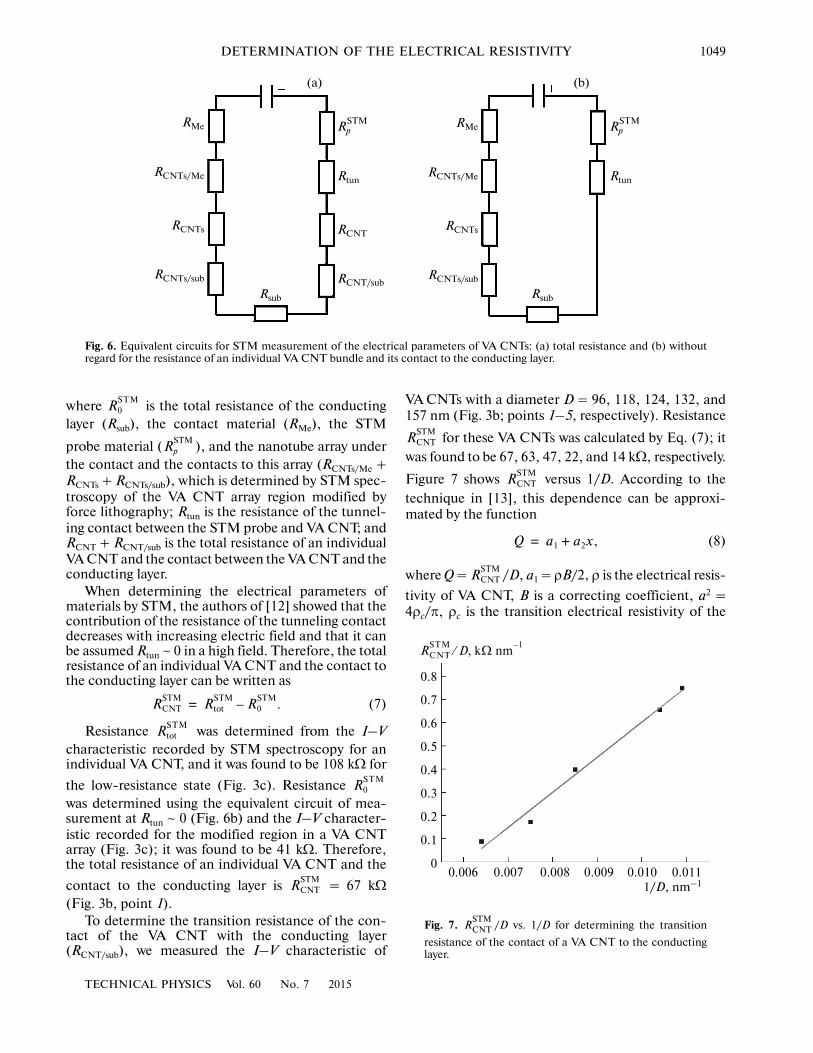
where is the total resistance of the conductinglayer (Rsub), the contact material (RMe), the STM
probe material ( ), and the nanotube array underthe contact and the contacts to this array (RCNTs/Me +RCNTs + RCNTs/sub), which is determined by STM spec�troscopy of the VA CNT array region modified byforce lithography; Rtun is the resistance of the tunnel�ing contact between the STM probe and VA CNT; andRCNT + RCNT/sub is the total resistance of an individualVA CNT and the contact between the VA CNT and theconducting layer.
When determining the electrical parameters ofmaterials by STM, the authors of [12] showed that thecontribution of the resistance of the tunneling contactdecreases with increasing electric field and that it canbe assumed Rtun ~ 0 in a high field. Therefore, the totalresistance of an individual VA CNT and the contact tothe conducting layer can be written as
(7)
Resistance was determined from the I–Vcharacteristic recorded by STM spectroscopy for anindividual VA CNT, and it was found to be 108 kΩ for
the low�resistance state (Fig. 3c). Resistance was determined using the equivalent circuit of mea�surement at Rtun ~ 0 (Fig. 6b) and the I–V character�istic recorded for the modified region in a VA CNTarray (Fig. 3c); it was found to be 41 kΩ. Therefore,the total resistance of an individual VA CNT and the
contact to the conducting layer is = 67 kΩ(Fig. 3b, point 1).
To determine the transition resistance of the con�tact of the VA CNT with the conducting layer(RCNT/sub), we measured the I–V characteristic of
R0STM
RpSTM
RCNTSTM Rtot
STM R0STM
.–=
RtotSTM
R0STM
RCNTSTM
VA CNTs with a diameter D = 96, 118, 124, 132, and157 nm (Fig. 3b; points 1–5, respectively). Resistance
for these VA CNTs was calculated by Eq. (7); itwas found to be 67, 63, 47, 22, and 14 kΩ, respectively.
Figure 7 shows versus 1/D. According to thetechnique in [13], this dependence can be approxi�mated by the function
(8)
where Q = /D, a1 = ρB/2, ρ is the electrical resis�
tivity of VA CNT, B is a correcting coefficient, a2 =4ρc/π, ρc is the transition electrical resistivity of the
RCNTSTM
RCNTSTM
Q a1 a2x,+=
RCNTSTM
RMe
RCNTs/Me
RCNTs
RCNTs/sub
Rp
Rtun
RCNT
RCNT/sub
STM Rp
Rtun
STMRMe
RCNTs/Me
RCNTs
RCNTs/sub
Rsub Rsub
(a) (b)
Fig. 6. Equivalent circuits for STM measurement of the electrical parameters of VA CNTs: (a) total resistance and (b) withoutregard for the resistance of an individual VA CNT bundle and its contact to the conducting layer.
0.8
0.7
0.6
0.5
0.4
0.3
0.2
0.1
00.006 0.007 0.008 0.009 0.010 0.011
1/D, nm–1
RCNTSTM
D kΩ,⁄ nm1–
Fig. 7. /D vs. 1/D for determining the transition
resistance of the contact of a VA CNT to the conductinglayer.
RCNTSTM
1050
TECHNICAL PHYSICS Vol. 60 No. 7 2015
AGEEV et al.
contact of the VA CNT with the conducting layer,and x = 1/D.
An analysis of the dependence of /D on 1/D(Fig. 7) using the technique from [13] showed thatρc = 118.6 kΩ nm2 (1.186 × 10⁻⁹ Ω cm2). Therefore,the resistance of the contact for the VA CNTs understudy changes in the range RCNT/sub = 4.1–12.8 Ω.
Thus, we have RCNT/sub � and this resistanceweakly contributes to the resistance of VA CNTs deter�mined by the STM technique.
With allowance for the geometric parameters ofVA CNTs, resistance per unit length r and electricalresistivity ρ of VA CNTs are 19.28 ± 3.08 kΩ/μm and8.32 ± 3.18 × 10⁻⁴ Ω m, respectively. These values ofresistance per unit length and electrical resistivity ofmultilayer VA CNTs agree well with the data in [14, 15].
CONCLUSIONS
The electrical properties of VA CNTs were studiedby AFM and STM. Based on the obtained results andusing force lithography, we developed techniques todetermine the resistance per unit length and the elec�trical resistivity of an individual VA CNT. When theresistance of a VA CNT was determined by AFM, theresistance per unit length and the electrical resistivityof VA CNTs were shown to be higher than thoseknown from the literature, which is likely to be relatedto the effect of the contact of an AFM probe to the topof VA CNTs and the appearance of an additional resis�tance in the measuring system. Moreover, it was shownthat VA CNT bundles form when preliminary scan�ning is performed by AFM in the tapping mode inorder to position the AFM probe at the top ofVA CNTs. These bundles hinder the investigation ofthe electrical properties of an individual nanotube.
When determining the resistance of an individualVA CNT by STM, we were able to overcome these dif�ficulties, since the resistance of the tunneling contact ofan STM probe with the top of VA CNTsbecomes insignificant at a voltage higher than 1 Vand weakly affects the total resistance of the STMprobe/VA CNT/conducting layer/VA CNT array/con�tact system. Moreover, VA CNT bundles do not formduring preliminary STM scanning of the surface of theVA CNT array under study. It was shown that the tran�sition electrical resistivity of the contact of an individualVA CNT to the conducting layer is 1.186 × 10⁻⁹ Ω cm2 andcan be omitted in determining the resistance ofVA CNTs. The values of the resistance per unit lengthand the electrical resistivity of VA CNTs calculated bythe developed STM technique were found to be 19.28 ±3.08 kΩ/μm and 8.32 ± 3.18 × 10⁻⁴ Ω m, respectively,which agree well with the reported data.
Thus, the developed STM technique of determin�ing the resistance per unit length and the electricalresistivity of VA CNTs can be used to find the electrical
RCNTSTM
RCNTSTM
parameters of an individual VA CNT without addi�tional fixation of a nanotube and preliminary forma�tion of contact pads to it. In addition, it can be appliedto diagnose the electrical parameters of VA CNTs andto create nanoelectronic elements based on them.
ACKNOWLEDGMENTS
The experimental results were obtained on theequipment of the Center of Collective Use and theScientific�Education Center Nanotechnologies ofSouthern Federal University.
This work was supported by the Ministry of Scienceand Education of the Russian Federation (projectnos. 1936, 16.1154.2014/K), project 14.575.21.0045(unique identifier RFMEFI57514X0045), and theRussian Foundation for Basic Research (projectnos. 14�07�31322mol_a, 14�07�31162mol_a).
REFERENCES
1. Y. Lan, Y. Wang, and Z. Ren, Adv. Phys. 60, 553 (2011).2. X. V. Lu and J. Y. Dai, Appl. Phys. Lett. 88, 113104
(2006).3. H. Li and K. Banerjee, IEEE Trans. Electron Devices
56, 2202 (2009).4. N. Chiodarelli, S. Masahito, Y. Kashiwagi, Y. Li,
K. Arstila, O. Richard, D. J. Cott, M. Heyns, St. Gendt,G. Groeseneken, and Ph. M. Vereecken, Nanotechnol�ogy 22, 085302 (2011).
5. K. Ichimura, M. Osawa, K. Nomura, H. Kataura,Y. Maniwa, S. Suzik, and Y. Achiba, Physica B 323, 230(2002).
6. O. A. Ageev, Yu. F. Blinov, O. I. Il’in, A. S. Kolomiitsev,B. G. Konoplev, M. V. Rubashkina, V. A. Smirnov, andA. A. Fedotov, Tech. Phys. 58, 1831 (2013).
7. B. G. Konoplev, O. A. Ageev, A. S. Kolomiitsev,V. A. Smirnov, and N. I. Serbu, Mikroelektronika 41,47 (2012).
8. O. A. Ageev, O. I. Il’in, A. S. Kolomiitsev, B. G. Kono�plev, M. V. Rubashkina, V. A. Smirnov, andA. A. Fedotov, Mikro�Nanosist. Tekh., No. 3, 9 (2012).
9. O. A. Ageev, Yu. F. Blinov, O. I. Il’in, M. V. Rubashkina,V. A. Smirnov, and A. A. Fedotov, in Proceedings of theInternational Symposium “Physics and Mechanics ofNew Materials and Underwater Applications,” Thailand,2014, p. 12.
10. Q. Ngo, D. Petranovic, Sh. Krishnan, A. M. Cassell,Q. Ye, J. Li, M. Meyyappan, and C. Y. Yang, IEEETrans. Nanotechnol. 3, 311 (2004).
11. G. Kim, J. Bernholc, and Y.�K. Kwon, Appl. Phys.Lett. 97, 063113 (2010).
12. H. Won and R. F. Willis, Surf. Sci. 604, 491 (2010).13. Yu. D. Chistyakov, V. V. Baranov, and A. P. Dostanko,
Obz. Electron. Tekh., Ser. Poluprovod. Prib., No. 7(143), 364 (1973).
14. B. Vivo, P. Lamberti, G. Spinelli, and V. Tucci, Rom. J.Inf. Sci. Tech. 13, 33 (2010).
15. D. Fathi and B. Forouzandeh, Carbon Nanotubes,Ed. by J. M. Marulanda (InTech., 2010), pp. 275–297.
Translated by K. Shakhlevich


![RESISTIVITY [ ]](https://img.pdfslide.net/doc/110x75/6249524a7a9f6a12787a8128/resistivity-.jpg)

