Embed Size (px)
Citation preview

Elma electronic Inc. 44350 Grimmer Blvd
Fremont, CA. 34538 VPX White Paper Series Phone: 510 656 3400 VPX‐3U‐101511
www.elma.com Fax: 510 656 3783 www.elmasystems.com
Page 1 of 13
Developing FPGA Based Systems with VPX When developing applications with FPGAs using VITA 65 OpenVPX, a base interconnect architecture is necessary. A general system architecture that supports compute intensive pipelined applications can be characterized by a Front‐End Processing Cluster, and a Back‐End Processing Cluster as depicted in Figure One.
The Front‐End Cluster is responsible for initial data acquisition and preprocessing of the raw input data. Often system application data flows will involve multiple data streams that are assigned to different FGPA resources. For instance in a Radar application, the Radar Array Antenna may divide into regions which can be associated with a sensor area to be processed by a specific FPGA resource. The FPGAs can be organized to form a processor pipeline as shown in Figure 3. The Front‐End Cluster as shown, is composed on “N” FGPA resources, and a Control Processor. The data paths in and out of the FPGAs are implemented using serial interconnects, routed over a VPX Backplane. In the Front‐End Cluster a control processor is associated with the FPGA elements. The Control Processor can be used to manage the FGPA cards, and provides a multi‐core processor resource. The Control Processor is connected via a PCIe Switch to other system elements. A switch is used to connect the SBC to the FGPAs.
Once data is received and processed by the Front‐End Cluster, it can be passed down to another resource for further processing. Post processing involves final computations and processes, or potentially a display process. The Back‐End Cluster is comprised of a Graphics Card with NVIDIA GPGPU, or ATI GPGPU. The processor in slot one of the Back‐End cluster can be a Core 2 Duo, a Core I5, Dual Core Processor, or a Core I7, Quad Core processor.
The two processing clusters are connected together via a hybrid switch, consisting of a PCIe Gen 2, switch fabric on the data plane, and a GbE switch fabric on the control plane. The T4410A switch allows for transparent and non‐transparent connection of the two domains. The Back‐End Cluster may be connected to the Front‐End Cluster over the control plane by Ethernet for post processing, or it can be connected over the Data Plane, via PCIe through shared memory for instance.
Figure 1 Top Level Diagram of a Dual Cluster Front‐End / Back‐End FPGA System Architecture

Elma electronic Inc. 44350 Grimmer Blvd
Fremont, CA. 34538 VPX White Paper Series Phone: 510 656 3400 VPX‐3U‐101511
www.elma.com Fax: 510 656 3783 www.elmasystems.com
Page 2 of 13
System Band Widths
• Data Paths o Data Plane
PCIe Gen 1 or Gen 2 at 2.5 or 5.0 Gbaud/Sec A FAT Pipe PCIe x4 Gen 1 connection support 1 GB/Sec
o Control Plane 1000 Base‐BX Connected via Ethernet Switch Typical Effective throughput of 80 MB/sec
Expansion Plane
• FPGA Interconnect o Aurora 8B/10B at 1.25, 2.5, 3.125, 5.0 Gbaud/Sec
The FPGAs may be connected in Mesh with four lanes in and out of the FPGA.
Effective bandwidth is 1 GB per Aurora FAT Pipe.
Figure 2 Aurora for low latency efficient FPGA Data Exchange

Elma electronic Inc. 44350 Grimmer Blvd
Fremont, CA. 34538 VPX White Paper Series Phone: 510 656 3400 VPX‐3U‐101511
www.elma.com Fax: 510 656 3783 www.elmasystems.com
Page 3 of 13
A system comprised of pipelined FPGAs is shown below. The Front‐End Custer is shown on the left. The Back‐End Cluster is shown on the right.
Aur
ora
x 4
Aur
ora
x 4
Aur
ora
x 4
PC
Ie x
8P
CIe
x
16PC
Ie x
8
Figure 3 Block Diagram of a Pipelined FPGA Based Signal Processing System Supported by FEP/BEP Backplane
Front End Processing Cluster
Pipelined FPGAs
Back‐ End Processing Cluster
Bottom Left

Elma electronic Inc. 44350 Grimmer Blvd
Fremont, CA. 34538 VPX White Paper Series Phone: 510 656 3400 VPX‐3U‐101511
www.elma.com Fax: 510 656 3783 www.elmasystems.com
Page 4 of 13
T4410A Hybrid Switch for non‐blocking System Data Path Interconnect
The T4410A is a 3U VPX switch. The switch provides 6 ports, or 24 PCIe lanes as well as transparent or non transparent switching. The switch can support multiple Root Complexes. In addition to PCIe fabric for Data Plane implementation, the switch supports a gigabit Ethernet for implementation of the Control Plane via 1000BT or 1000BX Ethernet. The switch provides for rear expansion Ethernet ports, and provides two copper or fiber ports out the front. It is fully managed allowing Layer Two, and Layer Three functionality.
Figure 4 Block Diagram of the T4410A Hybrid 3U VPX Switch
Figure 5 T4410A Image
Elma electronic Inc. 44350 Grimmer Blvd
Fremont, CA. 34538 VPX White Paper Series Phone: 510 656 3400 VPX‐3U‐101511
www.elma.com Fax: 510 656 3783 www.elmasystems.com
Page 5 of 13
Module Specific VPX Block Diagram showing System Topology
Figure 6 Front End /Back‐End System Diagram
System Module Description
Back‐End Cluster
Slot 1: Payload: Back‐End SBC
• 3U VPX Core I7 Processor, or Penryn Dual Core Processor • 2.1 GHx Core I7 with 8 GB of SDRAM • Supports Control and Dataplane Connections
o Connected locally and two the PCIe Switch
Slot 2: Peripheral: GPGPU
GPGPU Graphics Processors
‐ Tech Source Condor 3000 XMC ‐ GE GRA111 based on NVIDIA GPGPU ‐ Connected via Double Fat Pipe locally

Elma electronic Inc. 44350 Grimmer Blvd
Fremont, CA. 34538 VPX White Paper Series Phone: 510 656 3400 VPX‐3U‐101511
www.elma.com Fax: 510 656 3783 www.elmasystems.com
Page 6 of 13
Slot 3: Peripheral: Storage
Option for XMC Carrier for Storage
Option for Standard VPX Disk Carrier Card
Slot 4‐Switch: Central Switch
‐ T4410A Central Switch ‐ Data Plane: PCIe Gen 1 or Gen 2 ( Fat Pipe‐ FP )
o Transparent or Non‐Transparent Ports ‐ Control Plane: 1000Base‐BX Ethernet (Ultra Thin Pipe ‐UTP )
Front‐End Cluster
‐ Slot 5 – Payload: Control SBC o 8640 Power PC
Data Plane via PCIe x 4 Gen1 or Gen 2 Control Plane via 1000BT (TP ), or 1000BX ( UTP )
‐ Slots 6,7,8,9 – Payload: FPGA Slots ‐ Data Plane via PCIe x 4 ( Fat Pipe ) ‐ Control Plane via UTP Ethernet ‐ Expansion Plane: Two Places using Fat Pipes via Aurora ‐ FMC Site
o Delphi ADF Q40 High Speed A/D Converter Mounted on two FPGA Carriers

Elma electronic Inc. 44350 Grimmer Blvd
Fremont, CA. 34538 VPX White Paper Series Phone: 510 656 3400 VPX‐3U‐101511
www.elma.com Fax: 510 656 3783 www.elmasystems.com
Page 7 of 13
VPX FEP/BEP VPX Development Chassis: E‐FRAME
Figure 7 FEP Development Environment via 84 HP E‐Frame
Elma electronic Inc. 44350 Grimmer Blvd
Fremont, CA. 34538 VPX White Paper Series Phone: 510 656 3400 VPX‐3U‐101511
www.elma.com Fax: 510 656 3783 www.elmasystems.com
Page 8 of 13
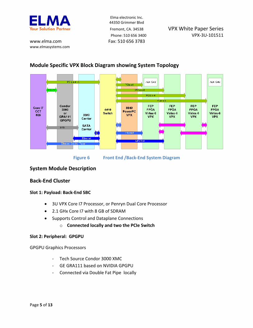
VPX FPGA Carrier Shown with FMC Front End Module
Central to the FPGA architecture is a 3U VPX FPGA (FEP) carrier. The carrier card contains a Xylinx Virtex‐6 Class FPGA with support resources. The FPGA is connected to a VITA 57.1 FMC Site, providing I/O interface to the FPGA. In additional to the FMC, support resources are included on the carrier to support the FPGA. Two Banks of DDR3‐800 memory provide local storage. Facilities required to implement multiple FPGA Bitstreams are included on the card. Further, (MB) of high speed Static SRAM is supported.
Figure 8 Virtex‐6 Based 3U Open VPX FPGA Carrier with FMC Site
The Front End Processor Carrier is interconnected via the VPX bus typically using Fat pipes. Backplanes are available to allow user defined interconnect via cables, or implement the mesh Interconnect shown in Figure 9.
The data plane connection is made via a PCIe Gen 1 x 4 Fat Pipe. This may be a Gen 2 connection if the appropriate speed grade FPGA is selected. The control plane connection can be made via 1000BX Ethernet implemented via the FPGA.

Elma electronic Inc. 44350 Grimmer Blvd
Fremont, CA. 34538 VPX White Paper Series Phone: 510 656 3400 VPX‐3U‐101511
www.elma.com Fax: 510 656 3783 www.elmasystems.com
Page 9 of 13
Table 1 FPGA Feature Comparison
Figure 9 Typical Engineering Kit Pods showing connection to FPGA carrier via JTAG
Elma electronic Inc. 44350 Grimmer Blvd
Fremont, CA. 34538 VPX White Paper Series Phone: 510 656 3400 VPX‐3U‐101511
www.elma.com Fax: 510 656 3783 www.elmasystems.com
Page 10 of 13
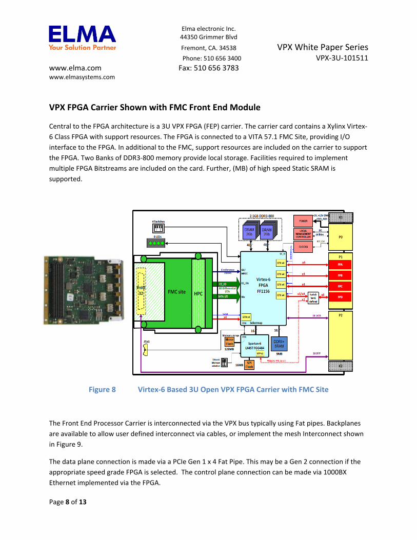
BKP3‐CEN09‐15.2.17‐1
Figure 10 Dual Cluster Central Switched Backplane with Expansion Mesh
Backplane Flexibility
The Front‐End/Back‐End Architecture shown can be configured with payload cards as necessary. The backplane is versatile and is available in three configurations to support uncommitted FPGA interconnect via Meritec cables or via embedded mesh. A third configuration supports a wide local interconnect and routing specific to GE Single Board Computers. Control Plane interconnect is supported via 1000Base‐T in this version.

Elma electronic Inc. 44350 Grimmer Blvd
Fremont, CA. 34538 VPX White Paper Series Phone: 510 656 3400 VPX‐3U‐101511
www.elma.com Fax: 510 656 3783 www.elmasystems.com
Page 11 of 13
Figure 11 GE GPGPU Version of the Dual Cluster Backplane

Elma electronic Inc. 44350 Grimmer Blvd
Fremont, CA. 34538 VPX White Paper Series Phone: 510 656 3400 VPX‐3U‐101511
www.elma.com Fax: 510 656 3783 www.elmasystems.com
Page 12 of 13
SLT3
-PER
-1F-
14.3
.2SL
T3-S
TO-2
U-1
4.5.
1
Figure 12 Open VPX Backplane Diagram of GE GPGPU Backplane Version
Summary
Elma is dedicated to support Open VPX systems architecture through standard application platforms. The Dual Cluster FPGA Development Platform, provides a architecture suitable for development of many FPGA based system applications. Elma can provide this platform with and without Payload Cards. The chassis supports boards from the following vendor:
‐ Concurrent Technologies: SBC, and Switch ‐ GE Intelligent Platform: SBCs ‐ Delphi Engineer: FMC Products for FPGA Carriers ‐ Curtis Wright: FPGA ‐ Interface Concept: SBC, and FPGA, and Switch ‐ X‐Embedded: Storage Carriers and XMC Carrier

Elma electronic Inc. 44350 Grimmer Blvd
Fremont, CA. 34538 VPX White Paper Series Phone: 510 656 3400 VPX‐3U‐101511
www.elma.com Fax: 510 656 3783 www.elmasystems.com
Page 13 of 13
Elma can deliver the card payloads integrated, providing a rapid system development capability for the end user. Initial integration of the OpenVPX compatible cards is provided by Elma, allowing the platform to be productive when received for development