Embed Size (px)
Citation preview
Final Report Contract No.: FA9550-08-1-0070 Xuejun Lu, UMass Lowell
i
DEVELOPING INFRARED (IR) TRANSPARENT CONDUCTIVE
ELECTRODE TECHNOLOGY FOR MULTI-FUNCTIONAL INFRARED
(IR) SENSING
Final Report
Reporting Period: February 15, 2008— February 28, 2011
Contract No.: FA9550-08-1-0070
Dr. Xuejun Lu
Title: Associate professor
Email: [email protected]
Phone: 978-934-3359
Fax: 978-934-3027
Report to:
Dr. Kitt C Reinhardt
AFOSR
875 North Randolph Street
Arlington, VA 22203
Final Report Contract No.: FA9550-08-1-0070 Xuejun Lu, UMass Lowell
ii
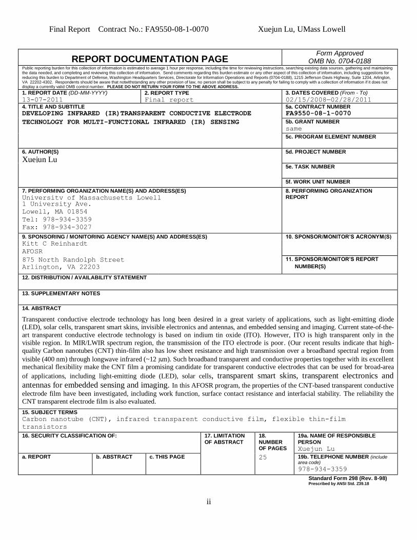
REPORT DOCUMENTATION PAGE Form Approved
OMB No. 0704-0188 Public reporting burden for this collection of information is estimated to average 1 hour per response, including the time for reviewing instructions, searching existing data sources, gathering and maintaining the data needed, and completing and reviewing this collection of information. Send comments regarding this burden estimate or any other aspect of this collection of information, including suggestions for reducing this burden to Department of Defense, Washington Headquarters Services, Directorate for Information Operations and Reports (0704-0188), 1215 Jefferson Davis Highway, Suite 1204, Arlington, VA 22202-4302. Respondents should be aware that notwithstanding any other provision of law, no person shall be subject to any penalty for failing to comply with a collection of information if it does not display a currently valid OMB control number. PLEASE DO NOT RETURN YOUR FORM TO THE ABOVE ADDRESS.
1. REPORT DATE (DD-MM-YYYY)
13-07-2011 2. REPORT TYPE Final report
3. DATES COVERED (From - To)
02/15/2008—02/28/2011 4. TITLE AND SUBTITLE
DEVELOPING INFRARED (IR)TRANSPARENT CONDUCTIVE ELECTRODE
TECHNOLOGY FOR MULTI-FUNCTIONAL INFRARED (IR) SENSING
5a. CONTRACT NUMBER
FA9550-08-1-0070
TECHNOLOGY FOR MULTI-FUNCTIONAL INFRARED (IR) SENSING 5b. GRANT NUMBER
same
5c. PROGRAM ELEMENT NUMBER
6. AUTHOR(S)
Xuejun Lu
5d. PROJECT NUMBER
5e. TASK NUMBER
5f. WORK UNIT NUMBER
7. PERFORMING ORGANIZATION NAME(S) AND ADDRESS(ES)
University of Massachusetts Lowell
AND ADDRESS(ES)
8. PERFORMING ORGANIZATION REPORT NUMBER 1 University Ave.
Lowell, MA 01854
Tel: 978-934-3359
Fax: 978-934-3027
9. SPONSORING / MONITORING AGENCY NAME(S) AND ADDRESS(ES) 10. SPONSOR/MONITOR’S ACRONYM(S) Kitt C Reinhardt
AFOSR
875 North Randolph Street 11. SPONSOR/MONITOR’S REPORT
Arlington, VA 22203 NUMBER(S)
12. DISTRIBUTION / AVAILABILITY STATEMENT
13. SUPPLEMENTARY NOTES
14. ABSTRACT
Transparent conductive electrode technology has long been desired in a great variety of applications, such as light-emitting diode
(LED), solar cells, transparent smart skins, invisible electronics and antennas, and embedded sensing and imaging. Current state-of-the-
art transparent conductive electrode technology is based on indium tin oxide (ITO). However, ITO is high transparent only in the
visible region. In MIR/LWIR spectrum region, the transmission of the ITO electrode is poor. (Our recent results indicate that high-
quality Carbon nanotubes (CNT) thin-film also has low sheet resistance and high transmission over a broadband spectral region from
visible (400 nm) through longwave infrared (~12 m). Such broadband transparent and conductive properties together with its excellent mechanical flexibility make the CNT film a promising candidate for transparent conductive electrodes that can be used for broad-area
of applications, including light-emitting diode (LED), solar cells, transparent smart skins, transparent electronics and
antennas for embedded sensing and imaging. In this AFOSR program, the properties of the CNT-based transparent conductive
electrode film have been investigated, including work function, surface contact resistance and interfacial stability. The reliability the
CNT transparent electrode film is also evaluated.
15. SUBJECT TERMS Carbon nanotube (CNT), infrared transparent conductive film, flexible thin-film
transistors
16. SECURITY CLASSIFICATION OF:
17. LIMITATION
OF ABSTRACT
18.
NUMBER OF PAGES
19a. NAME OF RESPONSIBLE
PERSON Xuejun Lu
a. REPORT
b. ABSTRACT
c. THIS PAGE
25
19b. TELEPHONE NUMBER (include area code)
978-934-3359
Standard Form 298 (Rev. 8-98) Prescribed by ANSI Std. Z39.18
Final Report Contract No.: FA9550-08-1-0070 Xuejun Lu, UMass Lowell
iii
TABLE OF CONTENTS
TABLE OF CONTENTS ....................................................................................................... III
LIST OF TABLES ................................................................................................................. VI
1. APPLICATIONS AND BACKGROUND ................................................................. 1
2. DETILED RESEARCH REPORT ............................................................................ 2
2.1 Took SEM image and measured the IR-transmission spectrum of the CNT film......2
2.2 Determined the work function the CNT film ...........................................................3
2.3 Determined the contact resistance and the mobility of the CNT film .......................4
2.4 Determined the transmission of the CNT film and its sheet resistance .....................5
2.5 Investigated the doping of different chemical function groups and their effects on
the work function of CNTs ......................................................................................7
2.6 Measured the CNT performance under different chemicals ................................... 10
2.7 Measured the CNT performance under different temperatures ............................... 12
2.8 Designed a MEMS based comb filter with integrated LWIR photodetector ........... 12
2.8 Analyze the linearity of the all-printed transistors ................................................. 14
2.9 Evaluate reliability of the CNT film and develop reliability enhancement techniques
............................................................................................................................. 17
3. PERSONNEL SUPPORTED ................................................................................... 19
4. PUBLICATIONS ...................................................................................................... 19
6. NEW DISCOVERIES, INVENTIONS, OR PATENT DISCLOSURES ................ 20
7. HONORS/AWARDS ................................................................................................ 20
REFEENCES .......................................................................................................................... 20
Final Report Contract No.: FA9550-08-1-0070 Xuejun Lu, UMass Lowell
iv
List of figures
Figure 1. (a) SEM image and (b), IR-transmission spectrum of the CNT film (pink curve), and
transmission spectrum of an ITO film (blue curve). The CNT film shows a high
transmission of > 95% from 7µm to 10µm and from 11µm to 12µm and a low sheet
resistance of 200Ω/sq. .................................................................................................2
Figure 2. (a) Resistances between randomly chosen points on an ITO glass; (b) Etching away
ITO stripes, recoated with CNT films, and re-measured the resistances between the
pre-chosen points. .......................................................................................................3
Figure 3, (a) Schematic setup for the CNT work function measurement; (b) Expected I-V curve
of the CNT-metal Schottky barrier; (c), Band diagrams of Aluminum and the p-type
doped CNT film; (d) – (f), The band diagrams of the Al-CNT film Schottky barrier at
zero-bias, forward and reverse bias, respectively. ........................................................3
Figure 4. I-V Characteristics of the CNT-metal Schottky barrier. The CNT-metal Schottky diode
turns on at ~ 0.5V. The Fermi-level of the CNF film is determined to be ~ 4.8eV. .......4
Figure 5, I-V curve of CNT film. .................................................................................................5
Figure 6. Transmission spectrum of the CNT films. A transmission of over 40% were obtained at
a sheet resistance value of 146 Ω. . ..............................................................................6
Figure 7, Transmission of CNT film at 550nm as a function of sheet resistance...........................6
Figure 8, Schematic view of the I-V characteristics measurement. ...............................................7
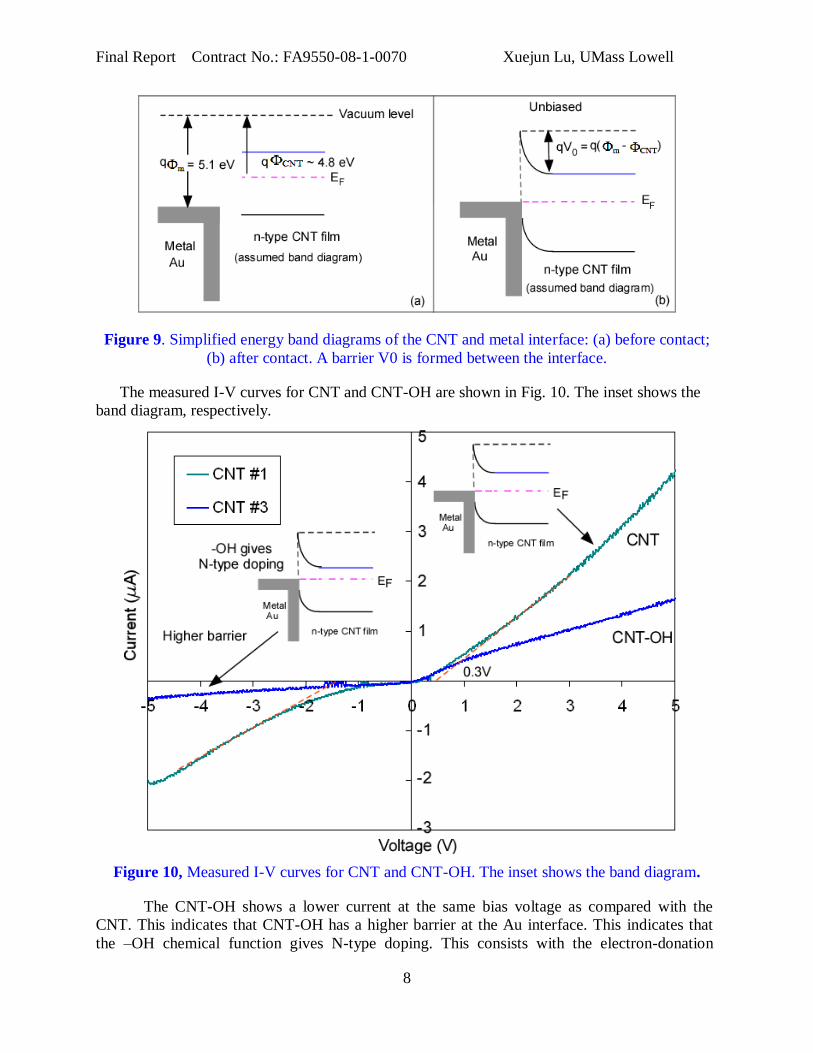
Figure 9. Simplified energy band diagrams of the CNT and metal interface: (a) before contact;
(b) after contact. A barrier V0 is formed between the interface. ...................................8
Figure 10, Measured I-V curves for CNT and CNT-OH. The inset shows the band diagram. .......8
Figure 11, Measured I-V curves for CNT-COOH. The inset shows the band diagram. .................9
Figure 12, Current conduction of the CNT film in a small chamber with Alcohol (CH3CH2-OH)
at different time intervals after the CNT film is put into the Alcohol chamber. .......... 10
Figure 13, I-V curves at different time intervals after the CNT film is taken out of the Alcohol
chamber. ................................................................................................................... 11
Figure 14, I-V curves before the CNT film is put into the water chamber and after it is taken out
of the water chamber. ................................................................................................ 11
Figure 15, I-V curves of the CNT film under different temperatures varying from room
temperature 20 C to 100 C. ..................................................................................... 12
Figure 16, Schematic structure of the hyper-spectral IR Photodetector with integrated tunable
filter. ......................................................................................................................... 13
Figure 17, Schematic structure of the double cavity comb filter. ................................................ 14
Figure 18, Simulated transmission spectrum of the double cavity comb filter. ........................... 14
Figure 19, Measured Ids v.s. Vds at different gate voltages. ...................................................... 15
Figure 20. Drain current ID v.s. VG curves at the source-drain voltage VDS of -0.3V. A high
ON/OFF ratio of ~ 103 is obtained. ............................................................................ 16
Final Report Contract No.: FA9550-08-1-0070 Xuejun Lu, UMass Lowell
v
Figure 21. Logarithmic plots of the ID v.s. VG curves in the region III of Fig. 20. The dashed lines
indicated linear dependence of natural logarithm of the drain current ln(ID) on the gate
voltage VG. ................................................................................................................ 17
Figure 22, Schematic of the interfacial work of adhesion measurement ..................................... 18
Figure 23. Adhesion the CNT films with different chemical function groups. The CNT films
show excellent adhesion. This can be attributed to the high density CNT networks. .. 18
Final Report Contract No.: FA9550-08-1-0070 Xuejun Lu, UMass Lowell
vi
LIST OF TABLES
Table 1, CNT solutions under test ...............................................................................................7
Table 2, Electron-withdrawing and electron-donating chemical function groups .........................9
Final Report Contract No.: FA9550-08-1-0070 Xuejun Lu, UMass Lowell
1
1. APPLICATIONS AND BACKGROUND
Transparent conductive electrode technology has long been desired in a great variety of
applications, such as light-emitting diode (LED), solar cells, transparent smart skins, invisible
electronics and antennas, and embedded sensing and imaging. Particularly, transparent electrodes
in IR spectrum region can be integrated with IR sensors and focal plane array (FPA) to provide
multi-functionalities such as transparent electrical interconnects for on-chip signal processing
and tunable filters for pixel-wise embedded spectral analysis. Such integrated functionalities
would not only enhance the pixel-level sensing and processing capabilities (smart pixel), but also
greatly reduce the communication traffic loads between the image sensors and the subsequent
image processing electronics. This would enable high-throughput IR sensing and target detection
with enhanced characterization and discrimination capabilities.
The state-of-the-art transparent conductive electrode technology is based on indium tin oxide
(ITO) [1-4]. While the ITO based transparent conductive electrodes are extensively used in LCD
display, solar cells and LEDs, there are a few issues related to the ITO technology. One is that
ITO has poor mechanical flexibility and is brittle. The other is that high quality ITO films can
only be obtained at substrate temperature over 300 C. Depositing ITO films at low substrate
temperatures (below 300 C) results in opaque films with high sheet resistance (> 500 Ohms/sq)
[2]. The poor mechanical flexibility and high substrate temperature requirement seriously limit
its applications in flexible devices, such as flexible display, organic solar cell, and smart skin
technology. In addition, ITO is transparent only at visible region. It is highly absorptive at
middle infrared (MIR, 3-5µm) and longwave infrared (LWIR, 8-12µm) regions, and are thus not
suitable for applications in MIR and LWIR spectral region.
Carbon nanotubes (CNT) [5-9], as a new material with exceptional aspect ratio and great
mechanical flexibility, have shown excellent thermal conductivity and extremely high field-
effect mobility of over 100,000 cm2/Vs [6-9]. Carbon nanotubes (CNT), a novel material with
great mechanical flexibility, have shown excellent thermal conductivity and extremely high
field-effect mobility. Our recent results indicate that high-quality CNT thin-film also has low
sheet resistance and high transmission over a broadband spectral region from visible (400 nm)
through longwave infrared (~12 m). Such broadband transparent and conductive properties
together with its excellent mechanical flexibility make the CNT film a promising candidate for
transparent conductive electrodes that can be used for broad-area of applications, including light-
emitting diode (LED), solar cells, transparent smart skins, transparent electronics and antennas
for embedded sensing and imaging.
Despite the promising characteristics of the CNT transparent conductive film, electrical
parameters of the CNT film, such as work function and contact resistance on different
semiconductor surfaces such as Si, GaAs and InP, are not available. Such parameters are critical
in achieving good Ohmic contact on these semiconductor surfaces. Also highly desired is to
evaluate the reliabilities of the CNT film and develop reliability enhancement techniques,
especially for space applications. The goal of this research is to specifically address these issues.
The objectives of the AFOSR research program proposed research are to:
(1) Obtain electrical parameters of the CNT film, including work function and contact
resistance of the CNT film on different semiconductors.
(2) Develop effective doping and transmission spectrum window tuning and engineering
techniques.
Final Report Contract No.: FA9550-08-1-0070 Xuejun Lu, UMass Lowell
2
(3) Evaluate reliability of the CNT film and develop reliability enhancement techniques.
In the AFOSR research, we have performed the following three research tasks, plus a report task:
Task 1: Obtain detailed electrical and spectrum parameters of the CNT film
Task 2: Develop effective doping and transmission spectrum window tuning and
engineering techniques
Task 3: Evaluate reliability of the CNT film and develop reliability enhancement
techniques
Task 4: Reporting
2. DETILED RESEARCH REPORT
2.1 Took SEM image and measured the IR-transmission spectrum of the CNT film
Fig. 1 (a) shows the SEM image and the IR-transmission spectrum of the CNT film (pink
curve), respectively. The IR-transmission spectrum ITO film is also shown in Fig. 1(b) (blue
curve) for comparison. The CNT film shows a high transmission of > 95% from 7µm to 10µm
and from 11µm to 12µm and a low sheet resistance of 200Ω/sq. Our measurement results are
consistent with published results [10-11]. Such good transmission in IR region and low resistance
provide an unprecedented opportunity to achieve IR transparent conductive electrode.
(a)
(b)
Figure 1. (a) SEM image and (b), IR-transmission spectrum of the CNT film (pink curve), and
transmission spectrum of an ITO film (blue curve). The CNT film shows a high transmission of
> 95% from 7µm to 10µm and from 11µm to 12µm and a low sheet resistance of 200Ω/sq.
To compare the conductivity of the CNT film with that of an ITO film, three points on the
ITO glass were randomly chosen and the resistances between these points were measured to be
RAB = 0.32k Ω, and RBC = 0.30 k Ω, respectively. This is shown in Fig. 2(a). Then these points
are isolated by etching away the ITO within the 0.5 inch-wide stripes between theses points, as
shown in Fig. 3(b). The PI then coated the 0.5 inch-wide stripes with CNT films (Fig. 2(b)) and
re-measured the resistances between these points to be RAB = 1.3k Ω, and RBC = 1.1 k Ω,
respectively. The transmissions of the CNT films were confirmed to be over 95% over the visible
spectrum by a PerkinElmer UV-VIS absorption spectrometer. This experiment demonstrated that
the CNT film is promising for transparent conductive electrode.
Final Report Contract No.: FA9550-08-1-0070 Xuejun Lu, UMass Lowell
3
RAB =0.32 KΩ RBC = 0.30 KΩ
A BC
RBC = 1.1 KΩRAB = 1.3 KΩ
A BC
A BC
(a) (b)
Figure 2. (a) Resistances between randomly chosen points on an ITO glass; (b) Etching away
ITO stripes, recoated with CNT films, and re-measured the resistances between the pre-chosen
points.
2.2 Determined the work function the CNT film
In this research period, we have performed research to determined the work function of CNT
film to. The schematic of the proposed measurement setup is shown in Fig. 3(a).
Figure 3, (a) Schematic setup for the CNT work function measurement; (b) Expected I-V curve
of the CNT-metal Schottky barrier; (c), Band diagrams of Aluminum and the p-type doped CNT
film; (d) – (f), The band diagrams of the Al-CNT film Schottky barrier at zero-bias, forward and
reverse bias, respectively.
Final Report Contract No.: FA9550-08-1-0070 Xuejun Lu, UMass Lowell
4
The setup is to measure the I-V curve of the Schottky barrier formed between aluminum(Al)
with known work function s = 4.3eV and the CNT film. From the I-V curve (Fig. 3(b)), we
measured the threshold voltage of the Schottky barrier V0, which is related to the work function
of the metal and that of the CNT film by:
)(0 mCNTqqV , (1)
The work function of the CNT film can thus be obtained by:
mCNT V0 , (2)
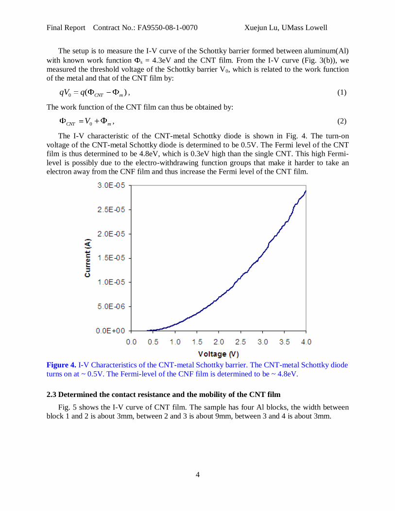
The I-V characteristic of the CNT-metal Schottky diode is shown in Fig. 4. The turn-on
voltage of the CNT-metal Schottky diode is determined to be 0.5V. The Fermi level of the CNT
film is thus determined to be 4.8eV, which is 0.3eV high than the single CNT. This high Fermi-
level is possibly due to the electro-withdrawing function groups that make it harder to take an
electron away from the CNF film and thus increase the Fermi level of the CNT film.
Figure 4. I-V Characteristics of the CNT-metal Schottky barrier. The CNT-metal Schottky diode
turns on at ~ 0.5V. The Fermi-level of the CNF film is determined to be ~ 4.8eV.
2.3 Determined the contact resistance and the mobility of the CNT film
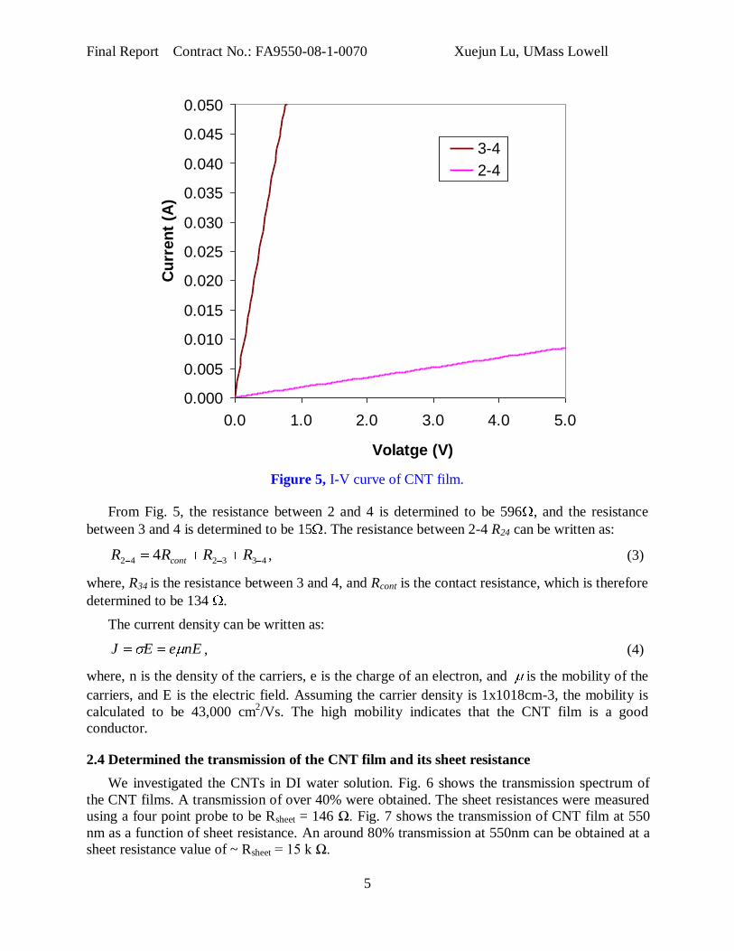
Fig. 5 shows the I-V curve of CNT film. The sample has four Al blocks, the width between
block 1 and 2 is about 3mm, between 2 and 3 is about 9mm, between 3 and 4 is about 3mm.
Final Report Contract No.: FA9550-08-1-0070 Xuejun Lu, UMass Lowell
5
0.000
0.005
0.010
0.015
0.020
0.025
0.030
0.035
0.040
0.045
0.050
0.0 1.0 2.0 3.0 4.0 5.0
Volatge (V)
Cu
rren
t (A
)
3-4
2-4
Figure 5, I-V curve of CNT film.
From Fig. 5, the resistance between 2 and 4 is determined to be 596 , and the resistance
between 3 and 4 is determined to be 15 . The resistance between 2-4 R24 can be written as:
433242 4 RRRR cont , (3)
where, R34 is the resistance between 3 and 4, and Rcont is the contact resistance, which is therefore
determined to be 134 .
The current density can be written as:
nEeEJ , (4)
where, n is the density of the carriers, e is the charge of an electron, and is the mobility of the
carriers, and E is the electric field. Assuming the carrier density is 1x1018cm-3, the mobility is
calculated to be 43,000 cm2/Vs. The high mobility indicates that the CNT film is a good
conductor.
2.4 Determined the transmission of the CNT film and its sheet resistance
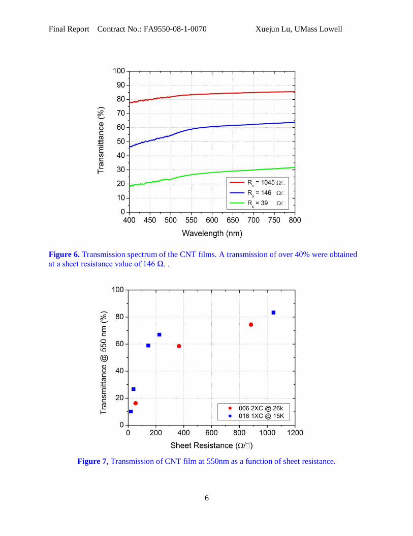
We investigated the CNTs in DI water solution. Fig. 6 shows the transmission spectrum of
the CNT films. A transmission of over 40% were obtained. The sheet resistances were measured
using a four point probe to be Rsheet = 146 Ω. Fig. 7 shows the transmission of CNT film at 550
nm as a function of sheet resistance. An around 80% transmission at 550nm can be obtained at a
sheet resistance value of ~ Rsheet = 15 k Ω.
Final Report Contract No.: FA9550-08-1-0070 Xuejun Lu, UMass Lowell
6
Figure 6. Transmission spectrum of the CNT films. A transmission of over 40% were obtained
at a sheet resistance value of 146 Ω. .
Figure 7, Transmission of CNT film at 550nm as a function of sheet resistance.
Final Report Contract No.: FA9550-08-1-0070 Xuejun Lu, UMass Lowell
7
2.5 Investigated the doping of different chemical function groups and their effects on the
work function of CNTs
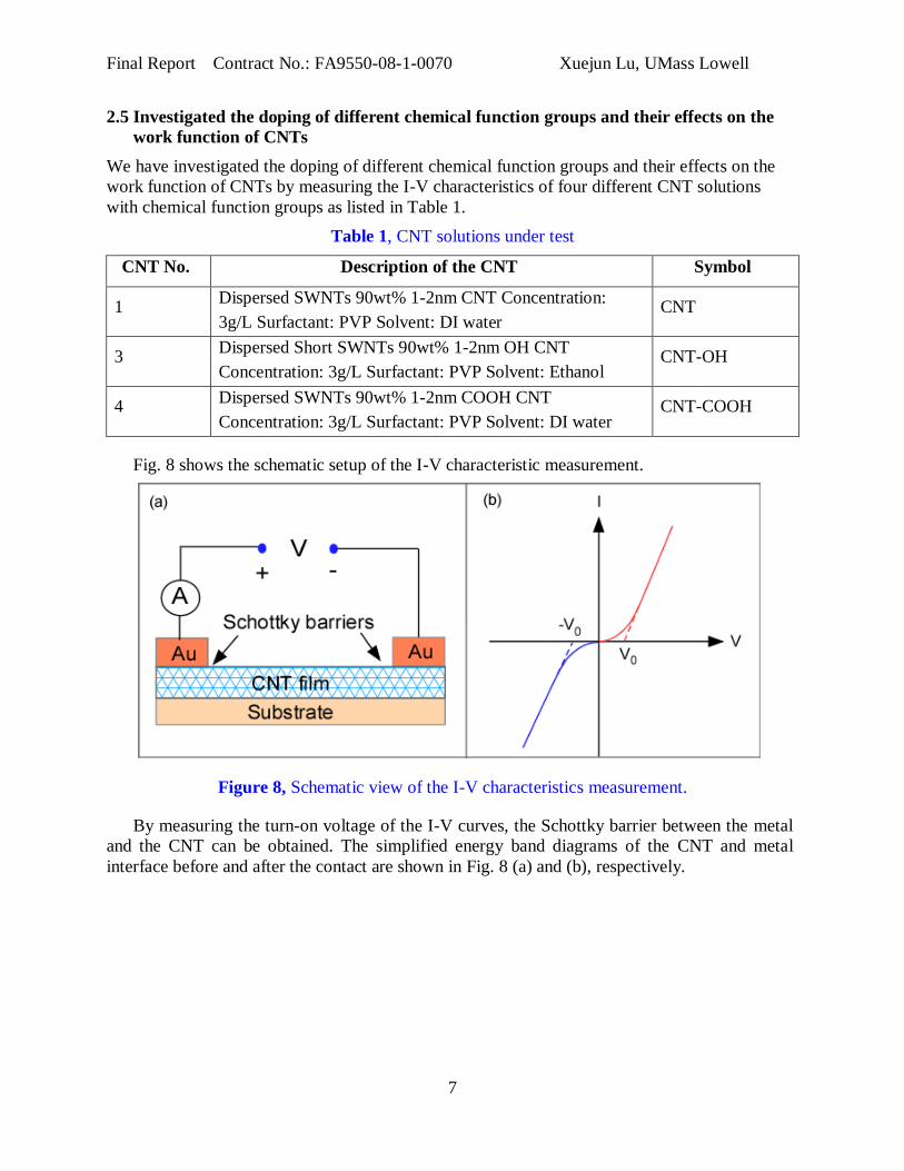
We have investigated the doping of different chemical function groups and their effects on the
work function of CNTs by measuring the I-V characteristics of four different CNT solutions
with chemical function groups as listed in Table 1.
Table 1, CNT solutions under test
CNT No. Description of the CNT Symbol
1 Dispersed SWNTs 90wt% 1-2nm CNT Concentration:
3g/L Surfactant: PVP Solvent: DI water CNT
3 Dispersed Short SWNTs 90wt% 1-2nm OH CNT
Concentration: 3g/L Surfactant: PVP Solvent: Ethanol CNT-OH
4 Dispersed SWNTs 90wt% 1-2nm COOH CNT
Concentration: 3g/L Surfactant: PVP Solvent: DI water CNT-COOH
Fig. 8 shows the schematic setup of the I-V characteristic measurement.
Figure 8, Schematic view of the I-V characteristics measurement.
By measuring the turn-on voltage of the I-V curves, the Schottky barrier between the metal
and the CNT can be obtained. The simplified energy band diagrams of the CNT and metal
interface before and after the contact are shown in Fig. 8 (a) and (b), respectively.
Final Report Contract No.: FA9550-08-1-0070 Xuejun Lu, UMass Lowell
8
Figure 9. Simplified energy band diagrams of the CNT and metal interface: (a) before contact;
(b) after contact. A barrier V0 is formed between the interface.
The measured I-V curves for CNT and CNT-OH are shown in Fig. 10. The inset shows the
band diagram, respectively.
Figure 10, Measured I-V curves for CNT and CNT-OH. The inset shows the band diagram.
The CNT-OH shows a lower current at the same bias voltage as compared with the
CNT. This indicates that CNT-OH has a higher barrier at the Au interface. This indicates that
the –OH chemical function gives N-type doping. This consists with the electron-donation
Final Report Contract No.: FA9550-08-1-0070 Xuejun Lu, UMass Lowell
9
property of the –OH chemical function group. Table 2 shows different chemical function groups
for electron-withdrawing and electron-donating.
Table 2, Electron-withdrawing and electron-donating chemical function groups
Electron-withdrawing function groups Electron-donating function groups
-COOR, -COOH, -COR, -CHO, -NO2, -CN
-F, -Cl, -BR, -I, -CF3 (where, R represents the
group -CH3)
-OH, -NH2, -NR2, -SH, -CR3, -OR
(where, R represents the group -CH3)
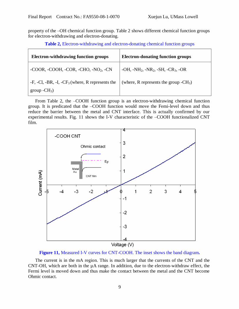
From Table 2, the –COOH function group is an electron-withdrawing chemical function
group. It is predicated that the –COOH function would move the Femi-level down and thus
reduce the barrier between the metal and CNT interface. This is actually confirmed by our
experimental results. Fig. 11 shows the I-V characteristic of the –COOH functionalized CNT
film.
Figure 11, Measured I-V curves for CNT-COOH. The inset shows the band diagram.
The current is in the mA region. This is much larger that the currents of the CNT and the
CNT-OH, which are both in the µA range. In addition, due to the electron-withdraw effect, the
Fermi level is moved down and thus make the contact between the metal and the CNT become
Ohmic contact.
Final Report Contract No.: FA9550-08-1-0070 Xuejun Lu, UMass Lowell
10
This indicates that by functionalize the CNT with electron-donation or withdrawing
chemical function groups, effective Fermi-level tuning can be achieved. Such Femi-level tuning
can be used to change the barrier of the CNT and metal interface and make it either Ohmic
contact or Schottky barrier.
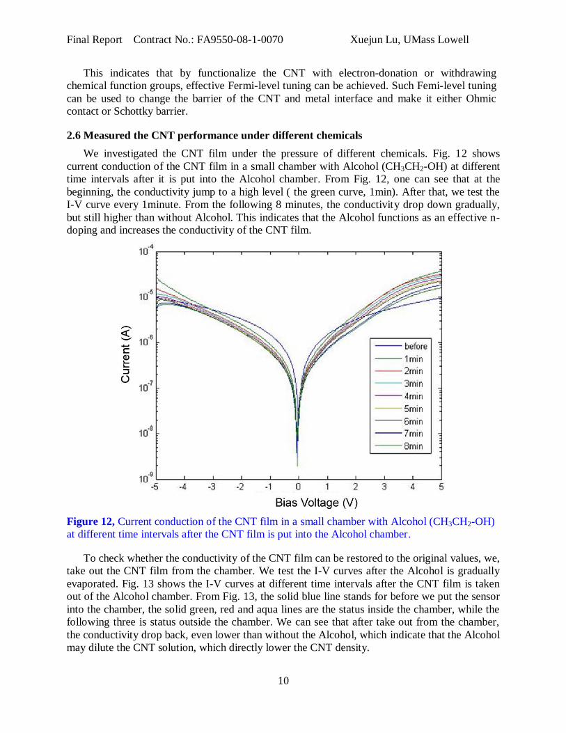
2.6 Measured the CNT performance under different chemicals
We investigated the CNT film under the pressure of different chemicals. Fig. 12 shows
current conduction of the CNT film in a small chamber with Alcohol (CH3CH2-OH) at different
time intervals after it is put into the Alcohol chamber. From Fig. 12, one can see that at the
beginning, the conductivity jump to a high level ( the green curve, 1min). After that, we test the
I-V curve every 1minute. From the following 8 minutes, the conductivity drop down gradually,
but still higher than without Alcohol. This indicates that the Alcohol functions as an effective n-
doping and increases the conductivity of the CNT film.
Figure 12, Current conduction of the CNT film in a small chamber with Alcohol (CH3CH2-OH)
at different time intervals after the CNT film is put into the Alcohol chamber.
To check whether the conductivity of the CNT film can be restored to the original values, we,
take out the CNT film from the chamber. We test the I-V curves after the Alcohol is gradually
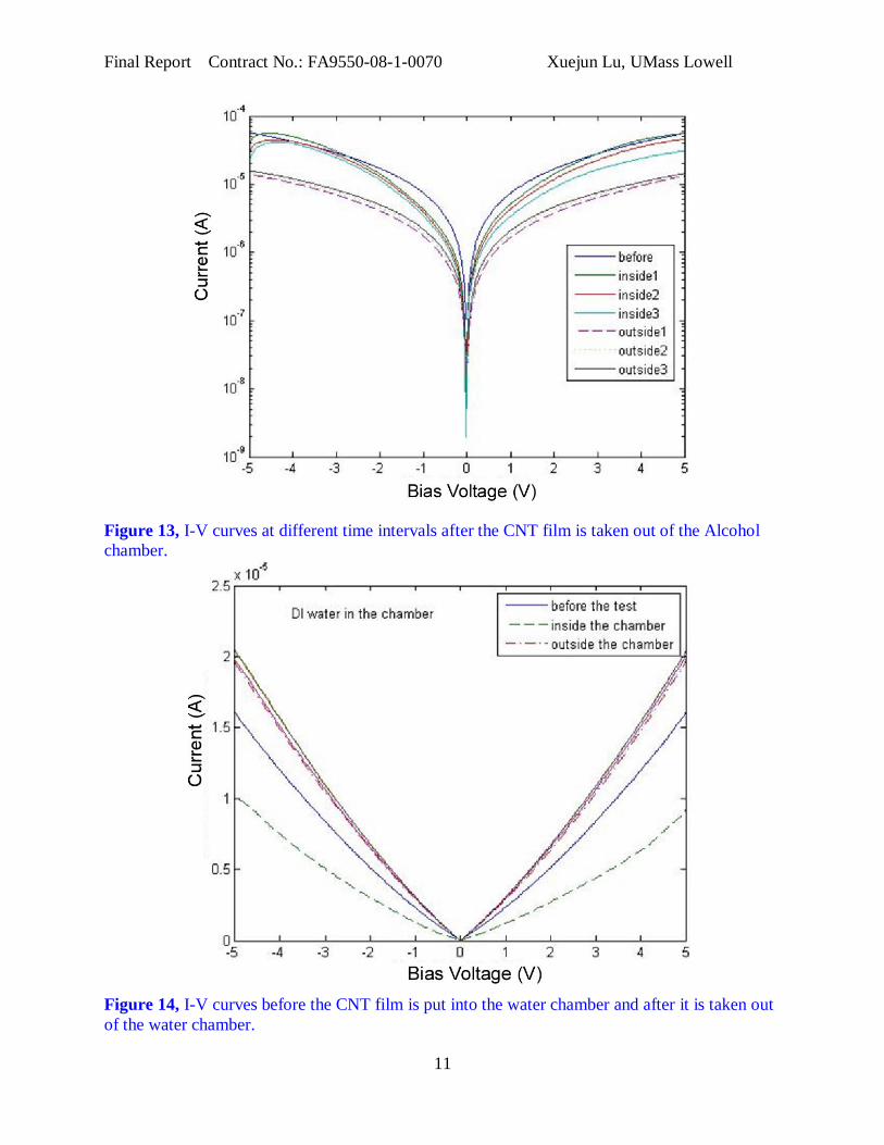
evaporated. Fig. 13 shows the I-V curves at different time intervals after the CNT film is taken
out of the Alcohol chamber. From Fig. 13, the solid blue line stands for before we put the sensor
into the chamber, the solid green, red and aqua lines are the status inside the chamber, while the
following three is status outside the chamber. We can see that after take out from the chamber,
the conductivity drop back, even lower than without the Alcohol, which indicate that the Alcohol
may dilute the CNT solution, which directly lower the CNT density.
Final Report Contract No.: FA9550-08-1-0070 Xuejun Lu, UMass Lowell
11
Figure 13, I-V curves at different time intervals after the CNT film is taken out of the Alcohol
chamber.
Figure 14, I-V curves before the CNT film is put into the water chamber and after it is taken out
of the water chamber.
Final Report Contract No.: FA9550-08-1-0070 Xuejun Lu, UMass Lowell
12
We also tested the CNT film under the pressure of water (H2O). Fig. 14 shows the I-V curves
before the CNT film is put into the water chamber and after it is taken out of the water chamber.
From Fig. 14, one can see that the conductivity of the CNT film is low when it is inside the water
chamber. After it is taken out of the water chamber, the conductivity goes up. This indicates that
H2O will not function as an effective doping for the CNT film and the H2O dilutes the CNT and
thus reduces the conductivity of the CNT film. Since the H2O molecules are small, the
conductivity restores when the H2O molecules are removed from the CNT film.
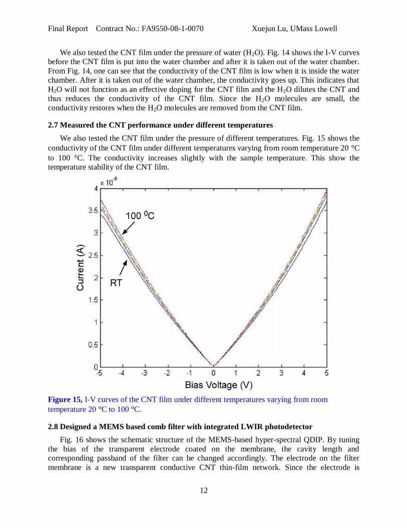
2.7 Measured the CNT performance under different temperatures
We also tested the CNT film under the pressure of different temperatures. Fig. 15 shows the
conductivity of the CNT film under different temperatures varying from room temperature 20 C
to 100 C. The conductivity increases slightly with the sample temperature. This show the
temperature stability of the CNT film.
Figure 15, I-V curves of the CNT film under different temperatures varying from room
temperature 20 C to 100 C.
2.8 Designed a MEMS based comb filter with integrated LWIR photodetector
Fig. 16 shows the schematic structure of the MEMS-based hyper-spectral QDIP. By tuning
the bias of the transparent electrode coated on the membrane, the cavity length and
corresponding passband of the filter can be changed accordingly. The electrode on the filter
membrane is a new transparent conductive CNT thin-film network. Since the electrode is
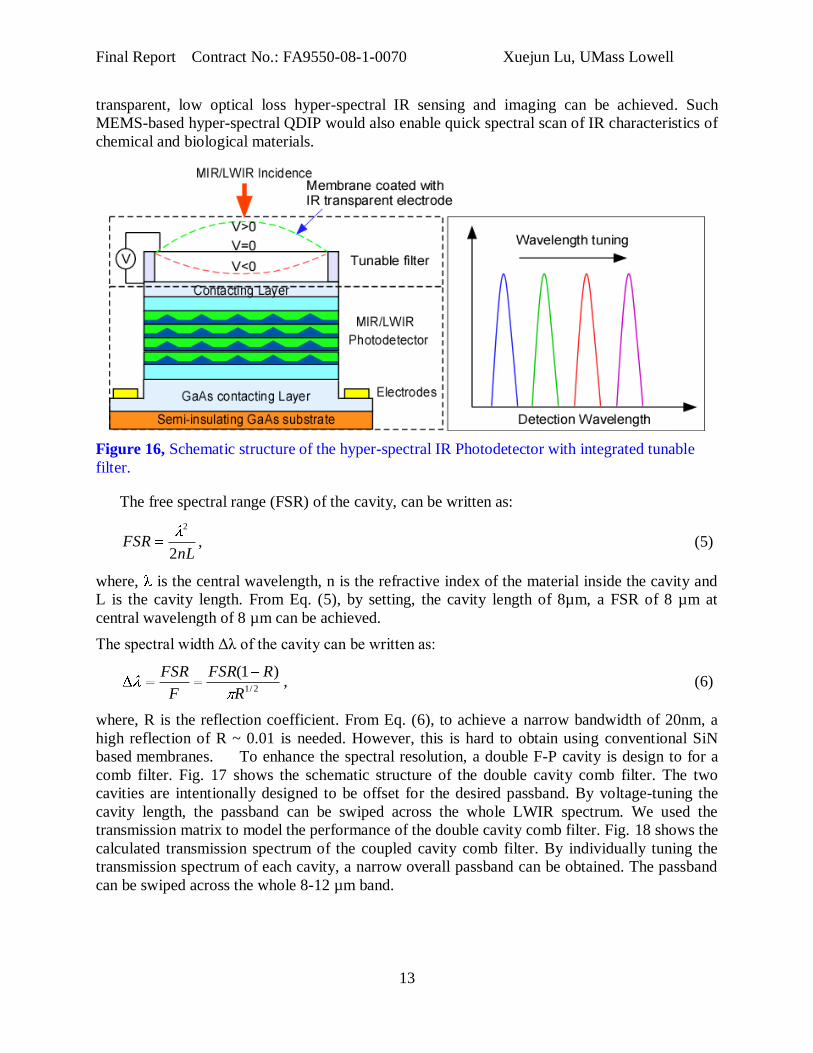
Final Report Contract No.: FA9550-08-1-0070 Xuejun Lu, UMass Lowell
13
transparent, low optical loss hyper-spectral IR sensing and imaging can be achieved. Such
MEMS-based hyper-spectral QDIP would also enable quick spectral scan of IR characteristics of
chemical and biological materials.
Figure 16, Schematic structure of the hyper-spectral IR Photodetector with integrated tunable
filter.
The free spectral range (FSR) of the cavity, can be written as:
nL
FSR2
2
, (5)
where, is the central wavelength, n is the refractive index of the material inside the cavity and
L is the cavity length. From Eq. (5), by setting, the cavity length of 8µm, a FSR of 8 µm at
central wavelength of 8 µm can be achieved.
The spectral width Δλ of the cavity can be written as:
2/1
)1(
R
RFSR
F
FSR, (6)
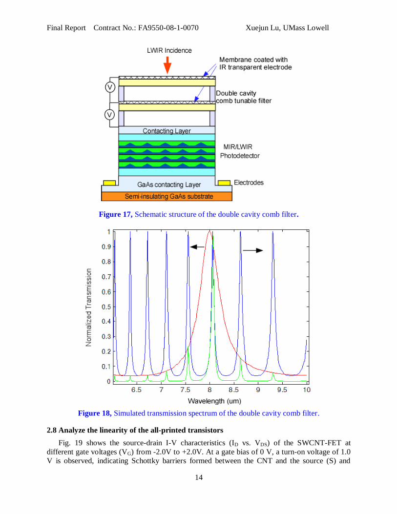
where, R is the reflection coefficient. From Eq. (6), to achieve a narrow bandwidth of 20nm, a
high reflection of R ~ 0.01 is needed. However, this is hard to obtain using conventional SiN
based membranes. To enhance the spectral resolution, a double F-P cavity is design to for a
comb filter. Fig. 17 shows the schematic structure of the double cavity comb filter. The two
cavities are intentionally designed to be offset for the desired passband. By voltage-tuning the
cavity length, the passband can be swiped across the whole LWIR spectrum. We used the
transmission matrix to model the performance of the double cavity comb filter. Fig. 18 shows the
calculated transmission spectrum of the coupled cavity comb filter. By individually tuning the
transmission spectrum of each cavity, a narrow overall passband can be obtained. The passband
can be swiped across the whole 8-12 µm band.
Final Report Contract No.: FA9550-08-1-0070 Xuejun Lu, UMass Lowell
14
Figure 17, Schematic structure of the double cavity comb filter.
Figure 18, Simulated transmission spectrum of the double cavity comb filter.
2.8 Analyze the linearity of the all-printed transistors
Fig. 19 shows the source-drain I-V characteristics (ID vs. VDS) of the SWCNT-FET at
different gate voltages (VG) from -2.0V to +2.0V. At a gate bias of 0 V, a turn-on voltage of 1.0
V is observed, indicating Schottky barriers formed between the CNT and the source (S) and
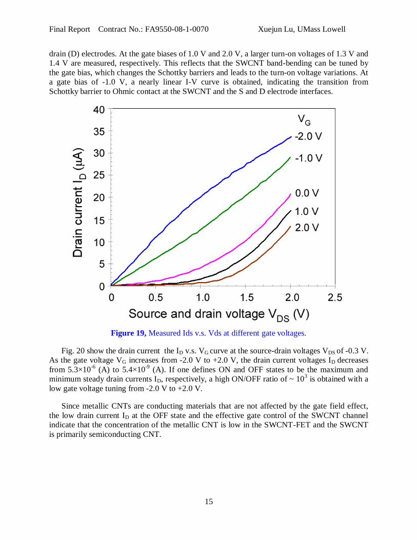
Final Report Contract No.: FA9550-08-1-0070 Xuejun Lu, UMass Lowell
15
drain (D) electrodes. At the gate biases of 1.0 V and 2.0 V, a larger turn-on voltages of 1.3 V and
1.4 V are measured, respectively. This reflects that the SWCNT band-bending can be tuned by
the gate bias, which changes the Schottky barriers and leads to the turn-on voltage variations. At
a gate bias of -1.0 V, a nearly linear I-V curve is obtained, indicating the transition from
Schottky barrier to Ohmic contact at the SWCNT and the S and D electrode interfaces.
Figure 19, Measured Ids v.s. Vds at different gate voltages.
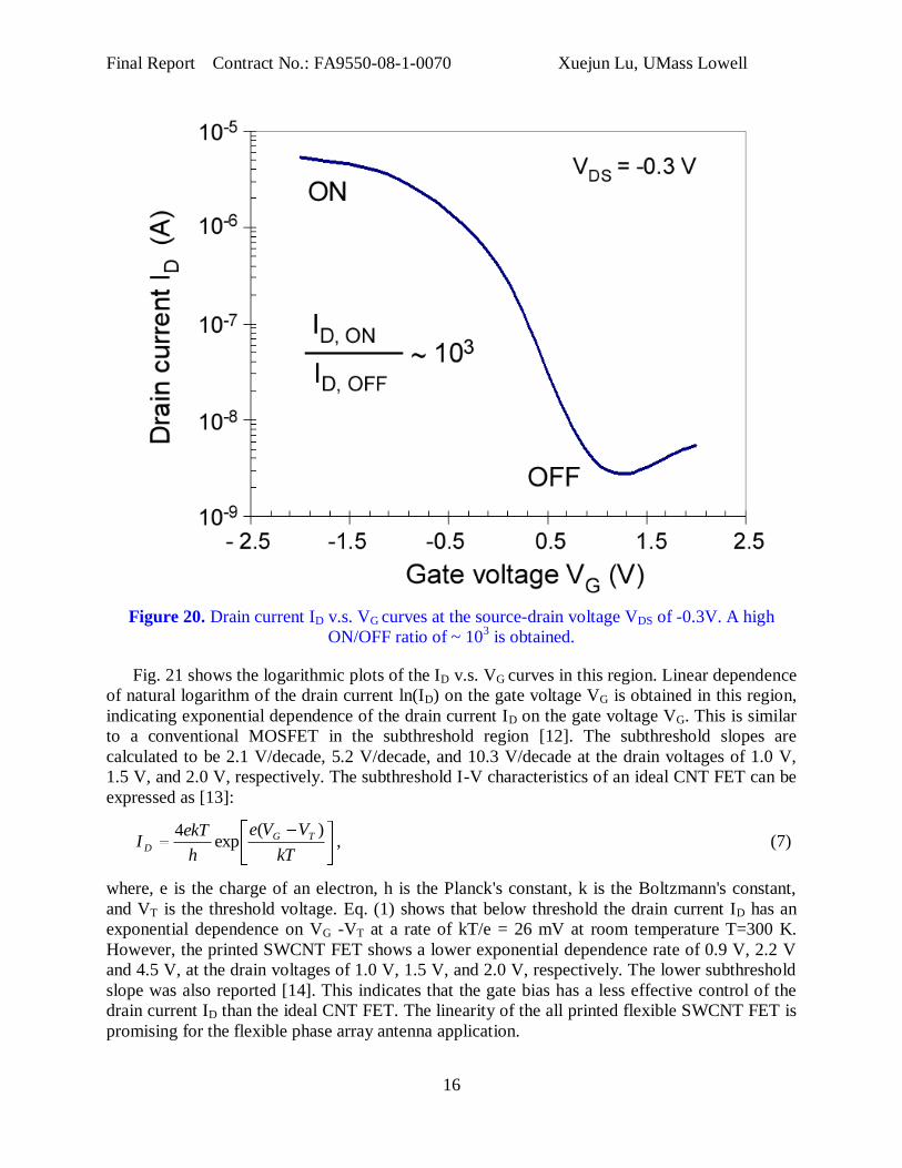
Fig. 20 show the drain current the ID v.s. VG curve at the source-drain voltages VDS of -0.3 V.
As the gate voltage VG increases from -2.0 V to +2.0 V, the drain current voltages ID decreases
from 5.3×10⁻⁶
(A) to 5.4×10⁻⁹
(A). If one defines ON and OFF states to be the maximum and
minimum steady drain currents ID, respectively, a high ON/OFF ratio of ~ 103 is obtained with a
low gate voltage tuning from -2.0 V to +2.0 V.
Since metallic CNTs are conducting materials that are not affected by the gate field effect,
the low drain current ID at the OFF state and the effective gate control of the SWCNT channel
indicate that the concentration of the metallic CNT is low in the SWCNT-FET and the SWCNT
is primarily semiconducting CNT.
Final Report Contract No.: FA9550-08-1-0070 Xuejun Lu, UMass Lowell
16
Figure 20. Drain current ID v.s. VG curves at the source-drain voltage VDS of -0.3V. A high
ON/OFF ratio of ~ 103 is obtained.
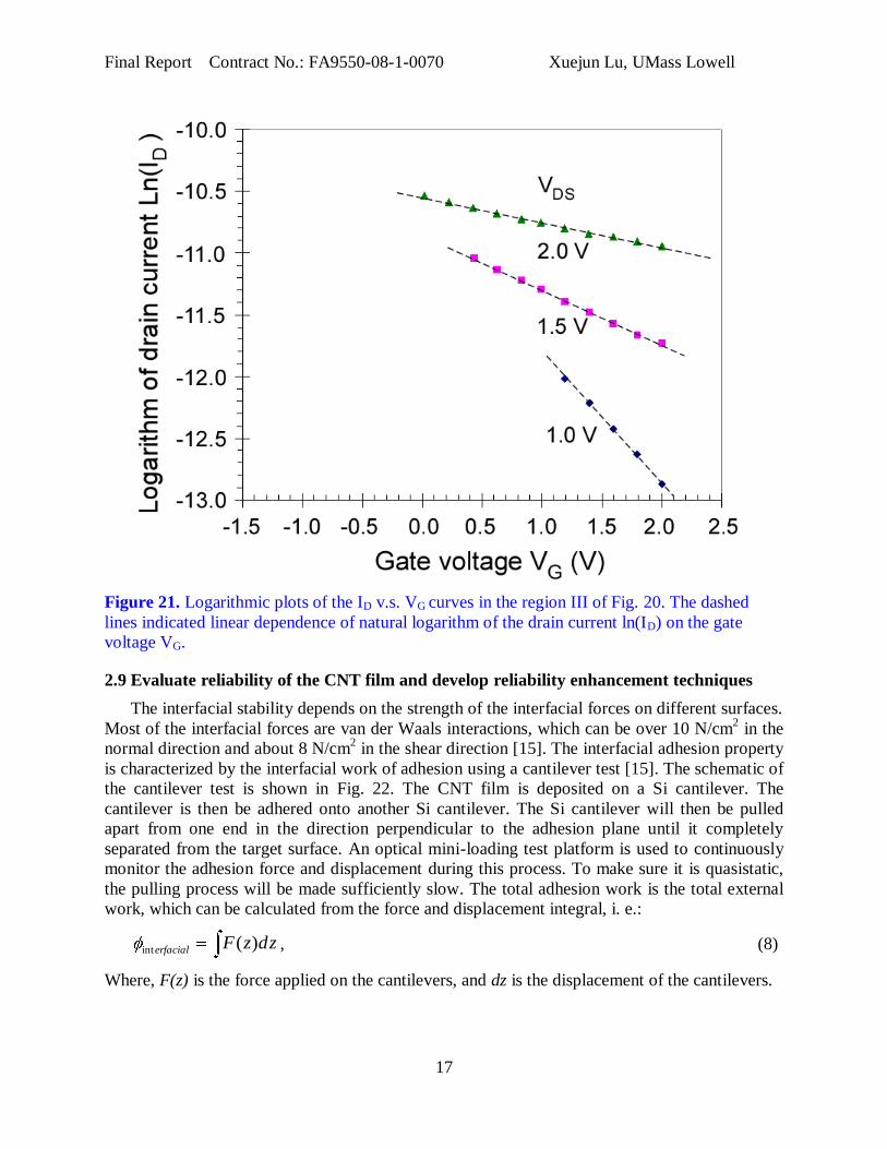
Fig. 21 shows the logarithmic plots of the ID v.s. VG curves in this region. Linear dependence
of natural logarithm of the drain current ln(ID) on the gate voltage VG is obtained in this region,
indicating exponential dependence of the drain current ID on the gate voltage VG. This is similar
to a conventional MOSFET in the subthreshold region [12]. The subthreshold slopes are
calculated to be 2.1 V/decade, 5.2 V/decade, and 10.3 V/decade at the drain voltages of 1.0 V,
1.5 V, and 2.0 V, respectively. The subthreshold I-V characteristics of an ideal CNT FET can be
expressed as [13]:
kT
VVe
h
ekTI TG
D
)(exp
4, (7)
where, e is the charge of an electron, h is the Planck's constant, k is the Boltzmann's constant,
and VT is the threshold voltage. Eq. (1) shows that below threshold the drain current ID has an
exponential dependence on VG -VT at a rate of kT/e = 26 mV at room temperature T=300 K.
However, the printed SWCNT FET shows a lower exponential dependence rate of 0.9 V, 2.2 V
and 4.5 V, at the drain voltages of 1.0 V, 1.5 V, and 2.0 V, respectively. The lower subthreshold
slope was also reported [14]. This indicates that the gate bias has a less effective control of the
drain current ID than the ideal CNT FET. The linearity of the all printed flexible SWCNT FET is
promising for the flexible phase array antenna application.
Final Report Contract No.: FA9550-08-1-0070 Xuejun Lu, UMass Lowell
17
Figure 21. Logarithmic plots of the ID v.s. VG curves in the region III of Fig. 20. The dashed
lines indicated linear dependence of natural logarithm of the drain current ln(ID) on the gate
voltage VG.
2.9 Evaluate reliability of the CNT film and develop reliability enhancement techniques
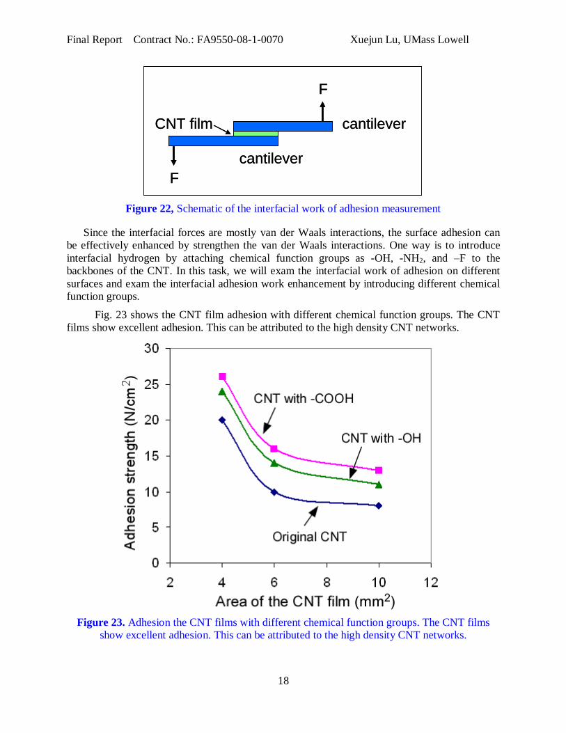
The interfacial stability depends on the strength of the interfacial forces on different surfaces.
Most of the interfacial forces are van der Waals interactions, which can be over 10 N/cm2 in the
normal direction and about 8 N/cm2 in the shear direction [15]. The interfacial adhesion property
is characterized by the interfacial work of adhesion using a cantilever test [15]. The schematic of
the cantilever test is shown in Fig. 22. The CNT film is deposited on a Si cantilever. The
cantilever is then be adhered onto another Si cantilever. The Si cantilever will then be pulled
apart from one end in the direction perpendicular to the adhesion plane until it completely
separated from the target surface. An optical mini-loading test platform is used to continuously
monitor the adhesion force and displacement during this process. To make sure it is quasistatic,
the pulling process will be made sufficiently slow. The total adhesion work is the total external
work, which can be calculated from the force and displacement integral, i. e.:
zdzFerfacial )(int , (8)
Where, F(z) is the force applied on the cantilevers, and dz is the displacement of the cantilevers.
Final Report Contract No.: FA9550-08-1-0070 Xuejun Lu, UMass Lowell
18
F
F
cantilever
cantilever
CNT film
F
F
cantilever
cantilever
CNT film
Figure 22, Schematic of the interfacial work of adhesion measurement
Since the interfacial forces are mostly van der Waals interactions, the surface adhesion can
be effectively enhanced by strengthen the van der Waals interactions. One way is to introduce
interfacial hydrogen by attaching chemical function groups as -OH, -NH2, and –F to the
backbones of the CNT. In this task, we will exam the interfacial work of adhesion on different
surfaces and exam the interfacial adhesion work enhancement by introducing different chemical
function groups.
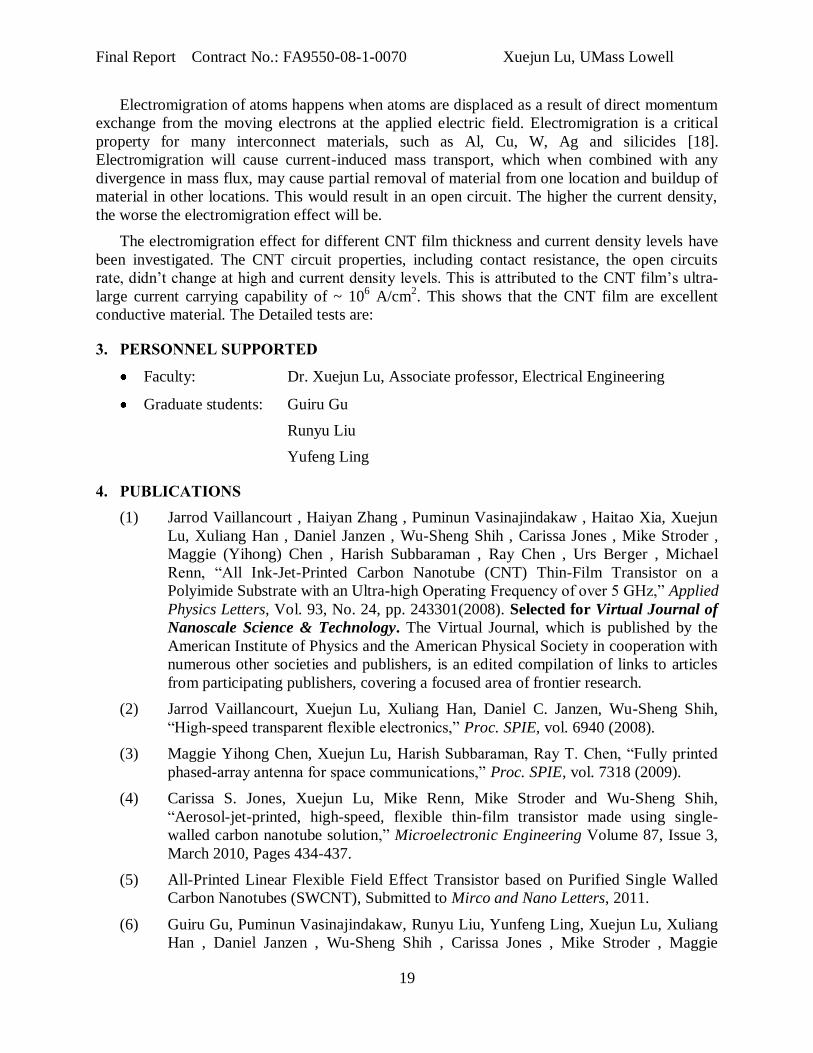
Fig. 23 shows the CNT film adhesion with different chemical function groups. The CNT
films show excellent adhesion. This can be attributed to the high density CNT networks.
Figure 23. Adhesion the CNT films with different chemical function groups. The CNT films
show excellent adhesion. This can be attributed to the high density CNT networks.
Final Report Contract No.: FA9550-08-1-0070 Xuejun Lu, UMass Lowell
19
Electromigration of atoms happens when atoms are displaced as a result of direct momentum
exchange from the moving electrons at the applied electric field. Electromigration is a critical
property for many interconnect materials, such as Al, Cu, W, Ag and silicides [18].
Electromigration will cause current-induced mass transport, which when combined with any
divergence in mass flux, may cause partial removal of material from one location and buildup of
material in other locations. This would result in an open circuit. The higher the current density,
the worse the electromigration effect will be.
The electromigration effect for different CNT film thickness and current density levels have
been investigated. The CNT circuit properties, including contact resistance, the open circuits
rate, didn’t change at high and current density levels. This is attributed to the CNT film’s ultra-
large current carrying capability of ~ 106 A/cm
2. This shows that the CNT film are excellent
conductive material. The Detailed tests are:
3. PERSONNEL SUPPORTED
Faculty: Dr. Xuejun Lu, Associate professor, Electrical Engineering
Graduate students: Guiru Gu
Runyu Liu
Yufeng Ling
4. PUBLICATIONS
(1) Jarrod Vaillancourt , Haiyan Zhang , Puminun Vasinajindakaw , Haitao Xia, Xuejun
Lu, Xuliang Han , Daniel Janzen , Wu-Sheng Shih , Carissa Jones , Mike Stroder ,
Maggie (Yihong) Chen , Harish Subbaraman , Ray Chen , Urs Berger , Michael
Renn, ―All Ink-Jet-Printed Carbon Nanotube (CNT) Thin-Film Transistor on a
Polyimide Substrate with an Ultra-high Operating Frequency of over 5 GHz,‖ Applied
Physics Letters, Vol. 93, No. 24, pp. 243301(2008). Selected for Virtual Journal of
Nanoscale Science & Technology. The Virtual Journal, which is published by the
American Institute of Physics and the American Physical Society in cooperation with
numerous other societies and publishers, is an edited compilation of links to articles
from participating publishers, covering a focused area of frontier research.
(2) Jarrod Vaillancourt, Xuejun Lu, Xuliang Han, Daniel C. Janzen, Wu-Sheng Shih,
―High-speed transparent flexible electronics,‖ Proc. SPIE, vol. 6940 (2008).
(3) Maggie Yihong Chen, Xuejun Lu, Harish Subbaraman, Ray T. Chen, ―Fully printed
phased-array antenna for space communications,‖ Proc. SPIE, vol. 7318 (2009).
(4) Carissa S. Jones, Xuejun Lu, Mike Renn, Mike Stroder and Wu-Sheng Shih,
―Aerosol-jet-printed, high-speed, flexible thin-film transistor made using single-
walled carbon nanotube solution,‖ Microelectronic Engineering Volume 87, Issue 3,
March 2010, Pages 434-437.
(5) All-Printed Linear Flexible Field Effect Transistor based on Purified Single Walled
Carbon Nanotubes (SWCNT), Submitted to Mirco and Nano Letters, 2011.
(6) Guiru Gu, Puminun Vasinajindakaw, Runyu Liu, Yunfeng Ling, Xuejun Lu, Xuliang
Han , Daniel Janzen , Wu-Sheng Shih , Carissa Jones , Mike Stroder , Maggie
Final Report Contract No.: FA9550-08-1-0070 Xuejun Lu, UMass Lowell
20
(Yihong) Chen , Harish Subbaraman , Ray Chen , Urs Berger , Michael Renn, ―All-
Printed Thin-film Transistor (TFT) based on Purified Single Walled Carbon
Nanotubes (SWCNT) with Linear Response,‖ Journal of Nanotechnology, Accepted
for publication, 2011.
6. NEW DISCOVERIES, INVENTIONS, OR PATENT DISCLOSURES
None
7. HONORS/AWARDS
IDTechEx, Academic Research and Development Award 2009.
REFEENCES
[1] C. A. Pan and T. P. Ma, "High-Quality Transparent Conductive Indium Oxide Films
Prepared by Thermal Evaporation," Appl. Phys. Lett., vol. 37, pp. 163-165 (1980).
[2] Hamberg, A. Hjortsberg, and C. G. Granqvist, "High Quality Transparent Heat Reflector
of Reactively Evaporated Indium Tin Oxide," Appl. Phys. Lett. 40, 362-364 (1982).
[3] J. P. Zheng and H. S. Kwok, ―Low resistivity indium tin oxide films by pulsed laser
deposition,‖ Appl. Phys. Lett., vol. 63, pp. 1-3 (1993).
[4] C. G. Granqvist, ―Transparent conductive electrodes for electrochromic devices: A
review,‖ Applied Physics A: Materials Science & Processing, vol. 57, pp. 19-24 (1993).
[5] S. J. Tans, A. R. M. Verschueren, and C. Dekker, ―Room temperature transistor based on a
single carbon nanotube,‖ Nature, vol. 393, pp. 49-52, 1998.
[6] T. Durkop, S. A. Getty, E. Cobas, and M. S. Fuhrer, ―Extraordinary mobility in
semiconducting carbon nanotubes‖, Nano Letters, vol. 4, pp. 35-39, 2004.
[7] K. Bradley, J. P. Gabriel, and G. Gruner, ―Flexible nanotube electronics,‖ Nano Letters,
vol. 3, pp. 1353-1355, 2003.
[8] E. Artukovic, M. Kaempgen, D. S. Hecht, S. Roth, and G. Gruner, ―Transparent and
flexible carbon nanotube transistors,‖ Nano Letters, vol. 5, pp. 757-760, 2005.
[9] T. Durkop, S. A. Getty, E. Cobas, and M. S. Fuhrer, ―Extraordinary mobility in
semiconducting carbon nanotubes‖, Nano Letters, vol. 4, pp. 35-39, 2004.
[10] Z. Wu, Z. Chen, X. Du, and J. Logan, ―Transparent, Conductive Carbon Nanotube Films,‖
Science, vol. 305, pp. 1273 (2004).
[11] M. Kaempgen, G.S. Duesberg, and S. Roth, ―Transparent carbon nanotube coating,‖
Applied Surface Science, vol. 252, pp. 425-429 (2005).
[12] S. M. Sze, "Physics of Semiconductor Devices," 3rd Ed. pp. 305, 2007.
[13] J. E. Baumgardner, A. A. Pesetski, J. M. Murduck, J. X. Przybysz, J. D. Adam, and H.
Zhang, Applied Physics Letters, 91, pp. 052107, 2007.
[14] S. J. Wind, J.Appenzeller, R.Martel, V.Derycke, and Ph.Avouris, Applied Physics Letters,
80, pp. 3817-3819, 2002.
[15] Y. Zhao, et al, ―Interfacial energy and strength of multiwalled-carbon-nanotube-based dry
adhesive,‖ J. Vac. Sci. Technol. B, vol. 24, pp. 331-336, 2006.
[16] B. Q. Wei, R. Vajtai, and P. M. Ajayan ―Reliability and current carrying capacity of carbon
nanotubes,‖ Appl. Phys. Lett., vol. 79, pp. 1172-1174 (2001).