Embed Size (px)
Citation preview
Displays 36 (2015) 21–29
Contents lists available at ScienceDirect
Displays
journal homepage: www.elsevier .com/locate /displa
Developing novel liquid crystal technologies for display and photonicapplications
http://dx.doi.org/10.1016/j.displa.2014.10.0060141-9382/� 2014 Elsevier B.V. All rights reserved.
⇑ Corresponding author at: Department of Physics and Centre of Excellence forthe Study of Innovative Functional Materials (CEMIF-CAL), University of Calabria,Arcavacata di Rende 87036, Italy.
E-mail address: [email protected] (L. De Sio).
Hari M. Atkuri a, Eunice Sok Ping Leong b, Jeoungyeon Hwang c,d, Giovanna Palermo e, Guangyuan Si f,Jenny-Marie Wong d, Liang-Chy Chien d, Ji Ma d, Kaichang Zhou g, Yan Jun Liu b, Luciano De Sio c,e,⇑a R&D Engineer, Cardinal IG Technology Center, 7201 W Lake St, Minneapolis 55426, MN, USAb Institute of Materials Research and Engineering, Agency for Science, Technology and Research (A⁄STAR), Singapore 117602, Singaporec Beam Engineering for Advanced Measurements Co., Winter Park, FL 32789, USAd Liquid Crystal Institute, Kent State University, Kent, OH 44240, USAe Department of Physics and Centre of Excellence for the Study of Innovative Functional Materials (CEMIF-CAL), University of Calabria, Arcavacata di Rende 87036, Italyf College of Information Science and Engineering, Northeastern University, Shenyang, Liaoning 110004, Chinag First Solar Inc., Toledo, OH 43604, USA
a r t i c l e i n f o
Article history:Received 19 August 2014Received in revised form 8 October 2014Accepted 24 October 2014Available online 11 November 2014
Keywords:Liquid crystals displayNanoimprint lithographyBlue phasePolymerElectrofluidic
a b s t r a c t
Modern liquid crystal displays (LCDs) require novel technologies, such as new alignment methods toeliminate alignment layers, fast response and long operation time. To this end, we report an overviewof recent efforts in LCD technologies devoted to realize more display modes having no alignment layer,faster switching time and low battery consumption. In particular, we overview recent advances on theliquid crystals (LCs) alignment for display applications, which includes superfine nanostructures,polymeric microchannels and polymer stabilized LCs. Furthermore, we analyze the main optical andelectro-optical properties of new generation LCDs displays addressing a particular attention to LCs bluephase hosting gold nanoparticles. Moreover, we focus on the progress of electrofluidic displays, whichdemonstrates characteristics that are similar to LCDs, with attention on various pixel designs, operationprinciples and possible future trends of the technology.
� 2014 Elsevier B.V. All rights reserved.
1. Advances in liquid crystal alignment for displays
Liquid crystal displays (LCDs) have become important andindispensable in our everyday life due to their compact size, lowpower consumption and high-resolution density. The portabilityand compactness of LCDs have initiated and driven new applica-tions and markets such as notebooks, smartphones and large dis-play video cameras [1–4]. All the achievements obtained in theLCDs field have been possible thanks to the decades of extensiveresearch in liquid crystals (LCs) materials. Such extensive researchhas spearheaded a number of scientific and technical advanceswith day-to-day applications. LCs are a key component of the dis-plays used in most laptop computers and the increasingly-popularflat panel televisions. Controlled by a network of transistors, LCschange their optical characteristics in response to electrical signalsto create the text and images we see. Manufacture of the panels is
complex, requiring multiple steps that can introduce defects.Among the steps is the application of a polymer film (e.g. rubbedpolyimide (PI)) the so-called alignment layer to the two pieces ofconductive glass between which the LCs operate. The film, whichmust be rubbed after being coated on the glass, anchors the LCswith a fixed alignment. The process of rubbing to create the neces-sary alignment can damage some of the transistors and introducedust, producing defects that can reduce the manufacturing yieldof the panels. To overcome these issues, various LC alignment tech-niques have been investigated as alternatives for the PI rubbingapproach. Photo-alignment [5–7], ion beam bombardment [8,9],and oblique evaporation of silicon oxide (SiOx) film [10,11] aresome of the potential approaches of LC alignment; however align-ment instability, materials stability, non-smooth alignment, andlow anchoring issues require consideration. Despite the availabilityof above-cited methods, the possibility of realizing a ‘‘surfactantfree method’’ to align any kind of LC and self-organizing materialis still an argument of ongoing research. In this section, we willfocus on the recent advances on the LC alignment based on nano-imprint lithography (NIL) and an optical active polymeric templaterealized is soft-composite materials.

22 H.M. Atkuri et al. / Displays 36 (2015) 21–29
1.1. LC alignment by means of NIL technique
Surface grooves with a suitable pitch and depth are effective inaligning LCs [12,13]. NIL can generate these grooves with a stableand precise pitch so as to lead to good LC alignment. Thus, NILenables us to precisely control the direction of surface anisotropyand the surface anchoring strength through control of the pitchand depth on a mold, which is hardly possible in the conventionalrubbing process. Fig. 1a shows a typical nanoimprinting process. Ahard mold that contains the designed features is pressed into apolymeric layer on a substrate at a controlled temperature andpressure, thereby creating a thickness contrast in the polymericmaterial. A thin residual layer of polymeric material is inevitablyleft underneath the mold protrusions, and serves as a soft bufferlayer that prevents damages of the hard mold on the substrateand effectively protects the delicate nanoscale features on themold surface. After imprinting, the mold patterns are clearlyimprinted into the film having the correspondence as the mirrorimage each other. This imprint process can be repeated acrossthe substrate areas to obtain multiple imprint fields on the sub-strate. Fig. 1b and c shows top and cross-sectional scanning elec-tron microscopy (SEM) images of an imprinted nanograting inpolymethylmethacrylate (PMMA) [14]. The high-throughput,ultrahigh resolution, and low-cost fabrication makes NIL an attrac-tive and widely researched technology for many applications, suchas IC semiconductor device, nanophotonics, and displays. Mostimprinting processes can be classified in two main categories: the-mo-printing and flash-printing, which require the imprinted mate-rials be thermo-curable and photo-curable, respectively. NIL canenable periodic 1D, 2D and 3D structures [15–20], hence havingthe potential to align LCs in different ways. Various choice ofimprinting materials will also affect the LC alignment. Poineerexploration work regarding the LC alignment on the imprinted sur-faces has been done in the past decade [21–23]. For LC alignment,materials such as PMMA, poly(dimethylsiloxane) (PDMS), polyim-ide, SU-8 and polyurethane, have been widely tested. Among them,PMMA, one of common materials for the NIL, is used as a resistmaterial because it has favorable thermal–mechanical properties.The low glass transition temperature (Tg): 90–100 �C, which is afavorable condition to avoid the damage of patterns on a mold sur-face. Depending on the imprinted material properties, both
Fig. 1. Typical nanoimprinting process (a); SEM images of top (b) and cross-sectional (
homogenous and homeotropic alignment can be achieved. Forexamples, Lin and Rogers have reported parallel LC alignmentusing three different alignment materials based on the sameimprinting mold [24]. The three different materials are a photocur-able polyurethane formulation (NOA 73, Norland Inc.), a thermallycurable epoxy (SU-82, Microchem Corp.) and photocurable acry-late/methacrylate formulation (SK9, Summers Optical Inc.), respec-tively. All these three materials have excellent alignmentcapabilities once they are imprinted using a master PDMS mold.The LC alignment on the imprinted surfaces can be examinedunder the polarized optical microscope (POM). If the POM imagesshow very uniform darkness and brightness, this indicates thatthe imprinted surface successfully aligns the LC molecules. In Ref.[25], researchers fabricated a vertically aligned cell using thenanopattern alignment layer. The nanopattern directions on bothsubstrates were parallel to each other, and the cell gap was about5 lm. Fig. 2 shows the POM view of the sample under the off andon states of the LC cell. In the off state, LC molecules remain per-pendicular to the nanopattern surface and the light transmissionis prohibited, resulting in a dark image (Fig. 2a). When an externalelectrical field is applied to the cell (on state), LC molecules shift toa horizontal position, parallel to the NP surface, and the NP LC cellclearly transmits visible light generated from backlight units,resulting in a white image (Fig. 2b). This indicates that uniformalignment was achieved for the NP LC cell. Investigation of theelectro-optical properties is a direct way to examine the potentialof a nanoimprint technique for LCD applications. Using theimprinted pattern as the alignment layer, a LC cell working in dif-ferent modes can be assembled and assessed in terms of variousparameters (threshold, response times, contrast, etc.) that indicatethe performance of display devices. For example, Takahashi et al.have successfully demonstrated homogenous LC alignment using50 nm ultrafine line and space nanogratings [26]. A twisted nema-tic (TN) LC cell using the nanogratings as alignment layers showedexcellent electro-optical characteristics, as shown in Fig. 3. Themeasured contrast ratio of the TN cell was 44:1. NIL presents greatopportunities for LC alignment. Despite their advantages over theconventional rubbing method, current NIL and platforms are inthe infancy stage and require further improvements in variousaspects for practical applications. In particular, it is still very chal-lenging to achieve large-area and uniform imprinted pattern for LC
c) views of an imprinted nanograting. Figure (b) and (c) is adapted from Ref. [14].

Fig. 2. Optical microscopic images of the homeotropic LC alignment under crossed Nicols: (a) off-state with no applied voltage and (b) on-state with applied voltage of 5 V.This figure is adapted from Ref. [25].
H.M. Atkuri et al. / Displays 36 (2015) 21–29 23
alignment. With increasing demand for nano/micro-patterns onlarge substrates, the establishment of large-scale fabrication tech-nology for such patterns has become a priority. Continuous rollerimprinting presents a low cost, high throughput solution withoutthe size restrictions of batch mode imprinting. Currently the high-est reported sustainable throughputs are 3 m/min for thermalroller imprinting [27] and 5 m/min for UV roller imprinting [28].More recently, Guo and his coworkers have unveiled a newly com-pleted six-inch roll-to-roll and roll-to-plate capable apparatus anddemonstrated four-inch wide continuous imprinting of about300 nm linewidth and 700 nm period gratings [29]. With the rapiddevelopment of the roller imprinting, it is therefore anticipatedthat over the coming years, fabrication of micro- and nano-scalestructures over larger areas at a low cost will become industriallypossible, hence making the large-area and uniform LC alignmentfeasible in developing novel LCDs.
1.2. LCs order in polymeric template
Few years ago Umeton and his coworkers [30] have realized anew kind of switchable diffraction grating named POLICRYPS(acronym of ‘‘alternation of POLymer–LIquid CRYstal–PolymerSlices’’), which is made of slices of almost pure polymer, alternatedto films of well aligned NLCs. This composite structure is obtainedby irradiating a homogeneous syrup of NLC BL-001 and prepolymer(NOA-61 by Norland, containing a UV sensitive photoinitiator), 28%and 72% in weight respectively, with an interference pattern of UVlight, under suitable experimental and geometrical conditions. Thecuring process is carried out at a 100 nm precision level, by utiliz-ing an optical holographic setup that enables the spatial periodicityof the structure to be easily varied from the almost nanometric to
Fig. 3. Transmittance versus voltage characteristics of the nanogrooved LC cell. Thisfigure is adapted from Ref. [26].
the micrometric range [31]. Later on, it has been demonstrated thatthe POLICRYPS represents an excellent candidate to be used as apassive matrix for applications, due its unique morphological prop-erties; in fact, the pure NLC confined between the polymeric slicescan be easily removed in a selective way by exploiting a microflu-idic etching process without opening the glass cell and the sampleappears as made of sharp polymer slices separated by empty chan-nels. Subsequently, the empty polymeric template (Fig. 4a) canbackfilled with different materials including NLCs [32] cholestericLCs (CLCs) [33], ferroelectric LCs (FLCs) [34], or liquid crystallineDNA [35] while imparting long-range macroscopic alignment. Inorder to show the extraordinary capability of the empty polymerictemplate to induce long range order in LCs compounds without anysurface treatments, the empty POLICRYPS template (Fig. 4a) hasbeen back filled with the same NLC used during the curing process.The sample was infiltrated with NLC BL-001 at elevated tempera-ture (70 �C) during the filling process to ensure that a completetransition to the isotropic state (TN–I = 67 �C) had occurred. Theself-organization process giving rise to uniform and stable align-ment of the NLC within the micro-channels is induced after thefilling process by slowly (0.5 deg/min) cooling down the sampleto room temperature. The excellent optical quality of the sampleis evident in the POM image of Fig. 4e and reflects the good NLCalignment. One more interesting aspect is represented by the pos-sibility of realizing 2D composite photonic devices. First, the‘‘empty POLICRYPS’’ structure has been infiltrated with the samecuring mixture used for the fabrication of 1D POLICRYPS. A 2D gridis then obtained by simply rotating the sample and following againthe standard two-beam interference procedure utilized for thePOLICRYPS fabrication, without the need of any multiple beaminterference pattern. The versatility of this technique allows choos-ing the geometry of the unit cell of the grid such as square holegeometry obtained with a 90� rotation before operating of the sec-ond curing step (Fig. 4b) and a ‘‘lozenge’’ hole geometry obtainedby a 45� rotation utilized for the second curing step (Fig. 4c). Bothgeometries enable realization of microdomains with a strongasymmetry of the NLC director orientation as verified by POM anal-ysis reported in Fig. 4f–g. The self-organization of LCs componentson curved geometries represents also a very important key pointfor the realization of novel flexible displays. To this end, veryrecently De Sio et al. [36] have exploited the possibility to utilizethe POLICRYPS technique for fabricating curved NLC geometriesmaking use of a simplified (single beam curing process) holo-graphic setup without the need for holographic mixing of twoinput beams. The gratings are photochemically formed using a sin-gle beam imaged through a commercially available Fresnel maskonto a glass cell which contains a slight modified curing mixtureused for the fabrication of conventional POLICRYPS structures.The regular mixture composed by NLC BL-001 and NOA-61 wasmodified by adding a small amount (1% in weight) of the visible
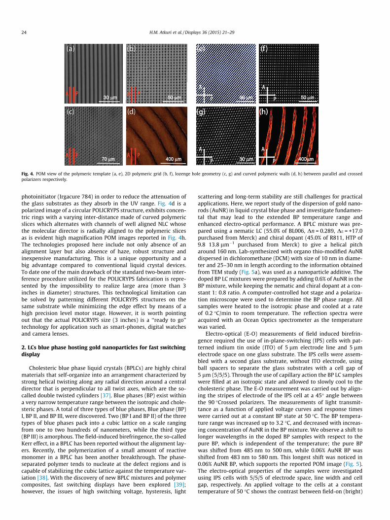
Fig. 4. POM view of the polymeric template (a, e), 2D polymeric grid (b, f), lozenge hole geometry (c, g) and curved polymeric walls (d, h) between parallel and crossedpolarizers respectively.
24 H.M. Atkuri et al. / Displays 36 (2015) 21–29
photoinitiator (Irgacure 784) in order to reduce the attenuation ofthe glass substrates as they absorb in the UV range. Fig. 4d is apolarized image of a circular POLICRYPS structure, exhibits concen-tric rings with a varying inter-distance made of curved polymericslices which alternates with channels of well aligned NLC whosethe molecular director is radially aligned to the polymeric slicesas is evident high magnification POM images reported in Fig. 4h.The technologies proposed here include not only absence of analignment layer but also absence of haze, robust structure andinexpensive manufacturing. This is a unique opportunity and abig advantage compared to conventional liquid crystal devices.To date one of the main drawback of the standard two-beam inter-ference procedure utilized for the POLICRYPS fabrication is repre-sented by the impossibility to realize large area (more than 3inches in diameter) structures. This technological limitation canbe solved by patterning different POLICRYPS structures on thesame substrate while minimizing the edge effect by means of ahigh precision level motor stage. However, it is worth pointingout that the actual POLICRYPS size (3 inches) is a ‘‘ready to go’’technology for application such as smart-phones, digital watchesand camera lenses.
2. LCs blue phase hosting gold nanoparticles for fast switchingdisplay
Cholesteric blue phase liquid crystals (BPLCs) are highly chiralmaterials that self-organize into an arrangement characterized bystrong helical twisting along any radial direction around a centraldirector that is perpendicular to all twist axes, which are the so-called double twisted cylinders [37]. Blue phases (BP) exist withina very narrow temperature range between the isotropic and chole-steric phases. A total of three types of blue phases, Blue phase (BP)I, BP II, and BP III, were discovered. Two (BP I and BP II) of the threetypes of blue phases pack into a cubic lattice on a scale rangingfrom one to two hundreds of nanometers, while the third type(BP III) is amorphous. The field-induced birefringence, the so-calledKerr effect, in a BPLC has been reported without the alignment lay-ers. Recently, the polymerization of a small amount of reactivemonomer in a BPLC has been another breakthrough. The phase-separated polymer tends to nucleate at the defect regions and iscapable of stabilizing the cubic lattice against the temperature var-iation [38]. With the discovery of new BPLC mixtures and polymercomposites, fast switching displays have been explored [39];however, the issues of high switching voltage, hysteresis, light
scattering and long-term stability are still challenges for practicalapplications. Here, we report study of the dispersion of gold nano-rods (AuNR) in liquid crystal blue phase and investigate fundamen-tal that may lead to the extended BP temperature range andenhanced electro-optical performance. A BPLC mixture was pre-pared using a nematic LC (55.0% of BL006, Dn = 0.289, De = +17.0purchased from Merck) and chiral dopant (45.0% of R811, HTP of9.8 13.8 lm�1 purchased from Merck) to give a helical pitcharound 160 nm. Lab-synthesized with organo thio-modified AuNRdispersed in dichloromethane (DCM) with size of 10 nm in diame-ter and 25–30 nm in length according to the information obtainedfrom TEM study (Fig. 5a), was used as a nanoparticle additive. Thedoped BP LC mixtures were prepared by adding 0.6% of AuNR in theBP mixture, while keeping the nematic and chiral dopant at a con-stant 1: 0.8 ratio. A computer-controlled hot stage and a polariza-tion microscope were used to determine the BP phase range. Allsamples were heated to the isotropic phase and cooled at a rateof 0.2 �C/min to room temperature. The reflection spectra wereacquired with an Ocean Optics spectrometer as the temperaturewas varied.
Electro-optical (E-O) measurements of field induced birefrin-gence required the use of in-plane-switching (IPS) cells with pat-terned indium tin oxide (ITO) of 5 lm electrode line and 5 lmelectrode space on one glass substrate. The IPS cells were assem-bled with a second glass substrate, without ITO electrode, usingball spacers to separate the glass substrates with a cell gap of5 lm (5/5/5). Through the use of capillary action the BP LC sampleswere filled at an isotropic state and allowed to slowly cool to thecholesteric phase. The E-O measurement was carried out by align-ing the stripes of electrode of the IPS cell at a 45� angle betweenthe 90 �Crossed polarizers. The measurements of light transmit-tance as a function of applied voltage curves and response timeswere carried out at a constant BP state at 50 �C. The BP tempera-ture range was increased up to 3.2 �C, and decreased with increas-ing concentration of AuNR in the BP mixture. We observe a shift tolonger wavelengths in the doped BP samples with respect to thepure BP, which is independent of the temperature; the pure BPwas shifted from 485 nm to 500 nm, while 0.06% AuNR BP wasshifted from 483 nm to 580 nm. This longest shift was noticed in0.06% AuNR BP, which supports the reported POM image (Fig. 5).The electro-optical properties of the samples were investigatedusing IPS cells with 5/5/5 of electrode space, line width and cellgap, respectively. An applied voltage to the cells at a constanttemperature of 50 �C shows the contrast between field-on (bright)

Fig. 5. (a) TEM images of organo-thio monolayer protected AuNRs in 0.0006% AuNRs in blue phase liquid crystal at 50 �C, (b) the transmittance–voltage (TV) curve of pure BPand 0.06% AuNR BP device, and (c) the POM images of (b) pure BP samples (c) 0.06% AuNR BP. The Figure is reproduced from Ref. [41]. (For interpretation of the references tocolour in this figure legend, the reader is referred to the web version of this article.)
H.M. Atkuri et al. / Displays 36 (2015) 21–29 25
and field-off (dark) states as seen in Fig. 5b. The POM images arethe manifest of the transmittance versus applied voltage curvesfor both pure and doped BPs (Fig. 5c). With AuNR doping the BPis switched to a stripe domain at a low voltage where the field isapplied in the direction normal to the stripes. The discontinuedstripes arise from imperfect electrode patterning during the sub-strate preparation. By contrast, the disappearance of the stripedomain for pure BP occurs at a higher voltage. The electro-opticalstudy shows a reduction in the threshold voltage (Vth) of the doped0.06% AuNR BP (Vth = 27.3 V) with respect to the pure BP(Vth = 34.6 V). The AuNRs doped BPLC exhibits the same light trans-mission as that of the BPLC at the field-on state at a lower voltage.One of the advantages of BPLC is its fast response time. In the mea-sured response time of the pure BPLC, the rise time was 2.1 ms andthe fall time was 1.7 ms. Conversely, in the measured responsetime for the 0.06% AuNR doped BPLC, the rise time was 15.3 msand the fall time was 5.9 ms. The response time of 0.06% AuNRdoped BPLC is slightly higher than that of the pure BPLC. This phe-nomenon can be explained by a prior report [40]. This result isbecause the rise time for the AuNRs doped sample would be slowerif the applied voltage is close to the critical voltage to unwind thecholesteric pitches (Vc). To speed up the turn on time, one shouldapply an overdrive voltage to the Kerr device. The analyses of falltimes imply that the fall time of AuNRs doped sample is abouttwice slower that of the pure BPLC. We can speculate that thiscould be due to the increase in rotational viscosity arising fromthe inclusion of AuNRs at the disclinations, which requires extraenergy for local double twists to overcome the extra exclusive vol-ume of the AuNRs [41]. In this way we have demonstrated that BPis stabilized as a result of doping AuNR. The BP temperature rangewas increased up to 3.2 �C, and decreased with increasing concen-tration of AuNR in the BP mixture. The appearance of orange and
red domains in POM images is supported by reflection spectra datashowing a shift to longer wavelengths with respect to non-dopedBP liquid crystals. It is seen that the greatest shift in the maximumwavelength occurs with 0.06% AuNR BP. This suggests that AuNRssuccessfully stabilize the BP medium and optimize thermal stabil-ity at low concentrations. In the electro-optical induced Kerr effect,the optimization in the doped AuNR BP LC device also led to areduction in threshold voltage (Vth); Vth (34.6V) of pure BP, andVth (27.3V) of the doped BP mixture.
3. Polymer stabilized liquid crystals
LCs and polymers have been developed for various electro-opti-cal applications such as light shutter, optical switch, optical lensand displays [42]. Polymer stabilized cholesteric textures (PSCTs)and polymer dispersed liquid crystals (PDLCs) technologies arewidely used in these fields. For PSCTs, cholesteric textures can bestabilized by polymer network. There are three textures (states)of cholesteric liquid crystal (Ch-LC) used in PSCTs, i.e., planar (P),focal conic (FC) and homeotropic (H) states for display and pho-tonic devices [43–46]. For normal mode PSCT, the material is opti-cal scattering and opaque at zero fields, because the LC is in the FCstate and the spatial refractive index varies between differentdomains in the zero fields. When an electric field is applied, thematerial becomes transparent since the LC is aligned in the H stateby the electric field. The refractive index of the LC and the polymerare matched in this case. For reverse mode PSCT, the LC is in the Pstate without external fields applied due to the alignment layer onthe substrate. The reflected wavelength of the P state is in theinfrared range. Therefore the material is transparent at zero field.When a proper electric field is applied, the LC is changed to the

Fig. 7. Response of a bistable CH-LC to voltage pulses. (a) Initially in the planar stateand (b) initially in the focal conic state. Reprinted with permission from[49].
�Jo
hn
Wil
eyan
dSo
ns
2006
Fig. 8. Schematic diagram of a bistable PSCT light shutter using dual frequencyliquid crystal.
26 H.M. Atkuri et al. / Displays 36 (2015) 21–29
FC state. The material becomes optical scattering and opaque. Theelectric-optical properties of normal mode and revers mode aremonostable [47], whose voltage–transmittance curved are shownin Fig. 6. We can see in the normal mode and reverse mode PSCTs,a voltage must be applied to sustain one of optical states in normalmode or reverse mode PSCTs. Later, bistable PSCT devices havebeen developed using positive Ch-LC [48]. The transmittanceresponse to a voltage pulse [49] is shown in Fig. 7. Due to an energybarrier created by a certain amount of polymer or a surface align-ing effect, both P state and FC state can be stable at zero field andbe switched by different voltage pulses. For examples, if the initialstate is FC state (scattering state), when applying a voltage pulselarge than V5 (Fig. 2), the LC texture will be switched to P state(transparent state). If the initial state is P state, when applying avoltage pulse at V2, the LC texture will be change to FC state. Novoltage has to be applied to sustain the optical states in the bista-ble PSCTs. Dual frequency LCs [50] have also been used in normalPSCT for fast response time [51] and in bistable PSCTs with P stateand FC state [52]. For a dual frequency LC (DFLC), at low frequencyelectric field, it has a positive dielectric anisotropy and the LC mol-ecules tend to align along the applied electric field and at high fre-quency electric field, the LC has a negative dielectric anisotropyand the molecules tend to align perpendicular to the applied elec-tric field. The cross-over frequency of DFLC is the frequency wherethe dielectric anisotropy is zero. The low crossover frequency ofdual frequency LC is favorite as it will be more suitable for practicalapplications. Another bistable PSCT using DFLC where the H andthe FC state are stable at zero field have been developed [53], asshown in Fig. 8. The DFLC is used to switch the shutter by a low-frequency or a high-frequency electric pulse. The Ch-LC textures(H and FC state) of the material are hold at zero field by properpolymer networks. There is no power required to sustain the opti-cal states in this system. The device is very energy-saving. Suchbistable PSCT between H state and FC state is different from theconventional bistable PSCT using P state and FC state [48]. Theproper polymer network, chiral dopant concentration and curingcondition are the key to achieve such devices. Due to higher con-centration of chiral dopant, the FC state is more scattering thanconventional bistable PSCT FC mode. The contrast ratio (CR) canbe 9.4:1 in a single-layered cell and further increased to 22.0:1 ina double-layered sample. This bistable light shutter can be usedas architectural or greenhouse windows and electric books [54].Afterwards, more PSCT or bistable PSCT were designed and studied[55–59]. The three states of CH-LC, H, P and FC are used to be stableby polymers or alignment layers. The LC materials (such as
Fig. 6. Transmittance of normal mode and reverse mode of PSCT versus the appliedvoltage. Reprinted with permission from [47].
�A
IPPu
blis
hin
gLL
C19
92
positive, negative or dual frequency LCs), polymers with differentmonomer functionalities, concentrations, curing condition (suchas UV curing time, intensity and temperature), driving methodincluding different driving voltages, frequencies or timing can beused to optimize PSCTs to get higher CR, wider viewing angleand lower driving voltage.
4. Electrofluidic technology for displays
Electrowetting is often the modification of contact angle andthus hydrophobic properties of a surface by applying varyingamounts of voltage. Next to LCD and OLED technology, the closestpossible emerging technology that has demonstrated a consider-able future potential may be electrofluidic technology. It has madeits presence clear in various aspects of an ideal display product. Ithas been demonstrated to be useful as smart windows [60–62],sunlight steering [63] displays, video speed operable [64] displays,sunlight readable and billboard [65] displays. In addition, oftenthese displays independently demonstrate quite a few of the estab-lished LCD specs such as color gamut, brightness [66], contrast justto name a few. The interest in this technology may well be consid-ered to come into limelight after the work of Hayes et al. in termsof demonstrating video speed electronic paper [64]. However,often it is difficult to meet the well-established strict display stan-dards in an integrated system that have had successfully beendemonstrated by LCDs. LCDs have their limitations includingstrictly limited operation by the deep need to use polarizers andthey are often far from a lively appeal. In other words, LCDs doesnot provide the picture and video quality that an unaltered printedcolor could provide on a printed paper. Commercializing this inter-esting electrowetting technology to a wide variety of customerbase and consumer markets may continue to be challenging, butthere are a few active and inactive spin offs that have had focused

Table 1Physical parameters of the solution (OS30/PG).
Physical property Measured value (±5% error)
IFT 110 dyne/cmSurface tension (PG-pigment) 34 dyne/cmPigment particle size in PG (D50) 50 nmConductivity (PG-pigment) 4–8 lS/cmViscosity (PG-pigment) 62 cp
Fig. 9. Various 3.5 lm electrowetting devices in operating ON (a), (b) and OFF (c)state.
H.M. Atkuri et al. / Displays 36 (2015) 21–29 27
on developing various electrowetting based displays. Some of theminclude Varioptic, Poly Vision, Gammadynamics, and LiquaVista.Often one of the biggest issues of this technology seems to bethe demanding long lifetime of the display. And such lifetimecannot be achieved without the intense research to find moreimmiscible polar and non-polar liquid combinations that provideclear and color states that could potentially withstand various
Fig. 10. Low ion ink filled electrowetting device in
weathering tests without compromising the display aestheticsover the lifetime of the display. In addition, the only successfulcompany that has successfully demonstrated a fully functionaland LCD comparable electrowetting may well be SamsungNetherlands R&D center [67]. Its success has been based on dem-onstrating electrowetting technology that is much adaptable tocurrent liquid crystal display production lines. However, their big-gest challenge and advantage may well be implementing the samefor mass production of electrowetting displays and replacingexpensive liquid crystal materials respectively. Over all we think,longevity of an electrowetting display is one of the key physicalproperties that needs more research and development. As men-tioned above, such longevity is limited by the variety of availablepolar and non-polar fluid combinations.
Here, we focus on one of such combinations. We present resultsobtained by using immiscible fluid combination of propylene gly-col (PG) based ink (pigment based color fluid) and OS30 (clearfluid). OS30 was used as non-polar clear fluid and PG is used aspolar fluid with �4% of black pigment dispersed in it. Interfacialtension (IFT), surface tension of PG-pigment/OS30 combination,particle size of pigment and other critical physical parametersare given in Table 1. As one may notice, IFT is function of pressure,temperature, and the composition of each phase. Transparent bot-tom substrate is fabricated with glass substrate and PerMX film.The film is characterized by negative working, chemicallyamplified dielectric epoxy polymer film made with three layer(polyester/microlithographic polymer/polyethylene layers). Thefilm is often suitable for structuring, bonding, plating and etchingapplications. The bottom and corresponding top substrate arecoated with 600 nm/100 nm layers of Parylene-C/Cytop layersrespectively. The cell gap of the electrowetting devices is con-trolled at 3.5 lm. The device is filled and assembled using abovementioned low-ion pigment based PG/OS30 (polar/non-polar) fluidcombination. The cell gap was well controlled and observed morethan �95% fill factor. Fig. 9a and b shows various electrowettingdevices in ON-state and Fig. 9c shows the device in OFF state.However, it is often challenging to provide a quality device thatdemonstrate long life operation of more than �100 h with no var-iation in the image quality. Figs. 10a, b and 11a, b show contrastvariation at 0, 1, 5 and 30 h operation respectively on a differentoperating segment of the device with a larger cell gap. AndFig. 11c shows contrast variation after 25 h continuous operationfrom 5 h to 30 h or it is the contrast difference between 5 h and25 h operated device. In 3 days of operation, fewer than <50% pix-els showed either full actuation or retained initial contrast. Only a
the ON state after 0:00 h (a) and 1:00 h (b).

Fig. 11. Electrowetting device in the ON state after 5:00 h (a) and 30:00 h (b). (c) Represents the contrast variation obtained after 25 h.
28 H.M. Atkuri et al. / Displays 36 (2015) 21–29
few than 25% of pixels showed both characteristics. Possibleimportant reasons for varying pixel-to-pixel contrast variation in20–30 h is unexpected and is not clearly understand. The main rea-sons for short lifetime of this combination of materials may not benon-polar fluid, PerMX layer, ITO and drive electronics. The mainissue may potentially be the quality of dielectric layer, which isParylene-C, and possible breakdown of color pigment in the polarfluid. There may be impurities as well in the pigment that mightbe causing ink breakdown. Small particle break down in the pig-ment may cause large particles in the ink and they also may causevarying degrees of phase (fast/slow) separation thus leading tocontrast changes. The quality of ITO has not been checked on thebottom and top substrates before and after device operation, butthe varying possible impurities from Paralyne C may expose PGto varying ITO lines/areas to change effective voltage experiencedby the pixels. The critical next steps may need to be understandingchemistry of polymer/PG/pigment diffusion into the non-polarfluid OS30. Or in a broader way understand the diffusion mecha-nism between polar and non-polar fluids under varying circum-stances of temperature and intense and prolonged deviceoperation.
5. Conclusion
We have reported an overview of recent advances in LCD appli-cations. Particularly, in order to eliminate the need for anymechanical alignment and rubbing process for future LCD paneldevelopment, we have proposed a ‘‘surfactant free’’ method basedon periodic structures realized through nanoimprint lithography,interference holography and polymer stabilized LCs. Further, wehave reported on the possibility to improve the optical and elec-tro-optical properties of modern LCD by combing the propertiesof LCs blue phase and nanomaterials. In particular, we haveobserved that the response time can be improved by doping a cho-lesteric liquid crystal blue phase with gold nanorods. Finally, wehave analyzed an emerging technology for further improve noveldisplays based on the modification of the wetting properties of asurface. Electrowetting technology has the capability to realizehigh quality images that ensure excellent indoor and outdoor read-ability while minimizing the battery consumption.
Acknowledgments
E.S.P. Leong and Y.J. Liu thank the funding support from JointCouncil Office (JCO) of the Agency for Science, Technology andResearch (A⁄STAR) under the Grant No. 12302FG012. G. Palermoand L. De Sio thank the funding support from the Air Force Officeof Scientific Research (AFOSR), Air Force Research Laboratory(AFRL), U.S. Air Force, under Grant FA9550-14-1-0050 (P.I. L. DeSio, EOARD 2014/2015) and the Materials and ManufacturingDirectorate, AFRL.
References
[1] P. Slikkerveer, P. Bouten, P. Cirkel, J. de Goede, H. Jagt, N. Kooyman, G. Nisato, R.van Rijswijk, P. Duineveld, A fully flexible colour display, SID Symp. Dig. Tech.Pap. 35 (2004) 770–773.
[2] S. Varghese, S. Narayanankutty, C.W.M. Bastiaansen, G.P. Crawford, D.J. Broer,Patterned alignment of liquid crystals by l-rubbing, Adv. Mater. 16 (2004)1600–1605.
[3] J. Osterman, C. Ad_as, L. Madsen, K. Skarp, Properties of azo-dye alignmentlayer on plastic substrates, SID Symp. Dig. Tech. Pap. 36 (2005) 772–775.
[4] V. Konovalov, V. Chigrinov, H.S. Kwok, H. Takada, H. Takatsu, Photoalignedvertical aligned nematic mode in liquid crystals, Japan J. Appl. Phys. 43 (2004)261–266.
[5] W. Gibbons, P. Shannon, S.T. Sun, B. Swetlin, Surface-mediated alignment ofnematic liquid crystals with polarized laser light, Nature 351 (1991) 49–50.
[6] D. Andrienko, Y. Kurioz, Y. Reznikov, C. Rosenblatt, R. Petschek, O.Lavrentovich, D. Subacius, Tilted photo-alignment of a nematic liquid crystalinduced by a magnetic field, J. Appl. Phys. 83 (1998) 50–55.
[7] J.K. Kim, C.J. Choi, J.S. Park, S.J. Jo, B.H. Hwang, M.K. Jo, D. Kang, S.J. Lee, Y.S. Kim,H.K. Baik, Orientational transition of liquid crystal molecules by aphotoinduced transformation process into a recovery free silicon oxide layer,Adv. Mater. 20 (2008) 3073–3078.
[8] P. Chaudhari, J. Lacey, S.A. Lien, J. Speidell, Atomic beam alignment of liquidcrystal, Japan J. Appl. Phys. 37 (1998) L55–L56.
[9] P. Chaudhari, J. Lacey, J. Doyle, E. Galligan, S.-C.A. Lien, A. Callegari, G.Hougham, N.D. Lang, P.S. Andry, R. John, K.-H. Yang, M. Lu, C. Cai, J. Speidell, S.Purushothaman, J. Ritsko, M. Samant, J. Stöhr, Y. Nakagawa, Y. Katoh, Y. Saitoh,K. Sakai, H. Satoh, S. Odahara, H. Nakano, J. Nakagaki, Y. Shiota, Atomic-beamalignment of inorganic materials for liquid crystal displays, Nature 411 (2001)56–59.
[10] L. Janning, Thin film surface orientation for liquid crystal, Appl. Phys. Lett. 21(1972) 173.
[11] K.C. Kim, H.J. Ahn, J.B. Kim, B.H. Hwang, H.K. Baik, Novel alignment mechanismof liquid crystal on a hydrogenated amorphous silicon oxide, Langmuir 21(2005) 11079–11084.
[12] D.W. Berreman, Solid surface shape and the alignment of an adjacent nematicliquid crystal, Phys. Rev. Lett. 28 (1972) 1683–1684.
[13] D.W. Berreman, Alignment of liquid crystals by grooved surfaces, Mol. Cryst.Liq. Cryst. 23 (1973) 215–231.
[14] Y.J. Liu, W.W. Loh, E.S.P. Leong, T.S. Kustandi, X.W. Sun, J.H. Teng,Nanoimprinted ultrafine line and space nanogratings for liquid crystalalignment, Nanotechnology 23 (2012) 465302–465307.
[15] S.Y. Chou, P.R. Krauss, P.J. Renstrom, Nanoimprint lithography, J. Vac. Sci.Technol., B 14 (1996) 4129–4133.
[16] M.D. Austin, H. Ge, W. Wu, M. Li, Z. Yu, D. Wasserman, S.A. Lyon, S.Y. Chou,Fabrication of 5 nm linewidth and 14 nm pitch features by nanoimprintlithography, Appl. Phys. Lett. 84 (2004) 5299–5301.
[17] L.J. Guo, Nanoimprint lithography: methods and material requirements, Adv.Mater. 19 (2007) 495–513.
[18] S.Y. Yew, T.S. Kustandi, H.Y. Low, J.H. Teng, Y.J. Liu, E.S.P. Leong, Single-material-based multilayered nanostructures fabrication via reverse thermalnanoimprinting, Microelectron. Eng. 88 (2011) 2946–2950.
[19] E.S.P. Leong, S.Y. Yew, T.S. Kustandi, Y.J. Liu, H. Tanoto, Q.Y. Wu, W.W. Loh, S.L.Teo, J.H. Teng, New approach for multilayered microstructures fabricationbased on a water-soluble backing substrate, ACS Appl. Mater. Interfaces 5(2013) 5898–5902.
[20] E.S.P. Leong, S.J. Wu, N. Zhang, W.W. Loh, E.H. Khoo, G.Y. Si, H.T. Dai, Y.J. Liu,Optical properties of ultrafine line and space polymeric nanogratings coatedwith metal and metal-dielectric-metal thin films, Nanotechnology 25 (2014)055203–055208.
[21] H.-R. Kim, J.-W. Jung, Y.-J. Lee, J.-H. Kim, Liquid crystal alignment with amolecular template of imprinted polymer layer during phase separation, Appl.Phys. Lett. 88 (2006). 113504-3.
[22] J.S. Gwag, M. Oh-e, M. Yoneya, H. Yokoyama, H. Satou, S. Itami, Advancednanoimprint lithography using a graded functional imprinting materialtailored for liquid crystal alignment, J. Appl. Phys. 102 (2007). 063501-3.
[23] Y. Yi, M. Nakata, A.R. Martin, N.A. Clark, Alignment of liquid crystals bytopographically patterned polymer films prepared by nanoimprintlithography, Appl. Phys. Lett. 90 (2007). 163510-3.

H.M. Atkuri et al. / Displays 36 (2015) 21–29 29
[24] R.S. Lin, J.A. Rogers, Molecular-scale soft imprint lithography for alignmentlayers in liquid crystal devices, Nano Lett. 7 (2007) 1613–1621.
[25] H.-G. Park, J.-J. Lee, K.-Y. Dong, B.-Y. Oh, Y.-H. Kim, H.-Y. Jeong, B.-K. Ju, D.-S.Seo, Homeotropic alignment of liquid crystals on a nano-patterned polyimidesurface using nanoimprint lithography, Soft Matter 7 (2011) 5610–5614.
[26] H. Takahashi, T. Sakamoto, H. Okada, Liquid crystal device with 50 nmnanogroove structure fabricated by nanoimprint lithography, J. Appl. Phys. 108(2010). 113529-3.
[27] N. Ishizawa, K. Idei, T. Kimura, D. Noda, T. Hattori, Resin micromachining byroller hot embossing, Microsyst. Technol. 14 (2008) 1381–1388.
[28] C.J. Ting, F.Y. Chang, C.F. Chen, C.P. Chou, Fabrication of an antireflectivepolymer optical film with subwavelength structures using a roll-to-roll micro-replication process, J. Micromech. Microeng. 18 (2008). 075001-6.
[29] S.H. Ahn, L.J. Guo, Large-area roll-to-roll and roll-to-plate nanoimprintlithography: a step toward high-throughput application of continuousnanoimprinting, ACS Nano 3 (2009) 2304–2310.
[30] R. Caputo, L. De Sio, A. Veltri, C. Umeton, A.V. Sukhov, Development of a newkind of switchable holographic grating made of liquid-crystal films separatedby slices of polymeric material, Opt. Lett. 29 (2004) 1261–1263.
[31] L. De Sio, A. Veltri, A. Tedesco, R. Caputo, C. Umeton, A.V. Sukhov,Characterization of an active control system for holographic setupstabilization, Appl. Opt. 47 (2008) 1363–1367.
[32] L. De Sio, S. Serak, N. Tabiryan, C. Umeton, Mesogenic versus non-mesogenicazo dye confined in a soft-matter template for realization of opticallyswitchable diffraction gratings, J. Mater. Chem. 21 (2011) 6811–6814.
[33] L. De Sio, S. Ferjani, G. Strangi, C. Umeton, R. Bartolino, Soft periodicmicrostructures containing liquid crystals, J. Phys. Chem. B 117 (2013)1176–1185.
[34] L. De Sio, S. Ferjani, G. Strangi, C. Umeton, R. Bartolino, Universal soft mattertemplate for photonic applications, Soft Matter 7 (2011) 3739–3743.
[35] L. De Sio, P. D’Aquila, E. Brunelli, G. Strangi, D. Bellizzi, G. Passarino, C.P.Umeton, R. Bartolino, Directed organization of DNA filaments in a soft mattertemplate, Langmuir 29 (2013) 3398–3403.
[36] L. De Sio, N. Tabiryan, T. Bunning, Spontaneous radial liquid crystals alignmenton curved polymeric surfaces, Appl. Phys. Lett. 104 (2014). 221112-4.
[37] D.C. Wright, N.D. Mermin, Crystalline liquids: the blue phases, Rev. Mod. Phys.61 (1989) 385–432.
[38] H. Kikuchi, M. Yokota, Y. Hisakado, H. Yang, T. Kajiyama, Polymer-stabilizedliquid crystal blue phases, Nat. Mater. 1 (2002) 64–68.
[39] J. Yan, S.T. Wu, Polymer-stabilized blue phase liquid crystals: a tutorial, Opt.Mater. Exp. 1 (2011) 1527–1535.
[40] H. Choi, H. Higuchi, H. Kikuchi, Electro-optic response of liquid crystalline bluephases with different chiral pitches, Soft Matter 7 (2011) 4252–4256.
[41] J.-M. Wong, J.-Y. Hwang, L.-C. Chien, Electrically reconfigurable and thermallysensitive optical properties of gold nanorods dispersed liquid crystal bluephase, Soft Matter 7 (2011) 7956–7959.
[42] S.-T. Wu, D.-K. Yang, Reflective Liquid Crystal Displays, John Wiley & Sons Inc.,New York, 2001.
[43] H. Ren, S.-T. Wu, Reflective reversed-mode polymer stabilized cholesterictexture light switches, J. Appl. Phys. 92 (2002) 797–800.
[44] J. Ma, L. Xuan, Towards nanoscale molecular switch-based liquid crystaldisplays, Displays 34 (2013) 293–300.
[45] W.-L. Hsu, J. Ma, M. Graham, K. Balakrishnan, S. pau, Patterned cholestericliquid crystal polymer film, J. Opt. Soc. Am. A 30 (2013) 252–258.
[46] R. Wu, Y. Li, J. Wu, J. Ma, Q. Dai, A study of lasing wavelength by DOS in thetemperature-tunable cholesteric liquid crystal lasers, Opt. Commun. 300(2013) 1–4.
[47] D.-K. Yang, L.-C. Chien, J.W. Doane, Cholesteric liquid crystal/polymerdispersion for haze free light shutters, Appl. Phys. Lett. 60 (1992) 3102–3104.
[48] D.-K. Yang, X.-Y. Huang, Y.-M. Zhu, Bistable cholesteric reflective displays:materials and drive schemes, Annu. Rev. Mater. Sci. 27 (1997) 117–146.
[49] D.-K. Yang, S.-T. Wu, Fundamentals of Liquid Crystal Devices, John Wiley &Sons Inc., New York, 2006.
[50] H. Xianyu, S.-T. Wu, C.-L. Lin, Dual frequency liquid crystals: a review, Liq.Cryst. 36 (2009) 717–726.
[51] M. Xu, D.-K. Yang, Dual frequency cholesteric light shutters, Appl. Phys. Lett.70 (1997) 720–722.
[52] M. Xu, D.-K. Yang, Electrooptical properties of dual-frequency cholestericliquid crystal reflective display and drive scheme, Jpn. J. Appl. Phys. 38 (1999)6827–6830.
[53] J. Ma, L. Shi, D.-K. Yang, Bistable polymer stabilized cholesteric texture lightshutter, Appl. Phys. Exp. 3 (2010) 021702.
[54] D.K. Yang, Review of operating principle and performance of polarizer-freereflective liquid-crystal displays, J. SID 16 (2008) 117–124.
[55] Y.-C. Hsiao, C.-Y. Tang, W. Lee, Fast-switching bistable cholesteric intensitymodulator, Opt. Express 19 (2011) 9744–9749.
[56] H.-H. Liang, C.-C. Wu, P.-H. Wang, J.-Y. Lee, Electro-thermal switchable bistablereverse mode polymer stabilized cholesteric texture light shutter, Opt. Mater.33 (2011) 1195–1202.
[57] Y.-C. Hsiao, C.-T. Hou, V.Y. Zyryanov, W. Lee, Multichannel photonic devicesbased on tristable polymer-stabilized cholesteric textures, Opt. Express 19(2011) 23952–23957.
[58] P. Kumar, S.-W. Kang, S.H. Lee, Advanced bistable cholesteric light shutter withdual frequency nematic liquid crystal, Opt. Mater. Exp. 2 (2012) 1121–1134.
[59] K.-H. Kim, B.-H. Yu, S.-W. Choi, S.-W. Oh, T.-H. Yoon, Dual mode switching ofcholesteric liquid crystal device with three-terminal electrode structure, Opt.Express 20 (2012) 24376–24381.
[60] H. You, A.J. Steckl, Versatile electrowetting arrays for smart windowapplications-from small to large pixels on fixed and flexible substrates, Sol.Energy. Mat. Sol. Cells 117 (2013) 544–548.
[61] S.W. Kuo, K.L. Lo, W.Y. Cheng, H.H. Lee, Y.H. Tsai, Y.S. Ku, P.P. Cheng, P.-J. Su,J.W. Shiu, A novel electrowetting-based display for future smart windowapplication, SID Symp. Dig. Tech. Pap. 42 (2011) 232–235.
[62] Unpublished Gammadynamics R&D Work by Hari Atkuri/Ken Dean/JasonHeikenfeld.
[63] J. Cheng, S. Park, C.L. Chen, Optofluidic solar concentrators usingelectrowetting tracking: concept, design, and characterization, Sol. Energy 89(2013) 152–161.
[64] R.A. Hayes, B.J. Feenstra, Video-speed electronic paper based onelectrowetting, Nature 425 (2003) 383–385.
[65] K. Blankenbach, M. Jentsch, J. Rawert, D. Jerosch, A. Bitman, F. Bartels, Sunlightreadable bistable electrowetting displays for indicators and billboards, SIDSymp. Dig. Tech. Pap. 42 (2011) 1527–1530.
[66] J. Heikenfeld, M. Hagedon, A. Russell, S. Yang, E. Kreit, K. Zhou, S. Smith, H.Atkuri, L. Salem, K. Dean, J. Rudolph, A high-brightness electrofluidic displayfilm, SID Symp. Dig. Tech. Pap. 43 (2012) 75–78.
[67] http://www.samsung.com/global/business/semiconductor/aboutus/business/openinnovation/operation-overseas-research-centers.