Embed Size (px)
Citation preview
Ultramicroscopy 49 (1993) 26-36 laJ igrwcm~l*~taol~ '~n,m North-Holland
Development and applications of a 300 keV ultrahigh-vacuum high-resolution electron microscope
David J. Smith, M. Gajdardziska-Jos i fovska , Ping Lu ~, M.R. McCar tney , J. Podbrdsky 2 Center for Solid State Science and Department of Physics, Arizona State Uniz'ersity, Tempe. AZ 85287, USA
P.R. Swarm and J.S. Jones Gatan Inc., 6678 Owens Drit:e, Pleasanton, CA 94566, USA
Received 27 July 1992; at Editorial Office 31 August 1992
Dedicated to Elmar Zeitler on the occasion of his 65th birthday
A commercial 300 keV high-resolution electron microscope has been modified for ultrahigh-vacuum operation by the provision of a novel specimen chamber, additional treatment- and cryochambers and extra pumping capacity. Measured vacuum levels after bakeout cycles are in the mid to low 10 -9 Torr range. The side-entry-type specimen holder incorporates a flexible bellows connection to minimize vibrations and thermal drift problems. The interpretable resolution of the microscope of 0.20 nm has been retained after completion of the UHV conversion, and the microscope has subsequently been used in the profile imaging and reflection microscopy geometries to study a variety of semiconductor, oxide and metal surfaces and surface reactions. These include the 7 x 7 Si{lll} and 1 × 1 GaP(II0) surface reconstructions, and phase transitions between 2 × 1 and 3 × 1 reconstructions of the CdTe(100) surface. The effects of electron irradiation, and also annealing, on MgO and rutile surfaces have been documented.
1. Introduction
Unlike conventional surface-science tech- niques which provide information averaged over extensive areas, the electron microscope, like the scanning tunneling microscope, offers the possi- bility of characterizing surface topography on a highly localized scale. The high-resolution elec- tron microscope (HREM) is nowadays capable of resolving details at the atomic level: the addition of ultrahigh-vacuum (UHV) and specimen-pre- paration capabilities to the HREM thus makes a
1 Present address: Depar tment of Mechanics and Materials Science, Rutgers University, Piscataway, NJ 08855, USA.
2 Present address: Insti tute of Scientific Ins t ruments , Czechoslovak Academy of Sciences, 612 64 Brno, Kralovo- polska 147, Czechoslovakia.
potentially powerful instrument for studying sur- faces, particularly surface reactions, provided that the surfaces of interest have first been properly cleaned. Several groups of microscopists have therefore recently been motivated either to make extensive modifications to existing HREMs [1,2] or else to incorporate major design changes into the construction of new instruments [3-7].
The approach we have adopted has been to modify a Philips 430ST HREM by providing an entirely new specimen chamber and sample holder, together with an ancillary prepara t ion/ treatment chamber, all of which can be pumped to, and be maintained at, UHV vacuum [2,8]. The specimen holder and stage were designed to al- low the specimen to be heated in situ to a tem- perature of 1200°C. The additional side-chamber enables further treatments of the sample surface,
0304-3991/93/$06.00 © 1993 - Elsevier Science Publishers B.V. All rights reserved
D.J. Smith et al. / Development and applications of a 300 keV UHV HREM 27
such as annealing, ion-milling or evaporation, to be carried out without exposure to atmosphere. Overall, the modifications have permit ted the 0.20 nm interpretable resolution of the microscope to be maintained.
We begin by summarizing some of the novel features of the modified holder, stage and cham- ber. We then describe the wide range of surface studies that have been undertaken with the in- strument. These include observations of oxides, metals and semiconductors, some of which in- volved surface reactions and electron-stimulated desorption processes at elevated temperatures. A more detailed technical description of the modifi- cations can be found elsewhere [8].
2. Description of microscope
addition of valves and modifications of the micro- scope vacuum controls. A front view of the micro- scope after installation of the U H V attachments is shown in fig. 1.
2.2. U H V uacuum
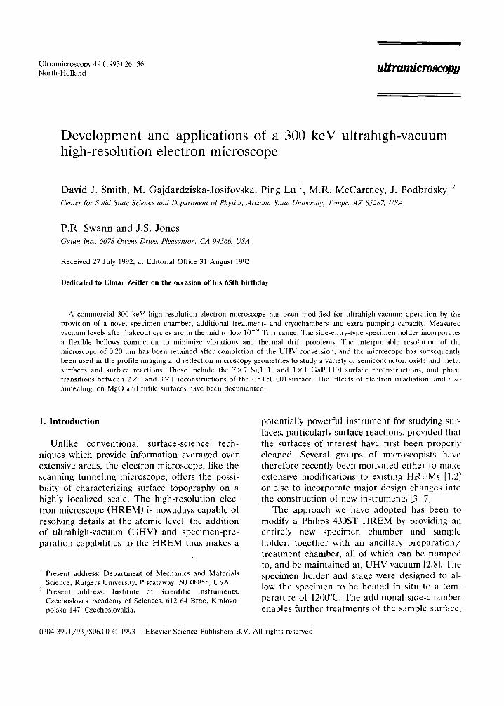
A schematic diagram of the new specimen chamber, with its additional cryo- and reaction chambers, is shown in fig. 2. This chamber repre- sents a major departure from the standard cham- ber in that it includes only metal seals, with bellows to eliminate the need for sliding O-ring seals. The two 20 g / s ion pumps, as well as the cryofingers, provide for clean pumping of the sample region. Two additional 45 g/s ion pumps are attached to the reaction and cryochambers.
2.1. Basic layout
The Philips 430ST H R E M is designed to oper- ate over the voltage range 100-300 keV. Its im- portant aberration figures are C~ = 1.0 mm and C c = 1.4 mm: its structural resolution should thus be 0.20 nm. Throughout the design, development and commissioning of the U H V modifications, we were always concerned that its performance should be maintained even though this require- ment placed difficult constraints on the overall design because the existing objective lens pole- piece gap was only 5.4 ram. The microscope is equipped with an LaB 6 electron gun and a modi- fied intermediate lens that allow a maximum electron-optical magnification to the photo- graphic negative of 900000 × . A Gatan 626 TV camera and pickup system is attached to the base of the viewing chamber for real-time image view- ing, as well as permitting videotape recording of dynamic events.
The major change to the microscope involved complete replacement of the standard specimen chamber, stage and holder, with a new UHV- compatible assembly, made primarily from stain- less steel. A cryochamber and a specimen-treat- m e n t / p r e p a r a t i o n chamber were added to the U H V section of the microscope. Extra pumping was provided for all three sections, including the
Fig. 1. Front view of the Philips-Gatan 430ST high-resolution electron microscope, as modified for ultrahigh-vacuum opera- tion, showing the modified specimen chamber, with specimen loading device and reaction chamber attached at left, and the
cryochamber at right.
28 D.J. Smith et al. / Det,eloprnent and applications o f a 300 keV UtIV HREM
Initial evacuation of the chamber when required is achieved with a turbomolecular pump, attached to the reaction chamber, which is normally switched off during microscopy sessions. The vac- uum is monitored by a residual-gas analyser and two ion gauges, although the gauge at the rear of the specimen chamber is usually also turned off during high-resolution imaging because its close proximity to the specimen stage results in image drift. The entire chamber is normally baked to a temperature of ~ 120°C, and vacuum levels through the chamber after 36 h bakeout cycles are typically in the range of (2-5) × 10 - 9 Torr.
Gate valves of novel design were developed for the specimen loadlock and the reaction chamber to minimize the overall length of the specimen loadlock mechanism. The outer valve enables ul- trahigh vacuum to be maintained within the reac- tion chamber during exchange of specimens, and the inner one makes it possible to remove the specimen holder to the reaction chamber for treatments that would otherwise compromise the vacuum in the specimen-stage region. The speci-
men holder can be rotated by a maximum angle of 15 ° when it is in the column, but it can be rotated through a complete 360 ° when it is re- tracted into the reaction chamber, thereby pro- viding greatest flexibility for access to any special surface treatments such as precision ion-milling or evaporation. The turbomolecular pump is also used for pre-pumping of the loadlock and for pumping of the reaction chamber during special gas-handling processes. Six ports are provided around the periphery of the reaction chamber for special at tachments such as evaporators, ion-guns and gas-inlet valves.
The Dewar of the cryochamber is pumped by a separate turbomolecular pump. It has two cooling reservoirs: the inner Dewar, connected to the cryofinger assembly by a flexible ribbon conduc- tor, has been designed to hold liquid helium; the outer cryoshield holds liquid nitrogen and serves to minimize heat losses. We have yet to verify that any advantage accrues from going to liquid- helium temperature, and in typical operations, both reservoirs are filled with liquid nitrogen.
I
ROUGHING LINE ~ A I R L O ~
DIFFERENTIALLY PUMPED I LH.!.o.uJ-J_.uN r ~ SPEEC'MEENN'DNSDEoRJ '°N I ~uM" ~ " h ~ l__J
TILT DRIVE k, Jl /
I I ?-t '
T Ti SUBLIMATION ION / k,~ - -
PUMP 8001/s GUN V3
t,x
... SPECIMEN LOADING REACTION SPECIMEN CRYO DEVICE I r'CHAMBER -I F--- CHAMBER ---7 I CHAMBER I
RESIDUAL GAS ANALYSER
/ " / ION GAUGE LIQUID He CRYOSTAT r--- I x,y,z TRANSLATABLE
I ..I I1( ~ ~11 I TRIODE ION) . ~ ~ % , / ~ _ _ j ~ ~ PUMP 451/s ~
I ~ L ~ J uE;,rZdraivel~e r
XYZ = STAGE DRIVES xTz = APERTURE DRIVES GATE VALVE EVAPORATOR EVAPORATOR v 1 2
Fig. 2. Schematic drawing of the overall layout for the U H V specimen chamber, also showing the additional cryo- and reaction chambers, pumping facilities, and the specimen loadlock system.
D.J. Smith et al. / DeL, elopment and applications of a 300 keV UHV HREM 29
The cryofinger assembly has two blades, one above the specimen and another below. The lat- ter has a set of three holes that act as objective apertures, and a larger open hole is used for locating the beam and for low-magnification view- ing of the sample if required. Thermally insulated micrometer drives provide accurate translation of the aperture assembly. No deterioration of high- resolution performance has been noticed due to vibrations of the cryofingers a n d / o r refrigerants during operation.
2.3. Specimen holder and stage
The specimen holder and stage of the HREM are among its most critical components. In our case, the severely confined space between the objective lens polepieces had to incorporate the cryofinger blades as well as the specimen holder. The latter should provide non-interactive x, y and z motion for the specimen, with minimal hysteresis and backlash for precise location, and also allow for a reasonable range of specimen tilting while the sample is being heated to beyond 1000°C. Special attention had to be given to the choice of the stage materials to minimize antici- pated mechanical problems, including possible sensitivity to vibration. Orthogonal hinges and jewelled pivots were utilized for the translation
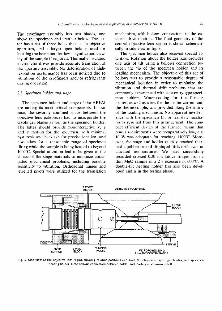
mechanism, with bellows connections to the ex- ternal drive motions. The final geometry of the central objective lens region is shown schemati- cally in side view in fig. 3.
The specimen holder also received special at- tention. Rotation about the holder axis provides one axis of tilt using a bellows connection be- tween the tip of the specimen holder and its loading mechanism. The objective of this set of bellows was to provide a reasonable degree of mechanical isolation in order to minimize the vibration and thermal drift problems that are commonly experienced with side-entry-type speci- men holders. Water-cooling for the furnace heater, as well as wires for the heater current and the thermocouple, was provided along the inside of the loading mechanism. No apparent interfer- ence with the specimen tilt or translate mecha- nisms resulted from this arrangement. The com- pact efficient design of the furnace meant that power requirements were comparatively low, e.g. 10 W was adequate for reaching ll00°C. More- over, the stage and holder quickly reached ther- mal equilibrium and displayed little drift even at elevated temperatures. We have successfully recorded crossed 0.20 nm lattice fringes from a thin MgO sample in a 2 s exposure at 600°C. A double-tilt heating holder has also been devel- oped and is in the testing phase.
Z PIVOT BLOCK OBJECTIVE POLEPEICE
FIXED Z PIVOT PUMPING SUPPORT BLOCK HOLES MICROPOSITIONING
L He ANTICONTAMINATOR
Y PIVOT BLOCK
LIVE [
Fig. 3. Side view of the objective lens region showing relative positions and sizes of polepieces, cryofinger blades, and specimen heating holder. Note bellows connection between holder and loading mechanism at left.
30 D.J. Smith et al. / Det,elopment and applications of a 300 keV UHV HREM
3. Experimental results
3.1. Evaluation of performance
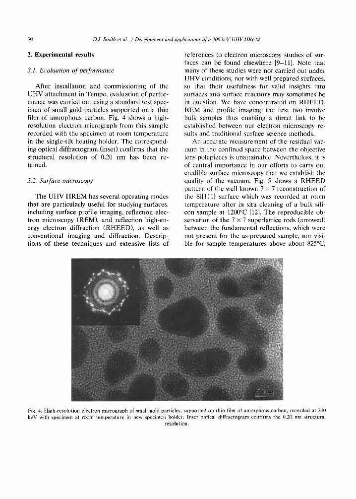
After installation and commissioning of the UHV attachment in Tempe, evaluation of perfor- mance was carried out using a standard test spec- imen of small gold particles supported on a thin film of amorphous carbon. Fig. 4 shows a high- resolution electron micrograph from this sample recorded with the specimen at room temperature in the single-tilt heating holder. The correspond- ing optical diffractogram (inset) confirms that the structural resolution of 0.20 nm has been re- tained.
3.2. Surface microscopy
The U H V H R E M has several operating modes that are particularly useful for studying surfaces, including surface profile imaging, reflection elec- tron microscopy (REM), and reflection high-en- ergy electron diffraction (RHEED) , as well as conventional imaging and diffraction. Descrip- tions of these techniques and extensive lists of
references to electron microscopy studies of sur- faces can be found elsewhere [9-11]. Note that many of these studies were not carried out under U H V conditions, nor with well prepared surfaces, so that their usefulness for valid insights into surfaces and surface reactions may sometimes be in question. We have concentrated on RHEED, REM and profile imaging: the first two involve bulk samples thus enabling a direct link to be established between our electron microscopy re- suits and traditional surface science methods.
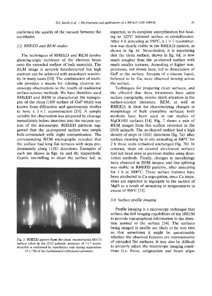
An accurate measurement of the residual vac- uum in the confined space between the objective lens polepieces is unattainable. Nevertheless, it is of central importance in our efforts to carry out credible surface microscopy that we establish the quality of the vacuum. Fig. 5 shows a R H E E D pattern of the well known 7 x 7 reconstruction of the Si{lll} surface which was recorded at room temperature after in situ cleaning of a bulk sili- con sample at 1200°C [12]. The reproducible ob- servation of the 7 × 7 superlattice rods (arrowed) between the fundamental reflections, which were not present for the as-prepared sample, nor visi- ble for sample temperatures above about 825°C,
Fig. 4. High-resolution electron micrograph of small gold particles, supported on thin film of amorphous carbon, recorded at 300 keV with specimen at room temperature in new specimen holder. Inset optical diffractogram confirms the 0.20 nm structural
resolution.
D.J. Smith et al. / Deeelopment and applications of a 300 keV UHV HREM 31
confirmed the quality of the vacuum between the cryoblades.
3.3. RHEED and REM studies
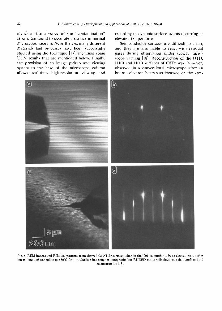
The techniques of R H E E D and REM involve glancing-angle incidence of the electron beam onto the extended surface of bulk materials. The REM image is severely foreshortened but high contrast can be achieved with monolayer sensitiv- ity in many cases [10]. The combination of meth- ods provides a means for relating electron mi- croscopy observations to the results of traditional surface-science methods. We have therefore used R H E E D and REM to characterize the topogra- phy of the clean (110) surface of GaP which was known from diffraction and spectroscopy studies to have a 1 x 1 reconstruction [13]. A sample suitable for observation was prepared by cleavage immediately before insertion into the vacuum sys- tem of the microscope. R H E E D patterns sug- gested that the as-prepared surface was simply bulk-terminated with slight contamination. The corresponding REM micrographs revealed that the surface had long fiat terraces with steps pre- dominantly along (110) directions. Examples of each are shown in figs. 6a and 6b, respectively. Gentle ion-milling to clean the surface led, as
expected, to its complete amorphization but heat- ing to 325°C initiated surface re-crystallization. After 4 h annealing at 550°C, a 1 × 1 reconstruc- tion was clearly visible in the RH EED pattern, as shown in fig. 6c. Nevertheless, it is interesting that the clean surface, shown in fig. 6d, is now much rougher than the as-cleaved surface with much smaller terraces. Annealing at higher tem- peratures, not shown here, led to dissociation of GaP at the surface. Streams of a viscous liquid, believed to be Ga, were observed moving across the surface.
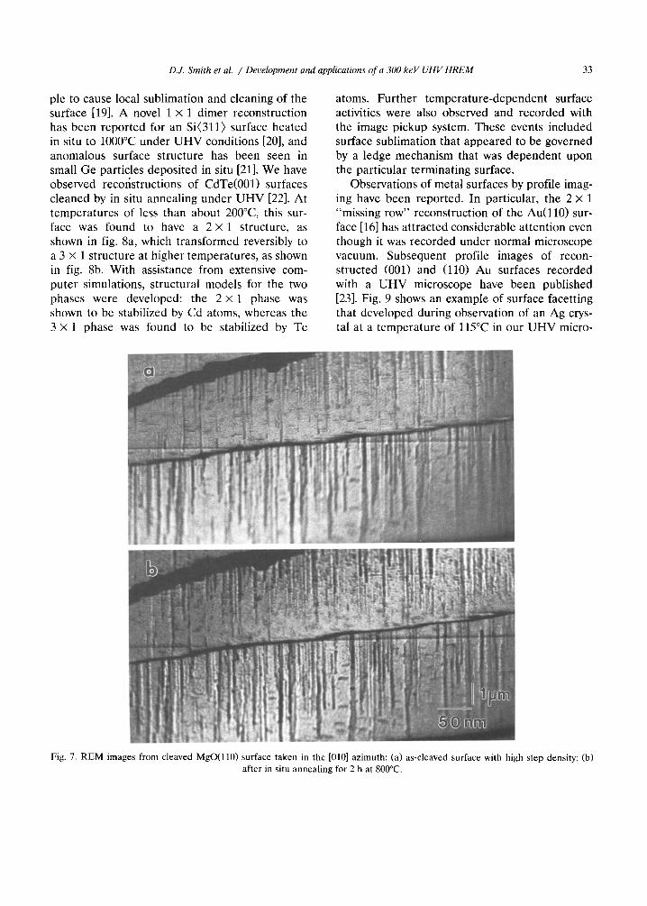
Techniques for preparing clean surfaces, and the effect(s) that these treatments have upon surface topography, receive much attention in the surface-science literature. REM, as well as RHEED, is ideal for characterizing changes in morphology of bulk crystalline surfaces: both methods have been used in our studies of MgO(100) surfaces [14]. Fig. 7 shows a pair of REM images from this surface recorded in the [010] azimuth. The as-cleaved surface had a high density of steps in (010) directions (fig. 7a): after surface cleaning by in situ annealing at 800°C for 2 h these steps remained unchanged (fig. 7b). In contrast, steps on cleaned air-cleaved surfaces had not been seen in previous studies using deco- ration methods. Finally, changes in morphology were observed in REM images, and line splitting was visible in R H E E D patterns, after annealing for 1 h at 1000°C. These surface features have been attributed to Ca segregation, since Ca impu- rities are expected to segregate to the surface of MgO as a result of annealing at temperatures in excess of 950°C [15].
3. 4. Surface profile imaging
Fig. 5. RHEED pattern from the clean, reconstructed Si{lll} surface taken in the [2111 azimuth: presence of 7;<7 recon- struction is confirmed by superlattice rods having separations
of 1/7th of the fundamental reflections (arrowed).
Profile imaging is a microscopy technique that utilizes the full imaging capabilities of the HREM to provide topographical information in the direc- tion normal to the surface [16]. The surfaces being imaged in profile are likely to be very thin so that sometimes it might be questionable whether the observed features are representative of extended flat surfaces. It may also be difficult to properly adjust the microscope imaging condi- tions (i.e. focus, astigmatism and beam align-
32 D.J. Smith et al. / Deuelopment and applications of a 300 keV UHV HREM
ment) in the absence of the "contaminat ion" layer often found to decorate a surface in normal microscope vacuum. Nevertheless, many different materials and processes have been successfully studied using the technique [17], including some UHV results that are mentioned below. Finally, the provision of an image pickup and viewing system to the base of the microscope column allows real-time high-resolution viewing and
recording of dynamic surface events occurring at elevated temperatures.
Semiconductor surfaces are difficult to clean, and they are also liable to react with residual gases during observation under typical micro- scope vacuum [18]. Reconstruction of the (111), (110) and (100) surfaces of CdTe was, however, observed in a conventional microscope after an intense electron beam was focussed on the sam-
i
Fig. 6. REM images and RHEED patterns from cleaved GaP(l l0) surface, taken in the [001] azimuth: (a, b) as-cleaved; (c, d) after ion-milling and annealing at 550°C for 4 h. Surface has rougher topography but RHEED pattern displays rods that confirm 1 x 1
reconstruction [13].
D.J. Smith et al. / Det,elopment and applications of a 300 keV UHV HREM 33
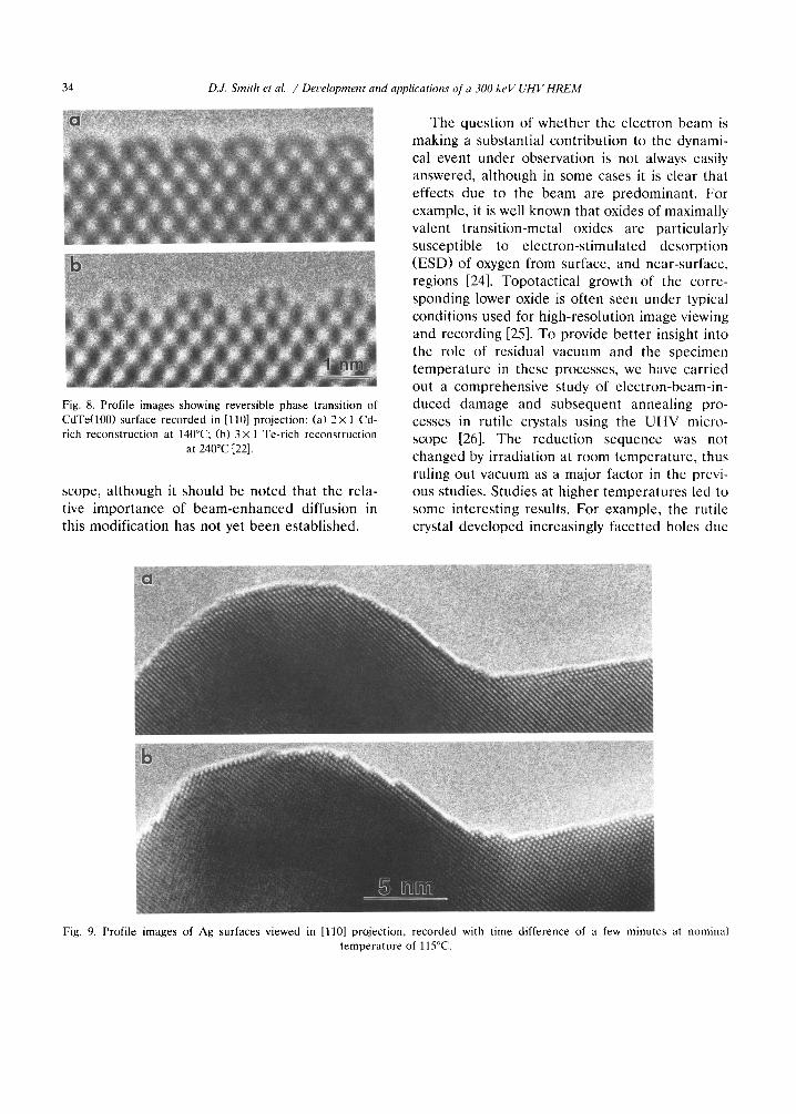
pie to cause local sublimation and cleaning of the surface [19]. A novel 1 x 1 dimer reconstruction has been reported for an Si(311) surface heated in situ to 1000°C under U H V conditions [20], and anomalous surface structure has been seen in small Ge particles deposited in situ [21]. We have observed recoristructions of CdTe(001) surfaces cleaned by in situ annealing under U H V [22]. At temperatures of less than about 200°C, this sur- face was found to have a 2 × 1 structure, as shown in fig. 8a, which transformed reversibly to a 3 × 1 structure at higher temperatures, as shown in fig. 8b. With assistance from extensive com- puter simulations, structural models for the two phases were developed: the 2 × 1 phase was shown to be stabilized by Cd atoms, whereas the 3 × 1 phase was found to be stabilized by Te
atoms. Further temperature-dependent surface activities were also observed and recorded with the image pickup system. These events included surface sublimation that appeared to be governed by a ledge mechanism that was dependent upon the particular terminating surface.
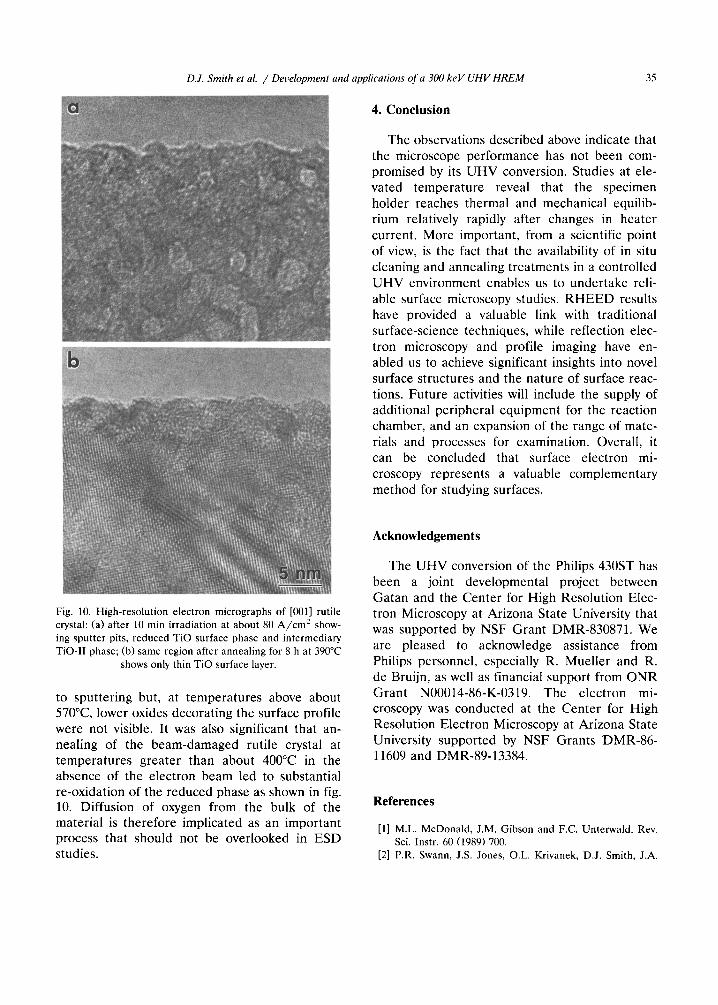
Observations of metal surfaces by profile imag- ing have been reported. In particular, the 2 × 1 "missing row" reconstruction of the Au( l l0 ) sur- face [16] has attracted considerable attention even though it was recorded under normal microscope vacuum. Subsequent profile images of recon- structed (001) and (110) Au surfaces recorded with a U H V microscope have been published [23]. Fig. 9 shows an example of surface facetting that developed during observation of an Ag crys- tal at a temperature of 115°C in our U H V micro-
Fig. 7. REM images from cleaved MgO(ll0) surface taken in the [010] azimuth: (a) as-cleaved surface with high step density; (b) after in situ annealing for 2 h at 800°C.
34 D.J. Smith et aL / Det,elopment and applications q[ a 300 keV UHV HREM
iil ,~;~'~ , ~ ~ i ~ " ~ ~ ~ , ~ ~ ' %~'i ~ )>.~ ~ ~,if ~ ~!.7 ...... ~ ' ~!'~
Fig. 8. Profile images showing reversible phase transition of CdTe(100) surface recorded in [110] projection: (a) 2 x 1 Cd- rich reconstruction at 140°C; (b) 3 × 1 Te-rich reconstruction
at 240°C [22].
scope, although it should be noted that the rela- tive importance of beam-enhanced diffusion in this modification has not yet been established.
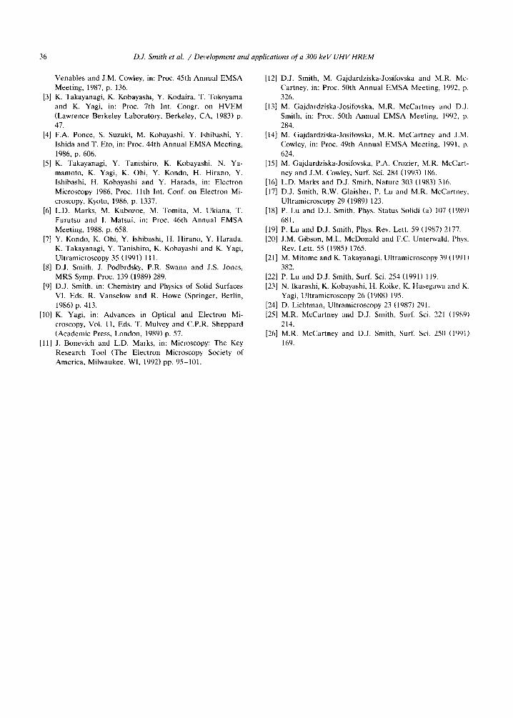
The question of whether the electron beam is making a substantial contribution to the dynami- cal event under observation is not always easily answered, although in some cases it is clear that effects due to the beam are predominant. For example, it is well known that oxides of maximally valent transition-metal oxides are particularly susceptible to electron-stimulated desorption (ESD) of oxygen from surface, and near-surface, regions [24]. Topotactical growth of the corre- sponding lower oxide is often seen under typical conditions used for high-resolution image viewing and recording [25]. To provide bet ter insight into the role of residual vacuum and the specimen temperature in these processes, we have carried out a comprehensive study of electron-beam-in- duced damage and subsequent annealing pro- cesses in futile crystals using the UHV micro- scope [26]. The reduction sequence was not changed by irradiation at room temperature, thus ruling out vacuum as a major factor in the prcvi- ous studies. Studies at higher temperatures led to some interesting results. For example, the futile crystal developed increasingly facetted holes due
Fig. 9. Profile images of Ag surfaces viewed in [110] projection, recorded with time difference of a few minutes at nominal temperature of 115°C.
D.J. Smith et a L / Development and applications of a 300 keV UHV HREM 35
4. Conclusion
The observations described above indicate that the microscope performance has not been com- promised by its UHV conversion. Studies at ele- vated temperature reveal that the specimen holder reaches thermal and mechanical equilib- rium relatively rapidly after changes in heater current. More important, from a scientific point of view, is the fact that the availability of in situ cleaning and annealing treatments in a controlled UHV environment enables us to undertake reli- able surface microscopy studies. R H E E D results have provided a valuable link with traditional surface-science techniques, while reflection elec- tron microscopy and profile imaging have en- abled us to achieve significant insights into novel surface structures and the nature of surface reac- tions. Future activities will include the supply of additional peripheral equipment for the reaction chamber, and an expansion of the range of mate- rials and processes for examination. Overall, it can be concluded that surface electron mi- croscopy represents a valuable complementary method for studying surfaces.
Fig. 10. High-resolution electron micrographs of [001] rutile crystal: (a) after 10 min irradiation at about 80 A/cm 2 show- ing sputter pits, reduced TiO surface phase and intermediary TiO-II phase; (b) same region after annealing for 8 h at 390°C
shows only thin TiO surface layer.
to sputtering but, at temperatures above about 570°C, lower oxides decorating the surface profile were not visible. It was also significant that an- nealing of the beam-damaged rutile crystal at temperatures greater than about 400°C in the absence of the electron beam led to substantial re-oxidation of the reduced phase as shown in fig. 10. Diffusion of oxygen from the bulk of the material is therefore implicated as an important process that should not be overlooked in ESD studies.
Acknowledgements
The UHV conversion of the Philips 430ST has been a joint developmental project between Gatan and the Center for High Resolution Elec- tron Microscopy at Arizona State University that was supported by NSF Grant DMR-830871. We are pleased to acknowledge assistance from Philips personnel, especially R. Mueller and R. de Bruijn, as well as financial support from ONR Grant N00014-86-K-0319. The electron mi- croscopy was conducted at the Center for High Resolution Electron Microscopy at Arizona State University supported by NSF Grants DMR-86- 11609 and DMR-89-13384.
References
[1] M.L. McDonald, J.M. Gibson and F.C. Unterwald, Rev. Sci. Instr. 60 (1989) 700.
[2] P.R. Swann, J.S. Jones, O.L. Krivanek, D.J. Smith, J.A.
36 D.J. Smith et al. / Development and applications of a 300 keV UHV HREM
Venables and J.M. Cowley, in: Proc. 45th Annual EMSA Meeting, 1987, p. 136.
[3] K. Takayanagi, K. Kobayashi, Y. Kodaira, T. Tokoyama and K. Yagi, in: Proc. 7th Int. Congr. on HVEM (Lawrence Berkeley Laboratory, Berkeley, CA, 1983) p. 47.
[4] F.A. Ponce, S. Suzuki, M. Kobayashi, Y. Ishibashi, Y. lshida and T. Eto, in: Proc. 44th Annual EMSA Meeting, 1986, p. 606.
[5] K. Takayanagi, Y. Tanishiro, K. Kobayashi, N. Ya- mamoto, K. Yagi, K. Ohi, Y. Kondo, H. Hirano, Y. Ishibashi, H. Kobayashi and Y. Harada, in: Electron Microscopy 1986, Proc. l lth Int. Conf. on Electron Mi- croscopy, Kyoto, 1986, p. 1337.
[6] L.D. Marks, M. Kubozoe, M. Tomita, M. Ukiana, T. Furutsu and I. Matsui, in: Proc. 46th Annual EMSA Meeting, 1988, p. 658.
[7] Y. Kondo, K. Ohi, Y. Ishibashi, H. Hirano, Y. Harada, K. Takayanagi, Y. Tanishiro, K. Kobayashi and K. Yagi, Ultramicroscopy 35 (1991) 111.
[8] D.J. Smith, J. Podbrdsky, P.R. Swann and J.S. Jones, MRS Symp. Proc. 139 (1989) 289.
[9] D.J. Smith, in: Chemistry and Physics of Solid Surfaces VI, Eds. R. Vanselow and R. Howe (Springer, Berlin, 1986) p. 413.
[10] K. Yagi, in: Advances in Optical and Electron Mi- croscopy, Vol. 11, Eds. T. Mulvey and C.P.R. Sheppard (Academic Press, London, 1989) p. 57.
[11] J. Bonevich and L.D. Marks, in: Microscopy: The Key Research Tool (The Electron Microscopy Society of America, Milwaukee, WI, 1992) pp. 95-101.
[12] D.J. Smith, M. Gajdardziska-Josifovska and M.R. Mc- Cartney, in: Proc. 50th Annual EMSA Meeting, 1992, p. 326.
[13] M. Gajdardziska-Josifovska, M.R. McCartney and D.J. Smith, in: Proc. 50th Annual EMSA Meeting, 1992, p. 284.
[14] M. Gajdardziska-Josifovska, M.R. McCartney and J.M. Cowley, in: Proc. 49th Annual EMSA Meeting, 1991, p. 624.
[15] M. Gajdardziska-Josifovska, P.A. Crozier, M.R. McCart- ney and J.M. Cowley, Surf. Sci. 284 (1993) 186.
[16] L.D. Marks and D.J. Smith, Nature 303 (1983) 316. [17] D.J. Smith, R.W. Glaisher, P. Lu and M.R. McCartney,
Ultramicroscopy 29 (1989) 123. [18] P. Lu and D.J. Smith, Phys. Status Solidi (a) 107 (1989)
681. [19] P. Lu and D.J. Smith, Phys. Rev. Lett. 59 (1987) 2177. [20] J.M. Gibson, M.L. McDonald and F.C. Unterwald, Phys.
Rev. Lett. 55 (1985) 1765. [21] M. Mitome and K. Takayanagi, Ultramicroscopy 39 (1991)
382. [22] P. Lu and D.J. Smith, Surf. Sci. 254 (1991) 119. [23] N. Ikarashi, K. Kobayashi, H. Koike, K. Hasegawa and K.
Yagi, Ultramicroscopy 26 (1988) 195. [24] D. Lichtman, Ultramicroscopy 23 (1987) 291. [25] M.R. McCartney and D.J. Smith, Surf. Sci. 221 (1989)
214. [26] M.R. McCartney and D.J. Smith, Surf. Sci. 250 (1991)
169.