Embed Size (px)
Citation preview

Revision 1.0
Development Board EPC9148Quick Start Guide 48 V Three-level Synchronous Buck Converter, Using EPC2053
QUICK START GUIDE EPC9148
EPC – POWER CONVERSION TECHNOLOGY LEADER | EPC-CO.COM | ©2021 | | 2
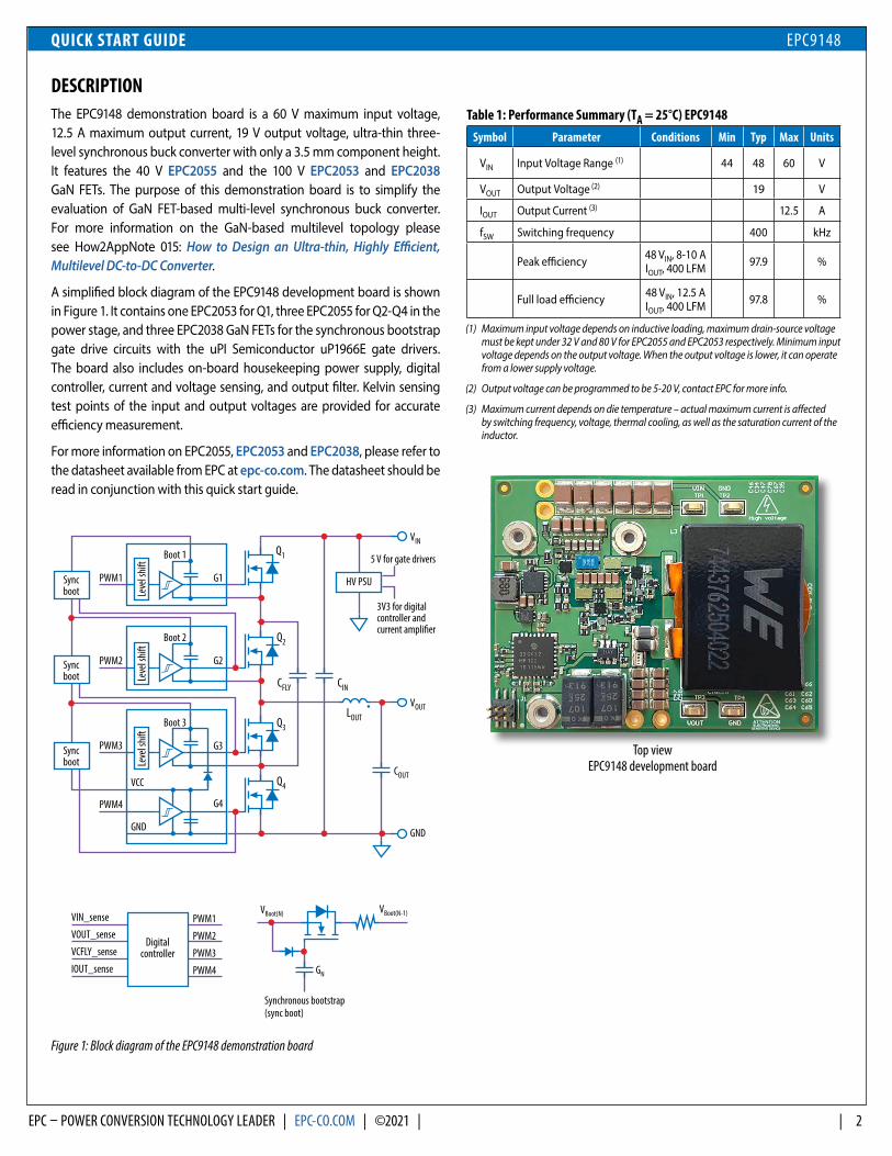
DESCRIPTION The EPC9148 demonstration board is a 60 V maximum input voltage, 12.5 A maximum output current, 19 V output voltage, ultra-thin three-level synchronous buck converter with only a 3.5 mm component height. It features the 40 V EPC2055 and the 100 V EPC2053 and EPC2038 GaN FETs. The purpose of this demonstration board is to simplify the evaluation of GaN FET-based multi-level synchronous buck converter. For more information on the GaN-based multilevel topology please see How2AppNote 015: How to Design an Ultra-thin, Highly Efficient, Multilevel DC-to-DC Converter.
A simplified block diagram of the EPC9148 development board is shown in Figure 1. It contains one EPC2053 for Q1, three EPC2055 for Q2-Q4 in the power stage, and three EPC2038 GaN FETs for the synchronous bootstrap gate drive circuits with the uPI Semiconductor uP1966E gate drivers. The board also includes on-board housekeeping power supply, digital controller, current and voltage sensing, and output filter. Kelvin sensing test points of the input and output voltages are provided for accurate efficiency measurement.
For more information on EPC2055, EPC2053 and EPC2038, please refer to the datasheet available from EPC at epc-co.com. The datasheet should be read in conjunction with this quick start guide.
Table 1: Performance Summary (TA = 25°C) EPC9148 Symbol Parameter Conditions Min Typ Max Units
VIN Input Voltage Range (1) 44 48 60 V
VOUT Output Voltage (2) 19 V
IOUT Output Current (3) 12.5 A
fSW Switching frequency 400 kHz
Peak efficiency 48 VIN, 8-10 A IOUT, 400 LFM 97.9 %
Full load efficiency 48 VIN, 12.5 A IOUT, 400 LFM 97.8 %
(1) Maximum input voltage depends on inductive loading, maximum drain-source voltage must be kept under 32 V and 80 V for EPC2055 and EPC2053 respectively. Minimum input voltage depends on the output voltage. When the output voltage is lower, it can operate from a lower supply voltage.
(2) Output voltage can be programmed to be 5-20 V, contact EPC for more info.
(3) Maximum current depends on die temperature – actual maximum current is affected by switching frequency, voltage, thermal cooling, as well as the saturation current of the inductor.
Top view EPC9148 development board
Figure 1: Block diagram of the EPC9148 demonstration board
Boot 1
PWM1 G1
Q1
Q2
CFLY CIN
LOUTQ3
Q4
Leve
l shif
t
Boot 2
PWM2 G2
Leve
l shif
t
Syncboot
Boot 3
PWM4
Synchronous bootstrap(sync boot)
VCC
GND
GN
VBoot(N) VBoot(N-1)
G3
G4
PWM3
Leve
l shif
t
Syncboot
Syncboot
HV PSU
3V3 for digitalcontroller andcurrent ampli�er
5 V for gate drivers
VIN
VOUT
GND
COUT
PWM1
PWM2
PWM3
PWM4
VIN_sense
VOUT_sense
VCFLY_sense
IOUT_sense
Digitalcontroller
QUICK START GUIDE EPC9148
EPC – POWER CONVERSION TECHNOLOGY LEADER | EPC-CO.COM | ©2021 | | 3
VIN Supply(Note Polarity)
VIN Supply(Note Polarity)
Input voltagemeasurement(HIGH VOLTAGE!)
GND probing
Switch-node probing
Output voltagemeasurement
DC Load
DC Load
V
+
+
_
_
V
60 VINmax
60 VINmax
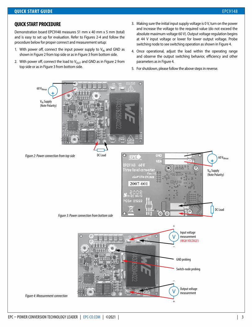
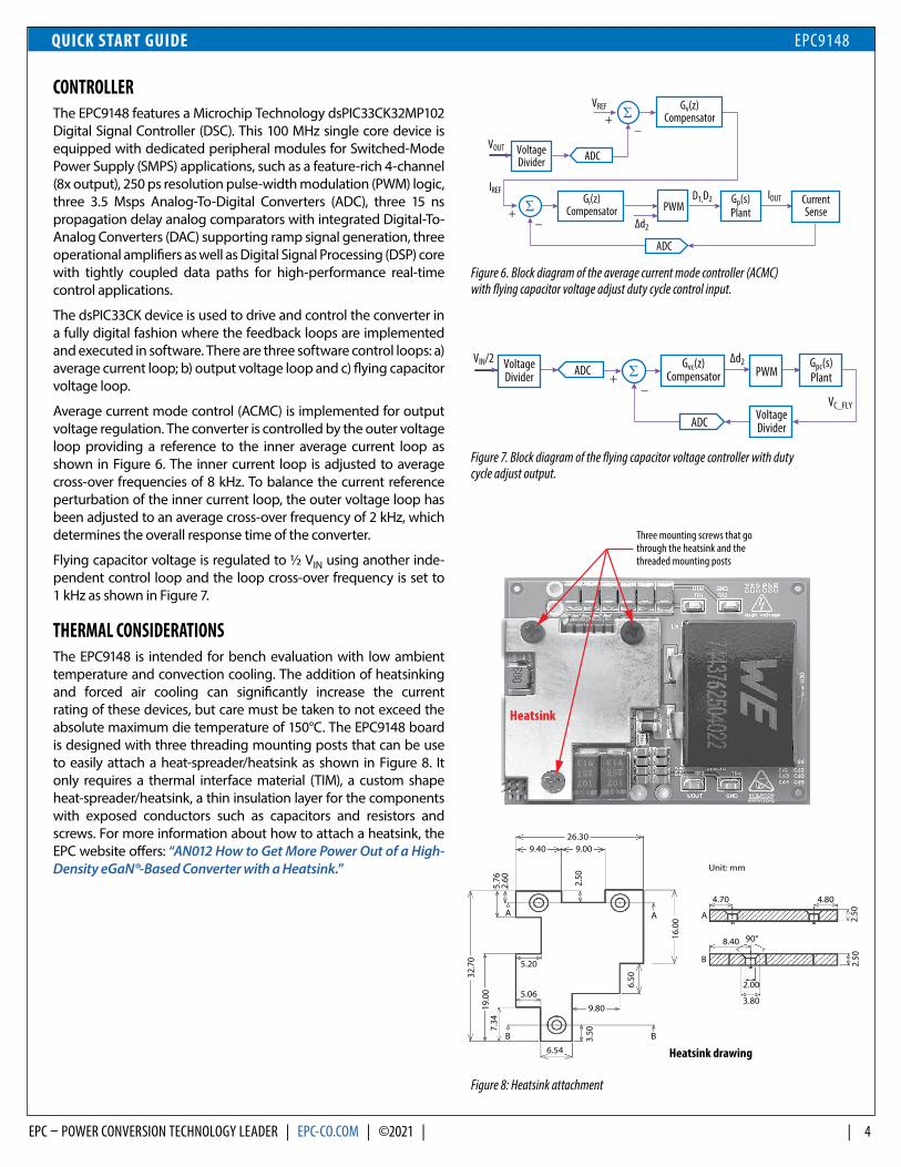
QUICK START PROCEDURE Demonstration board EPC9148 measures 51 mm x 40 mm x 5 mm (total) and is easy to set up for evaluation. Refer to Figures 2-4 and follow the procedure below for proper connect and measurement setup:
1. With power off, connect the input power supply to VIN and GND as shown in Figure 2 from top side or as in Figure 3 from bottom side.
2. With power off, connect the load to VOUT and GND as in Figure 2 from top side or as in Figure 3 from bottom side.
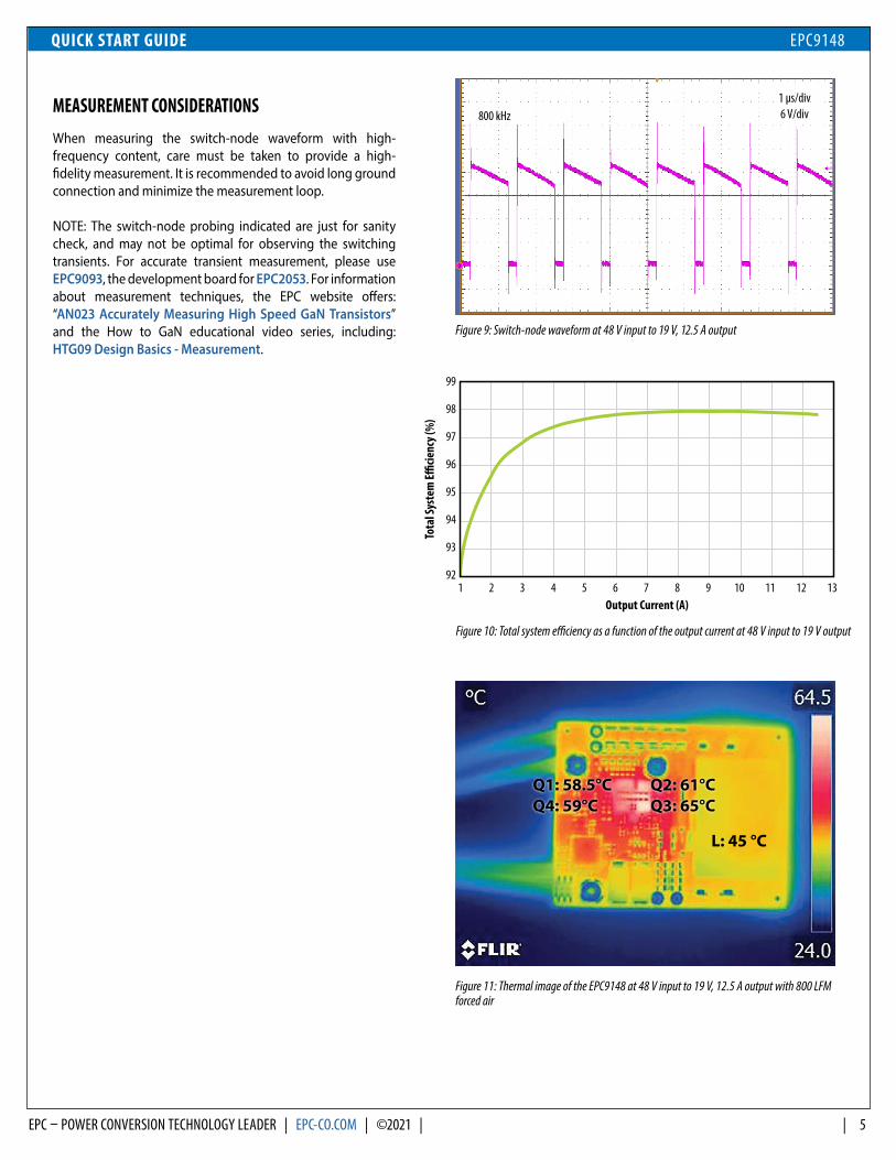
3. Making sure the initial input supply voltage is 0 V, turn on the power and increase the voltage to the required value (do not exceed the absolute maximum voltage 60 V). Output voltage regulation begins at 44 V input voltage or lower for lower output voltage. Probe switching node to see switching operation as shown in Figure 4.
4. Once operational, adjust the load within the operating range and observe the output switching behavior, efficiency and other parameters as in Figure 4.
5. For shutdown, please follow the above steps in reverse.
Figure 2: Power connection from top side
Figure 4: Measurement connection
Figure 3: Power connection from bottom side
QUICK START GUIDE EPC9148
EPC – POWER CONVERSION TECHNOLOGY LEADER | EPC-CO.COM | ©2021 | | 4
CONTROLLERThe EPC9148 features a Microchip Technology dsPIC33CK32MP102 Digital Signal Controller (DSC). This 100 MHz single core device is equipped with dedicated peripheral modules for Switched-Mode Power Supply (SMPS) applications, such as a feature-rich 4-channel (8x output), 250 ps resolution pulse-width modulation (PWM) logic, three 3.5 Msps Analog-To-Digital Converters (ADC), three 15 ns propagation delay analog comparators with integrated Digital-To-Analog Converters (DAC) supporting ramp signal generation, three operational amplifiers as well as Digital Signal Processing (DSP) core with tightly coupled data paths for high-performance real-time control applications.
The dsPIC33CK device is used to drive and control the converter in a fully digital fashion where the feedback loops are implemented and executed in software. There are three software control loops: a) average current loop; b) output voltage loop and c) flying capacitor voltage loop.
Average current mode control (ACMC) is implemented for output voltage regulation. The converter is controlled by the outer voltage loop providing a reference to the inner average current loop as shown in Figure 6. The inner current loop is adjusted to average cross-over frequencies of 8 kHz. To balance the current reference perturbation of the inner current loop, the outer voltage loop has been adjusted to an average cross-over frequency of 2 kHz, which determines the overall response time of the converter.
Flying capacitor voltage is regulated to ½ VIN using another inde-pendent control loop and the loop cross-over frequency is set to 1 kHz as shown in Figure 7.
THERMAL CONSIDERATIONSThe EPC9148 is intended for bench evaluation with low ambient temperature and convection cooling. The addition of heatsinking and forced air cooling can significantly increase the current rating of these devices, but care must be taken to not exceed the absolute maximum die temperature of 150°C. The EPC9148 board is designed with three threading mounting posts that can be use to easily attach a heat-spreader/heatsink as shown in Figure 8. It only requires a thermal interface material (TIM), a custom shape heat-spreader/heatsink, a thin insulation layer for the components with exposed conductors such as capacitors and resistors and screws. For more information about how to attach a heatsink, the EPC website offers: “AN012 How to Get More Power Out of a High-Density eGaN®-Based Converter with a Heatsink.”
Figure 8: Heatsink attachment
Figure 7. Block diagram of the flying capacitor voltage controller with duty cycle adjust output.
ADC
Δd2
D1,D2IREF
VREF
+
+
_
_
VOUTADC
PWM CurrentSense
IOUTGi(z)CompensatorΣ
Gv(z)CompensatorΣ
Gp(s)Plant
VoltageDivider
ADC
Δd2
VC_FLY
+ _
VIN/2ADC PWM
Gvc(z)CompensatorΣ Gpc(s)
PlantVoltageDivider
VoltageDivider
Figure 6. Block diagram of the average current mode controller (ACMC) with flying capacitor voltage adjust duty cycle control input.
Heatsink
Heatsink drawing
Three mounting screws that gothrough the heatsink and thethreaded mounting posts
26.30
A
5.20
6.54
9.80
5.06
B B
A A
B
4.70
Unit: mm
8.40
2.00
3.80
4.80
2.50
2.50
90°
2.50
32.7
0
19.0
0
6.50
16.0
0
3.507.
342.
605.
76
9.40 9.00
QUICK START GUIDE EPC9148
EPC – POWER CONVERSION TECHNOLOGY LEADER | EPC-CO.COM | ©2021 | | 5
Figure 9: Switch-node waveform at 48 V input to 19 V, 12.5 A output
Figure 10: Total system efficiency as a function of the output current at 48 V input to 19 V output
Figure 11: Thermal image of the EPC9148 at 48 V input to 19 V, 12.5 A output with 800 LFM forced air
MEASUREMENT CONSIDERATIONS When measuring the switch-node waveform with high-frequency content, care must be taken to provide a high-fidelity measurement. It is recommended to avoid long ground connection and minimize the measurement loop.
NOTE: The switch-node probing indicated are just for sanity check, and may not be optimal for observing the switching transients. For accurate transient measurement, please use EPC9093, the development board for EPC2053. For information about measurement techniques, the EPC website offers: “AN023 Accurately Measuring High Speed GaN Transistors” and the How to GaN educational video series, including: HTG09 Design Basics - Measurement.
800 kHz1 µs/div6 V/div
99
98
97
96
95
94
93
921 2 3
Output Current (A)
Tota
l Sys
tem
E�cie
ncy (
%)
4 5 6 7 8 9 10 11 12 13
Q1: 58.5°CQ4: 59°C
Q2: 61°CQ3: 65°C
L: 45 °C
QUICK START GUIDE EPC9148
EPC – POWER CONVERSION TECHNOLOGY LEADER | EPC-CO.COM | ©2021 | | 6
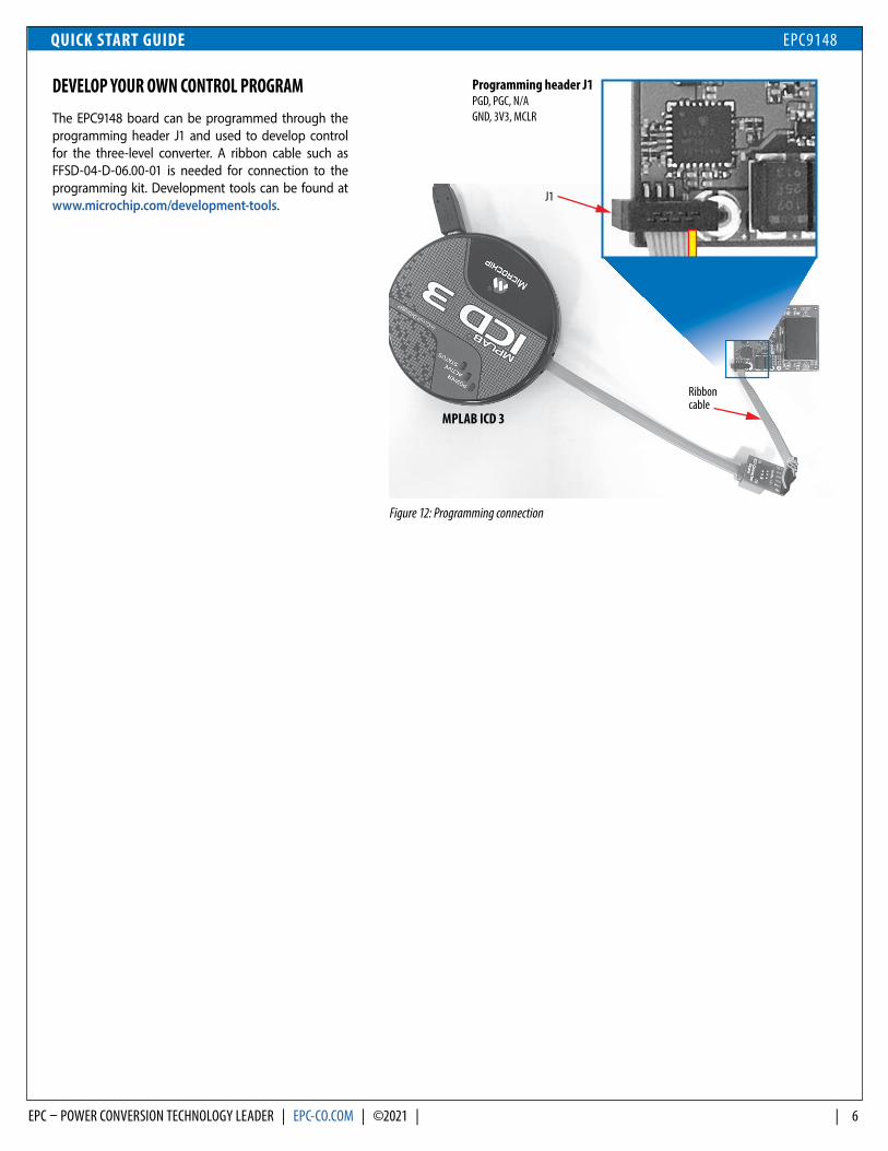
DEVELOP YOUR OWN CONTROL PROGRAMThe EPC9148 board can be programmed through the programming header J1 and used to develop control for the three-level converter. A ribbon cable such as FFSD-04-D-06.00-01 is needed for connection to the programming kit. Development tools can be found at www.microchip.com/development-tools.
MPLAB ICD 3
Programming header J1PGD, PGC, N/AGND, 3V3, MCLR
J1
Ribboncable
Figure 12: Programming connection
QUICK START GUIDE EPC9148
EPC – POWER CONVERSION TECHNOLOGY LEADER | EPC-CO.COM | ©2021 | | 7
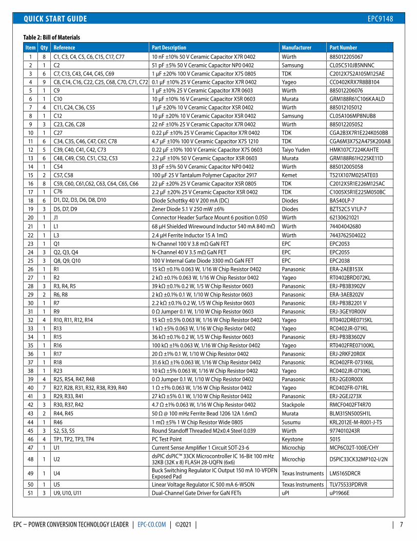
Table 2: Bill of MaterialsItem Qty Reference Part Description Manufacturer Part Number
1 8 C1, C3, C4, C5, C6, C15, C17, C77 10 nF ±10% 50 V Ceramic Capacitor X7R 0402 Würth 8850122050672 1 C2 51 pF ±5% 50 V Ceramic Capacitor NP0 0402 Samsung CL05C510JB5NNNC3 6 C7, C13, C43, C44, C45, C69 1 µF ±20% 100 V Ceramic Capacitor X7S 0805 TDK C2012X7S2A105M125AE4 9 C8, C14, C16, C22, C25, C68, C70, C71, C72 0.1 µF ±10% 25 V Ceramic Capacitor X7R 0402 Yageo CC0402KRX7R8BB1045 1 C9 1 µF ±10% 25 V Ceramic Capacitor X7R 0603 Würth 8850122060766 1 C10 10 µF ±10% 16 V Ceramic Capacitor X5R 0603 Murata GRM188R61C106KAALD7 4 C11, C24, C36, C55 1 µF ±20% 10 V Ceramic Capacitor X5R 0402 Würth 8850121050128 1 C12 10 µF ±20% 10 V Ceramic Capacitor X5R 0402 Samsung CL05A106MP8NUB89 3 C23, C26, C28 22 nF ±10% 25 V Ceramic Capacitor X7R 0402 Würth 885012205052
10 1 C27 0.22 µF ±10% 25 V Ceramic Capacitor X7R 0402 TDK CGA2B3X7R1E224K050BB11 6 C34, C35, C46, C47, C67, C78 4.7 µF ±10% 100 V Ceramic Capacitor X7S 1210 TDK CGA6M3X7S2A475K200AB12 5 C39, C40, C41, C42, C73 0.22 µF ±10% 100 V Ceramic Capacitor X7S 0603 Taiyo Yuden HMK107C7224KAHTE13 6 C48, C49, C50, C51, C52, C53 2.2 µF ±10% 50 V Ceramic Capacitor X5R 0603 Murata GRM188R61H225KE11D14 1 C54 33 pF ±5% 50 V Ceramic Capacitor NP0 0402 Würth 88501200505815 2 C57, C58 100 µF 25 V Tantalum Polymer Capacitor 2917 Kemet T521X107M025ATE0316 8 C59, C60, C61,C62, C63, C64, C65, C66 22 µF ±20% 25 V Ceramic Capacitor X5R 0805 TDK C2012X5R1E226M125AC17 1 C76 2.2 µF ±20% 25 V Ceramic Capacitor X5R 0402 TDK C1005X5R1E225M050BC18 6 D1, D2, D3, D6, D8, D10 Diode Schottky 40 V 200 mA (DC) Diodes BAS40LP-7 19 3 D5, D7, D9 Zener Diode 5.1 V 250 mW ±6% Diodes BZT52C5 V1LP-720 1 J1 Connector Header Surface Mount 6 position 0.050 Würth 6213062102121 1 L1 68 µH Shielded Wirewound Inductor 540 mA 840 mΩ Würth 7440404268022 1 L3 2.4 µH Ferrite Inductor 15 A 1mΩ Würth 744376250402223 1 Q1 N-Channel 100 V 3.8 mΩ GaN FET EPC EPC205324 3 Q2, Q3, Q4 N-Channel 40 V 3.5 mΩ GaN FET EPC EPC205525 3 Q8, Q9, Q10 100 V Internal Gate Diode 3300 mΩ GaN FET EPC EPC203826 1 R1 15 kΩ ±0.1% 0.063 W, 1/16 W Chip Resistor 0402 Panasonic ERA-2AEB153X 27 1 R2 2 kΩ ±0.1% 0.063 W, 1/16 W Chip Resistor 0402 Yageo RT0402BRD072KL28 3 R3, R4, R5 39 kΩ ±0.1% 0.2 W, 1/5 W Chip Resistor 0603 Panasonic ERJ-PB3B3902V29 2 R6, R8 2 kΩ ±0.1% 0.1 W, 1/10 W Chip Resistor 0603 Panasonic ERA-3AEB202V 30 1 R7 2.2 kΩ ±0.1% 0.2 W, 1/5 W Chip Resistor 0603 Panasonic ERJ-PB3B2201 V31 1 R9 0 Ω Jumper 0.1 W, 1/10 W Chip Resistor 0603 Panasonic ERJ-3GEY0R00V32 4 R10, R11, R12, R14 15 kΩ ±0.5% 0.063 W, 1/16 W Chip Resistor 0402 Yageo RT0402DRE0715KL33 1 R13 1 kΩ ±5% 0.063 W, 1/16 W Chip Resistor 0402 Yageo RC0402JR-071KL34 1 R15 36 kΩ ±0.1% 0.2 W, 1/5 W Chip Resistor 0603 Panasonic ERJ-PB3B3602V35 1 R16 100 kΩ ±1% 0.063 W, 1/16 W Chip Resistor 0402 Yageo RT0402FRE07100KL36 1 R17 20 Ω ±1% 0.1 W, 1/10 W Chip Resistor 0402 Panasonic ERJ-2RKF20R0X37 1 R18 31.6 kΩ ±1% 0.063 W, 1/16 W Chip Resistor 0402 Panasonic RC0402FR-0731K6L38 1 R23 10 kΩ ±5% 0.063 W, 1/16 W Chip Resistor 0402 Yageo RC0402JR-0710KL39 4 R25, R54, R47, R48 0 Ω Jumper 0.1 W, 1/10 W Chip Resistor 0402 Panasonic ERJ-2GE0R00X40 7 R27, R28, R31, R32, R38, R39, R40 1 Ω ±1% 0.063 W, 1/16 W Chip Resistor 0402 Yageo RC0402FR-071RL41 3 R29, R33, R41 27 kΩ ±5% 0.1 W, 1/10 W Chip Resistor 0402 Panasonic ERJ-2GEJ273X42 3 R30, R37, R42 4.7 Ω ±1% 0.063 W, 1/16 W Chip Resistor 0402 Stackpole RMCF0402FT4R7043 2 R44, R45 50 Ω @ 100 mHz Ferrite Bead 1206 12A 1.6mΩ Murata BLM31SN500SH1L44 1 R46 1 mΩ ±5% 1 W Chip Resistor Wide 0805 Susumu KRL2012E-M-R001-J-T545 3 S2, S3, S5 Round Standoff Threaded M2x0.4 Steel 0.039 Würth 9774010243R46 4 TP1, TP2, TP3, TP4 PC Test Point Keystone 501547 1 U1 Current Sense Amplifier 1 Circuit SOT-23-6 Microchip MCP6C02T-100E/CHY
48 1 U2 dsPIC dsPIC™ 33CK Microcontroller IC 16-Bit 100 mHz 32KB (32K x 8) FLASH 28-UQFN (6x6) Microchip DSPIC33CK32MP102-I/2N
49 1 U4 Buck Switching Regulator IC Output 150 mA 10-VFDFN Exposed Pad Texas Instruments LM5165DRCR
50 1 U5 Linear Voltage Regulator IC 500 mA 6-WSON Texas Instruments TLV75533PDRVR51 3 U9, U10, U11 Dual-Channel Gate Driver for GaN FETs uPI uP1966E
QUICK START GUIDE EPC9148
EPC – POWER CONVERSION TECHNOLOGY LEADER | EPC-CO.COM | ©2021 | | 8
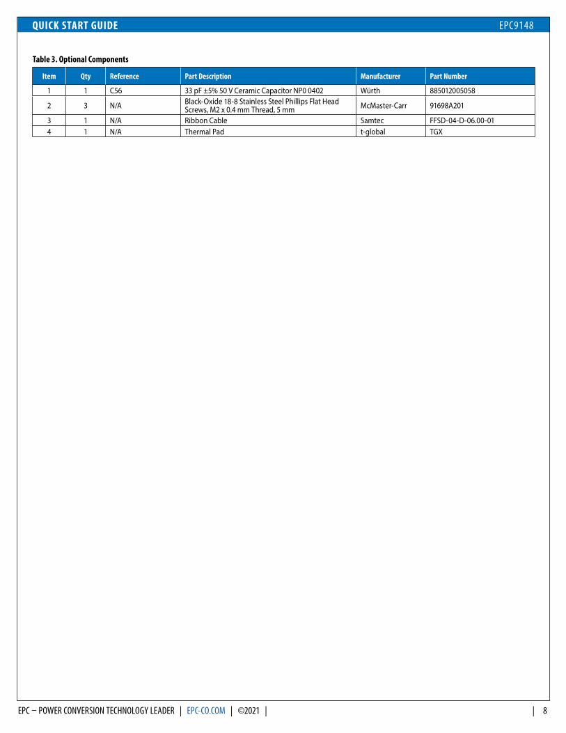
Table 3. Optional Components
Item Qty Reference Part Description Manufacturer Part Number
1 1 C56 33 pF ±5% 50 V Ceramic Capacitor NP0 0402 Würth 885012005058
2 3 N/A Black-Oxide 18-8 Stainless Steel Phillips Flat Head Screws, M2 x 0.4 mm Thread, 5 mm McMaster-Carr 91698A201
3 1 N/A Ribbon Cable Samtec FFSD-04-D-06.00-01 4 1 N/A Thermal Pad t-global TGX
QUICK START GUIDE EPC9148
EPC – POWER CONVERSION TECHNOLOGY LEADER | EPC-CO.COM | ©2021 | | 9
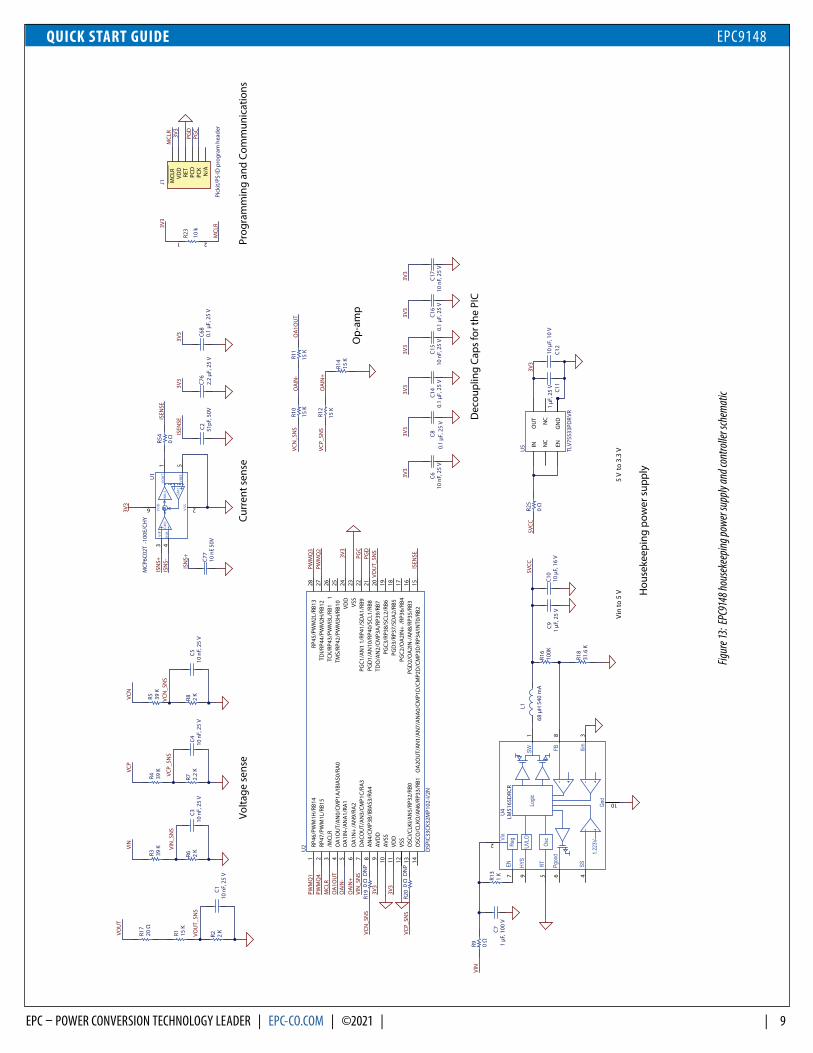
Figur
e 13:
EPC9
148 h
ouse
keep
ing po
wer s
upply
and c
ontro
ller s
chem
atic
15 K
R1 2 K
R2
10 n
F , 2
5 V
C1
39 K
R3 2 K
R6
10 n
F , 2
5 V
C3 Volta
ge s
ense
10 n
F , 2
5 V
C4
VCN
10 n
F , 2
5 V
C5
VCN
_SN
S
Pick
it/PS
-ID p
rogr
am h
eade
r
Prog
ram
min
g an
d Co
mm
unic
atio
ns
10 k
1 2
R23
Curr
ent s
ense1
26
4
5
3G
M1
GM
2
RM3
VO
UT
VRE
F
VIMVIP
VSS
VD
DU
1M
CP6C
02T
-100
E/CH
Y
51pF
, 50V
C2
39 K
R4 2.2
KR7
2 K
R839 K
R5
68 μ
H 5
40 m
A
L1
10 μ
F , 1
6 V
C10
1 μF
, 10
0 V
C7
10
Reg
Osc
3
HYS
Logic
SS
2
5
Gnd
Vin
Ilim
1 8
UVLO
RTEN
SW
47 9
FB6
Pgoo
d 1.223
V
U4
LM51
65D
RCR
1 μF
, 25
VC9
31.6
KR1
8
100K
R16
10 μ
F , 1
0 V
C12
1 μF
, 25
V C11
Hou
seke
epin
g po
wer
sup
ply
Vin
to 5
V5
V to
3.3
V
3V3
IN ENG
ND
OU
T
NC
NC
U5
TLV7
5533
PDR
VR
0.1
μF ,
25 V
C68
2.2
μF ,
25 V
C76
10 n
F, 50
VC7
7
ISN
S+
ISEN
SE
MCL
RVD
DRE
TPC
DPC
KN
/A
J1M
CLR
3V3
PGD
0 Ω
R9
1 K
R13
VOU
T
VOU
T_SN
S
VIN
_SN
S
VIN
VCP
VCP_
SNS
ISEN
SE3V
33V
3
3V3
MCL
R
3V3
VIN
PGC
0 Ω
R25
5VCC
5VCC
ISN
S+IS
NS-
0 Ω
R54
0.1
μF ,
25 V
C80.
1 μF
, 25
VC1
410
nF ,
25
VC6
0.1
μF ,
25 V
C16
RP46
/PW
M1H
/RB1
41
RP47
/PW
M1L
/RB1
52
/MCL
R3
OA
1OU
T/A
N0/
CMP1
A/IB
IAS0
/RA
04
OA
1IN
-/A
NA
1/RA
15
OA
1N+
/AN
9/RA
26
DA
COU
T/A
N3/
CMP1
C/RA
37
AN
4/CM
P3B/
IBIA
S3/R
A4
8
AVD
D9
AVSS
10
VDD
11
VSS
12
OSC
I/CLK
I/AN
5/RP
32/R
B013
OSC
O/C
LKO
/AN
6/RP
33/R
B114
OA
2OU
T/A
N1/
AN
7/A
NA
0/CM
P1D
/CM
P2D
/CM
P3D
/RP3
4/IN
T0/R
B215
PGD
2/O
A2I
N-/
AN
8/RP
35/R
B316
PGC2
/OA
2IN
+/R
P36/
RB4
17PG
D3/
RP37
/SD
A2/
RB5
18PG
C3/R
P38/
SCL2
/RB6
19TD
O/A
N2/
CMP3
A/R
P39/
RB7
20PG
D1/
AN
10/R
P40/
SCL1
/RB8
21PG
C1/A
N1
1/RP
41/S
DA
1/RB
922
VSS
23VD
D24
TMS/
RP42
/PW
M3H
/RB1
025
TCK/
RP43
/PW
M3L
/RB1
126
TDI/R
P44/
PWM
2H/R
B12
27RP
45/P
WM
2L/R
B13
28U
2
DSP
IC33
CK32
MP1
02-I/
2N
MCL
R
3V3
3V3
3V3
PWM
Q1
PWM
Q4
OA
IN-
OA
IN+
VIN
_SN
S
ISEN
SEPGD
PGC
VOU
T_SN
S
PWM
Q2
PWM
Q3
0 Ω
R19
DN
P
0 Ω
R20
DN
P
VCN
_SN
S
VCP_
SNS
3V3
3V3
3V3
3V3
10 n
F , 2
5 V
C15
3V3
10 n
F , 2
5 V
C17
3V3
15 K
R12
15 K
R14
15 K
R10
15 K
R11
VCP_
SNS
VCN
_SN
SO
AIN
-
OA
IN+
OA
1OU
T
OA
1OU
T
Op-
amp
Dec
oupl
ing
Caps
for t
he P
IC
20 Ω
R17
QUICK START GUIDE EPC9148
EPC – POWER CONVERSION TECHNOLOGY LEADER | EPC-CO.COM | ©2021 | | 10
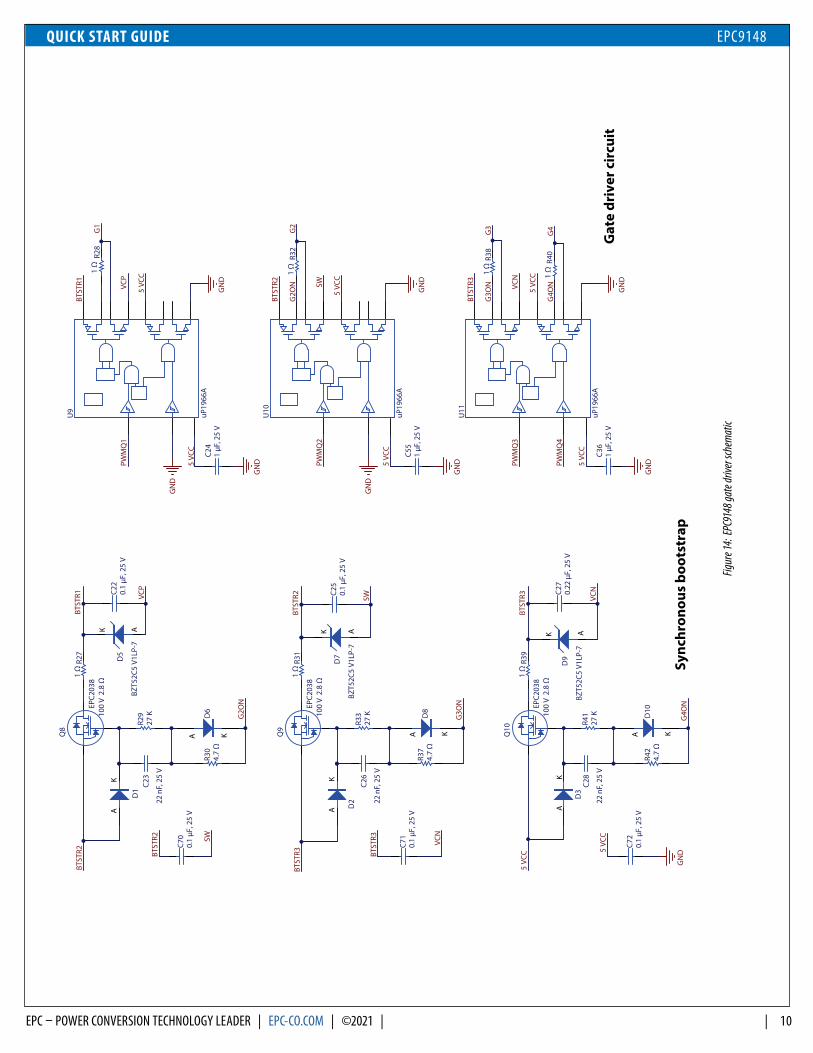
Figur
e 14:
EPC9
148 g
ate d
river
schem
atic
U9
uP19
66A
U10
uP19
66A
U11
uP19
66A
GN
D1 Ω
R40
G4
1 Ω
R38
G3
1 μF
, 25
VC3
6
BTST
R3
GN
D
GN
D
1 Ω
R32
G2
BTST
R2
GN
D
1 Ω
R28
1 μF
, 25
VC2
4
GN
D
22 n
F , 2
5 V
C23
100
V 2
.8 Ω
Q8
EPC2
038
5 VC
C
D5
BZT5
2C5
V1LP
-7
27 K
R29
4.7
ΩR3
0
G3O
N
Sync
hron
ous
boot
stra
p
Gat
e dr
iver
cir
cuit
G4O
N
1 Ω
R27
0.1
μF ,
25 V
C22
22 n
F , 2
5 V
C26
100
V 2
.8 Ω
Q9
EPC2
038
D7
BZT5
2C5
V1LP
-7
27 K
R33
4.7
ΩR3
7
G3O
N
1 Ω
R31
0.1
μF ,
25 V
C25
BTST
R2 SW
SW
5 VC
C
22 n
F , 2
5 V
C28
100
V 2
.8 Ω
Q10
EPC2
038
D9
BZT5
2C5
V1LP
-7
27 K
R41
4.7
ΩR4
2
1 Ω
R39
0.22
μF ,
25
VC2
7
BTST
R3VC
N
5 VC
C
1 μF
, 25
VC5
5
GN
D
D6
D8
D10
0.1
μF ,
25 V
C72
GN
D5 VC
C
0.1
μF ,
25 V
C71
0.1
μF ,
25 V
C70
GN
D
D1
BTST
R2
D2 D
3
5 VC
C
VCP
BTST
R1
SW
BTST
R2
G2O
N
BTST
R3 VCN
BTST
R3
G4O
N
VCN
PWM
Q1
BTST
R1
G1
VCP
5 VC
C
G2O
N
PWM
Q2
5 VC
C
PWM
Q3
PWM
Q4
5 VC
C
AK
AK
A K
AK
AK AK AK
A K A K
GN
D
QUICK START GUIDE EPC9148
EPC – POWER CONVERSION TECHNOLOGY LEADER | EPC-CO.COM | ©2021 | | 11
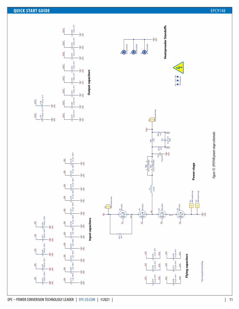
Figur
e 15:
EPC9
148 p
ower
stage
sche
mat
ic
GN
D
VIN
2.2
μF ,
50 V
C50
2.2
μF ,
50 V
C48
2.2
μF ,
50 V
C53
2.2
μF ,
50 V
C51
2.2
μF ,
50 V
C49
2.2
μF ,
50 V
C52
G4
G3
G2
G1
Pow
er s
tage
EPC2
055
Q2 EP
C205
5
Q3
EPC2
055
Q4
VOU
T
0 Ω
R47
33 p
F , 5
0 V
C56
DN
P
0 Ω
R48
12
50 Ω
@ 1
00 M
Hz
R45
33 p
F , 50
V
C54 G
ND
12
50 Ω
@ 1
00 M
Hz
R44
22 μ
F , 2
5 V
C62
1 μF
, 10
0 V
C43
1 μF
, 10
0 V
C44
1 μF
, 10
0 V
C45
220
nF ,
100
VC3
9
GN
D
220
nF ,
100
VC4
0
GN
D
220
nF ,
100
VC4
1
GN
D
220
nF ,
100
VC4
2
GN
D
GN
D
4.7
μF ,
100
VC4
64.
7 μF
, 10
0 V
C47
22 μ
F , 2
5 V
C63
22 μ
F , 2
5 V
C61
22 μ
F , 2
5 V
C59
22 μ
F , 2
5 V
C60
22 μ
F , 2
5 V
C66
22 μ
F , 2
5 V
C65
22 μ
F , 2
5 V
C64
FD1
PCB
Fidu
cial
FD2
FD3
1 μF
, 10
0 V
C69
220
nF ,
100
VC7
3
GN
D
36 K
R15*
* St
art-
up p
aten
t pen
ding
4.7
μF ,
100
VC3
44.
7 μF
, 10
0 V
C35
4.7
μF ,
100
VC6
74.
7 μF
, 10
0 V
C78
SMD
pro
be lo
op1
TP2
SMD
pro
be lo
op
1
TP1
2.4
μHL3
VIN
VIN
SW
ISNS+
ISNS-
Q1
EPC2
053
S2 9774
0102
43R
S5 9774
0102
43R
GN
D
Hea
tspr
eade
r Sta
ndo�
s
S3 9774
0102
43R
1 μF
, 10
0 V
C13
1 m
Ω
R46
VCN
VCN
VCN
VCP
VCP
VCP
VCN
VCN
VCN
VCP
VCP
VCP
GN
DG
ND
GN
DG
ND
GN
DG
ND
GN
DG
ND
GN
DG
ND
VIN
VIN
VIN
VIN
VIN
VIN
VIN
VIN
VIN
VIN
VIN
VIN
VIN
VIN
Flyi
ng c
apac
itor
s
Inpu
t cap
acit
ors
SMD
pro
be lo
op
1
TP3
SMD
pro
be lo
op1
TP4
+10
0 μF
, 25
VC5
7+
100
μF, 2
5 V
C58
GN
D
VOU
T
GN
D
VOU
T
GN
D
VOU
T
GN
D
VOU
T
GN
D
VOU
T
GN
D
VOU
T
GN
D
VOU
T
GN
D
VOU
T
GN
D
VOU
T
GN
D
VOU
T
Out
put c
apac
itor
sVCN
VCP
QUICK START GUIDE EPC9148
EPC – POWER CONVERSION TECHNOLOGY LEADER | EPC-CO.COM | ©2021 | | 12
EPC would like to acknowledge Microchip Technology Inc. (www.microchip.com) for their support of this project.
Microchip Technology Incorporated is a leading provider of smart, connected and secure embedded control solutions. Its easy-to-use development tools and comprehensive product portfolio enable customers to create optimal designs, which reduce risk while lowering total system cost and time to market. The company’s solutions serve customers across the industrial, automotive, consumer, aerospace and defense, communications and computing markets.
The EPC9148 system features the dsPIC33CK32MP102 16-Bit Digital Signal Controller with High-Speed ADC, Op Amps, Comparators and High-Resolution PWM. Learn more at www.microchip.com.
EPC would like to acknowledge Würth Elektronik (www.we-online.com) for their support of this project.
Würth Elektronik is a premier manufacturer of electronic and electromechanical passive components. EPC has partnered up with WE for a variety of passive component requirements due to the performance, quality and range of products available. The EPC9148 development board features various WE product lines including power inductors, capacitors, and connectors.
One of the highlights on the board is a custom super-thin power inductor which helps to enable the power density of this design. Also featured on the board are the WE-LQS SMT power inductors, the WCAP-CSGP MLCC capacitors, and WR-PHD 1.27 mm SMT Dual Pin Header connectors. Learn more at www.we-online.com.

Demonstration Board NotificationThe EPC9148 board is intended for product evaluation purposes only. It is not intended for commercial use nor is it FCC approved for resale. Replace components on the Evaluation Board only with those parts shown on the parts list (or Bill of Materials) in the Quick Start Guide. Contact an authorized EPC representative with any questions. This board is intended to be used by certified professionals, in a lab environment, following proper safety procedures. Use at your own risk. As an evaluation tool, this board is not designed for compliance with the European Union directive on electromagnetic compatibility or any other such directives or regulations. As board builds are at times subject to product availability, it is possible that boards may contain components or assembly materials that are not RoHS compliant. Efficient Power Conversion Corpora-tion (EPC) makes no guarantee that the purchased board is 100% RoHS compliant.The Evaluation board (or kit) is for demonstration purposes only and neither the Board nor this Quick Start Guide constitute a sales contract or create any kind of warranty, whether express or implied, as to the applications or products involved. Disclaimer: EPC reserves the right at any time, without notice, to make changes to any products described herein to improve reliability, function, or design. EPC does not assume any liability arising out of the application or use of any product or circuit described herein; neither does it convey any license under its patent rights, or other intellectual property whatsoever, nor the rights of others.
EPC Products are distributed through Digi-Key.www.digikey.com
For More Information:
Please contact [email protected] your local sales representative
Visit our website: epc-co.com
Sign-up to receive EPC updates atbit.ly/EPCupdates or text “EPC” to 22828