Embed Size (px)
Citation preview
Electronics and Communications in Japan, Part 2, Vol. 79, No. 10, 1996 Translated from Denshi John Tsushin Gakkai Ronbunshi, Vol. 79-C-11, No. 3, March 19%. pp 118-127
Development of a Liquid Crystal Photo Fabrication System
Masayuki Kimura, Etsuo Kubota, and Nobuo Bessho
Tokyo Laboratory, Japan Synthetic Rubber Co., Ltd., Kawasaki, Japan 21 5
Ichiro Fukuda
Electron Device System Laboratory, Kanazawa Institute of Technology, Kanazawa, Japan 92 1
SUMMARY
Reduction of fabrication and operational costs has become an important issue in today’s laser scanning photo- fabrication system. In this paper, a novel liquid crystal-type photo-fabrication system (LC-PFS) that does not require a laser will be proposed. It will be shown that this system is useful for three-dimensional visualization of CAD and CT image data.
In this study, the design indices for a double-layered STN (DSTN) liquid crystal panel for electrically rewriting exposure mask were first clarified by numerical analysis. Then the optimum design condition for the liquid crystal panel that maximizes the contrast ratio (hardening sensitiv- ity corrected contrast) was experimentally obtained. Fi- nally, a liquid crystal panel with a diagonal dimension of 11.4 inches and 1.9 x lo5 pixels was fabricated. Using LC-PFS test equipment with the forementioned panel, a real-sized skeleton was created to demonstrate the advan- tage of this system.
1. Introduction
The photo-fabrication system (PFS) is used to fabri- cate a complex three-dimensional resin model using three- dimensional CAD [ I ] . This system is designed to form a three-dimensional object with the help of CAD. Therefore, this system is expected to reduce the time needed for design and model fabrication [2].
In addition, the PFS can create models of the human organs and skeleton if it is connected to an x-ray CT and MRI. For this reason, PFS is of interest to medical re- searchers [3]. Using the three-dimensional models fabri- cated by the PFS, surgical operations can be precisely simulated, resulting in a higher success ratio for actual surgical operations [4].
However, in the present PFS, a photo-sensitive resin is hardened by laser irradiation. Therefore, both fabrication and maintenance costs are high [ 5 ] .
To avoid the drawbacks of laser scanning PFS, the authors proposed the liquid crystal photo-fabrication sys- tem (LC-PFS) IS). In the LC-PFS, a liquid crystal panel is used as an exposure mask placed between the light source and photo-sensitive resin liquid surface; a three-dimen- sional model is then fabricated by planar exposure.
Key words: Photo-fabrication system; planar ex- posure; liquid crystal matrix panel; DSTN liquid crystal cell.
56 CCCS756463X/96/ 100056- 1 I 0 1997 Scripta Technica, Inc.
Because the LC-PFS does not require a laser system, costs are lower than those for a conventional system; in addition, system size can be smaller than that of the con- ventional system.
As the liquid crystal panel used in the LC-PFS is used as an exposure mask, high optical contrast is necessary. Because in a standard LCD panel contrast is optimized for human eyes, such as in the LCD panel, this is a problem for the LC-PFS.
In this study, the relationship between the electroop- tical characteristic and design parameter of a double-lay- ered STN (DSTN) liquid crystal panel was numerically obtained to clarify the optimum design condition for a resin hardening wavelength. Using this result, a liquid crystal panel (diagonal measurement of 11.5 inches) was fabri- cated for the LC-PFC system. Using this system, a three- dimensional model 200 mm wide x 200 mm deep x 200 mm high could be fabricated.
2. PFS and LC-PFS
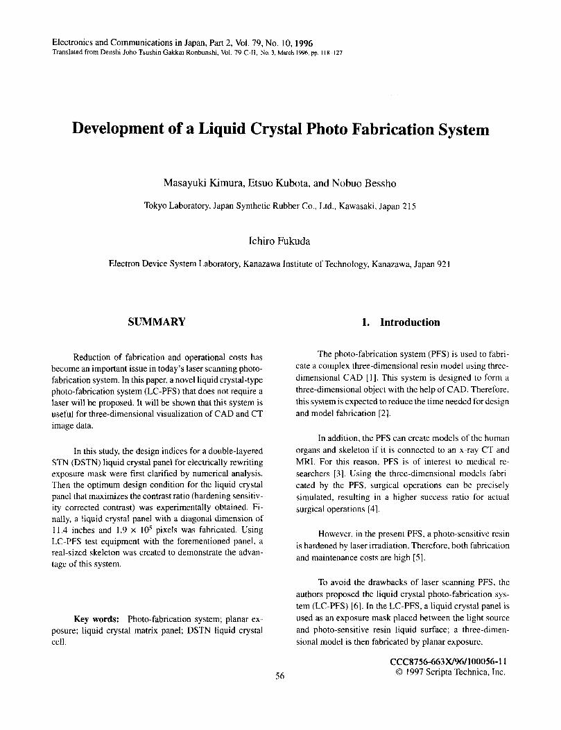
Figure 1 shows a conventional PFS with a laser, which is composed of a computer, laser beam irradiator, X-Y scanning of a laser system, elevator of a fabrication support and UV-resin [7]. Using a computer, 3-D informa-
(a) Configuration
Laser beam -
First layer Second layer Nth layer Complete
(b) Principle of Photo-fabrication
Fig. 1. Photo-fabrication system using laser.
I U L Computer
Work - UV Resin
Elevator
Bath Stage
I I
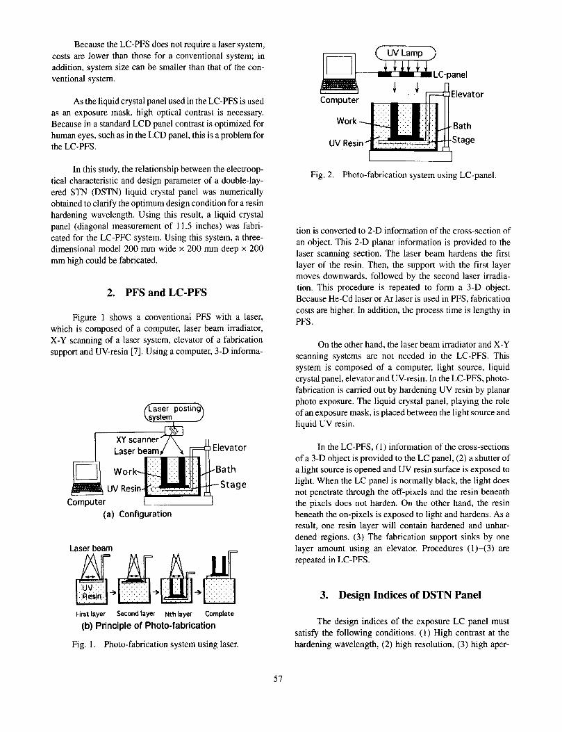
Fig. 2. Photo-fabrication system using LC-panel.
tion is converted to 2-D information of the cross-section of an object. This 2-D planar information is provided to the laser scanning section. The laser beam hardens the first layer of the resin. Then, the support with the first layer moves downwards, followed by the second laser irradia- tion. This procedure is repeated to form a 3-D object. Because He-Cd laser or Ar laser is used in PFS, fabrication costs are higher. In addition, the process time is lengthy in PFS .
On the other hand, the laser beam irradiator and X-Y scanning systems are not needed in the LC-PFS. This system is composed of a computer, light source, liquid crystal panel, elevator and UV-resin. In the LC-PFS, photo- fabrication is camed out by hardening UV resin by planar photo exposure. The liquid crystal panel, playing the role of an exposure mask, is placed between the light source and liquid UV resin.
In the LC-PFS, (1) information of the cross-sections of a 3-D object is provided to the LC panel, ( 2 ) a shutter of a light source is opened and UV resin surface is exposed to light. When the LC panel is normally black, the light does not penetrate through the off-pixels and the resin beneath the pixels does not harden. On the other hand, the resin beneath the on-pixels is exposed to light and hardens. As a result, one resin layer will contain hardened and unhar- dened regions. (3) The fabrication support sinks by one layer amount using an elevator. Procedures (1)-(3) are repeated in LC-PFS.
3. Design Indices of DSTN Panel
The design indices of the exposure LC panel must satisfy the following conditions. (1) High contrast at the hardening wavelength, (2) high resolution, (3) high aper-
57
ture ratio and point of fabrication time reduction, (4) high Table 1. Typical values for parameters used in calcula-
Parameter ~____._ __
Azimuth of Polarizer P Weg.1 Retardation of Driving ( A n . d ) D b m ]
Retardation of ( A n . d ) c @ m ] Cell
ComDensating Cell
transmittance at the hardening wavelength. In this study, to reduce fabrication costs, a passive matrix system was adopted. The normally blackmode DSTN system was adopted not only because it is advantageous in terms of condition (l), but also because it could be advantageous in terms of conditions (2) and (3) if the cell structure is correctly modified [8]. In addition, optimization was car- ried out using numerical analysis to satisfy condition (4).
Variation Range
0- -90 0.4-1.2
0.4-1.2
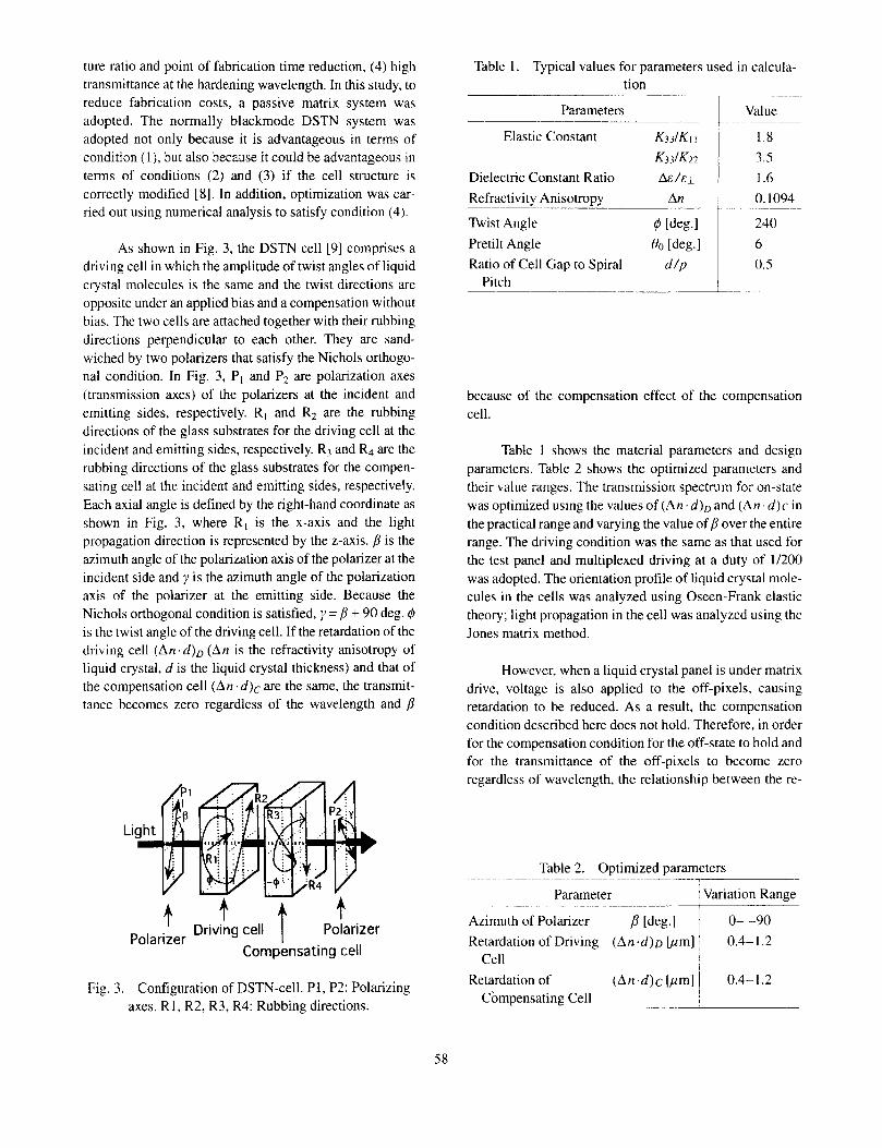
As shown in Fig. 3, the DSTN cell [9] comprises a driving cell in which the amplitude of twist angles of liquid crystal molecules is the same and the twist directions are opposite under an applied bias and a compensation without bias. The two cells are attached together with their rubbing directions perpendicular to each other. They are sand- wiched by two polarizers that satisfy the Nichols orthogo- nal condition. In Fig. 3, PI and P2 are polarization axes (transmission axes) of the polarizers at the incident and emitting sides, respectively. R, and R2 are the rubbing directions of the glass substrates for the driving cell at the incident and emitting sides, respectively. R7 and R4 are the rubbing directions of the glass substrates for the compen- sating cell at the incident and emitting sides, respectively. Each axial angle is defined by the right-hand coordinate as shown in Fig. 3, where R, is the x-axis and the light propagation direction is represented by the z-axis. p is the azimuth angle of the polarization axis of the polarizer at the incident side and y is the azimuth angle of the polarization axis of the polarizer at the emitting side. Because the Nichols orthogonal condition is satisfied, y = /? + 90 deg. $J is the twist angle of the driving cell. If the retardation of the driving cell ( A t ~ . d ) ~ (An is the refractivity anisotropy of liquid crystal, d is the liquid crystal thickness) and that of the compensation cell ( A n . d ) c are the same, the transmit- tance becomes zero regardless of the wavelength and p
Li
Fig.
Driving cell I Polarizer I
Polarizer Compensating cell
3 . Configuration of DSTN-cell. P1, P2: Polarizing axes. R1, R2, R3, R4: Rubbing directions.
- tion
Parameters
Elastic Constant K d K i I
K d K z Dielectric Constant Ratio A E / E I Refractivity Anisotropy An
Twist Angle 4 fdeg.1 Pretilt Angle 00 [deg.l Ratio of Cell Gap to Spiral d / P
Pitch
Value
1.8 3.5 1.6 0.1094
240 6 0.5
because of the compensation effect of the compensation cell.
Table 1 shows the material parameters and design parameters. Table 2 shows the optimized parameters and their value ranges. The transmission spectrum for on-state was optimized using the values of ( A n . d ) , and ( A n . d ) c in the practical range and varying the value ofp over the entire range. The driving condition was the same as that used for the test panel and multiplexed driving at a duty of 1/200 was adopted. The orientation profile of liquid crystal mole- cules in the cells was analyzed using Oseen-Frank elastic theory; light propagation in the cell was analyzed using the Jones matrix method.
However, when a liquid crystal panel is under matrix drive, voltage is also applied to the off-pixels, causing retardation to be reduced. As a result, the Compensation condition described here does not hold. Therefore, in order for the compensation condition for the off-state to hold and for the transmittance of the off-pixels to become zero regardless of wavelength, the relationship between the re-
Table 2. Optimized parameters
58
0.5 1 .o (An*d)D [vml
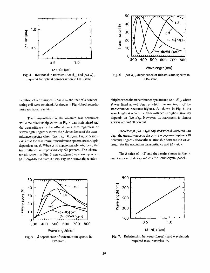
Fig. 4. Relationship between ( A n . d ) ~ and ( A r 1 . 4 ~ required for optical compensation in OFF-state.
tardation of a driving cell and that of a compen- sating cell were obtained. As shown in Fig. 4, both retarda- tions are linearly related.
The transmittance in the on-state was optimized while the relationship shown in Fig. 4 was maintained and the transmittance in the off-state was zero regardless of wavelength. Figure 5 shows the p dependence of the trans- mittance spectra when ( A r ~ . d ) ~ = 0.8pm. Figure 5 indi- cates that the maximum transmittance spectra are strongly dependent on /?. When /? is approximately -40 deg., the transmittance is approximately 50 percent. The charac- teristic shown in Fig. 5 was confirmed to show up when ( A n . d D differed from 0.8pm. Figure 6 shows the relation-
n
;F u C 0 v) v)
S
.-
.- L v) K m
50
40
30
20
10
0
,/I ry I I I 1 I 1 1 1 I I I I I I 1
300 400 500 600 700 800
- s Y
C 0 v) v)
v) C
.-
.- E
EJ I-
Fig. 6.
50
40
30
20
10
Wavelength[ nm] ( A r ~ . d ) ~ dependence of transmission spectra in
ON-state.
ship between the transmittance spectra and (An. d ) D , where p was fixed at -42 deg., at which the maximum of the transmittance becomes highest. As shown in Fig. 6, the wavelength at which the transmittance is highest strongly depends on ( A r ~ . d ) ~ . However, its maximum is almost always around 50 percent.
Therefore, if (An. d ) D is adjusted whena is around -40 deg., the transmittance in the on-state becomes highest (50 percent). Figure 7 shows the relationship between the wave- length for the maximum transmittance and ( A r 1 . 4 ~ .
The /? value of -42" and the results shown in Figs. 4 and 7 are useful design indices for liquid crystal panel.
0.5 1 .o Wavelength[ nm] ( A n - d b Cvml
Fig. 5 . /? dependence of transmission spectra in Fig. 7. Relationship between ( A n . d ) , and wavelength ON-state. required max transmission.
59
4. Optimization of Practical Liquid Crystal Panel
The described design indices provide important in- formation in designing a practical liquid crystal panel. At the same time, the spectral hardening sensitivity charac- teristic of UV resin, optical characteristics of polarizers, spectral distribution of light source and wavelength de- pendence of refractivity anisotropy of liquid crystal (wave- length dispersion) must be taken into account in designing a practical liquid crystal panel. The design condition of a liquid crystal panel will be optimized.
4.1. Spectral hardening sensitivity of resin
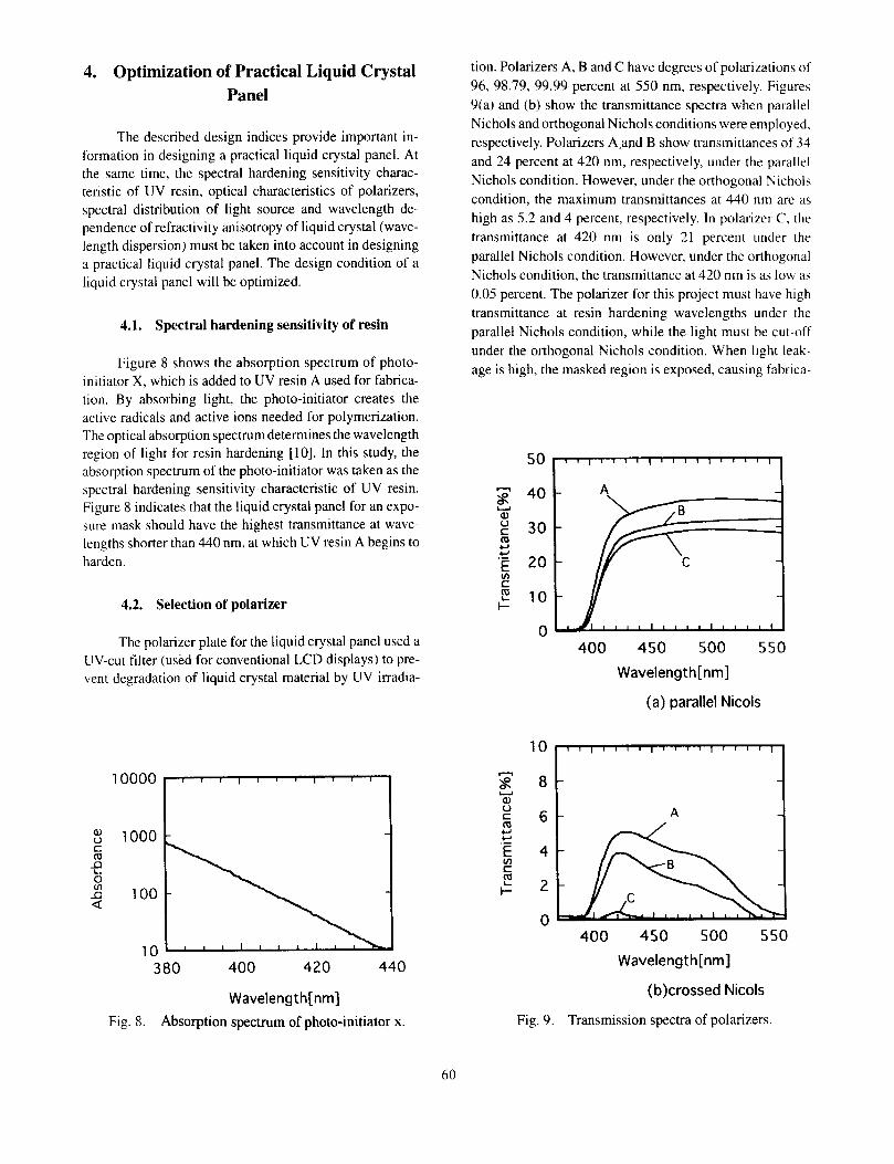
Figure 8 shows the absorption spectrum of photo- initiator X, which is added to UV resin A used for fabrica- tion. By absorbing light, the photo-initiator creates the active radicals and active ions needed for polymerization. The optical absorption spectrum determines the wavelength region of light for resin hardening [lo]. In this study, the absorption spectrum of the photo-initiator was taken as the spectral hardening sensitivity characteristic of UV resin. Figure 8 indicates that the liquid crystal panel for an expo- sure mask should have the highest transmittance at wave- lengths shorter than 440 nm, at which UV resin A begins to harden.
4.2. Selection of polarizer
tion. Polarizers A, B and C have degrees of polarizations of 96, 98.79, 99.99 percent at 550 nm, respectively. Figures 9(a) and (b) show the transmittance spectra when parallel Nichols and orthogonal Nichols conditions were employed. respectively. Polarizers A.and B show transmittances of 34 and 24 percent at 420 nm, respectively, under the parallel Nichols condition. However, under the orthogonal Nichols condition, the maximum transmittances at 440 nm are as high as 5.2 and 4 percent, respectively. In polarizcr C. the transmittance at 420 nm is only 21 percent under the parallel Nichols condition. However, under the orthogonal Nichols condition, the transmittance at 420 nm is as low as 0.05 percent. The polarizer for this project must have high transmittance at resin hardening wavelengths undcr the parallel Nichols condition, while the light must be cut-off under the orthogonal Nichols condition. When light leak- age is high, the masked region is exposed, causing fabrica-
40
30 u aJ
m U U
v) C
I-
‘E 20
2 10
The polarizer plate for the liquid crystal panel used a UV-cut filter (used for conventional LCD displays) to pre- vent degradation of liquid crystal material by UV irrddia-
I 10000
.- E
E v) c
l-
3 80 400 420 440
Wavelength[ nm] Absorption spectrum of photo-initiator x. Fig. 8.
0 400 450 500 550
Wavelength[ nm]
(a) parallel Nicols
l o k 8 t 1 6 - A
400 450 500 550 Wavelength[nm]
(b)crossed Nicols
Fig. 9. Transmission spectra of polarizers.
60
tion accuracy to degrade. In this study, polarizer C with a 99.9 percent degree of polarizer was used. The effective wavelength is between 380 nm (the shortest wavelength passing through polarizer C) and 440 nm (the point at which the photo-initiator begins to absorb light). In fabri- cation of the liquid crystal panel, the electrooptical property of the panel must be optimized in the effective resin hard- ening wavelength region.
4.3. Optimum design of liquid crystal panel
The quality of the liquid crystal panel for a photo-fab- rication exposure mask must be evaluated by transmittance and contrast, taking into account the photo-hardening sen- sitivity of resin. If T ( i ) is the spectral transmittance of the panel, P(A) is the spectral intensity of the light source and y ( 2 ) is the spectral absorption (spectral hardening sensitiv- ity) of resin, the panel transmittance corrected Tp by y ( 2 ) (hardening sensitivity corrected transmittance) is given by:
(1) 380 TP= 440
j 3 * m P ( A ) d A
The panel contrast corrected by y ( i ) , CRp (hardening sen- sitivity corrected contrast) is given by the ratio of the transmittance given by Eq. (1) in the on-state, Tp(on) and the transmittance in the off-state, Tp(off) .
(2)
By replacing y ( 2 ) given in Eq. (1) with the visibility sensi- tivity curve, the integration range is assumed to be the
CRp = Tp (on)/T, (off)
400 500 600
Wavelength[ nm]
Fig. 10. Wavelength dependence of refractive index An for liquid crystal material.
visible region. Then, Tp and CRp are identical with trans- mittance and contrast of a traditional display in the visible region, respectively.
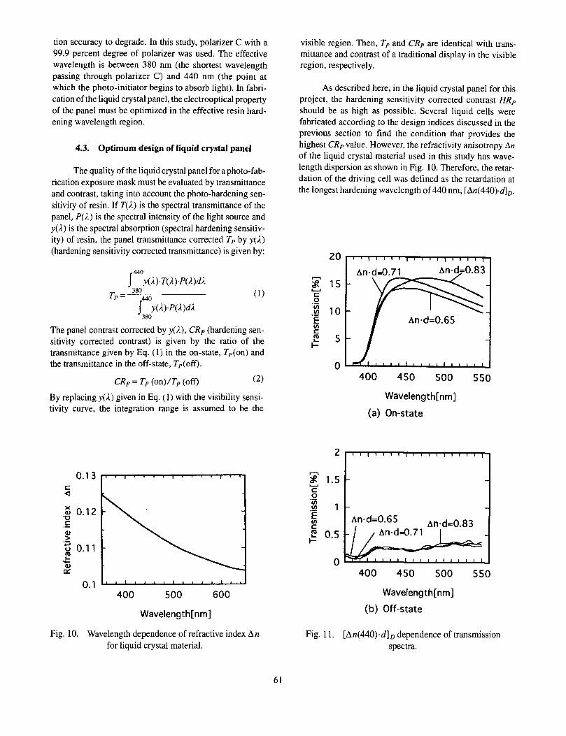
As described here, in the liquid crystal panel for this project, the hardening sensitivity corrected contrast HRp should be as high as possible. Several liquid cells were fabricated according to the design indices discussed in the previous section to find the condition that provides the highest CRp value. However, the refractivity anisotropy An of the liquid crystal material used in this study has wave- length dispersion as shown in Fig. 10. Therefore, the retar- dation of the driving cell was defined as the retardation at the longest hardening wavelength of 440 nm, [A~z(440).6]~.
n
;R Y
S 0 In In
In S
.-
.- E
2 I-
15
10
5
0 400 450 500 550
Wavelength[ nm]
(a) On-state
n ;R 1.5 U c 0 .- .- $ 1 E
i! 0.5
0
v) c I-
t An-d=0.83 An.d=0.65
400 450 500 550
Wavelength [nm]
(b) Off-state
Fig. 11. [An(440).dlD dependence of transmission spectra.
61
Y h 0.6
~ ~~~~~~~~
LC mode
Table 3. Hardening sensitivity corrected contrast
Cell 1 Cell 2 Cell 3
4 0 ; Corrected Sensitivity 0.83 30
~~ No. of pixels Display area Dot size Dot pitch Duty cycle
.. ~ ~~- ~~
~~~ _____ _____.___
0 300 350 400 450 500 550 600
Wavelength[ nm]
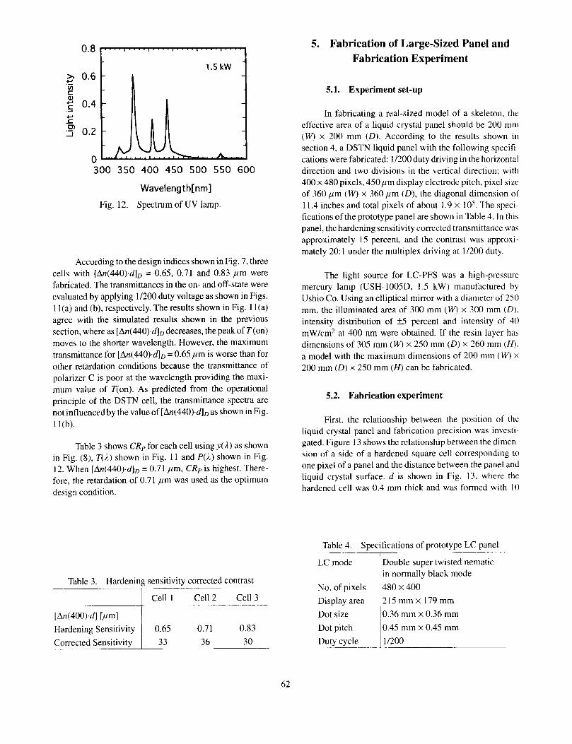
Fig. 12. Spectrum of U V lamp.
Double super twisted nematic in normally black mode 480 x 400 2 I5 mm x 179 mm 0.36 mm x 0.36 mm 0.45 mm x 0.45 mm 1/200
According to the design indices shown in Fig. 7, three cells with [An(440).61D = 0.65, 0.71 and 0.83 p m were fabricated. The transmittances in the on- and off-state were evaluated by applying 1/200 duty voltage as shown in Figs. 1 1 (a) and (b), respectively. The results shown in Fig. 1 1 (a) agree with the simulated results shown in the previous section, where as [An(440)& decreases, the peak of T(on) moves to the shorter wavelength. However, the maximum transmittance for [An(440).dD = 0.65 pm is worse than for other retardation conditions because the transmittance of polarizer C is poor at the wavelength providing the rnaxi- mum value of T(on). As predicted from the operational principle of the DSTN cell, the transmittance spectra are not influenced by the value of [h(440).dlD as shown in Fig. 1 l(b).
Table 3 shows CRp for each cell using y(1) as shown in Fig. (8), T ( 2 ) shown in Fig. 11 and P(A) shown in Fig. 12. When [An(440)& = 0.7 1 pm, CRp is highest. There- fore, the retardation of 0.71 p m was used as the optimum design condition.
5. Fabrication of Large-Sized Panel and Fabrication Experiment
5.1. Experiment set-up
In fabricating a real-sized model of a skeleton, the effective area of a liquid crystal panel should be 200 mm (w) x 200 mm (D). According to the results shown in section 4, a DSTN liquid panel with the following specifi- cations were fabricated: 1/200duty driving in the horizontal direction and two divisions in the vertical direction; with 400 x 480 pixels, 450pm display electrode pitch, pixel sire of 360 p m ( W) x 360 prn ( D ) , the diagonal dimension of I 1.4 inches and total pixels of about 1.9 x los. The speci- fications of the prototype panel are shown in Table 4. In this panel, the hardening sensitivity corrected transmittance was approximately 15 percent, and the contrast was approxi- mately 20: I under the multiplex driving at 1 /200 duty.
The light source for LC-PFS was a high-pressure mercury lamp (USH-I005D, 1.5 kW) manufactured by Ushio Co. Using an elliptical mirror with a diameter of 250 mm, the illuminated area of 300 mm (W) x 300 mm (D ) , intensity distribution of +5 percent and intensity of 40 mW/cm2 at 400 nm were obtained. If the resin layer has dimensions of 305 mm (w) x 250 mm ( D ) x 260 mm (K). a model with the maximum dimensions of 200 mni ( W ) x 200 mm (D) x 250 mm (H) can be fabricated.
5.2. Fabrication experiment
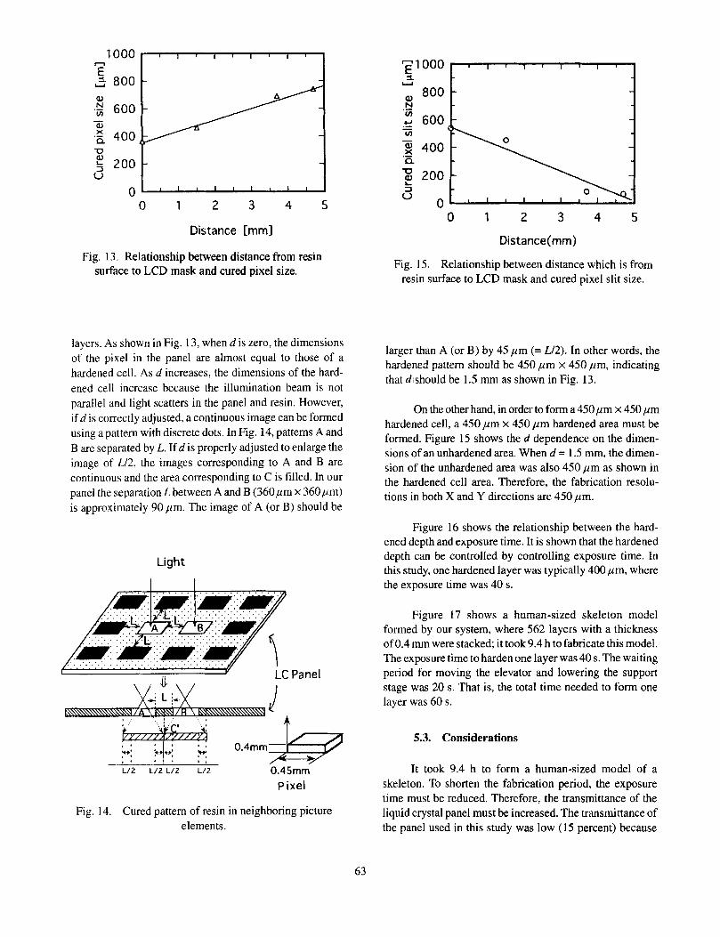
First, the relationship between the position of the liquid crystal panel and fabrication precision was investi- gated. Figure 13 shows the relationship between the dirnen- sion of a side of a hardened square cell corresponding to one pixel of a panel and the distance between the panel and liquid crystal surface. d is shown in Fig. 13, where the hardened cell was 0.4 mm thick and was formed with I0
62
- 1 000 5
, I
,-: , , _ _ _
U
a 0.4mm- d o
:-+ y . I I I
n E 2 800 a, .: 600 - a, .g 400 U g 200 V
0 0 1 2 3 4 5
Distance [mml
Fig. 13. Relationship between distance from resin surface to LCD mask and cured pixel size.
layers. As shown in Fig. 13, when d is zero, the dimensions of the pixel in the panel are almost equal to those of a hardened cell. As d increases, the dimensions of the hard- ened cell increase because the illumination beam is not parallel and light scatters in the panel and resin. However, if d is correctly adjusted, a continuous image can be formed using a pattern with discrete dots. In Fig. 14, patterns A and B are separated by L. If d is properly adjusted to enlarge the image of Ll2, the images corresponding to A and B are continuous and the area corresponding to C is filled. In our panel the separation L between A and B (360pm x 360pm) is approximately 90 pm. The image of A (or B) should be
Light
800
.- 600
al N .-
- u)
H 200
0 (3
0 1 2 3 4 5
Distance( mrn)
Fig. 15. Relationship between distance which is from resin surface to LCD mask and cured pixel slit size.
larger than A (or B) by 45 p m (= W2). In other words, the hardened pattern should be 450 pm x 450 pm, indicating that dishould be 1.5 mm as shown in Fig. 13.
On the other hand, in order to form a 450 p m x 450 p m hardened cell, a 450 pm x 450 p m hardened area must be formed. Figure 15 shows the d dependence on the dimen- sions of an unhardened area. When d = 1.5 mm, the dimen- sion of the unhardened area was also 450 p m as shown in the hardened cell area. Therefore, the fabrication resolu- tions in both X and Y directions are 450 pm.
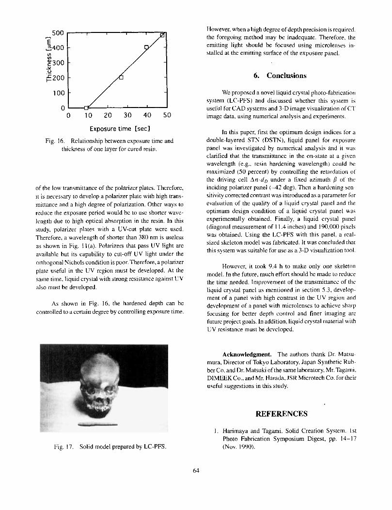
Figure 16 shows the relationship between the hard- ened depth and exposure time. It is shown that the hardened depth can be controlled by controlling exposure time. In this study, one hardened layer was typically 400pm, where the exposure time was 40 s.
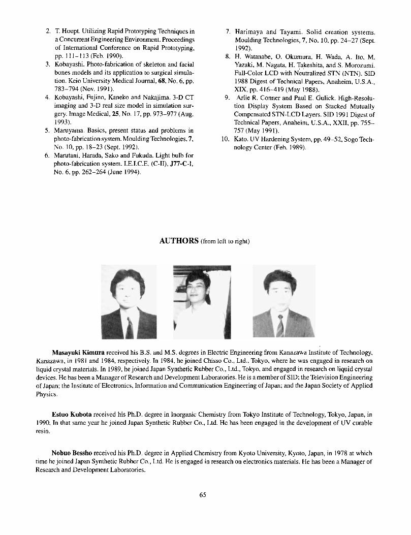
Figure 17 shows a human-sized skeleton model formed by our system, where 562 layers with a thickness of 0.4 mm were stacked; it took 9.4 h to fabricate this model. The exposure time to harden one layer was 40 s. The waiting
I/ period for moving the elevator and lowering the support
\ I + \ / I
d stage was 20 s. That is, the total time needed to form one layer was 60 s.
63
500 n
E 2 4 0 0 v) v)
Y u E 300
200
100
0 0 10 20 30 40 50
Exposure time [secl
Fig. 16. Relationship between exposure time and thickness of one layer for cured resin.
of the low transmittance of the Folarizer plates. Therefore, it is necessary to develop a polarizer plate with high trans- mittance and a high degree of polarization. Other ways to reduce the exposure period would be to use shorter wave- length due to high optical absorption in the resin. In this study, polarizer plates with a UV-cut plate were used. Therefore, a wavelength of shorter than 380 nm is useless as shown in Fig. 1 Ifa). Polarizers that pass UV light are available but its capability to cut-off UV light under the orthogonal Nichols condition is poor. Therefore, a polarizer plate useful in the UV region must be developed. At the same time, liquid crystal with strong resistance against U V also must be developed.
As shown in Fig. 16, the hardened depth can be controlled to a certain degree by controlling exposure time.
Fig. 17. Solid model prepared by LC-PFS.
However, when a high degree of depth precision is required, thc foregoing method may be inadequate. Therefore, the emitting light should be focused using microlenses in- stalled at the emitting surface of the exposure panel.
6. Conclusions
We proposed a novel liquid crystal photo-fabrication system (LC-PFS) and discussed whether this system is useful for CAD systems and 3-D image visualization of CT image data, using numerical analysis and experiments.
In this paper. first the optimum design indices for a double-layered STN (DSTN), liquid panel for exposure panel was investigated by numerical analysis and i t was clarified that the transmittance in the on-state at a given wavelength (e.g., resin hardening wavelength) could be maximized (50 percent) by controlling the retardation of the driving cell An.d l , under a fixed azimuth of the inciding polarizer panel (-42 deg). Then a hardening sen- sitivity corrected contrast was introduced as a parameter for evaluation of the quality of a liquid crystal panel and the optimum design condition of a liquid crystal panel was experimentally obtained. Finally, a liquid crystal panel (diagonal measurement of 1 1.4 inches) and 190,000 pixels was obtained. Using the LC-PFS with this panel, a real- sized skeleton model was fabricated. It was concluded that this system was suitable for use as a 3-D visualization tool.
However, it took 9.4 h to make only one skeleton model. In the future, much effort should be made to reduce the time needed. Improvement of the transmittance of the liquid crystal panel as mentioned in section 5.3, develop- ment of a panel with high contrast in the UV region and development of a panel with microlenses to achieve sharp focusing for better depth control and finer imaging are future project goals. In addition, liquid crystal material with UV resistance must be developed.
Acknowledgment. The authors thank Dr. Matsu- mura, Director of Tokyo Laboratory, Japan Synthetic Rub- ber Co. and Dr. Matsuki of the same laboratory, Mr. Tagami, DIMEEK Co., and Mr. Harada, JSR Microtech Co. for their useful suggestions in this study.
REFERENCES
1 . Harimaya and Tagami. Solid Creation System. 1st Photo Fabrication Symposium Digest, pp. 14- I 7 (Nov. 1990).
64
2. T. Houpt. Utilizing Rapid Prototyping Techniques in a Concurrent Engineering Environment. Proceedings of International Conference on Rapid Prototyping, pp. 1 11-1 13 (Feb. 1990).
3. Kobayashi. Photo-fabrication of skeleton and facial bones models and its application to surgical simula- tion. Keio University Medical Journal, 68, No. 6, pp.
4. Kobayashi, Fujino, Kaneko and Nakajima. 3-D CT imaging and 3-D real size model in simulation sur- gery. Image Medical, 25, No. 17, pp. 973-977 (Aug. 1993).
5. Maruyama. Basics, present status and problems in photo-fabrication system. Moulding Technologies, 7, No. 10, pp. 18-23 (Sept. 1992).
6. Marutani, Harada, Sako and Fukuda. Light bulb for photo-fabrication system. I.E.I.C.E. (C-II), J77-C-I, No. 6, pp. 262-264 (June 1994).
783-794 (Nov. 1991).
7. Harimaya and Tayami. Solid creation systems. Moulding Technologies, 7, No. 10, pp. 24-27 (Sept. 1992).
8. H. Watanabe, 0. Okumura, H. Wada, A. Ito, M. Yazaki, M. Nagata, H. Takeshita, and S. Morozumi. Full-Color LCD with Neutralized STN (NTN). SID 1988 Digest of Technical Papers, Anaheim, U.S.A., XIX, pp. 416-419 (May 1988).
9. Arlie R. Conner and Paul E. Gulick. High-Resolu- tion Display System Based on Stacked Mutually Compensated STN-LCD Layers. SID 1991 Digest of Technical Papers, Anaheim, U.S.A., XXII, pp. 755- 757 (May 1991).
10. Kato. UV Hardening System, pp. 49-52, Sogo Tech- nology Center (Feb. 1989).
AUTHORS (from left to right)
Masayuki Kimura received his B.S. and M.S. degrees in Electric Engineering from Kanazawa Institute of Technology, Kanazawa, in 1981 and 1984, respectively. In 1984, he joined Chisso Co., Ltd., Tokyo, where he was engaged in research on liquid crystal materials. In 1989, he joined Japan Synthetic Rubber Co., Ltd., Tokyo, and engaged in research on liquid crystal devices. He has been a Manager of Research and Development Laboratories. He is a member of SID; the Television Engineering of Japan; the Institute of Electronics, Information and Communication Engineering of Japan; and the Japan Society of Applied Physics.
Estuo Kubota received his Ph.D. degree in Inorganic Chemistry from Tokyo Institute of Technology, Tokyo, Japan, in 1990. In that same year he joined Japan Synthetic Rubber Co., Ltd. He has been engaged in the development of UV curable resin.
Nobuo Bessho received his Ph.D. degree in Applied Chemistry from Kyoto University, Kyoto, Japan, in 1978 at which time he joined Japan Synthetic Rubber Co., Ltd. He is engaged in research on electronics materials. He has been a Manager of Research and Development Laboratories.
65
AUTHOR
Ichiro Fukuda received his B.S., M.S. and Ph.D. degrees in Electronic Engineering from Tohoku University, Sendai, Japan, in 1965, 1967 and 1981, respectively. In 1967, he joined Mitsumi Denki Corporation, Tokyo, where he was engaged in research on thin-film devices. In 1970, he joined Kanazawa Institute of Technology and engaged in research on thin-film devices and liquid crystal devices. He has been a Professor on the Faculty of Engineering, Kanazawa Institute of Technology, since 1983. He is a member of SID; the Television Engineering of Japan; the Institute of Electronics, Information and Communication Engineering of Japan; and the Japan Society of Applied Physics.
66