Embed Size (px)
Citation preview
Development Of
Characteristic Impedance Meter M. Sivaramakrishna,
Indira Gandhi Centre for Atomic Research,
Department of Atomic Enrgy, Kalpakkam, Tamilnadu, India
Abstract – The paper describes the development of
characteristic impedance meter. This is the first step towards
automization of measurement of characteristic impedance of high
frequency signal cables and connectors in Fast breeder reactors.
Index Terms—Cable, impedance, connector. For a list of
suggested keywords, send a blank e-mail to
1. INTRODUCTION
The paper is on the “DEVELOMENT OF
CHARACTERISTIC IMPEDANCE METER”. The work is to
design the scheme & circuit for the meter and program it to
display the characteristic impedance value of the cable
connected to the terminals of the meter, especially in the light
of non availability of meter for direct measurement of
characteristic impedance of cables. Circuit is designed keeping
in view of various options the user should be provided, like
reset, test mode, voltage and frequency selection range etc.
The paper details the simulation studies. A prototype is being
developed based on the study.
1.1 SIGNIFICANCE OF CHARACTERISTIC IMPEDANCE
OF A CABLE:
Signal transmission at high frequencies is lot different to that
at low frequencies.
The voltage at each point in a low frequency signal carrying
wire can be considered to be constant and the resistance to be
zero. In case of high frequency signal transmission, the wave
nature of the signal is to be considered. Any media that
supports high frequency signal transmission has characteristic
impedance associated with it. Improper termination of such
high frequency signal carrying cable causes reflections.
These reflections are due to mismatch of impedance between
the cable and the terminal and results in signal distortion. A
parallel resistance equal to the characteristic impedance of the
cable when connected at the termination of the cable can
reduce the reflections to a great extent, almost to zero.
The characteristic impedance, Z0, of a line is the input
impedance of an infinite length of the line. Characteristic
impedance is of prime importance for good transmission. For
a cable with constant impedance the signal gets transmitted as
it is, without any distortion. If the impedance value of the
cable keeps varying, energy is reflected back and the signal
gets distorted. For optimal signal quality, the goal is to keep
the impedance of the cable constant as seen by the signal.
Maximum power transfer occurs when the source has the same
impedance as the load. Thus for sending signals over a line,
the transmitting equipment must have the same characteristic
impedance as the line to get the maximum signal into the line.
At the other end of the line, the receiving equipment must also
have the same impedance as the line to be able to get the
maximum signal out of the line. Where impedances do not
match, some of the signal is reflected back towards the source.
In many cases this reflected signal causes problems and is
therefore undesirable.
Whereas, if the cable is terminated in its matching
characteristic impedance, it cannot be observed if the cable is
infinitely long, the entire signal that is fed into the cable is
taken by the cable and the load.
1.2 NEED FOR THE METER:
The high frequency signals can be of very low magnitude like
the signals produced by the sensors that are used to monitor
the reactor functioning. The cables delivering such signals
must be properly terminated to avoid loss of information.
Using the meter, the characteristic impedance of the cable can
be found out. By knowing the characteristic impedance value
from the meter, the cable can be checked if it is properly
terminated or not. The meter will be very handy especially
when dealing with no. of field cables.
1.3 METER DEVELOPMENT:
Maximum power transmission principle is used to develop the
meter. The power delivered by the cable is maximum when
the cable is connected to a resistance equal to the cable‟s
characteristic impedance value. A voltage controlled resistor is
used in the circuit, whose value is varied until maximum
power transmission is achieved and the corresponding
resistance value is displayed as characteristic impedance value
of the cable. A microcontroller is used to calculate the power
transmitted and to control the other peripheral devices like
LCD, DAC and ADC. Annexure 1 gives the details of
characteristic impedance in general industrial applications.
2. CHARACTRISTIC IMPEDANCE VALUES:
The earliest viable long-distance electrical communications
system was the telegraph and its introduction spawned a whole
range of new studies, techniques and products intended to
547
International Journal of Engineering Research & Technology (IJERT)
Vol. 2 Issue 5, May - 2013ISSN: 2278-0181
www.ijert.org
IJERT
IJERT
maximize its benefits and its efficiency. Characteristic
impedance of the resulting transmission lines was 600 ohms.
The characteristic impedance of a wire-pair transmission line,
though a function of wire thickness, distance between the
conductors and the permittivity of the insulation between the
pair of wires, 600 ohms was widely adopted as the 'standard'
for telecommunications systems and later broadcast studio
installations. More modern multi-paired cables had
characteristic impedance closer to 140 ohms. Given that
characteristic-impedance only has significance where the
cable distances are a significant fraction of the wavelengths of
the signals being carried the cable runs in general didn't come
close to the distances where characteristic impedance is an
important factor. The introduction of digital technology,
however, revived the importance of characteristic impedance
as the cable now had to demonstrate a reliable and predictable
performance at frequencies significantly beyond their
analogue counterparts and are now operating with signal
wavelengths closer to the run-lengths of the cables. Presently,
75 ohms coaxial are widely available in the market. The
characteristic impedance of the cable often ranges from 50 to
300 ohms.
3. EXISTING METHODS FOR CHARACTERISTIC
IMPEDANCE CALCULATION:
3.1 CHARACTERISTIC IMPEDANCE EQUATION IN
DIFFERENT CASES:
In general, the characteristic impedance is a complex number
with a resistive and reactive component. It is a function of the
frequency of the applied signal, and is unrelated to length. At
very high frequencies, the characteristic impedance value
asymptotes to a fixed value which is resistive in nature. For
example, coaxial cables have an impedance of 50 or 75 Ohms
at high frequencies. Typically, twisted-pair telephone cables
have an impedance of 100 Ohms above 1 MHz .
Lossless transmission: When R and G are negligibly small the
transmission line is considered as a lossless structure. In this
hypothetical case, the model depends only on
the L and C elements which case the expression reduces to Z0
= sqrt (L/C
For materials commonly used for cable insulation, G is small
enough that it can be neglected when compared with 2ωC. At
low frequencies, 2ωL is so small compared with R that it can
be neglected. Therefore at low frequencies the following
equation can be used:
Z0=sqrt(R/2jωC
When ω is large enough, the two terms containing ω becomes
so large that R and G may be neglected and the resultant
equation is
Z0=sqrt (2jωL/2jωC) =sqrt (L/C)
3.2 DIFFERENT METHODS TO CALCULATE
CHARACTERISTIC IMPEDANCE VALUE:
a) High frequency measurements of Z0 can be made
by determining the velocity of propagation and
capacitance of the cable or by reflectometry.
b) For twisted pair and coaxial cables, the
resistance is determined by the diameter or
weight of copper, the inductance is very small,
and the shunt conductance is small. The major
influence on characteristic impedance and other
secondary coefficients is the capacitance. This is
largely determined by the type of insulation
(dielectric) used. Characteristic impedance, for
high frequencies, can be stated in terms of the
physical dimensions of the cable. These
formulae apply to copper conductor cables.
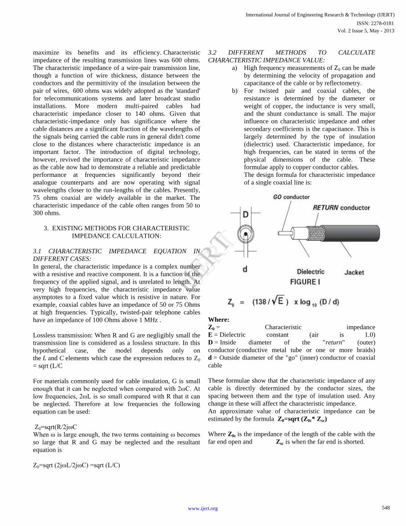
The design formula for characteristic impedance
of a single coaxial line is:
Where: Z0 = Characteristic impedance
E = Dielectric constant (air is 1.0)
D = Inside diameter of the "return" (outer)
conductor (conductive metal tube or one or more braids)
d = Outside diameter of the "go" (inner) conductor of coaxial
cable
These formulae show that the characteristic impedance of any
cable is directly determined by the conductor sizes, the
spacing between them and the type of insulation used. Any
change in these will affect the characteristic impedance.
An approximate value of characteristic impedance can be
estimated by the formula Z0=sqrt (Z0c* Zsc)
Where Z0c is the impedance of the length of the cable with the
far end open and Zsc is when the far end is shorted.
548
International Journal of Engineering Research & Technology (IJERT)
Vol. 2 Issue 5, May - 2013ISSN: 2278-0181
www.ijert.org
IJERT
IJERT
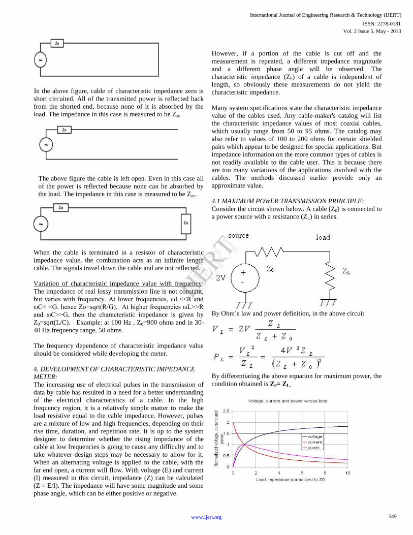
In the above figure, cable of characteristic impedance zero is
short circuited. All of the transmitted power is reflected back
from the shorted end, because none of it is absorbed by the
load. The impedance in this case is measured to be Zsc.
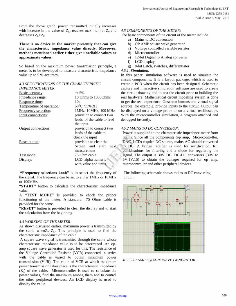
The above figure the cable is left open. Even in this case all
of the power is reflected because none can be absorbed by
the load. The impedance in this case is measured to be Zoc.
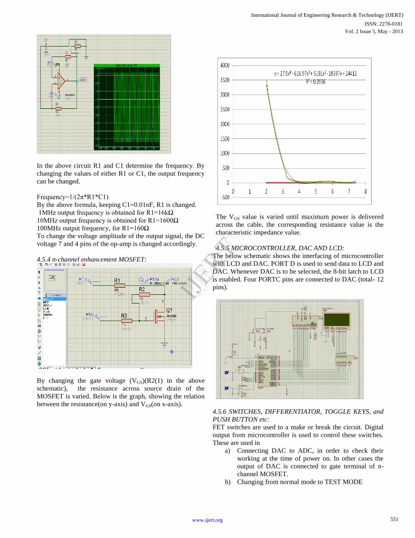
When the cable is terminated in a resistor of characteristic
impedance value, the combination acts as an infinite length
cable. The signals travel down the cable and are not reflected.
Variation of characteristic impedance value with frequency:
The impedance of real lossy transmission line is not constant,
but varies with frequency. At lower frequencies, ωL<<R and
ωC< <G. hence Zo=sqrt(R/G). At higher frequencies ωL>>R
and ωC>>G, then the characteristic impedance is given by
Z0=sqrt(L/C). Example: at 100 Hz , Z0=900 ohms and in 30-
40 Hz frequency range, 50 ohms.
The frequency dependence of characteristic impedance value
should be considered while developing the meter.
4. DEVELOPMENT OF CHARACTERISTIC IMPEDANCE
METER:
The increasing use of electrical pulses in the transmission of
data by cable has resulted in a need for a better understanding
of the electrical characteristics of a cable. In the high
frequency region, it is a relatively simple matter to make the
load resistive equal to the cable impedance. However, pulses
are a mixture of low and high frequencies, depending on their
rise time, duration, and repetition rate. It is up to the system
designer to determine whether the rising impedance of the
cable at low frequencies is going to cause any difficulty and to
take whatever design steps may be necessary to allow for it.
When an alternating voltage is applied to the cable, with the
far end open, a current will flow. With voltage (E) and current
(I) measured in this circuit, impedance (Z) can be calculated
(Z = E/I). The impedance will have some magnitude and some
phase angle, which can be either positive or negative.
However, if a portion of the cable is cut off and the
measurement is repeated, a different impedance magnitude
and a different phase angle will be observed. The
characteristic impedance (Z0) of a cable is independent of
length, so obviously these measurements do not yield the
characteristic impedance.
Many system specifications state the characteristic impedance
value of the cables used. Any cable-maker's catalog will list
the characteristic impedance values of most coaxial cables,
which usually range from 50 to 95 ohms. The catalog may
also refer to values of 100 to 200 ohms for certain shielded
pairs which appear to be designed for special applications. But
impedance information on the more common types of cables is
not readily available to the cable user. This is because there
are too many variations of the applications involved with the
cables. The methods discussed earlier provide only an
approximate value.
4.1 MAXIMUM POWER TRANSMISSION PRINCIPLE:
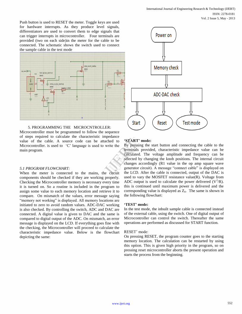
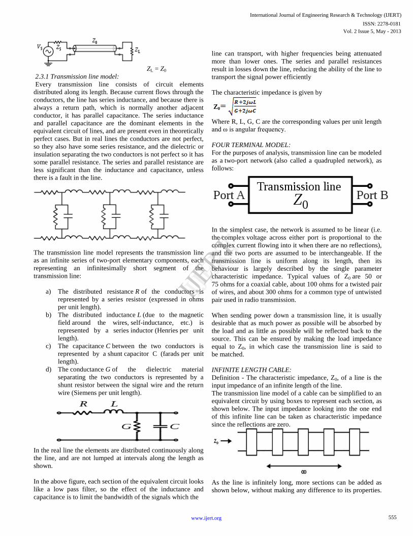
Consider the circuit shown below. A cable (Z0) is connected to
a power source with a resistance (ZL) in series.
By Ohm‟s law and power definition, in the above circuit
By differentiating the above equation for maximum power, the
condition obtained is Z0= ZL.
549
International Journal of Engineering Research & Technology (IJERT)
Vol. 2 Issue 5, May - 2013ISSN: 2278-0181
www.ijert.org
IJERT
IJERT
From the above graph, power transmitted initially increases
with increase in the value of ZL, reaches maximum at Z0 and
decreases ZL>Z0.
There is no device in the market presently that can give
the characteristic impedance value directly. Moreover,
methods mentioned earlier either give unreliable values or
approximate values.
So based on the maximum power transmission principle, a
meter is to be developed to measure characteristic impedance
value up to 5 % accuracy.
4.3 SPECIFICATIONS OF THE CHARACTERISTIC
IMPEDANCE METER:
Basic accuracy: +/-5%
Impedance range: 10 Ohms to 1000Ohms
Response time: 10s
Temperature of operation: 500C, 95%RH
Frequency selection: 1MHz, 10MHz, 100 MHz
Input connections: provision to connect two
leads of the cable to feed
the input
Output connections: provision to connect two
leads of the cable to
check the input
Reset button: provision to clear the
Screen and start next
measurement
Test mode: 75 Ohm cable
Display: LCD, alpha numeric
with value and units,
“Frequency selections knob” is to select the frequency of
the signal. The frequency can be set to either 1MHz or 10MHz
or 100MHz.
“START” button to calculate the characteristic impedance
value.
A “TEST MODE” is provided to check the proper
functioning of the meter. A standard 75 Ohms cable is
provided for the same.
“RESET” button is provided to clear the display and to start
the calculation from the beginning.
4.4 WORKING OF THE METER:
As shown discussed earlier, maximum power is transmitted by
the cable whenZ0=ZL. This principle is used to find the
characteristic impedance of the cable.
A square wave signal is transmitted through the cable whose
characteristic impedance value is to be determined. An op-
amp square wave generator is used for this. The resistance of
the Voltage Controlled Resistor (VCR) connected in series
with the cable is varied to obtain maximum power
transmission (V2/R). The value of VCR at which maximum
power transmission takes place is the characteristic impedance
(Z0) of the cable. Microcontroller is used to calculate the
power values, find the maximum among them and to control
the other peripheral devices. An LCD display is used to
display the value.
4.5 COMPONENTS OF THE METER:
The basic components of the circuit of the meter include
a) Mains to DC conversion
b) OP AMP square wave generator
c) Voltage controlled variable resistor
d) Microcontroller
e) 12-bit Digital to Analog converter
f) LCD display
g) 8-bit Latch, switches, differentiator
4.5.1. Simulation:
In this paper, simulation software is used to simulate the
circuit components. It is a layout package, which is used to
create a PCB when the circuit has been designed. Schematic
capture and interactive simulation software are used to create
the circuit drawing and to test the circuit prior to building the
real hardware. Mathematical circuit modeling system is done
to get the real experience. Onscreen buttons and virtual signal
sources, for example, provide inputs to the circuit. Output can
be displayed on a voltage probe or on a virtual oscilloscope.
With the microcontroller simulation, a program attached and
debugged instantly.
4.5.2 MAINS TO DC CONVERSION:
Power is supplied to the characteristic impedance meter from
mains. Since all the components (op amp, Microcontroller,
DAC, LCD) require DC source, mains AC should converted
to DC. A bridge rectifier is used for rectification, RC
combinations for filtering and a diode for regulating the
signal. The output is 30V DC. DC-DC converters (30V to
5V,1V,15) to obtain the voltages required for op amp,
microcontroller and other peripheral devices.
The following schematic shows mains to DC converting
circuit:
4.5.3 OP AMP SQUARE WAVE GENERATOR:
550
International Journal of Engineering Research & Technology (IJERT)
Vol. 2 Issue 5, May - 2013ISSN: 2278-0181
www.ijert.org
IJERT
IJERT
In the above circuit R1 and C1 determine the frequency. By
changing the values of either R1 or C1, the output frequency
can be changed.
Frequency=1/(2π*R1*C1)
By the above formula, keeping C1=0.01nF, R1 is changed.
1MHz output frequency is obtained for R1=16kΩ
10MHz output frequency is obtained for R1=1600Ω
100MHz output frequency, for R1=160Ω
To change the voltage amplitude of the output signal, the DC
voltage 7 and 4 pins of the op-amp is changed accordingly.
4.5.4 n-channel enhancement MOSFET:
By changing the gate voltage (VGS)(R2(1) in the above
schematic), the resistance across source drain of the
MOSFET is varied. Below is the graph, showing the relation
between the resistance(on y-axis) and VGS(on x-axis).
The VGS value is varied until maximum power is delivered
across the cable, the corresponding resistance value is the
characteristic impedance value.
4.5.5 MICROCONTROLLER, DAC AND LCD:
The below schematic shows the interfacing of microcontroller
with LCD and DAC. PORT D is used to send data to LCD and
DAC. Whenever DAC is to be selected, the 8-bit latch to LCD
is enabled. Four PORTC pins are connected to DAC (total- 12
pins).
4.5.6 SWITCHES, DIFFERENTIATOR, TOGGLE KEYS, and
PUSH BUTTON etc:
FET switches are used to a make or break the circuit. Digital
output from microcontroller is used to control these switches.
These are used in
a) Connecting DAC to ADC, in order to check their
working at the time of power on. In other cases the
output of DAC is connected to gate terminal of n-
channel MOSFET.
b) Changing from normal mode to TEST MODE
551
International Journal of Engineering Research & Technology (IJERT)
Vol. 2 Issue 5, May - 2013ISSN: 2278-0181
www.ijert.org
IJERT
IJERT
Push button is used to RESET the meter. Toggle keys are used
for hardware interrupts. As they produce level signals,
differentiators are used to convert them to edge signals that
can trigger interrupts in microcontroller. Four terminals are
provided (two on each side)in the meter for the cable to be
connected. The schematic shows the switch used to connect
the sample cable in the test mode
5. PROGRAMMING THE MICROCNTROLLER:
Microcontroller must be programmed to follow the sequence
of steps required to calculate the characteristic impedance
value of the cable. A source code can be attached to
Microcontroller. is used to „C‟ language is used to write the
main program.
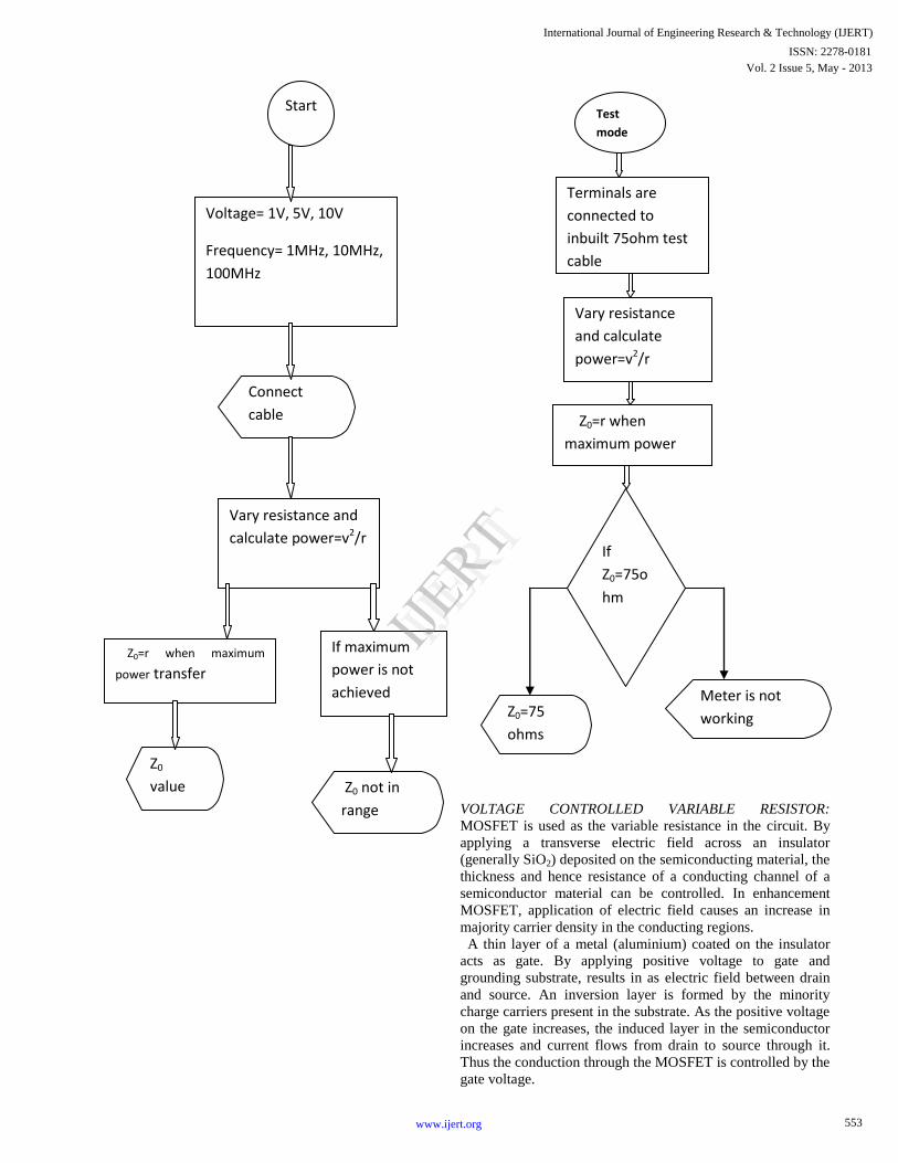
5.1 PROGRAM FLOWCHART:
When the meter is connected to the mains, the circuit
components should be checked if they are working properly.
Checking the Microcontroller memory is necessary every time
it is turned on. So a routine is included in the program to
assign some value to each memory location and retrieve it to
compare. On mismatch of the values, error message saying
“memory not working” is displayed. All memory locations are
initiated to zero to avoid random values. ADC-DAC working
is also checked. By controlling the switch, ADC and DAC are
connected. A digital value is given to DAC and the same is
compared to digital output of the ADC. On mismatch, an error
message is displayed on the LCD. If everything goes fine with
the checking, the Microcontroller will proceed to calculate the
characteristic impedance value. Below is the flowchart
depicting the same:
„START‟ mode: By pressing the start button and connecting the cable to the
terminals provided, characteristic impedance value can be
calculated. The voltage amplitude and frequency can be
selected by changing the knob positions. The internal circuit
changes accordingly (R1 value in the op amp square wave
generator circuit). A message “connect cable” is displayed on
the LCD. After the cable is connected, output of the DAC is
used to vary the MOSFET resistance value(R). Voltage from
ADC output is used to calculate the power delivered (V2/R).
this is continued until maximum power is delivered and the
corresponding value is displayed as Z0. The same is shown in
the following flowchart:
„TEST‟ mode:
In the test mode, the inbuilt sample cable is connected instead
of the external cable, using the switch. One of digital output of
Microcontroller can control the switch. Thereafter the same
operations are performed as discussed for START function.
RESET‟ mode:
On pressing RESET, the program counter goes to the starting
memory location. The calculation can be restarted by using
this option. This is given high priority in the program, so on
pressing reset microcontroller aborts the present operation and
starts the process from the beginning.
552
International Journal of Engineering Research & Technology (IJERT)
Vol. 2 Issue 5, May - 2013ISSN: 2278-0181
www.ijert.org
IJERT
IJERT
VOLTAGE CONTROLLED VARIABLE RESISTOR:
MOSFET is used as the variable resistance in the circuit. By
applying a transverse electric field across an insulator
(generally SiO2) deposited on the semiconducting material, the
thickness and hence resistance of a conducting channel of a
semiconductor material can be controlled. In enhancement
MOSFET, application of electric field causes an increase in
majority carrier density in the conducting regions.
A thin layer of a metal (aluminium) coated on the insulator
acts as gate. By applying positive voltage to gate and
grounding substrate, results in as electric field between drain
and source. An inversion layer is formed by the minority
charge carriers present in the substrate. As the positive voltage
on the gate increases, the induced layer in the semiconductor
increases and current flows from drain to source through it.
Thus the conduction through the MOSFET is controlled by the
gate voltage.
If
Z0=75o
hm
Z0=r when
maximum power
transfer
Test
mode
Terminals are
connected to
inbuilt 75ohm test
cable
Z0=75
ohms
Meter is not
working
Vary resistance
and calculate
power=v2/r
Z0 not in
range
Z0
value
Connect
cable
Start
Voltage= 1V, 5V, 10V
Frequency= 1MHz, 10MHz,
100MHz
Vary resistance and
calculate power=v2/r
Z0=r when maximum
power transfer
If maximum
power is not
achieved
553
International Journal of Engineering Research & Technology (IJERT)
Vol. 2 Issue 5, May - 2013ISSN: 2278-0181
www.ijert.org
IJERT
IJERT
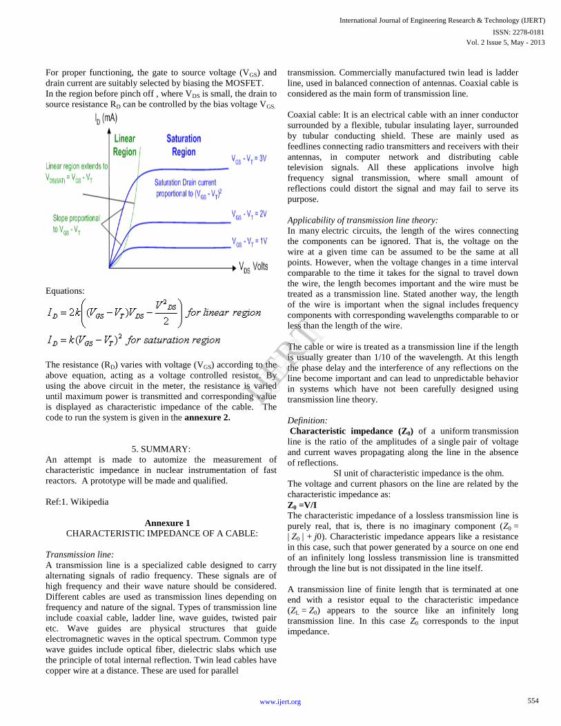
For proper functioning, the gate to source voltage (VGS) and
drain current are suitably selected by biasing the MOSFET.
In the region before pinch off , where VDS is small, the drain to
source resistance RD can be controlled by the bias voltage VGS.
Equations:
The resistance (RD) varies with voltage (VGS) according to the
above equation, acting as a voltage controlled resistor. By
using the above circuit in the meter, the resistance is varied
until maximum power is transmitted and corresponding value
is displayed as characteristic impedance of the cable. The
code to run the system is given in the annexure 2.
5. SUMMARY:
An attempt is made to automize the measurement of
characteristic impedance in nuclear instrumentation of fast
reactors. A prototype will be made and qualified.
Ref:1. Wikipedia
Annexure 1
CHARACTERISTIC IMPEDANCE OF A CABLE:
Transmission line:
A transmission line is a specialized cable designed to carry
alternating signals of radio frequency. These signals are of
high frequency and their wave nature should be considered.
Different cables are used as transmission lines depending on
frequency and nature of the signal. Types of transmission line
include coaxial cable, ladder line, wave guides, twisted pair
etc. Wave guides are physical structures that guide
electromagnetic waves in the optical spectrum. Common type
wave guides include optical fiber, dielectric slabs which use
the principle of total internal reflection. Twin lead cables have
copper wire at a distance. These are used for parallel
transmission. Commercially manufactured twin lead is ladder
line, used in balanced connection of antennas. Coaxial cable is
considered as the main form of transmission line.
Coaxial cable: It is an electrical cable with an inner conductor
surrounded by a flexible, tubular insulating layer, surrounded
by tubular conducting shield. These are mainly used as
feedlines connecting radio transmitters and receivers with their
antennas, in computer network and distributing cable
television signals. All these applications involve high
frequency signal transmission, where small amount of
reflections could distort the signal and may fail to serve its
purpose.
Applicability of transmission line theory:
In many electric circuits, the length of the wires connecting
the components can be ignored. That is, the voltage on the
wire at a given time can be assumed to be the same at all
points. However, when the voltage changes in a time interval
comparable to the time it takes for the signal to travel down
the wire, the length becomes important and the wire must be
treated as a transmission line. Stated another way, the length
of the wire is important when the signal includes frequency
components with corresponding wavelengths comparable to or
less than the length of the wire.
The cable or wire is treated as a transmission line if the length
is usually greater than 1/10 of the wavelength. At this length
the phase delay and the interference of any reflections on the
line become important and can lead to unpredictable behavior
in systems which have not been carefully designed using
transmission line theory.
Definition:
Characteristic impedance (Z0) of a uniform transmission
line is the ratio of the amplitudes of a single pair of voltage
and current waves propagating along the line in the absence
of reflections.
SI unit of characteristic impedance is the ohm.
The voltage and current phasors on the line are related by the
characteristic impedance as:
Z0 =V/I The characteristic impedance of a lossless transmission line is
purely real, that is, there is no imaginary component (Z0 =
| Z0 | + j0). Characteristic impedance appears like a resistance
in this case, such that power generated by a source on one end
of an infinitely long lossless transmission line is transmitted
through the line but is not dissipated in the line itself.
A transmission line of finite length that is terminated at one
end with a resistor equal to the characteristic impedance
(ZL = Z0) appears to the source like an infinitely long
transmission line. In this case Z0 corresponds to the input
impedance.
554
International Journal of Engineering Research & Technology (IJERT)
Vol. 2 Issue 5, May - 2013ISSN: 2278-0181
www.ijert.org
IJERT
IJERT
ZL = Z0
2.3.1 Transmission line model:
Every transmission line consists of circuit elements
distributed along its length. Because current flows through the
conductors, the line has series inductance, and because there is
always a return path, which is normally another adjacent
conductor, it has parallel capacitance. The series inductance
and parallel capacitance are the dominant elements in the
equivalent circuit of lines, and are present even in theoretically
perfect cases. But in real lines the conductors are not perfect,
so they also have some series resistance, and the dielectric or
insulation separating the two conductors is not perfect so it has
some parallel resistance. The series and parallel resistance are
less significant than the inductance and capacitance, unless
there is a fault in the line.
The transmission line model represents the transmission line
as an infinite series of two-port elementary components, each
representing an infinitesimally short segment of the
transmission line:
a) The distributed resistance R of the conductors is
represented by a series resistor (expressed in ohms
per unit length).
b) The distributed inductance L (due to the magnetic
field around the wires, self-inductance, etc.) is
represented by a series inductor (Henries per unit
length).
c) The capacitance C between the two conductors is
represented by a shunt capacitor C (farads per unit
length).
d) The conductance G of the dielectric material
separating the two conductors is represented by a
shunt resistor between the signal wire and the return
wire (Siemens per unit length).
In the real line the elements are distributed continuously along
the line, and are not lumped at intervals along the length as
shown.
In the above figure, each section of the equivalent circuit looks
like a low pass filter, so the effect of the inductance and
capacitance is to limit the bandwidth of the signals which the
line can transport, with higher frequencies being attenuated
more than lower ones. The series and parallel resistances
result in losses down the line, reducing the ability of the line to
transport the signal power efficiently
The characteristic impedance is given by
Z0
Where R, L, G, C are the corresponding values per unit length
and ω is angular frequency.
FOUR TERMINAL MODEL:
For the purposes of analysis, transmission line can be modeled
as a two-port network (also called a quadrupled network), as
follows:
In the simplest case, the network is assumed to be linear (i.e.
the complex voltage across either port is proportional to the
complex current flowing into it when there are no reflections),
and the two ports are assumed to be interchangeable. If the
transmission line is uniform along its length, then its
behaviour is largely described by the single parameter
characteristic impedance. Typical values of Z0 are 50 or
75 ohms for a coaxial cable, about 100 ohms for a twisted pair
of wires, and about 300 ohms for a common type of untwisted
pair used in radio transmission.
When sending power down a transmission line, it is usually
desirable that as much power as possible will be absorbed by
the load and as little as possible will be reflected back to the
source. This can be ensured by making the load impedance
equal to Z0, in which case the transmission line is said to
be matched.
INFINITE LENGTH CABLE:
Definition - The characteristic impedance, Z0, of a line is the
input impedance of an infinite length of the line.
The transmission line model of a cable can be simplified to an
equivalent circuit by using boxes to represent each section, as
shown below. The input impedance looking into the one end
of this infinite line can be taken as characteristic impedance
since the reflections are zero.
As the line is infinitely long, more sections can be added as
shown below, without making any difference to its properties.
555
International Journal of Engineering Research & Technology (IJERT)
Vol. 2 Issue 5, May - 2013ISSN: 2278-0181
www.ijert.org
IJERT
IJERT
Since the length is still infinite, the input impedance is still the
characteristic impedance.
The original line could be replaced by single impedance, Z0,
as shown below, and the input impedance would be
unchanged.
Therefore, if a finite length of line is terminated in its
characteristic impedance, Z0, then its input impedance will
also equal Z0 and it acts as infinite length line without any
reflections.
Annexure 2:
PROGRAM CODE:
void DAC_Init() //
to connect to dac
TRISD=0; //to declare portD as output
port
TRISC3_bit=0;
TRISC4_bit=0;
TRISC5_bit=0;
TRISC6_bit=0; //four more output pins
required for dac(12 bit)
TRISB4_bit=0; //to WR pin of
dac(declared as outputpin)
TRISB5_bit=0; //to CLR pin of
dac(declared as output)
TRISB6_bit=0; //to latch the dac(declared
as output)
PORTD=0; //to give a value of zero
initially(lower 8 bits)
PORTC=0; //to give a value of zero
initially(upper 4 bits)
RB4_bit=1; //set WR pin
RB5_bit=1; // clear this bit to clear the
dac
RB6_bit=1; //clear this bit to latch the
value
void memory_check()
char temp=0,temp1=0; // variables declared to assign
values and to retrieve values
FSR0=0;
do
INDF0=FSR0;//assign the address value to the
register
temp= INDF0; //retrieve the value from the
memory
if(temp!=FSR0) //compare the value to check
Lcd_Init(); //to initialise lcd (connect the pins)
Lcd_Out_Cp(" memory incorrect"); //display the
memory is not working using built in lcd function
break; //**command to halt the uc or go to
off mode
Else
FSR0++;
while(FSR0<=0xFF);
temp=0;
for(FSR0=0xFF;FSR0<=0xFFF;FSR0++,temp++)//
after FSR0=0xFF, FSR0 cannot be assigned to the
memory register
INDF0=temp;
temp1=INDF0;
if(temp1!=temp)
Lcd_Init(); //to initialise lcd
Lcd_Out_Cp(" memory incorrect"); //display the
memory is not working
break; //**command to halt the uc or go to
off mode
for(FSR0=0x00;FSR0<=0x3FF;FSR0++)
INDF0=0;//to initiate all the memory locations to
zero
void dac_adc_check()
ADC_init();
DAC_init();
RA2_bit=1;
PORTD=0x088;
if(ADRES!=0x88)
Lcd_Init();
Lcd_Out_Cp(" adc or dac not working");
//**command to exit from the program
int voltage;
int voltage_from_lookup_table(int resistance)
//luk up using table in memory
TBLPTR= 0x266+resistance; // say 0x266 has
voltage value for zero resistance, where the table
starts
//**command to read frm memory TBLRD*;
//**read into TABLAT and increment
voltage= TABLAT ; //get data
556
International Journal of Engineering Research & Technology (IJERT)
Vol. 2 Issue 5, May - 2013ISSN: 2278-0181
www.ijert.org
IJERT
IJERT
return voltage;
int resistance_for_known_voltage(int voltage)
// function to get resistance for voltage transmitted,
for Zoc and Zsc
int *ptr;
int temp=0;
int resistance;
do
temp++;
ptr=0x266+temp;
while(voltage<=(*ptr)&& temp<=1000);
if(temp>=1000) //to check if Z is
in the range of 10ohm to 1000ohm
Lcd_Out_Cp(" ci is not in range"); //to
declare Zoc or Zsc are not in the range
//**command to exit //** to halt the program
at this point
resistance=*ptr;
return resistance; // return the value to assign it to
Zoc or Zsc
ADC_Init(); // Initialize ADC
module with default settings
unsigned ADC_Get_Sample(unsigned short channel);
//default function of adc to get analog value from the
specified channel
unsigned ADC_Read(unsigned short channel);
//default functions in the library to get the digital
value into a variable
int adc_output_peak_voltage() //to get the
peak voltage value to be used in power calculation
int output_adc[30];
int vnum=1;
int temp;
output_adc[0]=0;
do
output_adc[vnum]=ADC_Get_Sample(7);
temp=vnum-1;
if(output_adc[vnum]<output_adc[temp])
output_adc[vnum]=output_adc[temp];
while(vnum<=30);
return output_adc[30];
void latch_init()
RE0_bit=0; //to enable output of
the latch
RE1_bit= 1; //to select the latch
int voltage_frm_lukup_table(int resistance) // luk up
using pointers
int *ptr; //declare a pointer
ptr=0x266+resistance; //get the adress of the voltage
required at ptr assuming tabular values start at 0x266
voltage=*ptr; //store the value at voltage variable
return voltage;
void dac_output_voltage(int resis)()
int voltag;
voltag= voltage_frm_lukup_table(resis);
PORTD=voltag;
RC3_bit=voltag>>8;
RC4_bit=voltag>>9;
RC5_bit=voltag>>10;
RC6_bit=voltag>>11;
//pins assigned to control switches
// Lcd pinout settings
sbit LCD_RS at RA4_bit;
sbit LCD_EN at RA3_bit;
sbit LCD_D7 at RD7_bit;
sbit LCD_D6 at RD6_bit;
sbit LCD_D5 at RD5_bit;
sbit LCD_D4 at RD4_bit;
sbit LCD_D3 at RD3_bit;
sbit LCD_D2 at RD2_bit;
sbit LCD_D1 at RD1_bit;
sbit LCD_D0 at RD0_bit;
sbit LCD_RS_Direction at TRISA4_bit;
sbit LCD_EN_Direction at TRISA3_bit;
sbit LCD_D7_Direction at TRISD7_bit;
sbit LCD_D6_Direction at TRISD6_bit;
sbit LCD_D5_Direction at TRISD5_bit;
sbit LCD_D4_Direction at TRISD4_bit;
sbit LCD_D3_Direction at TRISD3_bit;
sbit LCD_D2_Direction at TRISD2_bit;
sbit LCD_D1_Direction at TRISD1_bit;
sbit LCD_D0_Direction at TRISD0_bit;
int Zi;
int Z0;
int v;
int temp1,temp2;
unsigned int vcr,m;
double power[100];
void main()
Lcd_Init();
Lcd_Out_Cp("connect the cable"); //
start of the program
RE0_bit=0; //to latch the lcd
DAC_Init();
Zi=10;
do
dac_output_voltage(Zi);
v =adc_output_peak_voltage() ;
power[m]=(v*v)/Zi;
Zi++;
while((power[Zi-2]>power[Zi-1])|| (power[Zi-
1]>power[Zi-3]));
RB6_bit=0; //to latch dac
Z0=Zi-3+10; //Zi-3+10 is the value of the
impedance where maximum power transmissin
occurs, +10 for series resistance
Lcd_Init();
557
International Journal of Engineering Research & Technology (IJERT)
Vol. 2 Issue 5, May - 2013ISSN: 2278-0181
www.ijert.org
IJERT
IJERT

Lcd_Out(1,1,&Zi); // display characteristic
impedance
void test_mode()
RA0_bit=1;
Lcd_Init();
Lcd_Out_Cp("test mode"); // start of the
program
RE0_bit=0; //to latch the lcd
DAC_Init();
Zi=10;
do
dac_output_voltage(Zi);
v =adc_output_peak_voltage() ;
power[m]=(v*v)/Zi;
Zi++;
while((power[Zi-2]>power[Zi-1])|| (power[Zi-
1]>power[Zi-3]));
RB6_bit=0; //to latch dac
Z0=Zi-3+10; //Zi-3+10 is the value of the
impedance where maximum power transmissin
occurs, +10 for series resistance
Lcd_Init();
if(Z0==75)
Lcd_Out_Cp("working normal, no error");
Else
Lcd_Out_Cp("error, test result not equal to 75");
void reset_mode()
Lcd_Cmd(_LCD_CLEAR); // Clear Lcd
display
main();
*
558
International Journal of Engineering Research & Technology (IJERT)
Vol. 2 Issue 5, May - 2013ISSN: 2278-0181
www.ijert.org
IJERT
IJERT


![On the Superposition and Elastic Recoil of Electromagnetic ... · the deviation of wave impedance from characteristic impedance in the presence of a reflected wave [6] and others](https://img.pdfslide.net/doc/110x75/6007b6d7cdf07a5e05396b64/on-the-superposition-and-elastic-recoil-of-electromagnetic-the-deviation-of.jpg)