Embed Size (px)
Citation preview

HAL Id tel-01512657httpstelarchives-ouvertesfrtel-01512657
Submitted on 24 Apr 2017
HAL is a multi-disciplinary open accessarchive for the deposit and dissemination of sci-entific research documents whether they are pub-lished or not The documents may come fromteaching and research institutions in France orabroad or from public or private research centers
Lrsquoarchive ouverte pluridisciplinaire HAL estdestineacutee au deacutepocirct et agrave la diffusion de documentsscientifiques de niveau recherche publieacutes ou noneacutemanant des eacutetablissements drsquoenseignement et derecherche franccedilais ou eacutetrangers des laboratoirespublics ou priveacutes
Development of charged particle detection systems formaterials analysis with rapid ion beams large solid
angle detectors and numerical nuclear pulse processingViacutector Alarcoacuten Diacuteez
To cite this versionViacutector Alarcoacuten Diacuteez Development of charged particle detection systems for materials analysis withrapid ion beams large solid angle detectors and numerical nuclear pulse processing Physics [physics]Universiteacute Pierre et Marie Curie - Paris VI 2016 English NNT 2016PA066489 tel-01512657
Universiteacute Pierre et Marie Curie Ecole doctorale Physique et Chimie des Mateacuteriaux ndash ED 397
Institute de NanoScience de Paris - UMR7586
Couches nanomeacutetriques formation interfaces et deacutefauts
Development of Charged Particle Detection Systems for Materials Analysis With Rapid Ion Beams
Large solid angle detectors and numerical nuclear pulse processing
Par Viacutector Alarcoacuten Diacuteez
Thegravese de doctorat de Physique
Dirigeacutee par Ian C Vickridge
Preacutesenteacutee et soutenue publiquement le 14-12-2016
Devant un jury composeacute de
Dr DOEBELI Max Chercheur ETH Zurich Rapporteur
Dr ZUCCHIATTI Alessandro Professeur UAM Rapporteur
Dr ALQUIE Georges Professeur emerite UPMC Examinateur
Dr KHODJA Hicham Chercheur CEA Examinateur
Dr MONCOFFRE Nathalie Chercheur CNRS Examinatrice
Dr VICKRIDGE Ian Chercheur CNRS Directeur de thegravese
Development of Charged Particle Detection Systems for Materials Analysis With Rapid Ion Beams1
Large solid angle detectors and numerical nuclear pulse processing
Deacuteveloppent de systegraveme de deacutetection de particules pour analyse de mateacuteriaux avec faisceau drsquoions
Deacutetecteur de grande angle solide et traitement numeacuterique des impulsions nucleacuteaires
Par Viacutector Alarcoacuten Diacuteez
1 This thesis has been supported by Marie Curie Actions ndash Initial Training Networks (ITN) within the project Supporting Postgraduate Research with Internships in Industry and Training Excellence (SPRITE) under EC contract No 317169
ldquoEl mundo es como aparece ante mis cinco sentidos y ante los tuyos que son las
orillas de los miacuteosrdquo
― Miguel Hernaacutendez ―
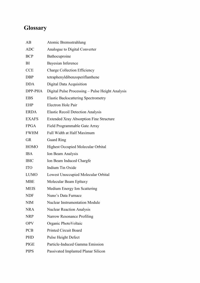
Glossary
AB Atomic Bremsstrahlung
ADC Analogue to Digital Converter
BCP Bathocuproine
BI Bayesian Inference
CCE Charge Collection Efficiency
DBP tetraphenyldibenzoperiflanthene
DDA Digital Data Acquisition
DPP-PHA Digital Pulse Processing ndash Pulse Height Analysis
EBS Elastic Backscattering Spectrometry
EHP Electron Hole Pair
ERDA Elastic Recoil Detection Analysis
EXAFS Extended Xray Absorption Fine Structure
FPGA Field Programmable Gate Array
FWHM Full Width at Half Maximum
GR Guard Ring
HOMO Highest Occupied Molecular Orbital
IBA Ion Beam Analysis
IBIC Ion Beam Induced Chargfe
ITO Indium Tin Oxide
LUMO Lowest Unoccupied Molecular Orbital
MBE Molecular Beam Epicirctaxy
MEIS Medium Energy Ion Scattering
NDF Nunorsquos Data Furnace
NIM Nuclear Instrumentation Module
NRA Nuclear Reaction Analysis
NRP Narrow Resonance Profiling
OPV Organic PhotoVoltaic
PCB Printed Circuit Board
PHD Pulse Height Defect
PIGE Particle-Induced Gamma Emission
PIPS Passivated Implanted Planar Silicon
PIXE Particle-Induced X-ray Emission
QFEB Quasi Free Electron Bremsstrahlung
QL Quintuple Layer
QSH Quantum Spin Hall effect
RBS Rutherford Backscattering Spectrometry
SAFIR Systegraveme drsquoAnalyse par Faisceaux drsquoIons Rapides
SEB Secondary Electron Brehmsstrahlung
SegDet Segmented Detector
SIMS Secondary Ion Mass Spectrometry
SA Simulated Annealing
TFU Thin Film Unit (1015 cm-2)
TI Topological Insulator
TMO Transition Metal Oxide
TR Time Reversal
TSS Topological Surface State
WF Work Function
XRF X-ray Fluorescence
1
Contents
Abstract 3
Reacutesumeacute 4
Resumen 16
Acknowledgements 17
1 Introduction 19
11 Ion beam Analysis (IBA) Techniques 20
111 Rutherford Backscattering Spectroscopy (RBS) 22
112 Channelling 28
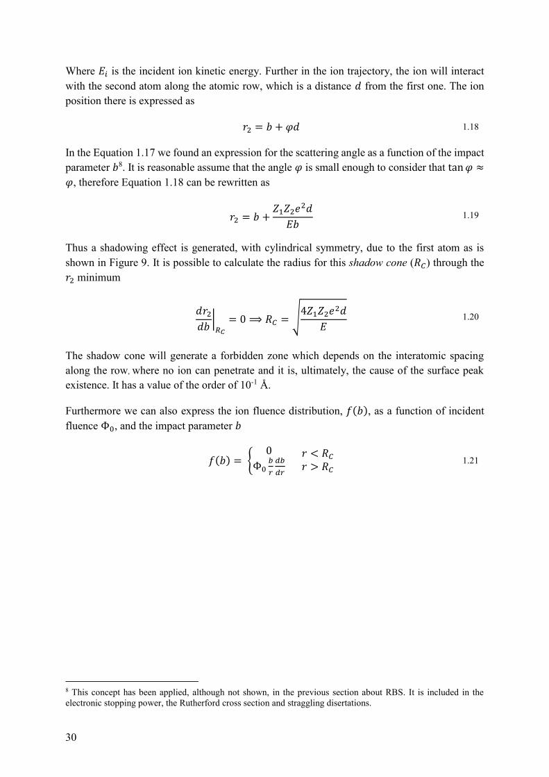
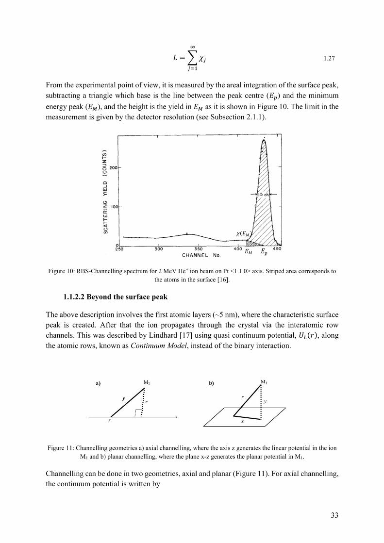
1121 Surface peak 29
1122 Beyond the surface peak 33
113 Particle Induce X-ray Emission (PIXE) 37
114 Nuclear Reaction Analysis (NRA) 39
115 Ion Beam Induction Charge (IBIC) 41
12 Topological Insulators (TI) 43
13 Organic Semiconductor Devices 46
2 Charged Particle Detection 48
21 Semiconductor Detectors 48
211 Single Detector 49
212 Segmented Detector 52
2121 Charge Collection Efficiency Publication I 55
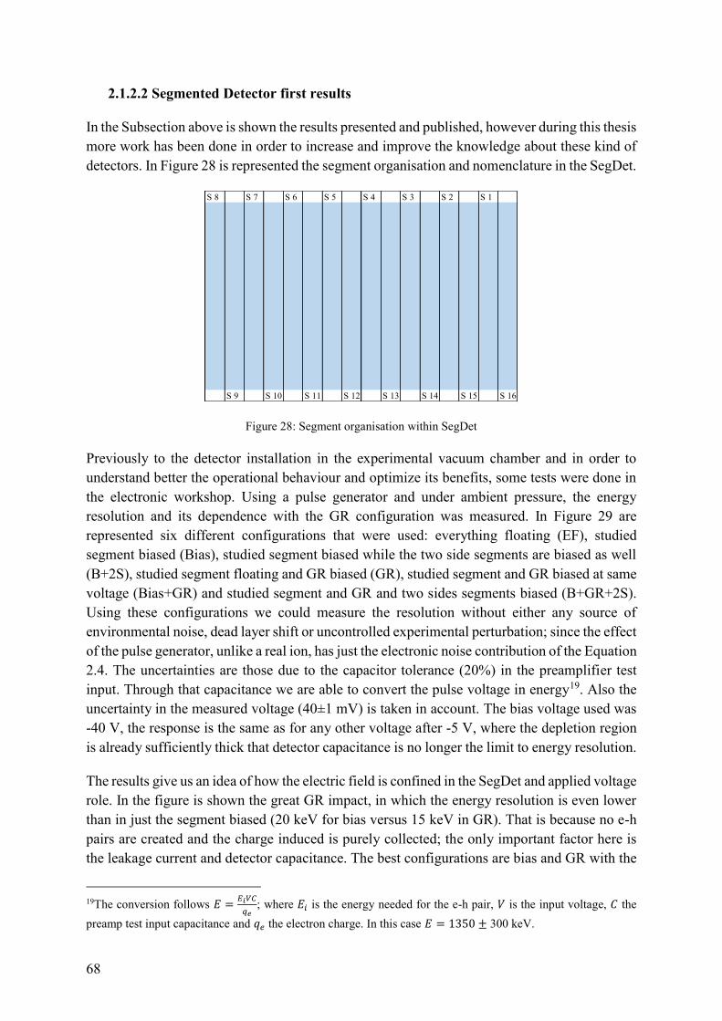
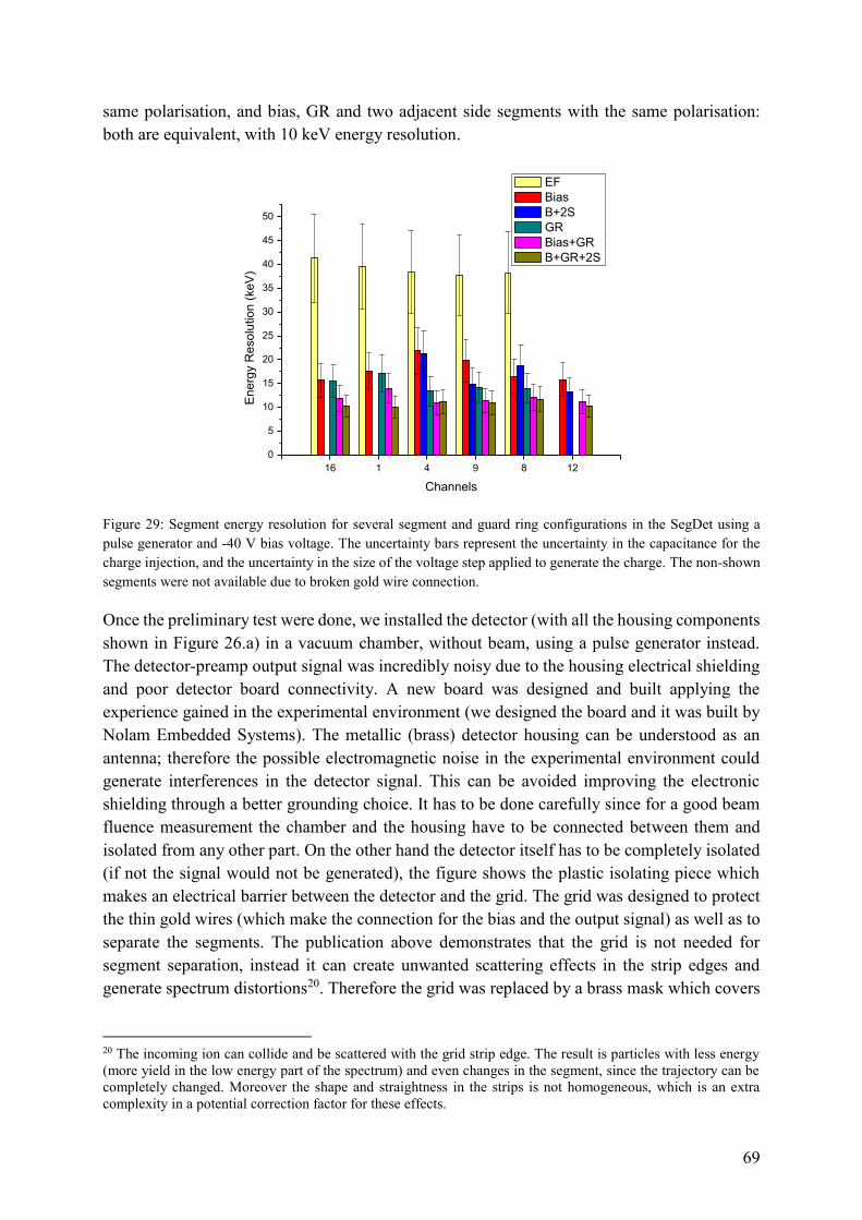
2122 Segmented Detector first results 68
213 Annular Detector 72
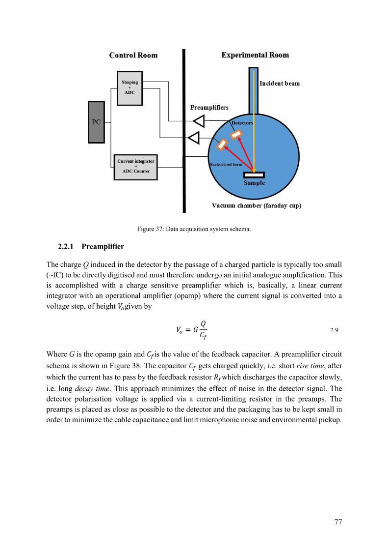
22 Signal Acquisition and Treatment 76
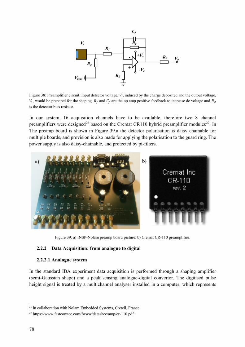
221 Preamplifier 77
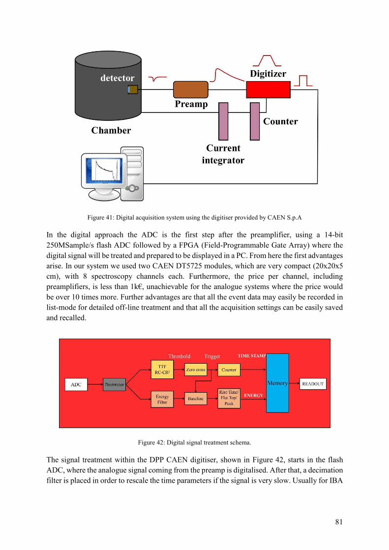
222 Data Acquisition from analogue to digital 78
2221 Analogue system 78
2222 Digital system 80
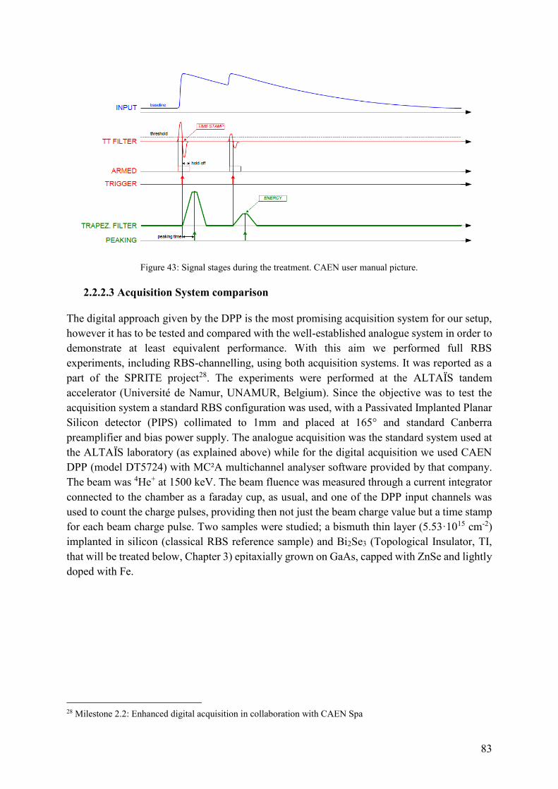
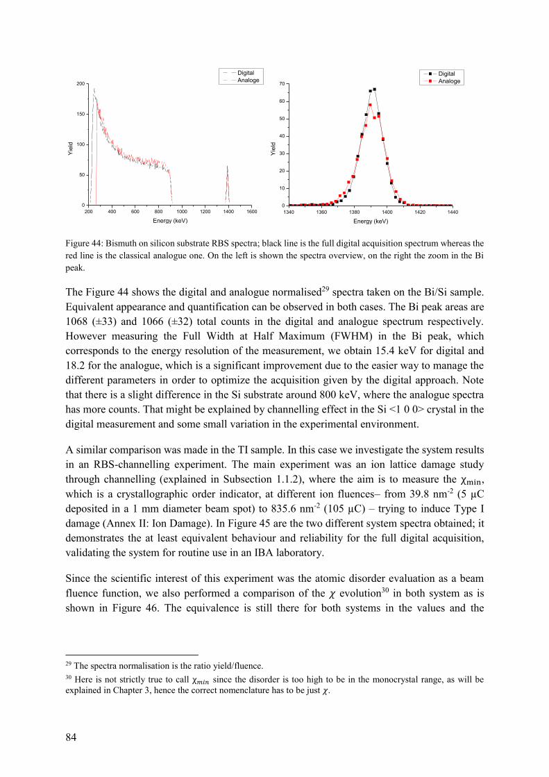
2223 Acquisition System comparison 83
3 IBA in Topological Insulators 86
31 Motivation 86
2
32 Samples and Experimental Setup 87
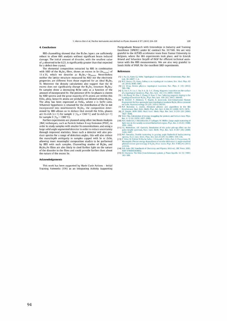
33 Results Publication II 89
34 Results Non-published 95
341 Composition quantification NDF Fitting 95
342 Channelling 98
343 Segmented Detector in TI 101
3431 Channelling with SegDet 103
35 Conclusions and perspectives concerning TI 104
4 MoOx and Organic Semiconductors Devices 107
41 Motivation 107
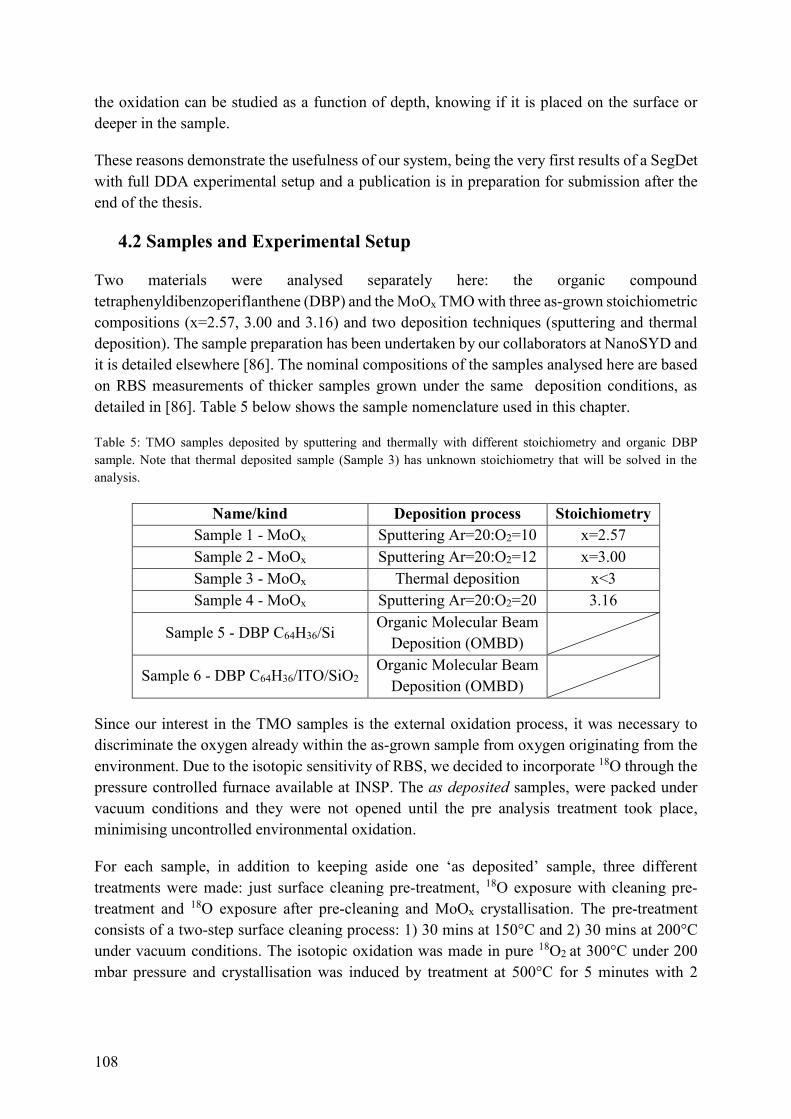
42 Samples and Experimental Setup 108
43 Results and Discussion 110
431 MoOx oxidation stoichiometry and external oxygen characterisation 110
432 Organic semiconductor overcoming classical RBS limitations 116
44 Conclusions of the MoOxDBP study 119
5 Conclusions and Perspectives 122
Annex I NDF DataFurnace and Total IBA 125
Annex II Ion Damage 128
Bibliography 131
Figures 139
Tables 144
3
Abstract
This thesis presents the technical improvements made in IBA (Ion Beam Analysis) for the SAFIR platform (UPMC-INSP Paris France) and a selection of associated scientific applications The main improvements are the increased solid angle in a custom silicon-based semiconductor segmented detector and the associated data acquisition system These improvements open the way to substantially improved spectrum statistics for a given analysing beam fluence and the possibility to perform realistic analyses with very low beam fluences for example on very sensitive samples or with beams of very low intensity
IBA has been used for materials characterisation since the 1970rsquos mainly focused on semiconductor technology which is the base for the electronic technology used nowadays In the beginning of the XXI century new technological challenges (lower power consumption more storage higher speedhellip) are imposed and new materials beyond classical semiconductors are emerging (spin tuneable materials topological insulators organic semiconductorshellip) IBA needs to evolve to meet the challenges in analysing some of these new materials since detection and data acquisition systems have not been really updated for years
The large solid angle Segmented Detector (SegDet) overcomes some of the limitations related to the charged particle detection system IBA techniques exploit the different ion-matter interactions (Rutherford nuclear reaction x-rays productionhellip) and the statistical nature of these interactions means that the statistics of the detected particles is a critical parameter A larger detector solid angle ndash eg for RBS Rutherford Backscattering Spectrometry more than 50 times that of a standard detector ndash represents a great improvement The large detector area has to be segmented in order to maintain good energy resolution Our device was divided into 16 side-to-side segments separated by a voltage guard ring This requires 16 independent particle spectroscopy channels which is complicated and expensive to implement using the classical analogue systems We have demonstrated the possibility to use a low cost and highly reproducible Digital Data Acquisition (DDA) system through numerical nuclear pulse processing for each individual segment and shown performance at least equivalent to that of an analogue system The SegDet was completely characterised in terms of depletion thickness leakage current charge collection efficiency and energy resolution
Very ionisation sensitive materials such as the organic compounds were not possible to study since the ion beam modify or destroy the samples before the statistics were satisfying to be interpreted using the SegDet are now available to analyse Furthermore the samples with small amount of matter such as ferromagnetic doped materials for spintronic or oxidation processes can be analysed within a reasonable beam fluence giving good statistical results In this thesis we demonstrate both applications getting valuable results for iron-contain Bi2Se3 topological insulator transition metal oxide MoOx oxidation process and organic semiconductor tetraphenyldibenzoperiflanthene (DBP) elemental analysis Moreover the statistical improvement has been used to extend the maximum capabilities for a single ended 2 MV Van de Graaff accelerator by using the doubly charged ions such as 4He2+ produced at very low fluences by the RF ion source to perform RBS at energies up to 4 MeV
4
Reacutesumeacute
Cette thegravese preacutesente un travail visant agrave lrsquoameacutelioration des techniques drsquoIBA (Ion Beam Analysis ndash Analyse par Faisceau drsquoIons) pour la plateforme SAFIR de lrsquoINSP (Institute de NanoScicence de Paris UPMC) baseacutee sur un deacutetecteur segmenteacute de grand angle solide avec un systegraveme tout numeacuterique de traitement de signaux associeacute Les possibiliteacutes drsquoanalyse du systegraveme ainsi mis en œuvre sont deacutemontreacutees agrave travers quelques applications dans le domaine de la physique et la science de mateacuteriaux Lrsquoaugmentation de lrsquoangle solide de deacutetection est le principal avantage permettant une diminution consideacuterable de lrsquoincertitude lieacutee agrave la statistique de comptage pour une fluence donneacutee drsquoions incidents Ce deacuteveloppement ouvre la voie agrave des eacutetudes de tregraves faibles quantiteacutes de matiegravere ou des pics de faible intensiteacute sur un fond important agrave lrsquoeacutetude de mateacuteriaux sensibles aux deacutegacircts induits par le faisceau incident ou encore agrave lrsquoexploitation de faisceaux de tregraves faible intensiteacute
La thegravese est diviseacutee en trois grandes parties une premiegravere partie theacuteorique qui preacutesente les concepts physiques sous-entendant les diffeacuterentes techniques IBA une deuxiegraveme partie plus technique deacutetaillant les deacuteveloppement et la mise en œuvre du systegraveme de deacutetection ainsi que le traitement lsquoself-consistentrsquo de la grande quantiteacute drsquoinformation recuillie avec ce nouveaux systegraveme et une troisiegraveme partie preacutesentant les premiers reacutesultats obtenus en sciences des mateacuteriaux en appliquant le systegraveme ainsi mis en œuvre
Introduction aux techniques IBA
LrsquoIBA est une meacutethode de caracteacuterisation des mateacuteriaux deacuteveloppeacutee depuis les anneacutees 1970 geacuteneacuteralement pour lrsquoeacutetude des semi-conducteurs mais eacutegalement avec applications en geacuteologie sciences du patrimoine et meacutedecine entres autres Dans tous les cas les ions geacutenegravereacutes agrave partir drsquoun gaz ioniseacute ou par pulveacuterisation sont acceacutelegravereacutes aux eacutenergies entre 01 et 10 MeV et sont dirigeacutes sous vide avec des champs magneacutetiques ou eacutelectriques sur lrsquoeacutechantillon objet de lrsquoanayse normalement situeacute lui aussi dans une chambre sous vide Les ions peuvent donner lieu agrave plusieurs types drsquointeractions avec les atomes lrsquoeacutechantillon et crsquoest en mesurant le nombre des produits de ces interactions ainsi que leurs spectres en eacutenergie que lrsquoanalyse de la composition et dans certains cas de la structure cristalline de lrsquoechantillon srsquoeffectue La mesure des ions retrodiffuseacutes eacutelastiquement est agrave la base de la meacutethode RBS (Rutherford Backscattering Spectrometry) La mesure des rayons X caracteacuteristiques induit par les ions incidents est agrave la base de la meacutethode PIXE (Particle Induced Xray Emission) Enfin la mesure des produits de reacuteactions nucleacuteaires est agrave la base des meacutethodes PIGE (Particle Induced Gamma Emission) NRA (Nuclear Reaction Analysis) et dans le cas speacutecifique ougrave une section efficace drsquoune reacuteaction nucleacuteaire preacutesente des reacutesonances eacutetroites agrave la meacutethode NRP (Narrow Resonance Profiling)
Toutefois la teacutechnologie derriegravere ces meacutethodes drsquoanalyse est neacutee au deacutebut de la deuxiegraveme moitieacute du XXegraveme seigle quand le principal sujet drsquoeacutetude eacutetait la physique nucleacuteaire via les reacuteactions nucleacuteaires etudieacutees avec des acceacuteleacuterateurs eacutelectrostatiques drsquoions de tension de lrsquoordre du meacutega-Volt Les besoins drsquoeacutetudes en physique nucleacuteaire vers les plus hautes eacutenergies
5
et lrsquoeacutetat de connaissance de cette discipline aux basses eacutenergies ont permi de reconvertir les laquo petitsraquo acceacuteleacuterateurs agrave des fins drsquoanalyses de la matiegravere condenseacutee Il srsquoagira cette fois drsquoidentifier une atome de une cible2 agrave partir drsquoune particule inciedente connue De plus il eacutetait tentant de ne pas abandonner ces petits acceacuteleacuterateurs qui avaient fait lrsquoobjet drsquoinvestissements importants Ainsi les techniques IBA sont neacutees et sont maintenant largement utiliseacutees pour lrsquoanalyse de la composition et de la structure de la reacutegion superficielle des mateacuteriaux Dans les anneacutees 1960 lrsquoacceacuteleacuterateur de SAFIR eacutetait le premier au monde agrave ecirctre conccedilu speacutecifiquement pour lrsquoIBA et ecirctre installeacute non plus dans un centre de recherches nucleacuteaires mais dans un laboratoire de physique des solides
Dans cette thegravese trois techniques majeures de lrsquoIBA sont exploiteacutees RBS PIXE et NRA Apregraves une preacutesentation de la perte drsquoeacutenergie continue des particules dans la matiegravere qui est un processus commun agrave toutes les techniques IBA ces trois techniques sont preacutesenteacutees plus en deacutetails dans la section qui suit La technique drsquoIon beam Induced Charge (IBIC) est preacutesenteacute dans la section du reacutesumeacute deacutedieacutee agrave la caracteacuterisation du deacutetecteur segmenteacute tandis qursquoune preacutesentation deacutetailleacutee de la canalisation des particules dans un monocristal deacutepasse le cadre de ce reacutesumeacute Le lecteur est reacutefereacute agrave la section 112 de la thegravese pour plus de deacutetails
Pouvoir drsquoarrecirct
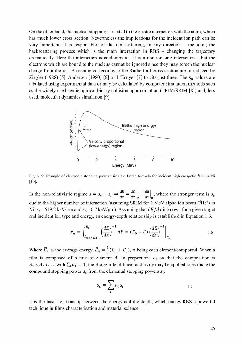
Lrsquointeraction la plus probable entre un ion et la matiegravere qursquoil traverse est la perte drsquoeacutenergie eacutelectronique et cette interaction est importante pour toutes les meacutethodes IBA En effet lrsquoion incident subit un grand nombre de chocs avec les eacutelectrons ndash quelques chocs pour chaque nm traverseacute en perdant une faible quantiteacute drsquoeacutenergie dans chaque choc On distingue donc pour des interactions avec une atome de la cible des chocs eacutelastiques (lrsquoeacutenergie cinetique est conserveacutee) et des chocs ineacutelastiques (une partie de lrsquoeacutenergie cineacutetique de la collision est absorbeacutee pour arracher lrsquoeacutelectron de son site) Agrave une eacutechelle macroscopique cette perte drsquoeacutenergie eacutelectronique peut ecirctre considreacutee comme eacutetant continue La perte moyenne par uniteacute de longueur fonction du mateacuteriau et de la vitesse de lrsquoion est donc deacutefinie de maniegravere diffeacuterentielle en le nomant le pouvoir drsquoarrecirct 119904 = 119889119864119889119909 Un proton de 1 MeV travsersant le silicium perd 41 eV par nm traverseacute A cette perte devrait srsquoajouter eacutegalement la perte drsquoeacutenergie ducirce aux interactions faibles avec les noyaux atomiques ndash eacutegalement constitueacutee drsquoune seacuterie drsquointeractions avec une faible perte dans chaque interaction Ces pertes nucleacuteaires sont neacutegligeables devant les pertes eacutelectroniques Le pouvoir drsquoarrecirct est donc donneacute par 119904 = 119904119899 + 119904119890 ougrave 119904119899 ≪ 119904119890 dans le domaine de lrsquoIBA
2 Si pour les physiciens nucleacuteaires il srsquoagit drsquoenvoyer des ions sur une cible pour lrsquoanalyste il srsquoagit drsquoenvoyer des ions sur un eacutechantillon Du fait de lrsquoheacuteritage lsquonucleacuteairersquo de lrsquoIBA on parle encore parfois drsquoune cible mecircme pour lrsquoanalyse
6
RBS ndash Rutherford Backscattering Spectrometry ndash Spectromeacutetrie de la Reacutetrodiffusion
de Rutherford
La RBS est sans doute la technique la plus utiliseacutee dans le domaine drsquoIBA Ici on profite de lrsquointeraction eacutelastique entre les ions leacutegers (chargeacutes positivement) et les noyaux atomiques de la cible ougrave la section efficace de reacutetrodiffusion est Rutherford - analytique et bien connue Si la fluence du faisceau incident (nombre drsquoions par uniteacute de surface) est connue on peut remonter quantitativement agrave la composition de la cible
En RBS on peut consideacuterer que lrsquoion incident subit une interaction purement Coulombienne (et donc ayant la section efficace de Rutherford) avec un noyau atomique La quantiteacute de mouvement et lrsquoeacutenergie cineacutetique sont conserveacutees ce qui permet de deacuteduire facilement la section efficace de lrsquointeraction ainsi que lrsquoeacutenergie de lrsquoion apregraves lrsquointeraction (et par conseacutequent aussi lrsquoeacutenergie ceacutedeacutee au noyau cible) ndash la cineacutematique de lrsquointeraction La section efficace de Rutherford est proportionnelle au carreacute du numeacutero atomique du noyau cible et est donc tregraves avantageuse pour des noyaux lourds mais limiteacutee pour des noyaux leacutegers En cas de reacutetrodiffusion (la trajectoire de lrsquoion est deacutevieacutee de plus de 90deg) plus le noyau est lourd plus lrsquoion incident garde son eacutenergie initiale Si le noyau eacutetait infiniment lourd lrsquoion ne ceacutedeacuterait aucune eacutenergie au noyau et conserverait donc son eacutenergie initiale Dans le cas contraire ougrave le noyau cible aurait la mecircme masse que lrsquoion incident la reacutetrodiffusion serait impossible ndash lrsquoion reviendrait avec lsquozeacuterorsquo eacutenergie Un spectre en eacutenergie des ions reacutetrodiffuseacutes est ainsi une sorte de spectromeacutetrie de masse des noyaux de la cible Notons ici que cette sensibiliteacute agrave la masse donne donc une sensibiliteacute aux diffeacuterents isotopes De plus les ions perdent leur eacutenergie via le processus quasi-continu du pouvoir drsquoarrecirct Un ion reacutetrodiffuseacute sur un noyau agrave la surface de la cible revient avec lrsquoeacutenergie donneacutee par la cineacutematique alors qursquoun ion reacutetrodiffuseacute par le mecircme noyau agrave une certaine profondeur dans la cible aura perdu de lrsquoeacutenergie sur les trajets aller et retour dans la cible et reviendra donc avec moins drsquoeacutenergie Le spectre en eacutenergie contient donc aussi des informations sur la profondeur agrave laquelle srsquoest trouveacute le noyau cible et ainsi constitue aussi une mesure de profil de concentration en profondeur Du fait que les interactions sont parfaitement connues la RBS est absolument quantitative
Toutefois la reacutesolution en masse et la reacutesolution en eacutenergie de la RBS sont limiteacutees par la reacutesolution en eacutenergie du deacutetecteur La sensibiliteacute est limiteacutee par la statistique de comptage pour un pic caracteacuteristique ndash soit isoleacute soit sur un fond provenant drsquoautres noyaux dans la cible Crsquoest dans ce dernier cas que la grand angle solide du deacutetecteur segmenteacute donne un avantage consdeacuterable par rapport aux deacutetecteurs de particules classiques
PIXE ndash Particle Induced X ray Emission ndash Emission de rayons X Induis par Particules
Avec une probabiliteacute beacoup plus petite que celle drsquoune interaction de perte drsquoeacutenergie eacuteleacutectronique lrsquoion peut ioniser une atome cible dans une couche eacutelectronique interne Un photon est eacutemis quand un eacutelectron drsquoune couche exteacuterieur tombe dans le trou laisseacute par lrsquoelectron eacutejecteacute et son eacutenergie est caracteacuteristique de lrsquoatome ioniseacute Agrave la diffeacuterence avec la RBS lrsquoenergie du rayon X est une signature atomique et pas isotopique Pour un eacuteleacutement donneacute
7
lrsquoionisation peut se faire dans une diverses couches et sous-couches internes et lrsquoeacutelectron qui va combler le trou peut provenir lui aussi drsquoune des diverse couches et sous-couches externes donnant lieu agrave des rayons X de diffeacuterentes eacutenergies et intensiteacutes Le processus eacutetant tregraves similaire agrave celui agrave la base de la fluorescence X le nomenclature des raies y est identique Notons ici que lrsquoeacutenergie des rayons X ne depend pas de la profondeur agrave laquelle ils ont eacuteteacute induits un spectre PIXE ne contient aucune information sur les profils de concentration des eacuteleacutements deacutetecteacutes
Le PIXE neacutecessite un deacutetecteur speacutecialiseacute typiquement un deacutetecteur agrave seacutemiconducteur drsquoune grande eacutepaisseur pour aborber les rayons X drsquoeacutenergie jusqursquoagrave 20 keV et refroidi afin drsquoobtenir une reacutesolution en eacutenergie suffisante
De par les sections efficaces drsquoionisation et drsquoemission des rayons X le PIXE est particuliegraverement bien adapteacute pour la deacuteterminations de concentrations drsquoeacuteleacutements de masse moyenne (Si jusqursquoagrave Ag) et peut ecirctre un compleacutement inteacuteressant agrave la RBS dans les cas ougrave la reacutesolution en masse de ce dernier est insuffisante ou alors ougrave dans les cas ougrave le signal drsquoun eacuteleacutement en RBS est noyeacute dans un grand fond
NRA ndash Nuclear Reaction Analysis ndash Analyse par Reacuteactions Nucleacuteaires
Les ions incident sur les noyaux de la cible peuvent induire des reacuteactions nucleacuteaires telle que 18O(p)15N Ici un proton incident sur un noyau 18O produit une particule alpha et laisse le noyau reacutesiduel 15N Dans une reacuteaction nulceacuteaire il y a reacuteorganisation de la structure interne des nouyaux impliqueacutes Il peut y avoir eacutechange de nucleacuteons excitation des eacutetats nucleacuteaires internes etou eacutemission de produits de reacuteactions ndash particules photons particules sub-nucleacuteaires La reacuteaction peut consommer (reacuteaction endothermique) ou relacher (reacuteaction exothermique) de lrsquoeacutenergie La reacuteaction nrsquoest plus eacutelastique car lrsquoeacutenergie cineacutetique nrsquoest pas conserveacutee seule la masse-eacutenergie est conserveacutee NRA est la technique IBA qui utilise les produits des reacuteactions nucleacuteaires exothermiques (et dont par conseacutequent les produits de reacuteaction sont assez eacutenergeacutetiques) pour deacuteterminer la quantiteacute de matiegravere dans une cible Ces reacuteactions typiquement ont une section efficace assez basse par rapport agrave la reacutetrodiffusion de Rutherford Les connaissances de la physique nucleacuteaire ne permettent pas encore de calculer leurs sections efficaces agrave priori De plus ces sections efficaces peuvent varier fortement avec la nature et lrsquoeacutenergie des ions incidents et en fonction de lrsquoangle de deacutetection Toutefois une fois la chaleur de reacuteaction connue la cineacutematique suit des lois de collisions classiques analogues agrave la RBS Notons ici que les reacuteactions nucleacuteaires sont speacutecifiques aux expegraveces nucleacuteaires et donc aux isotopes La NRA est par conseacutequent adapteacutee agrave la caracteacuterisation des isotopes La gamme drsquoeacuteleacutements deacutetectables avec la NRA est tregraves large mais crsquoest utiliseacute surtout pour les eacuteleacutements plus leacutegers ougrave drsquoautres techniques drsquoIBA ne sont pas adapteacutees
Du fait que les sections efficaces sont faibles de grandes fluences sont neacutecessaires afin drsquoobteacutenir des statistiques de comptage convenables et de grands currents de faisceau (plusieurs centaines de nA) sont utiliseacutes Ceci engendre un tregraves grand flux de particules diffuseacutees eacutelastiquement qui peuvent saturer le deacutetecteur et les chaines drsquoacquisition Les produits des
8
reacuteactions nucleacuteaires utiliseacutees en NRA sont suffisamment eacutenergeacutetiques qursquoil suffit de placer devant le deacutetecteur une feuille suffisamment eacutepaisse pour arrecircter les particules diffuseacutees eacutelastiquement mais suffisamment mince pour laisser passer les produits des reacuteactions nucleacuteaires A ce deacutetail pregraves la deacutetection de ces particules et les chaines drsquoacquisition de donneacutees sont identiques agrave celles utiliseacutees pour la RBS Les explications deacutetailleacutees dans la prochaine section restent donc aussi valables pour le NRA
Systegraveme de deacutetection et traitement de donneacutees
Nous avons vu lrsquoimportance de la section efficace dans les techniques drsquoIBA Toutes ces techniques sont fortement deacutependantes de la statistique donneacutee pour leurs sections efficaces respectives Ces sections efficaces eacutetant fixeacutees par la nature pour augmenter le taux de comptage (et donc ameacuteliorer les statistiques de la mesure) il faut soit augmenter la fluence drsquoions incidents soit augmenter lrsquoangle solide de deacutetection Dans le premier cas bien que possible il y a un risque drsquoendommagement de la cible (avec dans des cas extrecircmes formation de bulles drsquohydrogegravene dans la cible ou alors exfoliation de couches minces) On peut aussi augmenter la dureacutee des expeacuteriences qui deviennent alors prohibitoires Dans cette thegravese nous preacutesentons les ameacuteliorations des statistiques de comptage apporteacutees au systegraveme de deacutetection de particules chargeacutees (donc pas en PIXE) dans la plateforme SAFIR
Les deacutetecteurs agrave lrsquoeacutetat solide3 de particules normalement reacutealiseacutes en silicium sous forme drsquoune diode Schottky sont baseacutes sur la creacuteation de paires eacutelectron-trou par le passage drsquoune particule chargeacutee et la mesure de la charge induite qursquoils geacutenegraverent dans un champ eacutelectrostatique Ce sont des dispositifs semi-conducteurs qui sous une diffeacuterence de potentiel inverseacute geacutenegraverent une zone de deacutepleacutetion ou il nrsquoy a pas de porteurs libres comme cela se passe dans un condensateur agrave plaques parallegraveles Quand une particule chargeacutee arrive lrsquoeacutequilibre dans la zone de deacutepleacutetion est perturbeacute et des paires eacutelectron-trou sont creacuteeacutes Pour une particule complegravetement arrecircteacutee dans la zone de deacutepleacutetion le nombre de paires creacuteeacutes est proportionnel agrave lrsquoeacutenergie de cette particule Comme le semi-conducteur est sous un champ eacutelectrique les eacutelectrons et les trous vont se deacuteplacer sous lrsquoeffet du champ et ainsi induire une charge mesurable sur les eacutelectrodes du deacutetecteur
Augmenter simplement lrsquoangle solide en construisant de plus grands deacutetecteurs nrsquoest pas satisfaisant car la reacutesolution en eacutenergie du deacutetecteur (et du preacuteamplificateur de charge associeacute) deacutepend de la capaciteacute et du courant de fuite du deacutetecteur Plus grande est la surface plus grandes sont ces deux derniers et plus mauvaise est la reacutesolution en eacutenergie Pour des reacutesolutions en eacutenergie atteignables aujourdrsquohui (10 keV) la surface du deacutetecteur est typiquement limiteacutee agrave 25 mm2 De plus mecircme si lrsquoon imagine un deacutetecteur de petite surface placeacute tregraves pregraves de la cible pour augmenter lrsquoangle solide de deacutetection sans pour autant deacutegrader la reacutesolution en eacutenergie la dispersion cineacutematique (variation en eacutenergie des particules diffuseacutees agrave diffeacuterents angles) elargerait le spectre en eacutenergie et conduirait agrave une perte effective de reacutesolution
3 Il y a eacutegalement des deacutetecteurs drsquoionzation de gaz tregraves inteacuteressants mais hors du cadre de cette thegravese
9
De fait lrsquoangle solide drsquoun deacutetecteur RBS est limiteacute agrave 1-2 msr Cependant il y a de fortes motivations pour augmenter lrsquoangle solide de deacutetection sans compromettre la reacutesolution en eacutenergie ou accepter une plus grande dispersion cineacutematique Tout drsquoabord comme la preacutecision de la mesure deacutepend de la statistique de comptage on peut ameacuteliorer la preacutecision de la RBS (toute autre chose eacutetant eacutegale) mecircme dans le cas drsquoun pic isoleacute sans fond Ceci permet eacutegalement de repousser les limites de deacutetection Dans le cas drsquoun pic de faible intensiteacute sur un fond important une ameacutelioration de la preacutecision statistique passe par une encore plus forte augmentation du taux de comptage ndash un ordre ou deux de grandeur en angle solide est neacutecessaire pour apporter une ameacutelioration significative
Dans le cas de mateacuteriaux qui sont endommageacutes par le faisceau ndash soit par perte de matiegravere ou changements de structure discernable par la mesure IBA (deacutegacircts de type I voir Annex II Ion Damage) ndash soit avec des changements de sa structure de bande ou alors de sa reacuteactiviteacute chimique (deacutegacircts de type II) qui ne sont pas discernables lors de la mesure IBA il est eacutevident qursquoil est souhaitable drsquoobtenir lrsquoinformation analytique avec une fluence qui nrsquoendommagera pas ou alors beaucoup moins la cible Il serait mecircme appreacuteciable de pouvoir analyser des cibles tellement sujettes agrave lrsquoendommagement que leur analyse est aujourdrsquohui impensable ndash telles que des cibles biologiques des polymegraveres peu robustes ou des cristaux avec de faibles eacutenergies de coheacutesion
Enfin il nrsquoest pas possible drsquoaugmenter la fluence drsquoions agrave souhait et une grand angle solide permettrait peut-ecirctre drsquoexploiter agrave des fins analytiques des faisceaux de tregraves faible intensiteacute tels que des faisceaux drsquoions multi-chargeacutes
Afin drsquoy parvenir nous avons adopteacute une approche nouvelle avec un prototype de deacutetecteur de grand angle solide diviseacute en segments individuels pour limiter la capacitance et le courant de fuite Celui-ci a eacuteteacute initialement deacuteveloppeacute agrave lrsquoINSP dans le cadre du projet Europeacuteen SPIRIT Au sein du projet SPRITE nous sommes partis du prototype le deacuteveloppant pour le rendre suffisamment performant pour envisager une utilisation systeacutematique pour lrsquoIBA Le deacutetecteur segmenteacute est composeacute drsquoun substrat de silicium sur lequel sont graveacutes 16 deacutetecteurs indeacutependants cocircte-agrave-cocircte Tous les segments sont entoureacutes par un anneau de garde (structure assez standard pour les deacutetecteurs de particules) qui polariseacute agrave la mecircme tension que le deacutetecteur permet de controcircler le courant de fuite et assurer la minimisation des effets de bord autour de chaque segment Avec cette configuration on a les beacuteneacutefices drsquoavoir une grande surface de deacutetection (760 mmsup2) donc une augmentation de lrsquoangle solide (vers 130 msr pour notre deacutetecteur) mais sans perte de reacutesolution en eacutenergie La configuration des segments est choisie afin de limiter aussi la dispersion cineacutematique Par ailleurs le fait drsquoavoir diffeacuterents angles de reacutetrodiffusion peut reacutesoudre lrsquoambiguumliteacute masseprofondeur inheacuterente dans un spectre RBS En reacutesumeacute le deacutetecteur segmenteacute fournit une ameacutelioration dans lrsquoincertitude des mesures deacutejagrave faisables pour IBA et permet drsquoeacutetudier des mateacuteriaux qui ne sont pas mesurables avec le systegraveme classique
Le fait drsquoavoir un grand nombre de segments srsquoaccompagne aussi drsquoun grand nombre de systegravemes drsquoacquisition Le systegraveme drsquoacquisition classique pour le RBS (et la majoriteacute de techniques IBA) est baseacute sur lrsquoamplification analogique des impulsions de charge avec un
10
changement en forme semi-gaussien que sont ensuite traiteacutees par un convertisseur analogique-digital sensible aux pics semi-gaussiens La hauteur du pic qui est proportionnelle agrave la quantiteacute de charge induit dans le deacutetecteur et donc agrave lrsquoeacutenergie de la particule est donc repreacutesenteacutee numeacuteriquement et peut ecirctre stockeacutee dans un systegraveme informatique contribuant ainsi agrave lrsquoaccumulation du spectre en eacutenergie Un tel systegraveme pour notre deacutetecteur neacutecessiterait 16 chaines drsquoacquisition indeacutependantes chacune coucirctant plus de 10keuro un prix mettant en cause la rentabiliteacute de son deacuteploiement pour le deacutetecteur segmenteacute Cependant il existe depuis peu des systegravemes baseacutes sur la numeacuterisation rapide du signal issu directement du preacuteamplificateur et traitement numeacuterique afin drsquoen extraire le signal donnant lrsquoeacutenergie de la particule Lrsquoinstallation est beaucoup plus simple et confortable et parfaitement compatible avec les besoins drsquoun deacutetecteur segmenteacute avec un coucirct nettement infeacuterieur de lrsquoordre de 1 keuro par chaine Nous avons eacutegalement conccedilu et mis en œuvre un banc de preacuteamplificateurs adapteacutes aux deacutetecteurs segmenteacutes
Dans un mesure RBS classique un seul spectre est obtenu par mesure Lrsquointerpreacutetation drsquoun tel spectre se fait par ajustement iteacuteratif aux donneacutees de courbes simuleacutees pour une structure de cible supposeacutee Cette approche nrsquoest plus possible avec 16 spectres obtenus agrave des angles de deacutetection diffeacuterents et une autre approche est neacutecessaire Lrsquooutil NDF DataFurnace qui interpregravete les donneacutees RBS de maniegravere self-consistent par un algorithme de recuit simuleacute est lrsquoapproche plus convenable pour notre systegraveme Drsquoailleurs lrsquoapproche de recuit simuleacute permet drsquoinclure les donneacutees obtenues par drsquoautres techniques IBA aboutissant agrave un reacutesultat optimiseacute et auto consistent avec toutes les donneacutees Cette maniegravere de traiter les donneacutees est tellement puissante que nous avons introduit une annexe deacutedieacutee aux explications deacutetailleacutees (Annex I NDF DataFurnace and Total IBA)
Dans le Chapitre 2 nous preacutesentons des informations deacutetailleacutees sur le fonctionnement des deacutetecteurs agrave semi-conducteurs classiques avec les concepts physiques de fond ainsi que les ameacuteliorations introduites pour le deacutetecteur segmenteacute Nous y preacutesentons eacutegalement une eacutetude et une caracteacuterisation exhaustives des proprieacuteteacutes du deacutetecteur (avec une confeacuterence orale preacutesenteacutee au congregraves international ECAART 12 et une publication en cours sur la collection de charge dans le zone entre segments Sous-section 2121) Enfin dans le cadre du projet SPRITE nous avons conccedilu un nouveau deacutetecteur segmenteacute annulaire destineacute agrave ecirctre reacutealiseacute par nos collegravegues de HZDR ndash Helmholtz-Zentrum Dresden-Rossendorf Les explications deacutetailleacutees sur les systegravemes analogiques et numeacuteriques drsquoacquisition de donneacutees avec une comparaison des deux systegravemes sont eacutegalement inclues dans ce chapitre
Applications
Les trois applications les plus importantes ougrave le deacutetecteur segmenteacute a eacuteteacute utiliseacute sont La RBS avec les ions doublement chargeacutes lrsquoIBA pour lrsquoeacutetude de la composition et structure de lrsquoisolant topologique Bi2Se3 et une eacutetude des dispositifs photovoltaiumlques organiques baseacutes sur des oxydes de meacutetaux de transition (injecteurs de trous) et le photo-absorbeur tetraphenyldibenzoperiflanthene (DBP donneur semi-conducteur organique)
11
Faisceaux de faible intensiteacute
Lrsquoexploitation des tregraves faibles courants drsquoions doublement chargeacutes (dans la Subsection 2122) permet de doubler la gamme drsquoeacutenergie utilisable par des acceacuteleacuterateurs eacutelectrostatiques Dans le cas de SAFIR avec une tension maximale au terminal de 22 MV la limite supeacuterieure drsquoeacutenergie pour les ions une fois chargeacute est drsquoenviron 22 MeV La source radiofreacutequence drsquoions de SAFIR produit tregraves majoritairement des ions une fois chargeacute avec de tregraves faibles intensiteacutes drsquoions multichargeacutes Avec un bon ajustement des paramegravetres de transport du faisceau il est possible de diriger sur la cible un courant faible (infeacuterieur au nA) de He2+ Il est probable que des faisceaux drsquoions plus hautement chargeacutes (par exemple Ar3+) puissent eacutegalement ecirctre produits Le courant observeacute pour He2+ est trop faible pour ecirctre exploiteacute actuellement mais le grand angle solide du deacutetecteur segmenteacute permet de surmonter cette limitation et rend faisable lrsquoexploitation de ce faisceau de faible intensiteacute ndash avec une eacutenergie de 44 MeV Nous avons deacutemontreacute cette possibiliteacute en relevant des spectres RBS agrave 4 MeV ou lrsquoon observe de fortes deacuteviations de la section efficace de Rutherford ouvrant la voie agrave de multiples applications de la RBS non-Rutherford (ou plus succinctement Elastic Backscattering Spectrometry EBS)
Isolants Topologiques
Les isolantes topologiques TI (Section 12 et Chapitre 3) sont des mateacuteriaux avec une structure de bande eacutelectronique de type isolant conventionnel en volume (gap de quelques dixiegraveme drsquoeV) mais qui possegravedent des eacutetats eacutelectroniques conducteurs en surface (cocircne de Dirac au centre de la zone de Brillouin et avec une heacuteliciteacute sur la texture de spin) Ces eacutetats eacutelectroniques de Dirac de bords ont une symeacutetrie drsquoinversion temporelle et une robustesse vis-agrave-vis du deacutesordre La nature topologique de cette diffeacuterence entre surface et volume est extrecircmement inteacuteressante dans la perspective drsquoutilisation de ces mateacuteriaux quand ils sont dopes ferromagneacutetiquement dans la technologie eacutelectronique par exemple en informatique quantique ou alors dans des dispositifs spintroniques Le Bi2Se3 est un isolant topologique aux tempeacuteratures ambiantes agrave cause de son gap relativement important (~ 03 eV) Le mateacuteriau se cristallise dans le systegraveme rhomboeacutedrique selon la seacutequence drsquoempilement des plans atomiques Se-Bi-Se-Bi-Se qui constitue le feuillet de base (QL quintuple layer) Les liaisons sont covalentes agrave lrsquointeacuterieur du feuillet et les feuillets successifs sont relieacutes entre eux par des forces de Van der Waals La croissance par eacutepitaxie par jets moleacuteculaires de ce composeacute lamellaire sur GaAs(111) permet drsquoobtenir des eacutechantillons de bonne qualiteacute structurale et de controcircler lrsquoeacutepaisseur au feuillet pregraves
Il y a inteacuterecirct pour lrsquoutilisation du deacutetecteur segmenteacute pour deux raisons 1) Les forces Van der Waals entre les QL sont tout agrave fait plus faibles que celles preacutesentes dans un mateacuteriau inorganique typique donc le Bi2Se3 est peut-ecirctre susceptible drsquoecirctre endommageacute par le faisceau drsquoions 2) Le relativement faible niveau de dopage ferromagneacutetique neacutecessaire pour faire ressortir des eacutetats exotiques provenant des TI est aussi susceptible drsquoecirctre doseacute uniquement par un systegraveme comme le nocirctre
12
Nous avons eacutetudieacute des couches de Bi2Se3 eacutelaboreacutees par eacutepitaxie par jets moleacuteculaire sur substrats de GaAs drsquoeacutepaisseur entre 50 et 100 nm soient non-dopeacutees soient dopeacutees avec du fer agrave un des trois diffeacuterents niveaux Chaque eacutechantillon est proteacutegeacute par une des trois diffeacuterents couches de protection agrave savoir ZnSe Se et Au
Dans un premier temps nous avons effectueacute une eacutetude en profondeur de ces TI avec une configuration RBS classique quelques reacutesultats ont eacuteteacute preacutesenteacutes au congregraves francophone IBAF 2014 et au congregraves international IBA 2015 ce dernier donnant lieu agrave une publication (Section 33) Dans cette publication nous montrons eacutegalement les reacutesultats des mesures dans la configuration de canalisation ce qui permet la caracteacuterisation de lrsquoordre atomique dans les reacuteseaux cristallins ainsi que la mesure de lrsquoendommagement du ce structure induit par le faisceau Nous avons ensuite continueacute la caracteacuterisation avec un systegraveme classique incorporant les mesures de PIXE pour les TI avec les plus petites quantiteacutes de fer (invisible dans les spectres RBS) ndash mesures qui ont pu ecirctre inteacutegreacute dans lrsquooptimisation par recuit simuleacute de NDF Enfin une fois opeacuterationnelle le deacutetecteur segmenteacute a eacuteteacute utiliseacute afin de compleacuteter la caracteacuterisation par canalisation (Section 34) avec une statistique de comptage bien supeacuterieure agrave celle obtenue avec le systegraveme classique
Selon les reacutesultats obtenus les deacutegacircts geacuteneacutereacutes par le faisceau drsquoanalyse bien qursquoobservables en canalisation sont neacutegligeables dans des conditions standard pour le RBS Toutefois le deacutesordre atomique observeacute est speacuterieur agrave celui attendu drsquoun bon monocristal Les meilleures eacutechantillons pour faire de la canalisation sont ceux recouvert de ZnSe et Se car ces couches de recouvrement sont cristalliseacutees tandis que lrsquoAu est amorphe et peut donc engendre une augmentation de la dispersion angulaire du faisceau incident avant mecircme drsquoatteindre la couche Bi2Se3 drsquointeacuterecirct Les eacutechantillons sans Fe montrent un excegraves en Se par rapport agrave la stœchiomeacutetrie ideacuteal Cet observation est comme eacutetant le reacutesultat de la condition de croissance qui neacutecessite un environnement riche en Se mais cet eacutecart de stœchiomeacutetrie nrsquoa pas eu drsquoimplications pour les proprieacuteteacutes eacutelectroniques mesureacutees dans ces couches Les eacutechantillons dopeacutes ont eacuteteacute mesureacute avec RBS et PIXE car pour les eacutechantillons avec la plus faible quantiteacute de Fe la RBS est insuffisamment sensible pour effectuer un mesure adeacutequat Pour ces eacutechantillons contenant du fer nous avons trouveacute de nouveau un excegraves de Se mais qui cette fois augmente avec la quantiteacute de Fe La diffraction de rayons X a mis en eacutevidence lrsquoexistence de phases FeSex et des mesures magneacutetiques ont montreacute la preacutesence de la phase Fe3Se4 ce qui est en accord avec les mesures RBS
Par ailleurs lrsquoutilisation du deacutetecteur segmenteacute pour lrsquoeacutetude du Bi2Se3 a reacuteveacuteleacute un comportement du deacutetecteur jusqursquoagrave la insoupccedilonneacute En effet les signaux importants et isoleacutes provenant du Bi ont permis de mettre en eacutevidence un fond dans le spectre srsquoeacutetendant jusqursquoaux plus basses eacutenergies agrave partir du pic de Bi Ce comportement nrsquoa pas encore pu ecirctre investigueacute en deacutetails
13
Dispositifs Photovoltaiumlques Organiques
Les dispositifs optoeacutelectroniques baseacutes sur mateacuteriaux organiques (Section 13 et Chapitre 4) sont tregraves prometteurs pour les technologies futures du deacuteveloppement durable Il y a de multiples applications telles que dans les domaines de lrsquoeacutelectronique de basse consommation ou le diagnostique meacutedical mais dans cette thegravese nous portons notre attention sur un systegraveme destineacute agrave lrsquoexploitation de lrsquoeacutenergie solaire Les cellules solaires les plus commercialiseacutees aujourdrsquohui sont baseacutees sur les technologies de semi-conducteurs inorganiques essentiellement le Si et le GaAs mais les prix eacuteleacuteveacutes de fabrication et les contraintes pour les installations neacutecessaires rendent cette industrie peu compeacutetitive par rapport agrave lrsquoexploitation des sources drsquoeacutenergie fossiles Le deacuteveloppement des mateacuteriaux semi-conducteurs organiques qui sont produits aux bas coucircts eacuteconomique et environnementale pourrait ecirctre un facteur cleacute pour lrsquoexploitation des sources drsquoeacutenergie renouvelables telles que lrsquoeacutenergie solaire Par contre il y a des limitations intrinsegraveques pour ces mateacuteriaux les faibles quantiteacute et mobiliteacute des porteurs de charge le gap eacuteleacuteveacute et lrsquoinstabiliteacute chimique sous les conditions environnementales de fonctionnement Nous consideacutererons ici le tetraphenyldibenzoperiflanthene (DBP) un des semi-conducteurs organiques qui a des caracteacuteristiques pouvant en faire un eacuteleacutement fondamental dans la fabrication de dispositifs optoeacutelectroniques organiques
La faible mobiliteacute des porteurs dans les semi-conducteurs organiques peut ecirctre surmonteacutee agrave travers de la deacuteposition drsquoeacutechangeurs de charge Les oxydes de meacutetaux de transition ont eacuteteacute deacutemontreacutes comme eacutetant de bons eacutechangeurs de charge compatibles avec les semi-conducteurs organiques gracircce agrave leur structure atomique et proprieacuteteacutes de transport de porteurs Concregravetement le oxyde MoOx est un candidat tregraves prometteur pour ecirctre utiliseacute comme injecteur de trous dans les semi-conducteurs organiques de type p Les proprieacuteteacutes de conduction de ce mateacuteriau sont fortement lieacutees agrave sa stoechiomeacutetrie et agrave ce propos comprendre lrsquointeraction de ce mateacuteriau avec un environnement oxydant (son environnement de fonctionnement sera en toute probabiliteacute oxydant) est essentiel pour la maicirctrise de son inteacutegration dans des dispositifs opeacuterationnels
DBP et le deacutetecteur segmenteacute
Typiquement un mateacuteriau comme le DBP C64H32 nrsquoest pas analysable par IBA agrave cause des deacutegacircts geacuteneacutereacutes par le faisceau drsquoanalyse Notre but ici est de deacutemontrer lrsquoefficaciteacute du deacutetecteur segmenteacute pour lrsquoanalyse drsquoune structure organique Le systegraveme drsquoacquisition a eacuteteacute configureacute pour le stockage numeacuterique en mode lsquolistersquo de lrsquoeacutenergie et du temps pour chaque particule qursquoarrive au deacutetecteur il est ensuite possible agrave partir de cette liste de reproduire des spectres en eacutenergie pour des fenecirctres de temps souhaiteacutees et ainsi tracer lrsquoeacutevolution du nombre drsquoatomes dans la couche en fonction de la fluence du faisceau
Nous avons montreacute que le DBP ne preacutesente pas de dommage de Type I dommage visible par lrsquoeacutevolution des spectres en fonction de la fluence ndash par exemple par la perte de carbone En revanche la couche organique devient transparente (donc dommage de Type II) apregraves mecircme une faible fluence La limite de fluence au-delagrave de laquelle cet endommagement nrsquoest plus visible est de 12middot103 atomesnmsup2 (02 microC dans un faisceau de 1 mmsup2) Pour cette fluence on a
14
trouveacute une incertitude de 60 statistique (plusmn1σ) sur la mesure de la quantiteacute de carbone avec 6 segments du deacutetecteur tandis que pour un deacutetecteur simple lrsquoincertitude statistique est de 98 Notons que la preacutecision obtenue avec le deacutetecteur segmenteacutee serait encore ameacutelioreacutee avec les 16 segments en jeu et dans les deux cas (deacutetecteur simple et deacutetecteur segmenteacute) lrsquoincertitude pourrait ecirctre encore ameacutelioreacute avec le raffinement de quelques paramegravetres telles que la diminution du courant lrsquoaugmentation du diamegravetre du faisceau ou lrsquoutilisation des donneacutees accumuleacutees de diffegraverentes points de la cible supposeacute homogegravene
Oxydation dans le MoOx
Nous avons eacutetudieacute le processus drsquooxydation du MoOx ayant diffeacuterentes stœchiomeacutetries (x = 257 3 et 314) par la RBS et la NRA Les eacutechantillons furent eacutelaboreacutes par la technique de pulveacuterisation reacuteactive agrave courant continu avec une cible de Mo meacutetallique et diffeacuterentes pressions partielles drsquooxygegravene dans le bacircti de pulveacuterisation par lrsquoeacutequipe de NanoSYD agrave lrsquoUniversiteacute du Sud de Denmark Nous avons recuit ces eacutechantillons sous 18O2 afin de distinguer lrsquooxygegravene provenant du gaz de celui deacutejagrave preacutesent dans les eacutechantillons et investigueacute le taux drsquoincorpration ou drsquoeacutechange drsquooxygegravene avec des analyses par RBS et par NRA Nous consideacuterons quatre types drsquoeacutechantillons laquo as deposited raquo sans aucun autre traitement traiteacutes avec un proceacutedeacute de nettoyage de surface nettoyage de surface et recuits sous 18O2 nettoyage de surface cristallisation par traitement thermique et ensuite oxydeacutes sous 18O2 Le nettoyage de surface consiste en un traitement sous vide de 30 minutes agrave 150degC suivi drsquoun deuxiegraveme pour 30 minutes agrave 200degC Lrsquooxydation a eacuteteacute reacutealiseacutee pendant une heure agrave 300deg C sous 200 mbar de 18O2 tandis que la cristallisation se reacutealiseacute en 5 minutes agrave 500degC sous vide
Le nettoyage et oxydation sous 18O2 ont eacuteteacute executeacutes dans un four agrave pression controcircleacutee disponible agrave lrsquoINSP et entre ces traitements lrsquoexposition agrave lrsquoair des eacutechantillons a eacuteteacute minimiseacutee Tant la RBS que la NRA ont la capaciteacute de mesurer les isotopes Pour la NRA la reacuteaction nucleacuteaire utiliseacutee ici est 18O(p)15N ougrave nous avons mesureacute les particules alpha (4He+) reacutesultants Les spectres obtenus par les deux techniques ont eacuteteacute ajusteacutes de maniegravere self-consistent avec NDF Nous avons utiliseacute le deacutetecteur segmenteacute pour ces deux techniques donc il y a 14 spectres (2 des 16 segments eacutetant inoperationnels) par mesure dans le cas des eacutechantillons non traiteacutes sous 18O2 et 28 spectres pour ceux traiteacutes sous 18O2 Nous avons ainsi pu mesurer la quantiteacute drsquooxygegravene drsquoorigine externe ainsi que son profil de diffusion dans le MoOx
Les reacutesultats montrent lrsquoabsence drsquoune perte de molybbdene ou de lrsquooxygegravene originalement preacutesent dans les couches lors des diffegraverent recuits Ils confirment eacutegalement qursquoil nrsquoy a pas eu drsquooxydation atmospheacuterique incontrocircleacutee lors de manipulations Les eacutechantillons oxydeacutes ont eacuteteacute caracteacuteriseacutes et analyseacutes avec succegraves par les deux techniques IBA Pour tous les eacutechantillons recuits sous 18O2 la quantite de 16O (originalement preacutesent dans les couches) reste inchangeacutee et il y a incorporation de 18O Ceci permet de conclure qursquoil nrsquoy a pas drsquoeacutechange entre lrsquooxygegravene de la couche et celui du gaz (lrsquooxygegravene dans les couches est fortement lieacute) et conforte la vue que les couches lsquoas depositedrsquo contient une forte concentration de lacunes drsquooxygegravene
15
Les eacutechantillons cristalliseacutes ne preacutesentent pas drsquoeffets de canalisation en RBS donc ils ne sont pas des monocristaux mais auront une structure plutocirct polycristalline De plus la quantiteacute de 18O trouveacute dans ces eacutechantillons cristalliseacutes est plus grande que celle trouveacutee dans les couches amorphes Nous postulons donc que les joints de grain facilitent le transport et agissent comme piegraveges pour lrsquooxygegravene
Les eacutechantillons amorphes quelque soit leur contenu original en oxygegravene preacutesentent toutes une stoechiometrie finale de x = 335 plusmn 02 (pour MoOx) Ce montant nrsquoest pas limiteacute par la cineacutetique et repreacutesente donc une limite thermodynamique supeacuterieure pour x
Conclusions et perspectives
Nous avons impleacutementeacute avec succegraves un deacutetecteur de particule agrave 16 segments ayant une surface de deacutetection de 760 mmsup2 accompagneacute drsquoun systegraveme drsquoacquisition de donnes tout numeacuterique pouar la deacutetection de particules chargeacutees dans lrsquoIBA Des eacutetudes intensives sur les caracteacuteristiques et lrsquooptimisation du deacutetecteur segmenteacute (reacutesolution en eacutenergie collection de charge systegraveme de blindage installation dans une chambre drsquoanalyse etc) ont eacuteteacute effectueacutees pendant cette thegravese et les avantages de ce systegraveme ont eacuteteacute veacuterifieacutes par comparaison avec les systegravemes de deacutetection classiques Lrsquoutilisation de lrsquooutil drsquoajustement NDF a eacuteteacute deacutemontreacutee comme eacutetant le plus efficace (probablement lrsquounique) maniegravere de traiter et analyser de maniegravere self-consistent le grandre nombre de spectres obtenus
Nous avons appliqueacute notre systegraveme ameacutelioreacute pour lrsquoacquisition en conditions de tregraves basse intensiteacute de faisceau (les ions doublement chargeacutes 4He2+) pour lrsquocaracteacuterisation de la structure du reacuteseau atomique de lrsquoisolant topologique Bi2Se3 contenant du fer (que nous avons eacutegalement eacutetudieacute avec le systegraveme classique) pour la deacutemonstration des possibiliteacutes ouvertes pour lrsquoIBA pour la caracteacuterisation de mateacuteriaux organiques comme le DBP notamment en repoussant les limites imposeacutees par le endommagement ducirc au faisceau drsquoanalyse par rapport aux systegravemes classiques et pour la caracteacuterisation du processus de oxydation dans les eacutechangeurs de porteurs neacutecessaires pour lrsquoeacutelectronique organique
Il y a encore des ajustements agrave reacutealiser pour la complegravete implantation et lrsquoutilisation systeacutematique dans lrsquoINSP Il faut deacutevelopper le software drsquoacquisition ainsi que quelques perfectionnements dans le hardware pour lrsquooptimisation de la reacutesolution en eacutenergie Le comportement du deacutetecteur segmenteacute avec les signaux provenant des couches eacutepaisses etou des eacuteleacutements lourds mis en eacutevidence en toute fin de thegravese reste incompris mais des expeacuteriences sont deacutejagrave envisageacutees pour eacutelucider cet effet Nous sommes convaincus que les laboratoires drsquoIBA vont passer de plus en plus aux configurations comme la nocirctre donc lrsquooutil NDF meacuteriterait drsquoecirctre plus deacuteveloppeacute pour les deacutetecteurs segmenteacutes par exemple en permettant de lier certaines variables telles que les angles entre les segments ou la fluence (qui est rigoureusment identique pour chaque segment) lors des recuits simuleacutes
16
Resumen
Esta tesis presenta las mejoras teacutecnicas realizadas en el campo de la IBA (Ion Beam Analysis ndash Anaacutelisis por Haz de Iones) en la plataforma SAFIR (UPMC-INSP Paris Francia) y una seleccioacuten de aplicaciones cientiacuteficas asociadas Las principales mejoras estaacuten en el incremento del aacutengulo solido en un detector segmentado de silicio y el sistema de adquisicioacuten a eacutel asociado Estos adelantos abren el camino para la mejora substancial desde el punto de vista estadiacutestico en las teacutecnicas de IBA que utilizan partiacuteculas cargadas como fuente de informacioacuten
Las teacutecnicas de IBA han sido utilizadas por la caracterizacioacuten de materiales desde los antildeos 70 del siglo pasado esencialmente enfocados a las tecnologiacuteas semiconductoras en que hoy diacutea se basa la electroacutenica En este comienzo del siglo XXI nuevos retos tecnoloacutegicos deben ser afrontados (bajo consumo mayor velocidad durabilidad) y nuevos materiales maacutes allaacute de los semiconductores claacutesicos estaacuten emergiendo (materiales spintronicos aislantes topoloacutegicos semiconductores orgaacutenicos etc) Por tanto las teacutecnicas IBA deben adaptarse y evolucionar para hacer frente a estos nuevos necesidades analiacuteticas de estos materiales puesto que mucha de la instrumentacioacuten utilizada no ha sido renovada durante anos
El detector segmentado de gran aacutengulo solido supera algunas de las limitaciones relacionadas con el sistema de deteccioacuten de partiacuteculas cargadas Las teacutecnicas IBA utilizan las diferentes formas en las que interaccionan iones y materia (retrodifusion reacciones nucleares produccioacuten de rayos Xhellip) para darnos informacioacuten sobre el material bajo estudio Estas interacciones tienen una naturaleza estadiacutestica intriacutenseca y por lo tanto su medicioacuten depende en uacuteltima estancia del aacutengulo solido con el que son detectadas en nuestro caso aumentado la superficie de deteccioacuten el aacutengulo solido es maacutes 50 veces el de un detector claacutesico Sin embargo el aumento de la superficie de deteccioacuten genera ruido electroacutenico que compromete la resolucioacuten de nuestra medida para solventarlo utilizamos la segmentacioacuten del aacuterea total en 16 segmentos individuales alineados verticalmente con un anillo de guardia entre ellos para separarlos La manera maacutes eficaz de adquirir las sentildeales generadas por un dispositivo multicanal (uno por cada segmento) como este es la aproximacioacuten digital maacutes econoacutemica y manejable que el claacutesico sistema analoacutegico
Los materiales sensibles a la ionizacioacuten como los compuestos orgaacutenicos o monocristales no son posibles de estudiar mediante las configuraciones claacutesicas de IBA ya que antes de tener estadiacutesticas suficientes la muestra queda dantildeada e incluso destruida con la utilizacioacuten de un detector segmentado las estadiacutesticas necesarias pueden ser tomadas con una menor fluencia de iones incidentes evitando asiacute el dantildeo El incremento estadiacutestico puede ser uacutetil para aquellas muestras en las que la cantidad de materia sea muy pequentildea o esteacute superpuesta con otra sentildeal En esta tesis mostramos las posibilidades del detector segmentado en ambos casos obteniendo interesantes resultados del anaacutelisis del aislante topoloacutegico Bi2Se3 el oacutexido de metal de transicioacuten MoOx y la moleacutecula foto absorbente DBP Tambieacuten demostramos la utilidad de nuestro sistema para configuraciones de baja intensidad del haz como el caso de los iones doblemente cargados de 4He2+ a 4 MeV en un acelerador Van de Graaff de 2 KV
17
Acknowledgements
This thesis has been a work that I could not do alone it has involved a lot of people who I had the great pleasure to meet and work with The first big acknowledgment is for my supervisor Ian he has the trust placed on me and somehow that changes my life His advice and support have been invaluable during all this period and his way to transfer the scientific knowledge and his personality have perfectly matched on me I have an unpayable debt with him
I would like to thank the jury members to give me some of their time reading the thesis and coming to the defense Special mention for the examinators who had to give even more time writing the thesis report and coming from outside France tausend dank Max Doeumlbeli Grazie mille Alessandro
Pendant le peacuteriode que jrsquoai eacuteteacute en France deacutejagrave 4 ans jrsquoai eu lrsquoopportuniteacute de connaitre et travailler avec de tregraves inteacuteressantes et gentilles personnes Tous les membres de lrsquoeacutequipe CONFID de lrsquoINSP de Jussieu mrsquoont aideacute de maniegravere deacutesinteacuteresseacute et tregraves compreacutehensives (je suis arriveacute sans parler aucun mot en franccedilais) dans le long et coucircteux chemin de une thegravese Ainsi que nos voisins de couloir de lrsquoeacutequipe SIMPA avec lesquels pendant les moments de cantine on a eu toutes sortes des tregraves inteacuteressantes conversations Un speacutecial remerciement doit ecirctre fait agrave Emrick Briand et Seacutebastien Steydli pour la mise en place de lrsquoacceacuteleacuterateur (avec lrsquoalignement des lignes de faisceau las chambres drsquoanalyse etc) apregraves les travaux de reacutenovation et le systegraveme drsquoacquisition Aussi agrave Jean-Jacques Ganem pour les discussions scientifiques et son aide pour la reacutedaction en franccedilais et Isabelle Trimalle pour son aide dans les petites mais tregraves importantes tacircches de la preacuteparation de eacutechantillons et mesures optiques et eacutelectroniques
En dehors de lrsquoeacutequipe le travaille avec Mahmoud Eddrief sur les isolants topologiques a eacuteteacute tregraves enrichissante et fondamental pour la thegravese Ma marraine Nadine Witkowski a eacuteteacute aussi tregraves importante en la recherche de sujet scientifiques pour lrsquoapplication du deacutetecteur segmenteacute Ainsi que toute lrsquoeacutequipe de gestion et secreacutetariat qui rendent la vie administrative un peu plus facile Aussi je suis tregraves reconnaissant agrave lrsquoeacutequipe de lrsquoacceacuteleacuterateur ALTAIumlS agrave Namur pour le bon accueil pendant le temps de la reacutenovation de notre acceacuteleacuterateur gracircce agrave vous jrsquoai eacuteteacute capable de faire une preacutesentation orale devant un congregraves international (probablement la plus important dans le domaine) et publier un article
The SPRITE project has been the key of this thesis I would like to thank to Karen Kirkby Helena Kondryn and Francine Elson-Vining for their project administration work during these years The academic and personal (and economic) support has to be greatly recognised since all the people involved know the difficulties that can be found in an international project like this Obviously I am very grateful as well to all my spriters colleagues for whom I wish all the best and I hope that we can no matter how meet again The SPRITE workshops are already legendary
I am very grateful to the people who took care of me during the different secondments around Europe A Julien Colaux pour son aide avec le NDF pas seulement agrave Surrey mais aussi par
18
courrier eacutelectronique Lrsquooutil est clairement compliqueacute agrave utiliser mais un peu plus jouable merci agrave toi To Max Doeumlbeli and Arnold Muumlller (sorry about not writing this in Germanhellip) during the ETH Zurich secondment where I learn so many things being accompanied by these great scientist and people Grazie anche a tutto il equipo di CAEN en Viareggio il periodo lagrave ha stato explendido e la coperatione con voi una ampia esperienza Finally thank you to all the RBI in Zagreb (sorry for not being able to write this in Croat) especially to Milko Jakšić Ivan Sudic and Valentin Stoytschew
Finalmente en mi lengua materna quiero agradecer el inestimable y siempre carintildeoso apoyo que siempre he recibido de mis padres y mi hermano y aunque estuvieacutesemos geograacuteficamente lejos siempre los he sentido muy cerca sin ellos nada de esto habriacutea sido posible Tambieacuten quiero agradecer al resto de mi familia especialmente a mis abuelos los que ya no estaacuten que se sentiriacutean muy orgullosos y mi abuela Florencia que tanto me quiere todos me han hecho disfrutar cada vez que volviacutea a casa Un agradecimiento muy especial para Sylvia que ha estado desde el momento que nos conocimos a mi lado aunque no fuese fiacutesicamente y ha sido como un rayo de luz en la noche maacutes oscura
Doy las gracias a todos los amigos y amigas de ldquotrejcanrdquo de la UAM y de las vicisitudes de la vida en general siempre fue un placer y un alivio volver a casa y encontraros tal vez no exactamente igual que cuando me fui pero con las mismas cosas que nos hicieron ser buenos amigos Tambieacuten a la gente que he encontrado durante mi estancia en Paris donde hemos disfrutado de nuestro exilio especialmente a Juan ldquoel perillasrdquo y Carla Tanya Edu y Amaya muy importantes en los primeros tiempos parisinos
Sin todos vosotros y vosotras en una medida u otra esto no lo hubiese conseguido
19
1 Introduction
This thesis is dedicated to improving Ion Beam Analysis (IBA) as a set of material characterisation techniques with a broad application both in research and industry We have made several improvements in the detection and acquisition system for the SAFIR4 platform ndash INSP-UPMC ndash aimed at routine and systematic use We present both the technical improvements (detection and acquisition) and several scientific applications that make use of them
In this work we installed and developed a large solid angle Segmented Detector (SegDet) for particle detection in IBA techniques The solid angle of around 48 times that of the classical IBA detectors increases the statistical performance for the experiments which opens a new range of potential material characterisation applications samples with small amount of some elements or samples composed of elements that give signals on the substrate background which cannot be studied with enough accuracy in a reasonable experimental time delicate materials which can be easily damaged or even destroyed under the ion beam (eg organic materials) before they can be properly measured or experiments where the beam intensity is so small that classical IBA systems are not able to get satisfactory results (eg use of 4 MeV 4He2+ ion beam in 2 MV single ended accelerators) The segmentation ndash 16 segments in the case of the present SegDet ndash makes the analogue acquisition system very costly and complicated to setup A modern digital acquisition approach is proposed to overcome this difficulty In a classical RBS measurement usually one or more rarely two or three spectra are collected from detectors placed at various scattering angles The use of the 16 channel SegDet generates 16 spectra for each measurement which must be treated in a self-consistent manner to deduce afterwards the sample composition A fitting tool to manage that amount of data in a self-consistent way such as the DataFurnace (NDF) [1] is necessary
The thesis shows two different analytical applications iron-contain Topological Insulator (TI) Bi2Se3 and organic semiconductor devices The TI are an electronic state of the matter with particular surface quantum states which are currently the object of intense experimental and theoretical work Bi2Se3 is a layered structure with the layers bonded via the weak Van der Waals forces which are therefore potentially easily damaged by the analysing beam Bi2Se3 may also be ferromagnetically doped so as to introduce ferromagnetic behaviour in view of applications in spintronics RBS PIXE and ion channelling were applied to study the effect of beam damage during analysis and to characterise the stoichiometry and the ferromagnetic doping In the organic semiconductor we focus first on the Transition Metal Oxide MoOx hole extractor in which the stoichiometry is a critical parameter determining the electronic behaviour The oxidation process (deliberate or unintentional environmental modification of x in MoOx) has to be well understood The organic dye tetraphenyldibenzoperiflanthene (DBP) responsible for conversion of light into charge is impossible to study with a classical particle
4 Systegraveme dAnalyse par Faisceaux dIons Rapides (FR) ndash Fast ion beam analysis system (EN)
20
detector We show how the use of the SegDet makes it possible to perform elemental characterisation even of this sensitive organic compound
The thesis is divided into 6 chapters Chapter 1 presents a thorough introduction to IBA techniques (Section 11) with special attention paid to those used in the thesis together with an introduction to the applications in which the system has been used (Sections 12 and 13) After a general overview of charged particle detection and data acquisition systems the new detection system based on a segmented detector and fully digital data acquisition is presented in Chapter 2 and compared with the standard detector (Section 21) and data acquisition (Section 22) systems The Publication I presents a study of the charge collection characteristics of the SegDet in the interstrip regions Chapters 3 and 4 are dedicated respectively to IBA characterisation of Topological Insulators and Molybdenum Oxide thin films for organic semiconductor solar cells ndash in which our system makes enhancements in (or even makes possible) the material IBA study Chapter 5 presents overall conclusions and the contributions in the IBA field made by the author
Finally Annex I NDF DataFurnace and Total IBA explains details of the data analysis procedure and the software used Annex II Ion Damage presents an overview of damage induced by the analysing ion beam which is an important concept throughout the thesis
11 Ion beam Analysis (IBA) Techniques
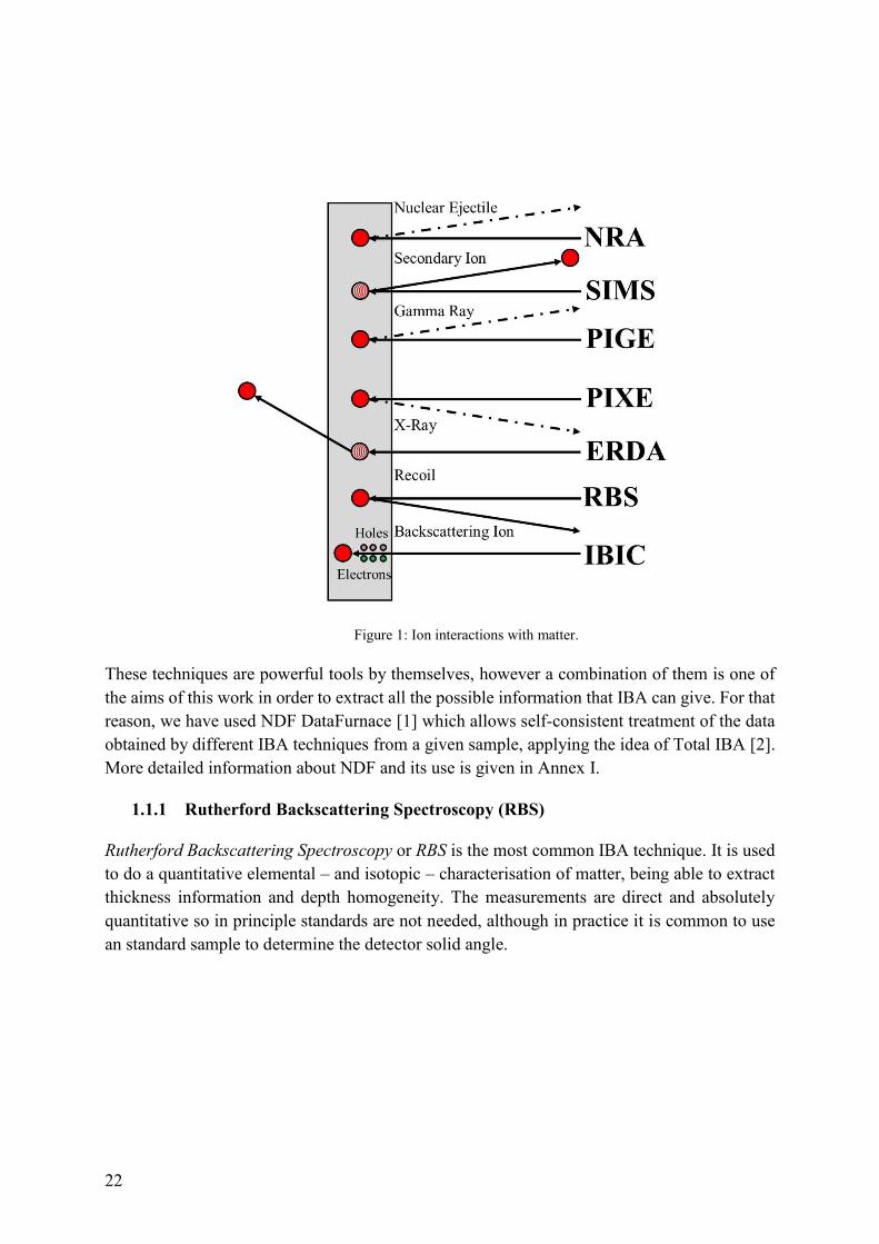
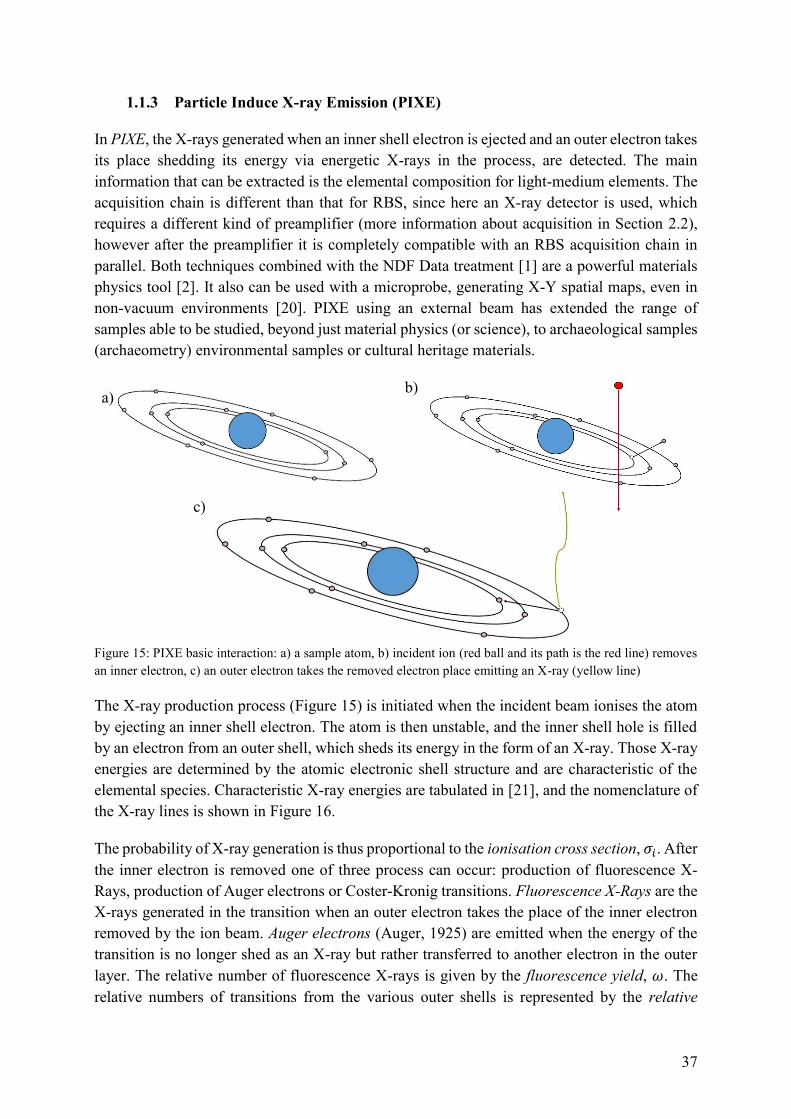
IBA techniques have been widely used for characterisation of materials from semiconductors to organic polymers since the 1970s since they provide direct and absolutely quantitative measurements in principle without the use of standards The energy of the scattered incident beam particles recoiled particles or nuclear reaction events provides information on the atomic or nuclear species that has interacted with incident beam The number of detected interaction products (for a given incident beam fluence) provides information on the concentration of the target nucleus or atomic species and in cases where the detected particle also loses energy traversing the solid target the energy spectrum also provides information on the depth distribution of the target nucleus Figure 1 shows a summary of the possible ion-matter interactions which are encompassed by IBA
Rutherford Backscattering Spectrometry (RBS) where the fundamental event is elastic backscattering of the incident ion Light ions at medium energies (05-25 MeV) are the most commonly used since at higher energies the cross section is no longer Rutherford although the interaction remains elastic (in this case the term EBS Elastic Backscattering Spectrometry is often used in the literature) It is interesting for medium and heavy target elements Z~(8 90) Depth profiles can be extracted Medium Energy Ion Scattering (MEIS) is a variant of RBS in which an electrostatic detector under ultra-high vacuum is used to improve energy (and hence depth) resolution The best depth resolution is obtained with ions near the maximum of the stopping power curve ndash around 100 keV for protons and 400 keV for 4He+
21
In Elastic Recoil Detection Analysis (ERDA) a target particle recoiled by the beam is detected The incident ion has to be chosen according to the target element with typical incident energies in the range 2-100 MeV Depth profiles can be extracted
Particle Induced X-ray Emission (PIXE) where the x-rays resulting from the interactions between the atomic shell electrons and the ion beam are collected Light incident ions are used at medium energies (1-3 MeV) It is used to study light-medium elements Z~(11-60) No depth profile can be extracted
Particle Induced Gamma-ray Emission (PIGE) is similar to PIXE but using the gamma rays generated in ion-nucleus interactions Light ions at medium energies (1-3 MeV) are used It is used for light element identification Z~(3-20) Depth profiles can be obtained when the cross section has narrow resonant structures by scanning the incident beam energy in the vicinity of the resonant structure In this case the method is referred to as Narrow Resonance Profiling (NRP)
In Secondary Ion Mass Spectrometry (SIMS) the target components are sputtered by the ion beam and they are classified according to their mass using a mass spectrometer It is interesting for surface characterisation giving nanometre scale depth profile Typically heavy ions of energies in the range 2 keV to 20 keV are used since the required instrumentation is at a modest scales and sputtering yields are sufficient
In Nuclear Reaction Analysis (NRA) charged particles or gamma rays resulting from nuclear reactions with the ion beam are detected Because nuclear reaction cross sections generally vary quite strongly with ion energy and detection angle the incident ion its energy and the detection angle have to be chosen according to the element being analysed for example carbon can be detected using a deuterium beam at 12 MeV where the reaction 12C(dp0)13C will take place giving a proton as a residual ejected particle If as is most conveniently the case the nuclear reaction is exothermic then the elastically scattered primary beam can be stopped by a mylar (Polyethylene terephthalate) film that is still thin enough to allow passage of the higher energy nuclear reaction products Depth profiles can be extracted
Ion Beam Induced Charge (IBIC) Unlike the above ion beam techniques IBIC is not an elemental materials characterisation but rather a tool to study the electronic behaviour within a material It is used for wide bandgap materials such as semiconductors junction (p-n Schottky) insulators and semi-insulators materials It has a great interest to measure and map transport properties such as carrier concentration mobility and lifetime diffusion processes depletion region thickness the charge collection efficiencies and charge drift length as well as lattice dislocations point or extended defects and radiation induced damage
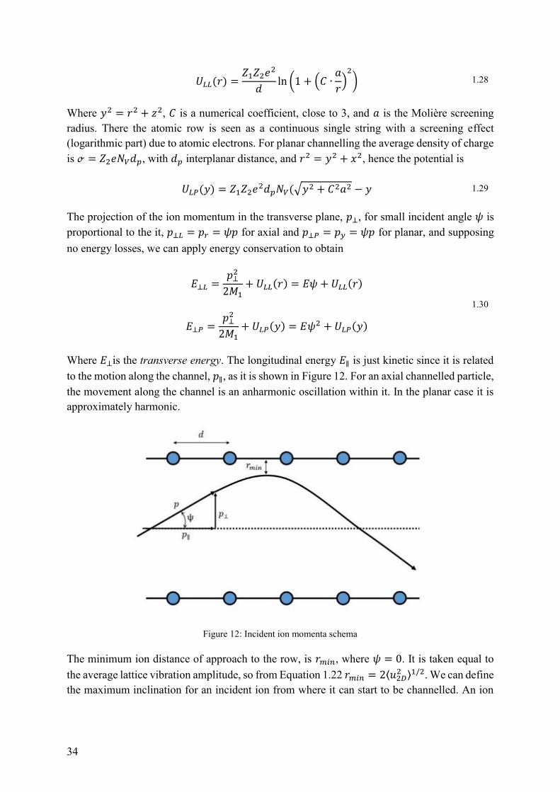
The techniques used in this thesis (RBS PIXE NRA and IBIC) will be presented in more detail in next subsections Channelling (subsection 112) is not mentioned above since it is not an extra technique but a different experimental configuration of the other techniques
22
Figure 1 Ion interactions with matter
These techniques are powerful tools by themselves however a combination of them is one of the aims of this work in order to extract all the possible information that IBA can give For that reason we have used NDF DataFurnace [1] which allows self-consistent treatment of the data obtained by different IBA techniques from a given sample applying the idea of Total IBA [2] More detailed information about NDF and its use is given in Annex I
111 Rutherford Backscattering Spectroscopy (RBS)
Rutherford Backscattering Spectroscopy or RBS is the most common IBA technique It is used to do a quantitative elemental ndash and isotopic ndash characterisation of matter being able to extract thickness information and depth homogeneity The measurements are direct and absolutely quantitative so in principle standards are not needed although in practice it is common to use an standard sample to determine the detector solid angle
23
0 200 400 600 800 1000 1200 1400
0
200
400
600
800
1000
Yield
Yie
ld (
Co
un
ts)
Energy (keV)
Bismuth Signal
Silicon Signal
Figure 2 RBS (4He+ - 1500 keV normal incident beam at 165deg scattering angle) spectra of bismuth thin film (peak between 1300-1350 keV) on silicon substrate (lower energy up to 800 keV)
The backscattering ions arrive at the particle detector where their energy is deposited giving rise to a charge pulse of magnitude proportional to the ion energy for each ion Charged particle detector operation is presented in more detail in Chapter 2 A typical RBS energy spectrum is shown in Figure 2 The backscattered particle energy depends on the elastic collision with the target nucleus and the energy lost along the path (ingoing and outgoing) inside the sample mainly due to collisions with electrons The probability for an incident particle to be backscattered is given by the Rutherford Backscattering Cross Section (σ)
Figure 3 Schema elastic collision Where 119864012 is energy 11987212 mass and 119907012 velocity for the incident particle and target while 120579 and 120601 are angles in the laboratory frame
The incident ion energy are at relatively low energy (500-5000 keV) ie it is a non-relativistic system and therefore the interaction between incident ion and target nuclei is a classical mechanics elastic collision In Figure 3 is represented the simple elastic two-body collision which is expressed as the conservation of energy and momentum
1198640 = 1198641 + 1198642 rArr
1
211987211199070
2 =1
211987211199071
2 +1
211987221199072
2 11
24
0 = 1 + 2 rArr
11987211199070 = 11987211199071 cos 120579 + 11987221199072 cos1206010 = 11987211199071 sin 120579 + 11987221199072 sin120601
12
Through the equation 11 and 12 is obtained
11990711199070= (
(11987222 minus1198721
2 sin2 120579)12 +1198721 cos 120579
1198722 +1198721) rArr 13
⟹11986411198640= (
(11987222 minus1198721
2 sin2 120579)12 +1198721 cos 120579
1198722 +1198721)
2
equiv 119870 14
Where K is known as Kinematic factor
Figure 4 Three elementcompound (119860 119861 119862) thin layers on thick layer substrate target incident and backscattered ion beam ∆119864 = 1198640 minus 119864119899=119860119861119862hellip
However the incident particle penetrates into the sample losing some energy until the particle-nuclei collision occurs (Figure 4) The Stopping Power d119864119889119909 which represents the average energy loss per unit length is the physical quantity to take this fact into account Here it is convenient to introduce the concept of stopping cross section 119904 which is simply the stopping power per atom It has two different components 1) due to the electronic cloud (electronic stopping power) and 2) related to the nuclear collision (nuclear stopping power) The electronic stopping power is an inelastic interaction due to generation of plasmons (collective electron excitations) and single ion-electron (localised) interactions The equation 15 Bethe (1930) established an approximation taking into account the first order quantum perturbation and non-relativistic velocities [3] which can give us a fairly accurate estimate
119904119890 =1
119873
d119864
119889119909|119890=41205871198851
211989041198731198852
11989811989011990712 ln
211989811989011990712
119868 15
Where 119868 is the target averaged ionisation potential ndash since this process is ionising the matter along the incident particle pathndash which can be taken from experimental data or calculated by dipolar oscillator forces as was done by Bloch (1933) [4]
25
On the other hand the nuclear stopping is related to the elastic interaction with the atom which has much lower cross section Nevertheless the implications for the incident ion path can be very important It is responsible for the ion scattering in any direction ndash including the backscattering process which is the main interaction in RBS ndash changing the trajectory dramatically Here the interaction is coulombian ndash it is a non-ionising interaction ndash but the electrons which are bound to the nucleus cannot be ignored since they may screen the nuclear charge from the ion Screening corrections to the Rutherford cross section are introduced by Ziegler (1988) [5] Andersen (1980) [6] or LrsquoEcuyer [7] to cite just three The sn values are tabulated using experimental data or may be calculated by computer simulation methods such as the widely used semiempirical binary collision approximation (TRIMSRIM [8]) and less used molecular dynamics simulation [9]
Figure 5 Example of electronic stopping power using the Bethe formula for incident high energetic 4He+ in Ni [10]
In the non-relativistic regime 119904 = 119904119890 + 119904119899 rArrd119864
119889119909=d119864
119889119909|119890+d119864
119889119909|119899
where the stronger term is 119904119890
due to the higher number of interaction (assuming SRIM for 2 MeV alpha ion beam (4He+) in Ni 119904119890= 6192 keVmicrom and 119904119899= 07 keVmicrom) Assuming that d119864119889119909 is known for a given target and incident ion type and energy an energy-depth relationship is established in Equation 16
119909119899 = int (
119889119864
119889119909)minus1
1198891198641198640
119899=119860119861119862hellip
= (1198640 minus 119864) (119889119864
119889119909)minus1
|119899
16
Where 119899 is the average energy 119899 =1
2(119864119899 + 1198640) 119899 being each elementcompound When a
film is composed of a mix of element 119860119894 in proportions 119886119894 so that the composition is 1198601119886111986021198862hellip with sum 119886119894 = 1119894 the Bragg rule of linear additivity may be applied to estimate the compound stopping power 119904119888 from the elemental stopping powers 119904119894
119904119888 =sum119886119894119894
119904119894 17
It is the basic relationship between the energy and the depth which makes RBS a powerful technique in films characterisation and material science
26
The energy loss is the result of a large number of energy loss events between the particle and the electrons of the solid (here we ignore the nuclear contribution which is negligible for the light ions and energies used in RBS) The number of such interactions follows a Poisson distribution and in each event the energy lost follows a probability distribution These two probability distributions thus lead to variations in the actual energy lost for each ion traversing a given material thickness This is called energy straggling and we denote the distribution for the loss of energy 119906 after traversing a thickness x of matter by 119892(119906 119909) In the cases encountered here 119892(119906 119909) may be assumed to follow a Guassian distribution of which the standard deviation 120590119892 may be estimated from
120590119892 = Ωradic119909 18
Where Ω is termed the straggling constant The straggling constant may be estimated theoretically although good measurements are more reliable then the theoretical estimates Bohr (ref) derived the straggling constant for the idealised case of free electrons to be ΩB = 885 keV(mgcm2)12 If elemental straggling constants are known they may be linearly combined with an analogie of the Bragg rule for stopping powers
Focusing in the ion-nucleus interaction we have seen that the amount of energy transferred (kinematics) is shown in Equation 14 and the interaction is through Coulomb potential (with screening correction) We now consider the frequency of these interactions ndash ie their differential scattering cross section 119889120590119889Ω which takes in account both the Rutherford scattering cross section5 (120590) and the detector solid angle (Ω) Equation 18 shows the expression where 119873 is the number of atoms per cmsup2 in the target 119909 is the target thickness 119873119894 number of incident particles 11988512 incident and target atomic number and 119890 is normalised electron charge6
119889120590
119889Ω=1
119873119909((119889119873119894119889Ω)
119873119894) = 19
5 Lord Ernest Rutherford (1871-1937) used a classical coulomb interaction to describe in 1911 [104] the backscattered alpha particles observed by his students Hans Geiger and Ernest Marsden in 1909 [105] and thus he gave us the first proof of the atomic nucleus In the Geiger-Marsden experiment a radium alpha source was placed in front of foils of several materials and they measured the scintillations produced by the backscattered alpha particles in a zinc sulphide screen They observed a very small number of these backscattered particles compared with the transmitted and lightly deflected particles and further noted an increase in the alpha yield from targets of larger atomic number and from thicker foils Rutherford explained this fact by a positive-positive repulsion due to coulomb force which could be just possible if a very small positive charged zone were in the atoms of the foils contrary to the Thomson model which supposed a great positive ball with small negative zones within it The Rutherford model was improved by Niels Bohr in 1913 taking in account quantum mechanics [18 19 20] giving the Rutherford-Bohr atomic model well implanted nowadays 6Throughout this thesis we use 1198902 = 119902119890
2
41205871205760= 144 119896119890119881 119888119898 = 144 119890119881 Aring where 119902119890 is the electron charge
27
= (11988511198852119890
2
2119864119894)
24
sin4 120579 [1 minus ((
11987211198722) sin 120579)
2
]
12
+ cos 120579
2
[1 minus ((11987211198722) sin 120579)
2
]
12
110
This equation can be simplified when 1198721 ≪ 1198722 giving Equation 111
119889120590
119889Ωasymp (
119885111988521198902
2119864119894)
2
[sinminus4120579
2minus 2 (
11987211198722)2
] 111
This statistics of the number of detected particles follows a Poisson distribution since the probability cross section is small and the events are independent The standard deviation of a Poisson distribution is the square root of the mean and this uncertainty limits the precision with which an RBS measurement may be performed For example to determine the area of a peak to within 1 precision requires at least 10000 events to have been recorded in the peak
Finally a schematic RBS system is shown is Figure 6 Here the detected particles are the backscattered ones hence the 120579 is large (between 140deg to 170deg) in order to get the maximum which is led by the cross section The total number of detected particles (119873119889) is expressed in Equation 112 where 120572 is the incident beam angle
119873119889 =
120590Ω ∙ 119873119894 ∙ 119873119909
cos 120572 112
Figure 6 a) General RBS schema the incident ion beam impact with the sample (target) and ions are backscattered to the detector with a frequency given by 119889120590119889Ω b) incident beam zone in target beam surface 119878 and 119909 is penetration distance 119873 is the number of atoms per unit volume
28
112 Channelling
The next IBA configuration introduced is Channelling Actually channelling is a phenomenon that can occur for any IBA technique however we are going to present just the RBS case ndash in which the sample holder is installed on a goniometer in order to align the ion beam with an axis or plane of a monocrystalline material It is a powerful technique to study crystalline material surfaces lattice order and non-ionising ion damage (see Annex II Ion Damage) Unlike diffraction techniques ndash X-Rays or electrons ndash channelling is the result of highly local interactions and is best described in real space Explanations about the physical behaviour in this configuration will be done below
Figure 7 GaAs atomic structure a) in random configuration b) channelled in axis lt0 0 1gt c) channelled in axis lt1 0 1gt and d) plane [0 0 1]
In a non-channelled single crystal RBS measurement the sample has to be oriented well away from any major crystalline axis or plane so that all the incident ions can see all the atoms in the sample with the same probability7 This configuration is called random and it is illustrated in
7 A perfect random is quite complicated to get and an accurate angle scan has to be done In practice a quick angle scan is enough and some channelling corrections are implanted in the offline data treatment
29
Figure 7a for GaAs When the ion is aligned with an axis (Figure 7b and c) or planes (Figure 7d) we are in the channelling configuration
1121 Surface peak
Figure 8 Scattering interaction between ion and first atomic layer
The ion flux is uniform and there is no shadowing for the first atomic layer and so this layer always contributes fully to the backscattering yield By considering the deflections from the ions in the first and successive layers we can estimate the probabilities of scattering from the successive atomic layers Let us first consider just the surface atomic layer As in RBS the interaction channelling is ruled by the Coulomb force hence the incident ions will be scattered with an angle 120593 (Figure 8) where the momentum difference is
Δ119901 = 21198721119907 sin (
1
2120593) 113
And
Δ119901 = int119865 cos(ϑ) 119889119905 = int
119885111988521198902
1199032cos(ϑ)119889120599 (
119889119905
119889120599) 114
Using the angular momentum conservation we can write 119903 as a function of 120599
1198721119903
2119889120599
119889119905= 1198721119907119887 ⟹ 1199032 = 119907119887
119889119905
119889120599 115
Substituting in Equation 114 and changing 120599 = 120593
2+120587
2 we obtain
Δ119901 = int
119885111988521198902
119907119887cos (120593 minus
120587
2) 119889120593 =
2 119885111988521198902
119907119887cos (
120593
2) 116
The combination of 113 and 116 gives
tan120593
2=2 11988511198852119890
2
11987211199072119887=11988511198852119890
2
2119864119894119887 117
30
Where 119864119894 is the incident ion kinetic energy Further in the ion trajectory the ion will interact with the second atom along the atomic row which is a distance 119889 from the first one The ion position there is expressed as
1199032 = 119887 + 120593119889 118
In the Equation 117 we found an expression for the scattering angle as a function of the impact parameter 1198878 It is reasonable assume that the angle 120593 is small enough to consider that tan120593 asymp120593 therefore Equation 118 can be rewritten as
1199032 = 119887 +
119885111988521198902119889
119864119887 119
Thus a shadowing effect is generated with cylindrical symmetry due to the first atom as is shown in Figure 9 It is possible to calculate the radius for this shadow cone (119877119862) through the 1199032 minimum
1198891199032119889119887|119877119862
= 0 ⟹ 119877119862 = radic4119885111988521198902119889
119864 120
The shadow cone will generate a forbidden zone which depends on the interatomic spacing along the row where no ion can penetrate and it is ultimately the cause of the surface peak existence It has a value of the order of 10-1 Aring
Furthermore we can also express the ion fluence distribution 119891(119887) as a function of incident fluence Φ0 and the impact parameter 119887
119891(119887) =
0
Φ0119887
119903
119889119887
119889119903
119903 lt 119877119862119903 gt 119877119862
121
8 This concept has been applied although not shown in the previous section about RBS It is included in the electronic stopping power the Rutherford cross section and straggling disertations
31
Figure 9 Incident ion fluence distribution in the two first layers
However the explanation above is just valid to have a qualitative idea of the channelling process in the material surface since there is not taken in account a) the vibrations of the atomic nucleus in a lattice where the amplitude is within 10-1 - 10-2 Aring hence it is close to the 119877119862 values and b) the screening corrections in the Coulomb force due to the atomic electrons
Thermal vibrations in crystalline solids can be explained by the Debye model [P Debye 1912] where there are three vibrations modes (one longitudinal and two transversals) in the Bravais lattice with frequency 120596lowast and state (modes) density associated 119892(120596lowast) [11] The probability density of these modes 120588 is ruled by Bose-Einstein statistics [S Bose 1920 and A Einstein 1924] and when the system is in thermodynamic equilibrium and in contact with a thermostat at temperature 119879 that density is expressed as a Gaussian [12] It can be projected on one random direction here will use 1199061119863 allowing us to have an analytical expression and extract the displacement average using the Debye-Waller factor 119882 [13] as follows
lang1199062rang12 =
3ℏ2
1198961198611198722Θ119863[1
4+
119879
Θ119863119882(
Θ119863
119879)]
12
122
Where the values (lang1199062rang12 = lang1199092rang12 = lang1199102rang12 = lang1199112rang12 or combinations) are between 005 and 02 Aring If lang1199062rang12 ≪ 119877119862 the ion path will not be perturbed by the second atom However if lang1199062rang12 asymp 119877119862 the ion will be likely scattered once again until the ion position 119903119894 where 119894 indicates the atom number or atomic layer if we are in 3-D where big enough in comparison with the lattice vibration displacement Thus channelling is a great technique to characterise material surfaces as we will see below9
9 Debye Model is convenient to have a first approximation understanding of the lattice vibration behaviour however it is not completely realistic since the displacements considered above are isotropic and axis independent but actually they are not Monte Carlo calculations are needed to take in account these correlated displacements
32
The screening effect will change the potential seen by the ion which will no longer be purely Coulomb so the angle 120593 and 119877119862 calculations will be affected A reasonable correction but not unique is to apply the Thomas-Fermi Model (L Thomas and E Fermi 1927) for the atomic potential with the Moliegravere approximation (G Moliegravere 1947) where the potential is expressed as follows
119880119872(119903) =
119885111988521198902
119903(01119890minus
6119903119886 + 035119890minus
03119903119886 + 055119890minus
12119903119886 ) 123
Where 119886 is the Moliegravere screening radius which depends with the Bohrrsquos radius 1198860 as follows
119886 = 088531198860(1198851
12+ 1198852
12)minus23 1198851≪1198852 119864asymp1 119872119890119881
rarr 119886 = 088531198860(1198852)minus13 124
From here we obtain the Moliegravere Cone radius 119877119872 where 119877119872119877119862 ge 08 [14]
Once the corrections are applied the number of atoms per row can be calculated so a surface characterisation can be done The yield for the first two atoms will be given by the convolution of the ion fluence Equation 121 and the position distribution 119875(119903) which is a Gaussian function Unfortunately this convolution has no analytical solution further than the third atom in the row due the complexity of 119903119894(119887) when the corrections are included (Equation 118) To get analytical results Monte Carlo calculations have to be done obtaining the yield per atom in the row This is called Close Encounter Approximation [15] where the fluence uniform and perpendicular to the surface plane has a Dirac distribution with 120575(119899) for an incident particle 119899 giving a normalised yield of backscattering particles for one atom
120594 = sumint119891(119899)119875(119899)119889119899
120081
119899=1
= (2120587119873119881119889120081lang11990611198632 rang)minus1sum119890
minus|119899 |
2
2lang11990611198632 rang
120081
119899=1
125
Where 120081 is the number of interactions and 119873119881 the volumetric atomic density10 To note that an associated area with a radius 1198770 around the row can be defined which gives us a geometrical radial symmetry as
1205871198770
2 =1
119873119881119889 126
Extending 120594 for all the successive atoms indicated by 119895 we obtain an expression for the atoms per row 119871 which indicate the number of measured atoms in RBS-channelling corresponding to the material surface Some results are shown in [11 12]
10 There is expressed lang11990611198632 rang as the thermal vibrations in one dimension from here will be distinguish the vibration amplitude depending the degrees of freedom
33
119871 =sum120594119895
infin
119895=1
127
From the experimental point of view it is measured by the areal integration of the surface peak subtracting a triangle which base is the line between the peak centre (119864119901) and the minimum energy peak (119864119872) and the height is the yield in 119864119872 as it is shown in Figure 10 The limit in the measurement is given by the detector resolution (see Subsection 211)
Figure 10 RBS-Channelling spectrum for 2 MeV He+ ion beam on Pt lt1 1 0gt axis Striped area corresponds to the atoms in the surface [16]
1122 Beyond the surface peak
The above description involves the first atomic layers (~5 nm) where the characteristic surface peak is created After that the ion propagates through the crystal via the interatomic row channels This was described by Lindhard [17] using quasi continuum potential 119880119871(119903) along the atomic rows known as Continuum Model instead of the binary interaction
Figure 11 Channelling geometries a) axial channelling where the axis z generates the linear potential in the ion M1 and b) planar channelling where the plane x-z generates the planar potential in M1
Channelling can be done in two geometries axial and planar (Figure 11) For axial channelling the continuum potential is written by
119864119872 119864119901
120594(119864119872)
34
119880119871119871(119903) =
119885111988521198902
119889ln (1 + (119862 ∙
119886
119903)2
) 128
Where 1199102 = 1199032 + 1199112 119862 is a numerical coefficient close to 3 and 119886 is the Moliegravere screening radius There the atomic row is seen as a continuous single string with a screening effect (logarithmic part) due to atomic electrons For planar channelling the average density of charge is ℴ = 1198852119890119873119881119889119901 with 119889119901 interplanar distance and 1199032 = 1199102 + 1199092 hence the potential is
119880119871119875(119910) = 119885111988521198902119889119901119873119881(radic1199102 + 11986221198862 minus 119910 129
The projection of the ion momentum in the transverse plane 119901perp for small incident angle 120595 is proportional to the it 119901perp119871 = 119901119903 = 120595119901 for axial and 119901perp119875 = 119901119910 = 120595119901 for planar and supposing no energy losses we can apply energy conservation to obtain
119864perp119871 =
119901perp2
21198721+ 119880119871119871(119903) = 119864120595 + 119880119871119871(119903)
119864perp119875 =119901perp2
21198721+ 119880119871119875(119910) = 119864120595
2 + 119880119871119875(119910)
130
Where 119864perpis the transverse energy The longitudinal energy 119864∥ is just kinetic since it is related to the motion along the channel 119901∥ as it is shown in Figure 12 For an axial channelled particle the movement along the channel is an anharmonic oscillation within it In the planar case it is approximately harmonic
Figure 12 Incident ion momenta schema
The minimum ion distance of approach to the row is 119903119898119894119899 where 120595 = 0 It is taken equal to the average lattice vibration amplitude so from Equation 122 119903119898119894119899 = 2lang11990621198632 rang12 We can define the maximum inclination for an incident ion from where it can start to be channelled An ion
35
has a potential 119880119871 = 0 just before it interacts with the sample therefore applying the transverse energy conservation through Equation 130
119864119894119899119888119894119889119890119899119905 = 119864119903119898119894119899 ⟹ 119864ψc2 = 119880119871(119903119898119894119899)
ψc = radic119885111988521198902
119864119889ln [1 + (
119862119886
119903119898119894119899)2
] =ψ1
radic2ln [1 + (
119862119886
119903119898119894119899)2
]
12
131
Which is called the critical incident angle If 120595 gt ψc channelling will not happen Also we define ψ1 as the critical angle in the first order approximation for light and fast ions Doing an analogue procedure for planar channelling equation 132 is obtained
ψc = radic
2120587119873119881119889119901119885111988521198902
119864[(lang1199102rang + 11986221198862)12 minus lang1199102rang12] 132
Experimentally the measurement of the critical angle is made through the close encounter probability yield as function of the incident angle measured by the goniometer 120594(120595) There we have to take the angular width at the half minimum ψ12 ie 120594(ψ12) = 12 as is shown in Figure 13 In the figure we can note a normalized yield higher than 1 in the wings of the angular distribution This is because of the higher fluence around the rows which generates a bigger scattering contribution Critical angles calculated this way overestimate measured values by about 15 [14] which is rather good given the various approximations that we have used Due to the dependence with 119889 the critical angle can be used to define the lattice structure of the sample
Figure 13 Yield as function of the incident angle 120594(120595) for 480 keV protons on W crystal along lt1 0 0gt axis [14]
To complete the channelling parametrisation is necessary to introduce the definition of minimum yield It is the physical quantity which will give the amount of disorder and corresponds to the minimum backscattered particle yield within the interatomic row channels
120594(ψ12) = 12
2ψ12
36
In axial geometry the reference [14] shows that for a parallel incident ion (120595 = 0) with a fluence 119891(119903) and position distribution 119875(119903) ndash analogue to Equation 125 ndash the minimum yield 120594119898119894119899 is
120594119898119894119899(120595 = 0) = int 119891(119903)119875(119903)119889119903 =
1198770
0
int ln (11987702
11987702 minus 1199032
) sdot119903
lang11990621198632 rang119890minus
1199032
2lang11990621198632 rang 119889119903 =
1198770
0
=lang11990621198632 rang
11987702 = 2lang1199062119863
2 rang119873119881120587119889
133
In an experiment this parameter can be measured integrating an energy window in the RBS channelling spectrum just before the surface peak on the bulk zone and dividing the area by the random spectrum area in same window ie 120594119898119894119899
119890119909119901 = 120594119888ℎ119886120594119903119889119898
Experimental measurements give an underestimation of factor of about 3 in comparison with the calculations A correction to solve this deviation based on numerical simulations using the Moliegravere potential without continuum model or transverse energy conservation was introduced by Barrett (JH Barrett 1971) It is shown in [15]
The minimum yield provides us a lot of information about crystal quality The minimum yield may increase due to dechannelling which depends on the thermal vibrations and electronic stopping power ndash and is therefore present even in an ideal monocrystal ndash as well as the displaced atoms due to defects Defects can be localised such as interstitial atoms or extended such as dislocations stacking faults or amorphous zones Characterising the dechannelling effects can give remarkable information (qualitative and quantitative) about the crystal structure Furthermore channelling effects can also occur for the outgoing particle If the detector is placed at an angle corresponding to a major axis or plane (Figure 14) then the yield is further reduced due to blocking effects In the case of dual channelling and blocking alignment the number of backscattered particles further decreases and the minimum yield is reduced quadratically 120594119898119894119899119863119906119886119897 = 120594119898119894119899
2
Figure 14 ion beam and particle detector aligned with two different crystal axis to generate the blocking effect
More detailed information and examples can be found in [16] [18] [19]
37
113 Particle Induce X-ray Emission (PIXE)
In PIXE the X-rays generated when an inner shell electron is ejected and an outer electron takes its place shedding its energy via energetic X-rays in the process are detected The main information that can be extracted is the elemental composition for light-medium elements The acquisition chain is different than that for RBS since here an X-ray detector is used which requires a different kind of preamplifier (more information about acquisition in Section 22) however after the preamplifier it is completely compatible with an RBS acquisition chain in parallel Both techniques combined with the NDF Data treatment [1] are a powerful materials physics tool [2] It also can be used with a microprobe generating X-Y spatial maps even in non-vacuum environments [20] PIXE using an external beam has extended the range of samples able to be studied beyond just material physics (or science) to archaeological samples (archaeometry) environmental samples or cultural heritage materials
a) b)
c)
Figure 15 PIXE basic interaction a) a sample atom b) incident ion (red ball and its path is the red line) removes an inner electron c) an outer electron takes the removed electron place emitting an X-ray (yellow line)
The X-ray production process (Figure 15) is initiated when the incident beam ionises the atom by ejecting an inner shell electron The atom is then unstable and the inner shell hole is filled by an electron from an outer shell which sheds its energy in the form of an X-ray Those X-ray energies are determined by the atomic electronic shell structure and are characteristic of the elemental species Characteristic X-ray energies are tabulated in [21] and the nomenclature of the X-ray lines is shown in Figure 16
The probability of X-ray generation is thus proportional to the ionisation cross section 120590119894 After the inner electron is removed one of three process can occur production of fluorescence X-Rays production of Auger electrons or Coster-Kronig transitions Fluorescence X-Rays are the X-rays generated in the transition when an outer electron takes the place of the inner electron removed by the ion beam Auger electrons (Auger 1925) are emitted when the energy of the transition is no longer shed as an X-ray but rather transferred to another electron in the outer layer The relative number of fluorescence X-rays is given by the fluorescence yield 120596 The relative numbers of transitions from the various outer shells is represented by the relative
38
transition probability 119896 There can also be subshell transitions between outer shells These are called Coster-Kronig transitions (Coster and Kronig 1935) and these probabilities are represented by branching fractions 119887
Figure 16 Atomic x-rays transmission
There are some models for protons in K transitions [22]ndash[25] however when the subshells appear the theory becomes very complicated and the results have to be constrained with the empirical data [26]ndash[29] Anyway the next transitions (M Nhellip) are not so useful for PIXE since they overlap in the spectra and the uncertainly becomes difficult to manage
The X-ray background is quite different to the particle background in RBS In RBS it is due to the backscattered ions which go deep in the substrate In contrast for PIXE it is mainly due to the bremsstrahlung effect This effect occurs as a result of the momentum changes of the incident ions and ejected secondary electrons This is the source of one of the big advantages of PIXE over electron beam induced fluorescence Protons are some 2000 times heavier than electrons and so they suffer much less violent deceleration as they slowdown in the target producing orders of magnitude less bremsstrahlung background since its cross section depends inversely on the mass square Eventually another source of background is the gamma rays emitted in nuclear reactions The cross section of these background contributions is complicated to model ndash but there are some fair attempts [30] ndash therefore is necessary to use experimental data to supress it properly in the later analysis The ejected electrons and secondary electrons generated by the ion beam are further sources of Bremsstrahlung The three main contributions are Quasi-Free-Electron bremsstrahlung (QFEB) Secondary-Electron Bermsstrahlung (SEB) and Atomic Bermsstrahlung (BA) In QFEB the ions have high speed in comparison with the atomic electrons hence they can be considered as free electrons Their energy distribution is then given by classical kinematics and their spectrum contribution is at low energy (~1 119896119890119881) but with high intensity The SEB occurs when the ejected electron losses energy through
39
Coulomb scattering within the target This Coulomb interaction places the background signal in the medium part of the energy spectrum (~5 119896119890119881) with also medium intensity The AB in other hand occurs when the electron comes back to the initial state The contribution is across the whole PIXE energy spectrum but with a very low intensity
The detector characterisation has to be done carefully in PIXE ndash here it is more critical than in RBS A typical X-ray detector is the lithium drifted silicon (Si(Li)) which is a p-i-n diode of around 5 mm thickness The i-type layer (insulator) is there in order to avoid high acceptor concentration This detector has to be cooled down typically to liquid nitrogen temperature and biased at high voltage (-1000 V) A thin ohmic contact film is on the surface (To check dead layer concept see Subsection 115 and Section 2 below) A thin window usually made of beryllium (tens of micrometre thickness) is needed to avoid backscattered ions reaching the detector and inducing damage and interfering with the X-ray detection In some cases if the studied elements are heavy in a light elemental matrix for instance an absorber is placed to eliminate the lower energetic X-rays where the bremsstrahlung background is higher Often two detectors are used with different windows allowing optimal detection of both light and heavy elements Detailed knowledge of the window thicknesses and composition dead layer and detector active zone thickness is necessary for reliable data analysis since the detector efficiency 120598 depends on these elements [31]
Equation 134 describes the number of arriving X-rays in to the detector where 119905 is the absorber transmission factor 119860 atomic mass 119873119886119907 Avogadrorsquos number 119873 target element concentration and 119879(119864) transmission factor related to the detector remaining components have been presented above However this equation is strictly valid for the two first X-ray lines (K and L) and does not take in account the secondary fluorescence
119873119863 =
119873119886119907 120596 119887 119905 120598 (Ω4120587)119873119868 119873
119860int
120590119894(119864)119879(119864)119889119864
119878(119864)
119864119891
1198640
134
The usual PIXE spectra are treated with fitting tools (such as GUPIX [32] [33] or GeoPIXE [34]) which can subtract the background and the pile-up to convert the peak spectrum areas in elemental concentration More information about PIXE and applications are in [16] [31]
114 Nuclear Reaction Analysis (NRA)
NRA is a technique which uses the exothermic nuclear reaction products to characterise target elements The nuclear interaction here is neither elastic nor analytically described since it is ruled by quantum nuclear mechanics [35] The instrumentation is very similar to that used for RBS and it is a technique complementary to those explained above since the nuclear reaction cross sections primarily exist for light elements that cannot be measured otherwise It is possible to include NRA data in NDF and thus to extend the self-consistent analysis to RBS PIXE and NRA measurements (see Annex I NDF DataFurnace and Total IBA)
The incident ion overcomes the nuclear coulomb barrier and interacts with the nuclei via nuclear potentials The ion excites the nucleus breaking the nuclear bonds and producing new elements
40
or isotopes These may either be in the nuclear ground state or in an excited state eg 28Si(2H+H0
+)29Si where 29Si nuclei are the ground state while in 28Si(2H+H1+)29Si the 29Si atoms
finish in the first excited nuclear state Mass is not necessarily conserved The energy consumed or produced in the reaction is labelled 119876 so that 119876 = [(1198721 +1198722) minus (1198723 +1198724)]1198882 and the reaction may be exothermic (119876 gt 0) or endothermic (119876 lt 0) The residual ejected particle (usually the light reaction product) energy is measured by the charged particle detector (Figure 17)
Figure 17 Ion-Nucleus reaction scheme for 18O(H+4He+)15N Yellow balls are neutrons and protons are red ones This reaction is exothermic with a Q=39799 keV
The cross section is no longer Rutherford rather it is a non-analytical cross section with values up to 103 times smaller than the Rutherford and hence NRA uses high ion fluxes in comparison to RBS with typical ion current and beam spot around 200 nA and 2 mm diameter respectively The NRA cross section has to be treated through the nuclear forces which due to their quantum nature cannot be analytically described Nevertheless there is a great experimental database provided by International Atomic Energy Agency (IAEA) constantly updated (IBANDL httpswww-ndsiaeaorgexforibandlhtm) Moreover a semi-empiric cross section code SigmaCalc is available with reliable and useful results [36] Nevertheless there are some common features with the RBS ndash EBS ndash that makes easier to understand and manage the information given by this technique The particles detected follow the same Equation 112 as the RBS does The stopping power has to be treated in the same way since the nature of the ions is essentially the same
NRA usually uses the light particle (proton deuterium or alpha) produced in the nuclear reaction For high Q values this particle can have much higher energy than the backscattered particle measured in RBS previously shown Particles with this amount of energy generate longer ionisation path within the detector that may be larger than the depletion zone thickness (see next Subsection 115 and 211) and the particle charge incompletely collected
41
Furthermore due to the high incident ion flux the backscattered ions can overload the data acquisition and so a foil of thickness sufficient to stop the backscattered particles but thin enough to transmit the higher energy nuclear reaction products (5 to 50 microm) is placed in front of the detector In exchange we obtain an extra stopping power contribution and the depth resolution is deteriorated This configuration is called Non-Resonant NRA and it is very convenient to quantitatively characterise light elements or isotopes which cannot be measured with RBS In the other hand Resonant NRA is the best to measure depth profiles of those light elements Resonant NRA uses nuclear resonances at certain energy eg 629 keV 18O(H+4He0
+)15N and varying the incident ion energy the depth profile can be obtained [37] [38]
Further NRA experimental setup information and physic explanation are in [16] [39]
115 Ion Beam Induction Charge (IBIC)
Contrasting with the above IBA techniques in IBIC the measurements are not done through an outgoing reaction product after the sample interaction In IBIC the information source is the charge generated by the ion beam within the sample and the electronic signal that is created is the output The experimental setup changes since an ion microprobe is needed in order to have small beam currents (~fA) in a well located zones within the sample The beam may be scanned to generate X-Y maps of the IBIC signals
Figure 18 Charge induction schema The ion creates the electron-hole pair which is instantly broken through the electric field and an inducted charge is generated The signal is amplified and converted to voltage signal through a charge sensitive preamplifier
The ion-matter interactions explained in Subsection 111 are also valid here however we are going to focus on the electronic response of the sample itself so the output is obtained from the sample directly no detector being needed As we saw the electronic stopping power decreases the ion energy until either the particle is backscattered from a nucleus (RBS NRA) or it comes to rest in the sample When an energetic ion travels through the matter it generates a charge track in which a great number of electron-hole pairs (EHP) is created [40] The energy required to create one electron-hole pair in a semiconductor is directly related to the material energy gap eg 36 eV for silicon at 300 K (around 3 times the energy gap) and it is independent on the ion characteristics After there is a relaxation time as known as recombination in which the neutrality comes back Also some carriers can be trapped in the material defects which is called
42
trapping contributing to increase the relaxation time When a potential difference is applied an electric field within the material is generated (Figure 18) and the EHP generated breaks away and a charge is induced However the dielectric relaxation time in semiconductors is smaller than the carrier lifetime ie the recombination ndash combining with trapping ndash process is very quick so there is no time to induce charge by the carriers The induced charge by EHP can be measured just when the material is in the relaxation regime [41] The relaxation regime is reached in the wide bandgap materials or semiconductor junctions where the potential difference applied in the material terminals produce a behaviour like a capacitor Here the carrier movement can be treated electrostatically due to their low speed The potential difference is called bias voltage and it generates the active zone called depletion zone (119909119889) in which the electrostatic field is generated This will be treated in more detail in Section 21
The canonical example which is used here too is a pn semiconductor junction There a highly doped semiconductor is in contact with a lightly oppositely doped one (high n and light p or vice versa) This is basically the structure of a typical charged particle detector which will be explained in Subsection 211 The main interaction here is the charge induced by the incident ion which is governed according to the ShockleyndashRamo theorem (W Shockley 1938 [42] and S Ramo 1939 [43]) which was generalised by Gunn [44] There the general expression for an induced charge and its current are given by
119868119894 = minus119902 ∙
120597(119903)
120597119881119894 135
∆119876119894 = 119890(
120597Υ(119903)
120597119881119894|119903119891
minus120597Υ(119903)
120597119881119894|1199030
) 136
Where is the moving charge velocity 120597(119903)120597119881119894 is the weighting field 120597Υ(119903)120597119881119894 is the weighting potential for the electrode 119894 and 119902 is the electron charge (119903) and Υ(119903) represent the external electric field and potential From there we can see that the induced charge just depends on the initial and final position of the carrier In the case illustrated in the Figure 18 parallel plate model we can rewrite 135 and 136 as
∆119876 = 119890∆119909
119889=
minus1198901199090119889
⟼ electrons
119890(1199090 minus 119889)
119889 ⟼ holes
137
119894 = 119890
119907(119905)
119889 138
In the RBS explanation (Subsection 111) the relationship between the ion path and the energy through the stopping power was shown Here it is the same process the induced charge depends on the ion path and it is related to the energy deposited using the stopping power However it is an ideal case since the lifetime of the carriers and the possible trapping processes which can
43
occur are not considered We thus introduce the charge collection efficiency (CCE) concept in order to define the real charge collected versus the charge induced [45] Therefore the energy measured in the detector 119864119889 can be written as
119864119889 = int 119862119862119864(119909)
119889119864
119889119909119889119909
1199090
0
139
Where 119862119862119864(119909) can be experimentaly calculated dividing the detected energetic pulse by the incident energy The integral is defined between x=0 when the ion enters in the material and 1199090 where the ion has come to rest This is also an ideal case due to the fact that the highly doped zone in the top andor the ohmic contact produces a so called dead layer in which the stopping power is different A realistic mathematical treatment has to also take this into account From the experimental point of view the output signal is given as a voltage 119881119889 which is scaled into an energy using the electron-hole creation energy (119864119890ℎ) and the preamplifier feedback capacitance (119862)
119864119889 =
119881119889119864119890ℎ119862
119902 140
If the ion has a range greater than the depth of the depletion region recombination can occur in the non-depleted region Then the diffusion length (119871) of the material plays a special role It contains the average time of the free carriers lifetime and the diffusion coefficient [20] The equation 139 becomes into
119864119889 = int 119862119862119864(119909)
119889119864
119889119909119889119909
119909119889
0
+int 119862119862119864(119909)119889119864
119889119909expminus(
119909 minus 119909119889119871
)1198891199091199090
119909119889
141
For IBIC with light ions the inherent damage due to the beam (see Annex II Ion Damage) is reduced since the range in the sample can be long without a great amount of energy On the other hand using heavy ions the sample suffers more ionisation damage in a smaller depth However the contrast in an X-Y scan map is higher since the charge deposited is bigger and more sensitive to potential CCE defects Charge funnelling which is the increase in deposited charge and the higher localisation due to the plasma track generated by the incident ion [46] is greater when the ion mass gets bigger so its effects may become significant when we are using heavy ions
12 Topological Insulators (TI)
The first attempt to apply our segmented detector was for analysis of a three-dimensional Topological Insulator (TI) material A TI is an electronic state of the matter which presents an insulatorsemiconductor behaviour in the volume (bulk band) but a conductive nature on the surfaces Furthermore these conductive surfaces have the property to confine the electron movement in just two different senses (Figure 19) This is due to the special surface electronic band present in these sort of materials TI are closely related to the Quantum Spin Hall Effect
44
(QSH) ndash actually a material with QSH is a two-dimensional TI11 ndash which is the effect to have the integer quantum Hall effect without an external magnetic field It was predicted by F Duncan M Haldane [47] and finally theorised by CL Kane and EJ Mele [48] in that case for the graphene Both kind of materials TI and QSH have a topological invariant (Chern invariant) which ensures that the system stays in the same state under Time-Reversal (TR) perturbation ie topological states are very robust under smooth changes such as atomic structure defects [49]
Figure 19 A Topological Insulator has an insulator behaviour in the bulk (purple) and conductive beaviour on the surfaces (yellow) the electron movement there is fixed in two senses depending on the electron spin
The bulk electronic band is a trivial insulator (or semiconductor) however the surface electronic band is a gapless Dirac cone kind with massless Dirac fermion carriers within which generates the quantum state called Topological Surface State (TSS) as shown in Figure 20 It is similar to the graphene structure but with an even number of these cones whereas in the TI are an odd number [49] There the electrons spin-momentum vector is locked therefore the linear movement is spin dependent restricting the carrier conduction to just two directions That is called helicity and it happens because the spin-orbit coupling of the atomic outer shell electrons generates a band inversion through overlapping conduction and valence bands producing TR symmetric states In comparison with graphene the TI states are less dependent on atomic structure offering a more tuneable material to be used for example in spintronic technology
Inducing a perturbation in the TSS which breaks the TR symmetry such as external electricmagnetic field or ferromagnetic impurities on the surface the Dirac cone can be opened There the interchange between TSS and ferromagnetic states is crucial for possible applications not just in spintronic technology [50] but exotic quantum phenomena or fundamental particle physics as well [51]ndash[53] Here is where the RBS with a large solid angle segmented detector can be useful since the small amount of ferromagnetic doping may be directly measured with lower uncertainty using the same measurement time (deeper explanations about Segmented Detector in Subsection 212)
11 In order to have a more confortable read TI along this thesis is refered to three-dimension topological insulators
45
Figure 20 Topological insulators band structure The bulk contribution (blue) is a trivial insulator while the Topologic Surface States (TSS) are a gapless Dirac cone (red lines) with spin-orbit locked massless Dirac fermions
The TI compound used is the Bi2Se3 due to the simplicity in its band structure (just one Dirac cone) and the electronic properties which make it functional at ambient temperature with a 03 eV energy gap [54] The atomic structure is based on a rhomboidal unit cell with 5 atoms The Bi and Se atoms are intercalated within Quintuple Layers (QL) along the z direction and bonded by Van der Waals forces [55] as is represented in Figure 21
Figure 21 Bi2Se3 atomic lattice structure
The Van der Waals forces are weaker than other kind of bounds (such as ionic or covalent bonds) therefore the Bi2Se3 may be damaged easily with an ion beam so it is good candidate
46
to be studied with a large solid angle detector which reduces the beam fluence needed (and thus the incident ion damage) to obtain spectra of given statistics (also see more in Subsection 212)
Chapter 3 presents the work done on the elemental characterisation of the Bi2Se3 (as deposited and Fe-containing) and the related publications
13 Organic Semiconductor Devices
Optoelectronics has been an interesting topic in the last decades and when is combined with organic semiconductor technology the scope is huge in terms of future sustainable development with multiple applications such as organic photovoltaic solar cells organic electronic and optoelectronic devices or gas and chemical sensors They would have a big impact in multiple fields from the conventional use technology (eco-friendly electronic devices) to medical diagnosis (malignant corps detection in the body) However some issues related with the intrinsic properties of these kinds of materials have to be overcome such as low conductivity and carrier mobility or instability under environmental condition Deeper research about the physicochemical behaviour of these materials and their combination with inorganic compounds have been ongoing in many research groups for years [56]
The semiconductor behaviour in organic materials arises from the 120587 and 120587lowast (bonding and antibonding) molecular orbitals which are generated by the pz component in the sp2 atomic orbitals The bonding 120587 orbital represent the Highest Occupied Molecular Orbital (HOMO) whereas the antibonding is the Lowest Unoccupied Molecular Orbital (LUMO) These orbitals can be understood as conduction band HOMO and valence band LUMO making an analogy with the inorganic semiconductors However energy gap between them is quite big to be considered as a semiconductor material (2-5 eV) and the carrier mobility is low (1 cmsup2 V-1 s-1) therefore a certain amount of charge has to be injected (or extracted) to turn this insulator behaviour into a useful semiconductor That can be done by molecular doping as well as layer junction with carrier exchange properties [57]
Transition Metal Oxides (TMO) have been demonstrated as great charge exchangers for organic semiconductor technologies due to their electronic structure where the strong orbit-orbit interaction generates unusual orbital filling which leads to interesting carrier transport properties since they have deep uncompleted atomic orbitals The TMO reduces the hole extraction barrier through its Work Function (WF)12 and the organic molecule Ionisation Energy (IE)13 [58] [59] Nevertheless there is a limitation the WF of TMO varies with the stoichiometry therefore there is a dependency with any stoichiometric change eg the external oxidation due to the environmental exposition which has to be well understood to have realistic chances generalising the use of organic semiconductor technology outside the academic world
12 Intrinsic characteristic of a solid material which represents the energy required to move an electron away from it 13 Energy required to remove a valence electron form a neutral atom
47
Two interesting applications involve the TMO and the organic compounds Organic Photovoltaic (OPV) using the TMO as a hole extractor and organic transistors light emitters chemical and gas sensors devices where the TMO has a hole injector role The OPV solar cell technology has a very promising future although nowadays the efficiency is around 11 quite lower compared with the 30 in thin film GaAs solar cells [60] the tendency is increasing since in the last years a big effort is being made by the scientific community and some public institutions However there are some underlying aspects that need to be understood in order to describe the physics of the organic semiconductor and to improve manufacturing processes The organic (or hybrid organicinorganic) devices are promising to slow down ndash or even stop ndash the extreme semiconductor dependency decreasing costs and power consumption in the same time as the detrimental potential residues are also reduced In any case the charge exchangers are needed to overcome the conduction limitations given by the organic compounds the thermal stability and the reliability under real environmental conditions are key to make these materials an available replacement for the hydrocarbon-based energy or inorganic electronic devices Figure 22 shows the layout for an OPV based on TMO MoOx
Figure 22 OPV layout MoOx is the TMO working as a hole extractor for the DBP organic p-type semiconductor BCP Bathocuproine is the electron extractor for the Fullerene C60 n-type organic semiconductor Au and ITO are the device anodecathode
Chapter 4 shows how we used the new enhanced charged particle detection system to study both materials In particular we have focused on the Tetraphenyldibenzoperiflanthene (DBP) which has been demonstrated as a good organic semiconductor donor [61] [62] and the binary compound MoOx as a good candidate as hole injectorextractor for the organic devices via HOMO level [58] Here we present IBA measurements of the oxidation process in the TMO MoOx with different stoichiometryrsquos which is extremely important for the WF controlled tuning and therefore for the charge exchange process Moreover we demonstrate the capabilities of the Segmented Detector in the organic compound measuring the DBP carbon quantity using IBA techniques
48
2 Charged Particle Detection
One of the central preoccupations of this thesis is the instrumentation used for IBA since it has been a great improvement in the particle detection and data acquisition Therefore a complete description concerning physical principles and our remarkable enhancements are necessary to have a general point of view about these two topics in IBA techniques Section 21 is about semiconductor charged particle detectors explaining how they work (Subsection 211) and which were the developments reached during this thesis Segmented Detector (SegDet) characterisation and installation at SAFIR (Subsection 212) The study of charge collection efficiency in our detector is presented in the manuscript NIMB_PROCEEDINGS-D-16-00174 which was presented at the 12th European Conference on Accelerators in Applied Research and Technology (ECAART) and is submitted for publication A proposed design for an annular segmented detector is presented in Section 213
Section 22 presents the data acquisition systems which involves the signal amplification (Subsection 221) and the pulse processing after the charge collection is explained in Subsection 222 with an explanation of the different parts in the acquisition chains for both the old fashion analogue method and the digital system as well as a comparison between them
21 Semiconductor Detectors
The semiconductors charged particle detectors have been widely used during the second half of the 20th century Firstly in early 1960s they were made from commercial germanium diodes (thin Surface Barrier detector) and they were mainly dedicated to nuclear physics the hottest topic in those days They replaced the Gas Ionisation Chambers used until then These semiconductor solid state detectors provided a great advantage in comparison with ionisation chambers due to enhancement in energy resolution and the possibility to reduce the size since the studied particles are stopped at shorter distance and larger energy loss increasing thus the sensitivity
Rapidly in the late 1960s the germanium was replaced with silicon since the former had to be cooled to keep the leakage current low while the silicon properties ndash larger energy gap ndash made it possible to work at room temperature It was also possible to build light-proof detectors depositing an aluminium thin film on the surface giving the possibility to study particles within a lighted environment Such detectors were installed in the Voyager spacecraft (launched in 1977) to study cosmic rays outside the solar system (and it is still acquiring data)
These detectors were used for nuclear or fundamental physics mainly gamma rays and charged particles coming from nuclear reactions In 1970s two facts made possible and extremely convenient the use of the charged particle detector to IBA for material science On one side the semiconductor technology development increased dramatically with better and cheaper semiconductor detectors and electronic devices and on the other side the nuclear processes knowledge within the materials was good enough to start to apply this knowledge in the material description and characterisation Furthermore the nuclear and particle physicists could not use any more those ldquosmallrdquo particle accelerators since to continue their works higher energies were
49
necessary therefore the conversion of those facilities into material and solid state physics was as natural as needed
This development has been keeping until now improving resolution packaging size data acquisition systems etc going from the great ATLAS detector in CERN to tiny low-cost p-i-n detectors
211 Single Detector
Different techniques and materials are used to build up semiconductor detectors however we will focus on Passivated Implanted Planar Silicon (PIPS) detectors since they have optimal characteristics (price resolution size) and are now the most commonly used These detectors are based on a semiconductor silicon wafer (p or n type) doped by ion implantation technique on the front andor back side with p or n ion species hence letting free holes or electrons in order to make a p-n junction (Figure 23a) The thickness is typically from 200 to 1000 microm and the surface area from 25 to up to 1200 mm2 When a reverse bias voltage is applied ndash hence an ohmic contact or high carrier density has to be added on both detector sides ndash an electric field is created perpendicular to the wafer plane surface direction This electric field generates a depletion region or active zone in which free electrons in the conduction band go from the p type into n type material and holes go into n type from the p type so they are all are matched within the electric field as is shown in Figure 23b
Figure 23 On the left p-n junction schema On the right reverse bias applied in p-n junction
Therefore detectors could be understood as capacitors and its behaviour is governed the well-known equation 21
119862 = 휀
119860
120596119889 21
Where 휀 is the dielectric constant (in Si 휀 = 119휀0 where 휀0 is the vacuum permittivity) 119860 is detector surface area and 120596119889 is depletion layer thickness This layer is the active part of a detector with thickness that can be controlled through the applied reverse bias voltage The depletion thickness can be calculated by
50
120596119889 = radic
2휀(119881119887 + 119881prime)
119890 ∙ 119899= radic2휀120583120588(119881119887 + 119881prime) 22
where 119899 micro and 120588 are carrier number mobility and resistivity respectively We can approximate all of them to silicon wafer type carrier so as to simplify Note as well that 119881119887 is reverse bias voltage 119881rsquo is intrinsic potential difference due to p-n junction14 and 119890 is electron charge
Figure 24 Electron-hole generation through the ion path due to ionising excitation
In this state the carriers are in equilibrium with no free electrons or holes When a charged particle enters within this zone the equilibrium can be broken if the energy is enough and excites the valence electrons Those excited electrons can jump to the conduction band generating then free electron-holes pairs as is represented in Figure 2415 Once an electron-hole pair is produced an induced charge 119902 is generated within the electric field due to the Shockley-Ramo theorem [63] as was explained in Subsection 115 Thus the relationship between energy deposited and signal size is given by Equation 23
119902119904 =
119864
119864119894119902119890 23
Where 119902119904 is average induced signal charge 119864 deposited energy 119864119894 energy required to ionise the atoms in the semiconductor and create electron-hole pair (36 eV for silicon) and 119902119890 is the electron charge After a pair is produced and the signal is created this has to be amplified and digitally treated in order to extract a spectrum in the computer These following steps will be explained below in Section 22
However there exists some elements which perturb the simple physics explained above Firstly the incident particle has to pass through the ohmic or highly doped front contact essential for the charge collection where energy will be lost without ionisation resulting in a shift in the 14 In the p-n junction without any external applied voltage carriers are diffused thermally and electrons and holes can be matched just where p and n zone are touching (Figure 23a) therefore there exists an intrinsic depletion zone 15 Description of how a detector works is valid for all kind of semiconductor detectors
51
energy spectrum This generates the so called dead layer Furthermore some of the particles will be backscattered from the detector atoms To take into account these corrections for non-ionizing energy loss a Pulse-Height Defect (PHD) model [64] has been successfully developed and widely used
Several considerations must be made to give a full account of the performance of the charge collector ie compromise between energy resolution and number of collected events The energy resolution equation with all the contributions would be as is shown in Equation 24 where the terms are statistically independent
Δ119864 = radicΔ119864119890119897119890119888
2 + Δ1198641199041199051198861199052 + Δ119864119862119862119871
2 + Δ1198641198891198972 + Δ119864119896119894119899 + Δ119864119904119910119904 24
The very first contribution is the electronic noise (∆119864119890119897119890119888) The electronic noise is an addition of two main contributions electronic and thermal fluctuations The source of them in the detectors are the leakage current and the capacitance in the p-n junction because the detector is working as a non-ideal capacitor and there they both have a detector surface dependence [65]
∆119864119890119897119890119888 prop radic119868119863(119860) + 119862119863
2(119860) 25
Another important contribution to the energy resolution is the statistical fluctuation of the number of electron-hole pairs created (∆119864119904119905119886119905) ie intrinsic energy uncertainty due to statistical processes involved in the charge collection The incident ions are statistically independent and their interactions can be expressed with Poisson statistics however although every ion loses exactly all of its energy in the detector the fluctuations in the number of charge pairs produced deviates from the Poisson distribution This is taken into account via the Fano factor [66] which accounts for loses ending up in secondary e-h pairs created by the primary ones which interact with the phonon modes [67] [68] Thus the fluctuations in the measured energy for given incident energy (119864) can be expressed as function of the Fano factor (119865) and the material ionisation energy (119864119868) and it is independent of the incident ion nature
Δ119864119904119905119886119905 = 235 ∙ radic119865119864119864119868 26
Charge collection losses (∆119864119862119862119871) are due to the carrier trapping by detector crystal bulk (silicon) impurities The dead layer (∆119864119889119897) is a non-active area on the detector surface which is due to the ohmic surface contact and the entrance window (highly doped top layer) where a certain amount of energy is lost For a commercial PIPS detector-preamplifier system16 in standard conditions (with 50 mm2 of area and 400 microm of depletion zone capacitance asymp 13 pF leakage current asymp 20 nA at room temperature17) the energy resolution is around 15 keV
16 Preamplifiers will be discuss in Section 22 17 Values taken from the widely used Ortec silicon PIPS detector data sheet
52
Figure 25 Angle spread schema 120579 is the backscattering angle and Δ120579 = 120579119891 minus 120579119894 is the detector window width
The geometrical system has a contribution to take in account since there is an angular spread for a given backscattering angle due to the detector window width which is called kinematic spread (∆119864119896119894119899) In Figure 25 the range of possible backscattering angles is represented by Δ120579 The mathematical expression is based on the Rutherford backscattering cross section variation with the energy at different angles and assuming a Gaussian energy distribution It is expressed by Equation 27 where 120579119894 and 120579119891 are the extreme angles for a given detector and the summation has to be done taking angle steps between them
∆119864119896119894119899(120579) =
= 235 ∙ sum radic119864(120579) minus sum 119864(120579prime)((120590(120579prime)120590(120579119894)
) ∙ (119864120579prime+1 minus 119864120579prime)
sum (120590(120579)120590(120579primeprime119894)
) ∙ (119864120579119894primeprime+120579119894+1
primeprime minus 119864120579119894primeprime)
120579119891
120579primeprime=120579119894
)
minus1120579119891
120579prime=120579119894
∙
120579119891
120579=120579119894
∙ radic(120590(120579)
120590(120579119894)) ∙ (119864120579+1 minus 119864120579)
27
Also the environmental system conditions are a noise source (∆119864119904119910119904) (hard to measure and control such as microphonic vibrations environmental signals etc)
Furthermore when two simultaneous particles arrive at the same time the charge induced will be the addition of the real particle charges and these two events will be counted as one There exists both on-line and off-line methods to suppress or simulate this phenomena Below in Section 22 the experimental and analytical treatment solutions will be presented
212 Segmented Detector
In this thesis a large solid angle Segmented Detector (SegDet) has been used in order to improve the performance of a typical single PIPS detector (Figure 26) It was designed and built within the European project SPIRIT however was modified and improved during the SPRITE project in which this thesis is undertaken
53
Figure 26 SegDet appearance a) SegDet and housing schema b) SegDet and print circuit picture c) SegDet completely mounted
There are several reasons to develop and use a large solid angle segmented detector in ion beam analysis techniques Firstly a large solid increases the counts number for a given incident ion fluence The solid angle is proportional to the surface area of the detector A ruled by
Ω =
119860
1199032 28
Where 119903 is the distance between the sample and the detector The number of particles detected 119873119889 is proportional to the solid angle as is shown in Equation 112 In our case the detector surface active area is 763 mm2 In comparison with a 50 mm2 detector using a 8x2 mm2 collimator in front of it to avoid kinematic spread (it is a classical RBS detector configuration) a SegDet segment is more than 3 times bigger solid angle and the total SegDet is more than 48 times therefore the number of detected particles is augmented and statistics improved for a given beam fluence However the bigger surface area reduces the energy resolution due to the electronic component (both leakage current and capacitance depend on the area) the kinematic spread (larger backscattering angle range) and the pile-up (simultaneous events) The optimal way to keep the large solid angle avoiding those problems is segmenting the detector In our case the detector was longitudinally divided in 16 side-to-side segments (29x164 mmsup2) Furthermore use of several backscattering angles helps solve the intrinsic mass-energy ambiguity typical for IBA18 A Guard Ring (GR) at the same voltage as the detector bias surrounds the segments to isolate them keeping the leakage current low thus the edge current is captured and the impedance reduced In Figure 27 are shown the GR and interstrip region structure The segmentation multiplies the data measured but also the system to get this data the well-established analogue system cannot face the 16 acquisition channels in a cheap and comfortable way Section 22 contains the approach used to acquire data with the SegDet
18 The energy can be lost by two factors elastic collision (119870) and stopping power (119904) In a single IBA experiment is not possible to discern between them however using several backscattering angles 119870 will change since it depends on the angle while 119904 remains the same In NRA the energy tranfer is not elastic but the principle is the equivalent
Main housing piece
Grid
Isolating plastic
SegDet Board
54
Figure 27 Guard Ring and interstrip region microscopic view (left) and a cross section schema (right)
The direct implication of the statistical improvement keeping an optimal resolution conditions is the possibility to study samples with small quantity of matter such as small peaks of light elements built on the background signal or heavy elements with small intensity Another enhancement using our SegDet is the damage reduction to the sample due to the incident beam An ion beam are accelerated charged particles therefore they are irradiating all around their path Also interactions between beam ions and sample atoms (both electrons and nucleus) create defects in the materials even more when these materials are conductors or semiconductors with crystallised structures or insulators such as organic tissues With the SegDet we are able to analyse these kind of fragile materials under ion beam Further explanations about damage induced by ion beams are in Annex II Ion Damage
In the following Subsubsection 2121 is a paper submitted as ECAART 12th proceedings in which is presented the SegDet characterisation (leakage current and depletion thickness) focusing on the interstrip behaviour responses for the Charge Collection Efficiency (CCE) and the role of the GR in the detection system
The initial detector housing design inherited from the EC project SPIRIT was not completely installed in the vacuum chamber therefore it was not tested under real experimental conditions The detector grounding has to be properly chosen since such a big detector generates some undesirable antenna behaviour which produces parasitic noise Moreover the board where the detector is mounted and the preamp connection is made was not made in the cleanest way and constituted an extra noise source The changes that were made extra information about the detector characterisation ndash non-included in the article ndash and first results using several segments simultaneously are shown in Subsection 2122 Moreover the large solid angle can give the possibility to perform very low fluence experiment such as 4He2+ beam up to 4 MeV in small single ended accelerators such as the SAFIR facility which has 2 MV maximum terminal voltage corresponding to 2 MeV 4He+ in classical operation Some results of this operational mode are shown in Subsection 2122 as well
Active zone
Active zone
SiO2 SiO2
Guard Ring
55
2121 Charge Collection Efficiency Publication I
56
57
58
59
60
61
62
63
64
65
66
67
68
2122 Segmented Detector first results
In the Subsection above is shown the results presented and published however during this thesis more work has been done in order to increase and improve the knowledge about these kind of detectors In Figure 28 is represented the segment organisation and nomenclature in the SegDet
S 8 S 7 S 6 S 5 S 4 S 3 S 2 S 1
S 9 S 10 S 11 S 12 S 13 S 14 S 15 S 16
Figure 28 Segment organisation within SegDet
Previously to the detector installation in the experimental vacuum chamber and in order to understand better the operational behaviour and optimize its benefits some tests were done in the electronic workshop Using a pulse generator and under ambient pressure the energy resolution and its dependence with the GR configuration was measured In Figure 29 are represented six different configurations that were used everything floating (EF) studied segment biased (Bias) studied segment biased while the two side segments are biased as well (B+2S) studied segment floating and GR biased (GR) studied segment and GR biased at same voltage (Bias+GR) and studied segment and GR and two sides segments biased (B+GR+2S) Using these configurations we could measure the resolution without either any source of environmental noise dead layer shift or uncontrolled experimental perturbation since the effect of the pulse generator unlike a real ion has just the electronic noise contribution of the Equation 24 The uncertainties are those due to the capacitor tolerance (20) in the preamplifier test input Through that capacitance we are able to convert the pulse voltage in energy19 Also the uncertainty in the measured voltage (40plusmn1 mV) is taken in account The bias voltage used was -40 V the response is the same as for any other voltage after -5 V where the depletion region is already sufficiently thick that detector capacitance is no longer the limit to energy resolution
The results give us an idea of how the electric field is confined in the SegDet and applied voltage role In the figure is shown the great GR impact in which the energy resolution is even lower than in just the segment biased (20 keV for bias versus 15 keV in GR) That is because no e-h pairs are created and the charge induced is purely collected the only important factor here is the leakage current and detector capacitance The best configurations are bias and GR with the
19The conversion follows 119864 = 119864119894119881119862
119902119890 where 119864119894 is the energy needed for the e-h pair 119881 is the input voltage 119862 the
preamp test input capacitance and 119902119890 the electron charge In this case 119864 = 1350 plusmn 300 keV
69
same polarisation and bias GR and two adjacent side segments with the same polarisation both are equivalent with 10 keV energy resolution
16 1 4 9 8 12
0
5
10
15
20
25
30
35
40
45
50
En
erg
y R
eso
lutio
n (
ke
V)
Channels
EF
Bias
B+2S
GR
Bias+GR
B+GR+2S
Figure 29 Segment energy resolution for several segment and guard ring configurations in the SegDet using a pulse generator and -40 V bias voltage The uncertainty bars represent the uncertainty in the capacitance for the charge injection and the uncertainty in the size of the voltage step applied to generate the charge The non-shown segments were not available due to broken gold wire connection
Once the preliminary test were done we installed the detector (with all the housing components shown in Figure 26a) in a vacuum chamber without beam using a pulse generator instead The detector-preamp output signal was incredibly noisy due to the housing electrical shielding and poor detector board connectivity A new board was designed and built applying the experience gained in the experimental environment (we designed the board and it was built by Nolam Embedded Systems) The metallic (brass) detector housing can be understood as an antenna therefore the possible electromagnetic noise in the experimental environment could generate interferences in the detector signal This can be avoided improving the electronic shielding through a better grounding choice It has to be done carefully since for a good beam fluence measurement the chamber and the housing have to be connected between them and isolated from any other part On the other hand the detector itself has to be completely isolated (if not the signal would not be generated) the figure shows the plastic isolating piece which makes an electrical barrier between the detector and the grid The grid was designed to protect the thin gold wires (which make the connection for the bias and the output signal) as well as to separate the segments The publication above demonstrates that the grid is not needed for segment separation instead it can create unwanted scattering effects in the strip edges and generate spectrum distortions20 Therefore the grid was replaced by a brass mask which covers
20 The incoming ion can collide and be scattered with the grid strip edge The result is particles with less energy (more yield in the low energy part of the spectrum) and even changes in the segment since the trajectory can be completely changed Moreover the shape and straightness in the strips is not homogeneous which is an extra complexity in a potential correction factor for these effects
70
the gold wires but with a 30x30 mmsup2 hole opened in the detector area For shielding reasons this mask has to be grounded with the detector and isolated from the rest of the housing
After the noise optimisation the detector was ready to be applied in a real experimental test Figure 30 shows an RBS experiment performed using 4 segments simultaneously using the preamplifiers and data acquisition explained below in this chapter (Section 22) on a SiO2 sample with a Carbon substrate We used a 4He+ beam at 800 keV incident energy The backscattering angle is referenced by the SegDet centre (between Segment 12 and 4 so called S12 and S4)
It is possible to observe the silicon (around 400 keV) and oxygen (around 250 keV) peaks with slight differences in energy in the left part of the figure where both angles S4 and S12 are very close (∆120579 = 12057911987812 minus 1205791198784 = 117deg) while the energy shift in the right part is more pronounced (∆120579 = 12057911987815 minus 1205791198788 = 184deg) There is also an extra peak just next to the substrate signal below 200 keV which corresponds to the carbon deposition from the beam due to the poor vacuum done during the measurements
100 200 300 400 500
0
2000
4000
6000
8000
10000
12000
14000
16000
Yie
ld
Energy (keV)
Segment 4
Segment 12
100 200 300 400 500
0
2000
4000
6000
8000
10000
12000
14000
16000
Yie
ld
Energy (keV)
Segment 8
Segment 15
Figure 30 spectra taken simultaneously from four segments of the SegDet Two from the centre segments (left red and black) and two far between each other (right blue and orange) RBS done using 4He+ at 800 keV on SiO2 on C substrate
The large solid angle opens the way to reach higher energy using double charged ions as commented above In our case SAFIR is a 2 MV High Voltage accelerator facility with 50 years of extraordinary service it is well-known in the community for the high beam current and energy stability Nevertheless the limitations in the terminal voltage limit the ion beam energy and thus excludes some interesting analytical possibilities This is the case for example for the EBS resonance at 305 MeV for alpha particles on oxygen 16O (4He 4He0) 16O that is widely used in in studies of oxidation processes
One possibility to reach such energies with a small single ended accelerator is to use the doubly charged ions generated in the RF ion source however the beam current of doubly charged ions from the source is some 102 to 103 times smaller than that of the singly charged ions ndash practically inexploitable for the traditional analysis systems Here the SegDet can be extremely helpful
71
since by increasing the solid angle the measurement becomes feasible in a reasonable experimental time Figure 31 shows bismuth on silicon substrate spectrum which was the first taken in SAFIR with a doubly charged alpha particle beam 4He2+ at 4 MeV using a 25 mmsup2 single PIPS detector with a 6x1 mmsup2 window in the front to avoid kinematic spread The spectrum acquisition time was 20 minutes From the known Bi areal density and a geometrical estimate of the detector solid angle the incident 4He+ beam fluence was estimated to be 064 microC (14 ionsnmsup2 in the 2 mm diameter beam spot)21 which implies a 4He+ beam current of about 530pA For an RBS experiment to give spectra with reasonable statistics typically about 5 microC (5 ionsnmsup2) is required to obtain adequate statistics and since here the measurement time was 20 minutes a manageable experiment with this configuration would take about three hours for each spectrum Although possible it is probably more efficient to find a higher energy accelerator on which to perform such measurements
0 400 800 1200 1600 2000 2400 2800 3200 3600 4000
0
50
100
150
200
250
Yie
ld
Energy (keV)
Figure 31 Bi (553 TFU) on Si substrate spectrum with a classical single PIPS detector (25mmsup2) for 4 MeV 4He2+ ion beam The signals up to 900 keV are HH+ beam contribution at 2 MeV which is mixed with 4He2+
Note that up to 900 keV the yield is 4 times bigger This is due to the HH+ molecules present in the ion source which have practically the same charge to mass ratio as the 4He2+ and thus almost the same trajectory in the magnetic field of the analysing magnet When the magnet and beamline elements are carefully tuned to avoid this contamination the 4He2+ beam current is reduced even further
Figure 32 shows 4 MeV RBS spectra obtained with SegDet for a thin alloy (AuAgCu) film on a carbon substrate and same beam configuration as before but with the magnet optimised to avoid the HH+ beam component Note that the carbon signal is 6 times higher than that expected for Rutherford scattering since that is the cross section increase for 4He in carbon at this higher energy There are two SegDet segments (S5 and S12) taken simultaneously during 30 minutes As was done above for the 4 MeV spectrum obtained with the PIPS detector we can calculate the incident beam fluence and the 4He++ current to be about 095 microC (21 ionsnmsup2) and 530 pA respectively The spectrum obtained even with just one segment is already readily exploitable and when the spectra are obtained simultaneously for all 16 segments equivalent information
21 The values here are just approximations taking the number of particles in the spectra and acquisition time
72
would be obtained in around 2 minutes To obtain this information with the standard PIPS detector would again take on the order of three hours
0 400 800 1200 1600 2000 2400 2800 3200 3600 4000
0
100
200
300
400
500
600
700 S12
Yie
ld
Energy (keV)
0 400 800 1200 1600 2000 2400 2800 3200 3600 4000
0
100
200
300
400
500
600
700
800 S5
Yie
ld
Figure 32 Au078Ag015Cu007 (377 TFU) on C substrate spectra from SegDet segment 5 on top and 12 on bottom for 4 MeV 4He2+ ion beam
213 Annular Detector
In a first approach to obtain even higher solid angles within the SPRITE project (Marie Curie Actions) an annular segmented detector has been designed in collaboration with HZDR Rosendorff22 The main structure is similar to that of the SEGDET which has been shown to operate well The main improvement from such a detector is the increase of the solid angle for Ion Beam Analysis (IBA) techniques based on charged particle detection (Rutherford Backscattering Spectroscopy RBS Nuclear Reaction Analysis NRA Elastic Recoil Detection Analysis ERDA etc) as was explained above Furthermore for backscattering techniques the proposed annular design allows a large backscattering angle since the beam passes through a hole in the centre of the detector (Figure 33) which is the optimal configuration because a detector with enlarged surface area can be used increasing the count rate The detector is divided into annular segments in order to keep the capacitance low which also keeps the electronic noise low as was shown above and to follow cylindrical symmetry As a segmented detector it can also of course resolve the mass depth ambiguity inherent in RBS spectra
22 Milestone 23 Develop design of annular segmented detector
73
Figure 33 RBS and annular segmented detector schema
The layout of the detector has to be carefully chosen As the detector capacitance and leakage current significantly influence the energy resolution the area of the single detector segments should kept low Furthermore it is important to minimize the kinematic spread due to the segment width where the backscattering angle covers a range ∆120579 between maximum and minimum values The detector energy resolution has been explained above (Subsection 211) For a commercial PIPS 50 mm2 detector at room temperature with a 400 microm of depletion zone (capacitance asymp 13 pF leakage current asymp 20 nA) and standard preamplifier system the typical energy resolution for the statistically independent contribution is around 10 keV23 In our design segment areas are 50 mm2 and 400 microm depletion layer (17 pF 15 nA) have been used hence here it is reasonable to expect an energy resolution of about 10 keV24 as well
The design presented here has been arrived at by imposing an energy resolution for the kinematic spread smaller than 4 keV for light elements such as silicon for which the kinematic spread is the greatest In most practical cases there are also other system contributions for the energy uncertainty which may be difficult to control since they are associated with the measurement system which is reasonably valued at 1 keV but which can be negligible in very low noise environments (for more details see Subsection 211) Therefore in our design the total energy resolution taking in account all the contributions is around 15 keV
23 Those values are based on the semiconductor PIPS detector Ortec data sheet 24 Electronic energy resolution is ∆119864119890119897119890119888 ~ radic119868119863 + 1198621198632 (Equation 25) Leakage current (119868119863) is smaller in our case than in the reference between 07 to 08 times The square capacitance in our case is between 15 to 2 times bigger Therefore the differences are radic07 and radic08 smaller for current and radic05 and radic1 bigger for capacitance hence is reasonable to consider no changes in these contributions in energy resolution
74
Figure 34 On the top-left is the annular detector design The detector active area is blue and the detector mounting boards with copper signal paths are grey On the top-right is a detector section on the PCB On the bottom is shown the proposed pattern for fabrication of 6 detector sectors in a 776 x 395 mm silicon wafer
The detector design is shown in Figure 34 where the detector is composed of 6 annular segments each divided into 5 sectors giving a total of 30 segments for the array Each segment is surrounded by a 280 microm wide guard ring zone with a 30 microm guard ring in order to confine the electric field in the vicinity of the detector edges [65] It is usually biased at the same voltage as the detector bias In Figure 35 is shown the guard ring structure
Figure 35 Interstrip schema guard ring and passivated zone Detector active areas are in left and right sides
75
For a normally incident beam and 70 mm between the target and the detector the backscattering angles (θ) go from 173deg to 159deg the complete area for the active zone is 250 mmsup2 and the total solid angle is 282 msr In Figure 35 are shown the specifications for the segments in each part
The five silicon sectors are independent and have to be mounted on a printed circuit board (PCB) The PCB schema front and back side is shown in the top of Figure 36 The front side is divided in insulator (in grey) and detector grounding zone (in orange) The grounding part is where the detector would be glued with silver paste It is covered with a cooper thin layer to have an ohmic contact There is also a pad-hole connection for the grounding between both sides In the back side of the PCB the pad-holes are connected between them in order to have a common ground
Table 1 Segment specifications R (max and min) is segment radius r is segment width and area is calculated for the segment from one of the 5 sectors The sold angle (Ω) of each segment is calculated for the segment from one of the 5 sectors for a target-detector distance of 70 mm
Segment θmax (deg) θmin (deg) Rmax (mm) Rmin (mm) r (mm) Ω (msr) 1 17348 16977 800 1263 463 988
2 16956 16698 1290 1618 328 969
3 16677 16471 1645 1914 269 949
4 1645 16276 1941 2173 232 931
5 16256 16102 2200 2407 207 913
6 16083 15946 2434 2623 189 895
To make the p-n junction 5∙1014 atomscm2 of boron (p-type) would be implanted into the wafer front side and 5∙1014 atomscm2 of phosphorus (n-type) would be implanted at 50 keV into the wafer back side Aluminium ohmic contacts are also required on both sides and a passivation oxide added around the guard ring in order to avoid current leakage at the edges [65]
The above detector design may be fabricated using standard semiconductor processing techniques (ion implantation lithography CVD etc) as was the case for the SPIRITSPRITE linear segmented detector array (Subsection 212)
76
Figure 36 On the top-left PCB front side where are the pad-hole connections in the insulator part (grey) ndash with geometrical dimensions ndash and cooper covered for the back detector side grounding On the top-right PCB back side with a common ground connection On the bottom Contact pad-hole schema for detector output signal input guard ring voltage and detector back side grounding connection
22 Signal Acquisition and Treatment
Once the SegDet is operative a proper procedure is needed to treat the signal that comes from it The typical IBA acquisition system is shown in Figure 37 it is composed by a preamplifier just after the detector signal shaping and digitalisation The standard method for shaping is a semi-Gaussian shape through an analogue signal amplifier and a digitisation after that [69] However in our system we used a digital shaping approach provided by CAEN SpA SPRITE partner25
25 VAD undertook a secondment (SPRITE Internship Mobility Partnerships (IMPs) at the main CAEN facility in Viareggio (Italy) during this PhD
77
Figure 37 Data acquisition system schema
221 Preamplifier
The charge Q induced in the detector by the passage of a charged particle is typically too small (~fC) to be directly digitised and must therefore undergo an initial analogue amplification This is accomplished with a charge sensitive preamplifier which is basically a linear current integrator with an operational amplifier (opamp) where the current signal is converted into a voltage step of height 119881119900given by
119881119900 = 119866
119876
119862119891 29
Where G is the opamp gain and 119862119891is the value of the feedback capacitor A preamplifier circuit schema is shown in Figure 38 The capacitor 119862119891 gets charged quickly ie short rise time after which the current has to pass by the feedback resistor 119877119891which discharges the capacitor slowly ie long decay time This approach minimizes the effect of noise in the detector signal The detector polarisation voltage is applied via a current-limiting resistor in the preamps The preamps is placed as close as possible to the detector and the packaging has to be kept small in order to minimize the cable capacitance and limit microphonic noise and environmental pickup
78
Figure 38 Preamplifier circuit Input detector voltage 119881119894 induced by the charge deposited and the output voltage 119881119900 would be prepared for the shaping 119877119891 and 119862119891 are the op amp positive feedback to increase de voltage and 119877119889 is the detector bias resistor
In our system 16 acquisition channels have to be available therefore two 8 channel preamplifiers were designed26 based on the Cremat CR110 hybrid preamplifier modules27 In The preamp board is shown in Figure 39a the detector polarisation is daisy chainable for multiple boards and provision is also made for applying the polarisation to the guard ring The power supply is also daisy-chainable and protected by pi-filters
Figure 39 a) INSP-Nolam preamp board picture b) Cremat CR-110 preamplifier
222 Data Acquisition from analogue to digital
2221 Analogue system
In the standard IBA experiment data acquisition is performed through a shaping amplifier (semi-Gaussian shape) and a peak sensing analogue-digital convertor The digitised pulse height signal is treated by a multichannel analyser installed in a computer which represents
26 in collaboration with Nolam Embedded Systems Creteil France 27 httpswwwfastcomteccomfwwwdatasheeampcr-110pdf
b) a)
79
these data as a histogram (see Figure 2 in Subsection 111) A diagram of such a signal treatment and acquisition system is shown in Figure 40
Figure 40 Analogue data acquisition system Red lines are the signal shape after each step The current integrator is used to measure the charge deposited the input comes from the chamber and the output goes to AD Converter
The first step post-preamplifier in the acquisition is the pulse shaper which mainly functions to smooth the sharp step signal coming from the preamp and to attenuate the noise effectively improving the signal-to-noise ratio through an optimised frequency filter The signal treatment can be considered in reciprocal space using the Fourier transformation It is based on high pass differentiator and low pass filters and an integrator (CR-RC) The convolution of both generates the semi-Gaussian signal The amplitude of this signal is proportional to the incoming ion energy CR and RC time constant parameters have to be optimised for the experiment since the noise bandwidth and signal amplitude are related to them The optimal configuration of differentiator time 120591119889119894119891 and the integrator time 120591119894119899119905 have to be equal 120591119889119894119891 = 120591119894119899119905 = 119879119901 Thus 119879119901 is the maximum output pulse value which is called shaping time or peaking time Increasing 119879119901 allows averaging over a greater time and so results in less noise and better resolution However increasing 119879119901 also increses the time window in which a second particle can arrive and interfere with the treatment of the signal from the first particule resulting in pulse pile-up meaning it is necessary to find the optimum compromise between noise attenuation and single event measurement In an extreme case the next event will be overlapping the first one to the extent that the pulse height of the composite event will be the sum of the heights of the two events Even choosing optimum time parameters pulse pile-up cannot be completely avoided and the amplifiershapers usually have further pile-up rejection circuit installed This feature uses fast electronics to identify piled up pulses and establishes a time window within which the ADC is inhibited (and thus contributes to the ADC deadtime) however pulses which arrive too
80
closely together to be identified as piled up cannot be rejected and the remaining pileup needs to treated in spectrum simulations [70] [71]
Three other parameters in the acquisition are important The threshold establishes the minimum pulse voltage height to be take into account as an event This will reduce the false signals due to the white noise (high frequency) It has to be fixed high enough to discriminate those possible false events but low enough to count the real incoming ions The second parameter is the baseline which sets the zero amplitude of the shaping amplifier restoring it just after each event and is crucial to have an accurate pulse height measurement The last one is the pole-zero tail cancelation which optimally damps the signal from the shaping amplifier through the use of an additional tuneable resistor so that the signal returns as rapidly as possible to zero without overshoot or undershoot
The last step in the chain is the peak sensing ADC which converts the pulse height into a digital signal which can be classified by the multichannel analyser obtaining the final histogram
The second part of the system is related to integrating the current of the incident ion beam The measured charge is proportional to the number of incident ions and then to the charge In our system the chamber acts as a faraday cup and so must be completely isolated from ground where the ions colliding with the sample (total incident ions 119873119894) are generating a current The current integrator outputs a pulses for each incremental amount of charge which may be counted
2222 Digital system
The analogue data acquisition has been used for decades since it has a great robustness and a quite reliable performance Usually the after-preamp equipment is in the control room powered by a NIM (Nuclear Instrument Module) power supply (22x48x27 cm 5 kg) Furthermore the cost per acquisition channel is very elevated (gt10keurochannel)
In our case we have been using the 16 segments SegDet so a standard data acquisition method would have a very high cost Instead we employ a Digital Pulse Processing ndash Pulse Height analysis (DPP-PHA) provided by CAEN Spa (Viareggio Italy) in the SAFIR facility There the external analogue amplifier and ADC are not necessary anymore since all the electronics after the preamp is within the digitiser box A diagram of the acquisition chain is shown in Figure 41
81
Figure 41 Digital acquisition system using the digitiser provided by CAEN SpA
In the digital approach the ADC is the first step after the preamplifier using a 14-bit 250MSamples flash ADC followed by a FPGA (Field-Programmable Gate Array) where the digital signal will be treated and prepared to be displayed in a PC From here the first advantages arise In our system we used two CAEN DT5725 modules which are very compact (20x20x5 cm) with 8 spectroscopy channels each Furthermore the price per channel including preamplifiers is less than 1keuro unachievable for the analogue systems where the price would be over 10 times more Further advantages are that all the event data may easily be recorded in list-mode for detailed off-line treatment and that all the acquisition settings can be easily saved and recalled
Figure 42 Digital signal treatment schema
The signal treatment within the DPP CAEN digitiser shown in Figure 42 starts in the flash ADC where the analogue signal coming from the preamp is digitalised After that a decimation filter is placed in order to rescale the time parameters if the signal is very slow Usually for IBA
82
applications it is not the case The next step are the filters one dedicated to timing and another for energy
In the timing branch a trigger and a time stamp are generated when an event comes There the noise will be reduced avoiding false pulses (smoothing factor and trigger threshold) due to high frequency noise and subtracting the baseline after the event to minimize the pile-up It is working like the CR-RC filter in the analogue system but with a bipolar treatment being actually a RC-CRsup2 filter The bipolar approach improves the event identification since the zero crossing is detected irrespective of the pulse amplitude The minimum time interval delay between two events may be set
The energy filter is where the digital CAEN approach differs most from the analogue Instead of a semi-Gaussian shaping trapezoid shaping is used [72] Here as with the analogue system the height of the shaped signal is proportional to the preamp pulse height The trapezoid timing is divided in three steps rise time (119879119877) flat top (119879119865119879) and fall time Fall and rise time (which are always equal) and the flat top width can be adjusted They have an analogous function to the pulse shaping time in the analogue shaping amp and therefore they have to be well chosen in order to optimize resolution and to avoid pile-up During (2119879119877 + 119879119865119879) if a second event arrives the pile-up rejecter will reject both pulses however these pulses can be counted as pile-up events and included in the dead time which was not possible in the analogue system The rejecter cannot function the case of two very close events (during the CR-RCsup2 filter time) and there will be a real pile-up event However there exist hold-off and live time correction settings which can be programmed to establish a no recording time after the trigger and avoid even these pile-up events
When this time (2119879119877 + 119879119865119879) finishes the baseline is restored over a programmable number of points If the decay time (analogous to pole zero in the analogue system) is properly set up the baseline restoration is perfect The amplitude between the baseline and the filtered signal at the peaking time is the actual measurement of the energy The trapezoid height will be obtained by averaging the trapezoid flat top over a programmable width (peak mean)
83
Figure 43 Signal stages during the treatment CAEN user manual picture
2223 Acquisition System comparison
The digital approach given by the DPP is the most promising acquisition system for our setup however it has to be tested and compared with the well-established analogue system in order to demonstrate at least equivalent performance With this aim we performed full RBS experiments including RBS-channelling using both acquisition systems It was reported as a part of the SPRITE project28 The experiments were performed at the ALTAIumlS tandem accelerator (Universiteacute de Namur UNAMUR Belgium) Since the objective was to test the acquisition system a standard RBS configuration was used with a Passivated Implanted Planar Silicon detector (PIPS) collimated to 1mm and placed at 165deg and standard Canberra preamplifier and bias power supply The analogue acquisition was the standard system used at the ALTAIumlS laboratory (as explained above) while for the digital acquisition we used CAEN DPP (model DT5724) with MCsup2A multichannel analyser software provided by that company The beam was 4He+ at 1500 keV The beam fluence was measured through a current integrator connected to the chamber as a faraday cup as usual and one of the DPP input channels was used to count the charge pulses providing then not just the beam charge value but a time stamp for each beam charge pulse Two samples were studied a bismuth thin layer (553middot1015 cm-2) implanted in silicon (classical RBS reference sample) and Bi2Se3 (Topological Insulator TI that will be treated below Chapter 3) epitaxially grown on GaAs capped with ZnSe and lightly doped with Fe
28 Milestone 22 Enhanced digital acquisition in collaboration with CAEN Spa
84
200 400 600 800 1000 1200 1400 1600
0
50
100
150
200
Yie
ld
Energy (keV)
Digital
Analoge
1340 1360 1380 1400 1420 1440
0
10
20
30
40
50
60
70
Yie
ld
Energy (keV)
Digital
Analoge
Figure 44 Bismuth on silicon substrate RBS spectra black line is the full digital acquisition spectrum whereas the red line is the classical analogue one On the left is shown the spectra overview on the right the zoom in the Bi peak
The Figure 44 shows the digital and analogue normalised29 spectra taken on the BiSi sample Equivalent appearance and quantification can be observed in both cases The Bi peak areas are 1068 (plusmn33) and 1066 (plusmn32) total counts in the digital and analogue spectrum respectively However measuring the Full Width at Half Maximum (FWHM) in the Bi peak which corresponds to the energy resolution of the measurement we obtain 154 keV for digital and 182 for the analogue which is a significant improvement due to the easier way to manage the different parameters in order to optimize the acquisition given by the digital approach Note that there is a slight difference in the Si substrate around 800 keV where the analogue spectra has more counts That might be explained by channelling effect in the Si lt1 0 0gt crystal in the digital measurement and some small variation in the experimental environment
A similar comparison was made in the TI sample In this case we investigate the system results in an RBS-channelling experiment The main experiment was an ion lattice damage study through channelling (explained in Subsection 112) where the aim is to measure the χmin which is a crystallographic order indicator at different ion fluencesndash from 398 nm-2 (5 microC deposited in a 1 mm diameter beam spot) to 8356 nm-2 (105 microC) ndash trying to induce Type I damage (Annex II Ion Damage) In Figure 45 are the two different system spectra obtained it demonstrates the at least equivalent behaviour and reliability for the full digital acquisition validating the system for routine use in an IBA laboratory
Since the scientific interest of this experiment was the atomic disorder evaluation as a beam fluence function we also performed a comparison of the 120594 evolution30 in both system as is shown in Figure 46 The equivalence is still there for both systems in the values and the
29 The spectra normalisation is the ratio yieldfluence 30 Here is not strictly true to call χ119898119894119899 since the disorder is too high to be in the monocrystal range as will be explained in Chapter 3 hence the correct nomenclature has to be just 120594
85
tendencies31 where the increment is a result of generated nuclear Type I damage due to the beam
200 400 600 800 1000 1200 1400 1600
0
250
500
750
1000
1250
Yie
ld
Energy (keV)
5 microC - 398 nm-2
25 microC - 1989 nm-2
65 microC - 5173 nm-2
105 microC - 8356 nm-2
Random
1100 1200 1300 1400 1500
0
200
400
600
Yie
ld
Energy (keV)
5 microC - 398 nm-2
25 microC - 1989 nm-2
65 microC - 5173 nm-2
105 microC - 8356 nm-2
Random
200 400 600 800 1000 1200 1400 1600
0
250
500
750
1000
1250
5 microC - 398 nm-2
25 microC - 1989 nm-2
65 microC - 5173 nm-2
105 microC - 8356 nm-2
Random
Yie
ld
Energy (keV)
1100 1200 1300 1400 1500
0
200
400
600
5 microC - 398 nm-2
25 microC - 1989 nm-2
65 microC - 5173 nm-2
105 microC - 8356 nm-2
Random
Yie
ld
Energy (keV)
Figure 45 a) and b) analogue and c) and d) digital RBS-channelling spectra for lightly Fe doped Bi2Se3 on GaAs with a capping layer of ZnSe
0 200 400 600 800
016
018
020
022
024
026
028
030
032
034
036
038
040
042
044
046 Analogue Bi Peak
Analogue Se Peak
Digital Bi Peak
Digital Se Peak
X
Fluence (nm-2)
Figure 46 Disorder evolution as a fluence function for the Bi and Se peak compared between the two acquisition systems
31 The highest fluence value in Bi is not quantitative equivalent however comparing with the Se graph the tendency is right
a) b)
c)
) a)
d)
86
3 IBA in Topological Insulators
The first system to be studied with the SegDet were the Topological Insulators (TI) As explained above (Section 12) the TI are a new interesting electronic state of the matter in which the conduction in the surface is helical due to the strong spin orbit coupling The Topological Surface States (TSS) ruling that behaviour are expressed as Dirac Hamiltonian equation solution with massless carriers which is expressed in the electronic bands as a gapless Dirac cone and protected by time-reversal symmetry The spin dependence in the electronic current direction makes these materials a great candidate to be used as spintronic technology material One of the most promising TI materials object of extensive research efforts is Bi2Se3 which is a canonical second generation TI example [49] However the knowledge about them is still in developing process and there are many questions some of them basic ones opened to be studied by IBA techniques
Within this chapter will be presented the motivations to apply our detection system in these compounds (Section 31) as well as the sampling used (Section 32) Two different phases were done in the study A first set of RBS and RBS-channelling experiments was made using a standard setup (single PIPS detector and analogue data acquisition) The results of this study were presented at 22nd International Conference on Ion Beam Analysis32 and Section 33 is the subsequently published article In the second phase an in-depth study was made with more samples techniques and the complete new detection and acquisition system operative (Section 34) The final conclusions and future perspectives are commented in Section 35
31 Motivation
The IBA techniques can give us direct measurement information about composition and depth profile (RBS PIXE NRA) and also atomic lattice order and evolution of ion beam induced damage (RBS-Channelling) In our case due to our enhanced IBA system we approach this research for two main reasons
1 To be able to manage the TSS it is necessary to magnetically dope the surfaces Then the Dirac cone can be opened and the states made controllable [73] Also non-magnetic doping can be useful in order to move the Dirac cone centre (known as Dirac point) to the same value as the Fermi level and thus decrease the bulk conduction contribution to measurements of the surfaces state conduction [74] Using the SegDet the low amounts of doping materials may be measured due to its large solid angle
2 The Bi2Se3 has a Quintuple Layer (QL) structure with the bond between QLs rules by Van der Waals forces These forces are relatively weak33 hence could be sensitive to nuclear damage Type I (Annex II Ion Damage) created in the crystal lattice by the analysing alpha particle beam A large solid angle would reduce such damage for a given analysis
32 These results were also the object of an oral presentation at Ion Beam Analysis Francophone 2014 33 In a rough estimation 119865119881119889119882 prop 10minus12 119873 while 119865119894119900119899119894119888 prop 10minus6 119873 and 119865119888119900119907119886119897119890119899119905 prop 10minus9 119873
87
32 Samples and Experimental Setup
Figure 47 Samples layout schema
The samples (Figure 47) were grown by Molecular Beam epitaxy (MBE) in our own laboratory INSP (Institute de NanoScience de Paris) where some previous work has been undertaken within the Growth and Properties of Thin Layer Hybrid Systems (Croissance et Proprieacuteteacutes de Systegravemes Hybrides en Couches Mince) team The growth procedure is explained elsewhere [75] The study concerned thin undoped and Fe-containing34 Bi2Se3 samples with various nominal amounts of Fe which was incorporated during growth (these were just qualitatively known before the IBA experiments) They were grown epitaxially on (111) GaAs substrate and capped with ZnSe Se or Au to avoid oxidation or degradation of the first TI layer In Table 2 we give the sample nomenclature used throughout this chapter as well as the layer composition The sample growth method results in TI behaviour as it was proved in [76]
Table 2 Fe free and Fe containing Bi2Se3 samples The capping layer is represented in the first term of the 2nd column The iron index (Fex) represents the nominal relative iron amount ([Fe1] lt [Fe2] lt [Fe3])
Sample 1 AuBi2Se3GaAs Sample 2 Au Bi2Se3 (Fe2)GaAs Sample 3 Au Bi2Se3 (Fe3)GaAs Sample 4 Au Bi2Se3 (Fe1)GaAs Sample 5 Se Bi2Se3GaAs Sample 6 Se Bi2Se3 (Fe2)GaAs Sample 7 Se Bi2Se3 (Fe3)GaAs Sample 8 Se Bi2Se3 (Fe1)GaAs Sample 9 ZnSe Bi2Se3GaAs Sample 10 ZnSe Bi2Se3 (Fe3)GaAs Sample 11 ZnSe Bi2Se3 (Fe1)GaAs Sample 12 ZnSeBi2Se3(5QL)GaAs Sample 13 Bi2Se3GaAs
34 Throughout the text we used ldquoFe-containingrdquo instead ldquoFe-dopedrdquo since below we show that substitutional doping was not achieved in most cases
TI GaAs C
appi
ng la
yer
150-60 nm Substrate
88
Section 34 presents the results obtained in several laboratories During the renovation work on the laboratory building we started the experiments presented in Section 33 using the 2 MV tandem ion accelerator facility ALTAIumlS at Universiteacute de Namur (UNAMUR) where we used a classical IBA setup ie analogue acquisition chain and single PIPS detector For RBS and RBS-Channelling experiments we used a 4He+ beam at energies between 1500 and 2000 keV with a backscattering angle between 140deg to 162deg
PIXE experiments included in Subsection 341 were performed at the 3 MV tandem accelerator from Centro Nacional de Aceleradores (CNA) facility at Universidad de Sevilla (US) with simultaneous RBS measurements using an analogue data acquisition system and 4He+ ion beam at 2000 keV with 165deg backscattering angle for the silicon detector and 145deg for the PIXE SiLi detector The analysis is done using data from both Namur and Sevilla The RBS-channelling measurements in Subsection 342 are the same as those presented in the publication but more detailed
Attempts to implement the SegDet in Namur and at the Surrey Ion Beam Centre of the University of Surrey35 proved to be very difficult mainly due to the short time available to overcome various mechanical difficulties and to successfully identify and mitigate electronic noise sources We therefore decided to mount and test the SegDet in our laboratory in Paris and wait until the SAFIR was reinstalled and operational in the renovated laboratory Here the electronic and mechanical environment is well controlled daily by ourselves and the test possibilities for the new system were more fluid Therefore Subsection 343 shows the results taken with full DDA and SegDet in SAFIR 2 MV Van de Graaff single ended ion accelerator facility using a 4He+ ion beam at 2000 keV with the segmented detector centre placed at 155deg (angle range from 165deg to 146deg)
In all the cases the beam spot diameter was 05-1 mm and the beam current lower than 50 nA allowing us to neglect pile-up events
35 The author had a SPRITE internship there in order to try and mount the SegDet for tests and to obtain advanced experience in using the NDF DataFurnace software
89
33 Results Publication II36
36 With permission from I Vickridge M Eddrief Rutherford BackscatteringSpectrometry Analysis of iron-containing Bi2Se3 topological insulator thin films Nuclear Instruments and Methods in Physics Research Section B volume B371 pp224-229 Elsevier 2016
90
91
92
93
94
95
34 Results Non-published
Beyond the work presented and published above further experiments were performed using different samples or the same ones and performing more techniques The majority of them were done after the publication which makes in some cases more detailed and accurate results
341 Composition quantification NDF Fitting
The RBS spectra in the different TI samples were treated afterwards with NDF DataFurnace a fitting spectra software tool which uses the so called simulated annealing algorithm If it is wisely implemented the results obtained can have a great accuracy in both element amount and depth profile The PHD (dead layer see Subsection 211) stopping power37 straggling screening and pile-up coefficients and corrections are the same as in the previous Section The RBS spectra for gold capped samples are shown in Figure 48 the gold and bismuth peak (around 1700 ndash 1850 keV) the selenium peak (around 1550-1600 keV) and the GaAs substrate (below 1500 keV) there can be observed)
1300 1400 1500 1600 1700 1800 1900
0
100
200
300
400
500
600
Yie
ld
Energy (keV)
1300 1400 1500 1600 1700 1800 1900
0
100
200
300
400
500
600
Yie
ld
Energy (keV)
1300 1400 1500 1600 1700 1800 1900
0
100
200
300
400
500
600
Sample 1
Sample 2
Sample 3
Sample 4
Yie
ld
Energy (keV)
1300 1400 1500 1600 1700 1800 1900
0
100
200
300
400
500
600
Yie
ld
Energy (keV)
Figure 48 2000 keV 4He+ RBS spectra for TI samples with Au capping layer
The iron signal can be identified in Sample 2 and 3 (around 1450 keV) but it is not as visible for the Sample 4 (Sample 1 has not iron at all) Therefore an extra technique with a better iron sensitivity is required in those samples to determine the Fe content in our case PIXE was the
37 Note that Ga stopping power has been corrected by 09 times the SRIM one which results in a reduction in the total stopping power of GaAs of 5 This is consistent with the measured stopping power reported in [109]
96
best solution The characteristic PIXE X-ray peaks for the majority of the elements are overlapped or poorly separated however the iron K X-rays are completely isolated (Figure 49) The possibility to get a self-consistent result using several RBS spectra (at different angles for example) and the PIXE through NDF was a very seductive idea so we moved to CNA (Sevilla Spain) to perform the PIXE experiments since in that time our facility was not operative NDF cannot fit the X-ray spectra however it takes the result file from another software specifically dedicated to PIXE which is compatible with NDF NDF needs the elemental peak areas and their uncertainties GUPIX [33] was the tool chosen since is can implement pile-up corrections accurate bremsstrahlung and any other background subtraction to obtain the real peak area
5 6 7 8 9 10 11 12 13 14 15 16 17
10
100
1000
Bi
L
Bi
L
Au
L
Au
L
Se
K
Se
K
As
K
Au
LAs
K
Bi
L
Ga
K
Fe
KYie
ld
Energy (keV)
Sample 3
Fe
K
Ga
K
Figure 49 2000 keV 4He+ beam PIXE spectra for Sample 3
The TI samples provided for this study have a remarkable elemental complexity giving several overlapping elemental RBS signals from the capping layer the TI layer and the GaAs substrate where the iron is overlapped Reliable analysis thus requires judicious choice of the experimental parameters and the sample type Taking in account those requirements the optimal RBS samples are the 1 to 4 since the gold capping layer can be discriminated more easily following by Samples 5 to 7 Se capped where the Bi information is clean (that peak is isolated) while the Se peak is less reliable since is not possible to separate the Se in capping and in the TI Note that Samples 1 to 8 were grown simultaneously and the capping layer was deposited afterwards (ie Sample 1 and 5 are equivalent in Bi and Se within the TI layer Sample 2 and 6 are equivalent as well and so on) The remaining samples uncapped or capped with ZnSe are completely discarded due to the extra difficulty of the Zn signal within the substrate background and the Se for the ZnSe capped and uncontrolled oxidationcontamination in the uncapped sample Thus the fitting strategy had three components the main fitting is done in Au capped samples the Bi amount is more accurately established in Se capped samples and Fe is characterised by PIXE simultaneously done with the RBS In some cases the Se capped results
97
have disagreements with the Au capped (such as greater Bi in Sample 5 than in 1 it not proving possible to get the same results in both using the same sample structure or very low Fe amount in Sample 7 which is probably due to the FeSex patch formation which generates some material inhomogeneity) In these cases the Au capped results are taken as the more reliable ones
In contrast to the previous Section the uncertainty in the atomic values has been calculated here by the Bayesian Inference uncertainty estimation included in NDF The uncertainty (1120590) in the TI layer atomic thickness is around 04 (very similar to the 06 found in the previous Section) and 06-09 in the BiSe ratio (much better than the 3 stated in the published work) The Fe uncertainty is much bigger around 3-6 due to the complexity in that spectrum zone
Table 3 Au capped samples elemental composition
Layer 1 Layer 2
BiSe Fe Capping (TFU) TI (TFU)
Sample 1 396 plusmn 07 4960 plusmn 18 0596 plusmn 0004 0 Sample 2 530 plusmn 08 3046 plusmn 11 0479 plusmn 0010 1296 plusmn 068 Sample 3 647 plusmn 08 4860 plusmn 15 0424 plusmn 0006 1570 plusmn 049 Sample 4 397 plusmn 08 2230 plusmn 09 0687 plusmn 0009 320 plusmn 019
The detailed results are slightly different from the published ones since more sampling and geometries have been fitted and the PIXE brings new information but the overall results and conclusions are confirmed For Au capped samples we observe an excess in Se (BiSelt0667) in the samples 1 to 3 in the same way as was previously reported Sample 4 is different it has a closer BiSe stoichiometric ratio which may be an indication of better Fe dilution and the absence of excess Se incorporation [In Subsection 343 using the SegDet we are going to come back to try and explain this observation]
The results for the Sample 5 to 8 follow the same general tendency As in the reported work there is a reduction in the BiSe ratio when the iron (when Fegt12) is incorporated supporting the idea that FeSex is formed Calculation of the SeFe ratio (x) is also attempted under the two possibilities reported in the paper ie assuming an ideal BiSe stoichiometry or assuming that found Sample 1 (no Fe) In the publication we managed the hypothesis of the Seexc found in the iron-free sample has not a real role in the TI behaviour it would be due to the Se rich environment needed for MBE growth conditions The evolution in the index x with the iron amount gives us another perspective since the for a nominal perfect stoichiometry the indexation is increasing in the Samples 2 and 3 as is shown in the publication however it changes dramatically in Sample 4 where the Se excess amount can be considered zero The tendency using the measured stoichiometry is completely different the index softly arises with the Fe amount
However the overall x value is kept in the same tendency as the reported results for the nominal stoichiometry the predominant element is Se (xgt0) whereas using the experimental stoichiometry is Fe (xlt0) as well as was presented in the publication The discussion continues
98
in the Subsection 343 where the results using improvements in the experimental set-up may shed some light in the analysis and its interpretation
342 Channelling
Figure 50 On the top-left the atomic structure of Bi2Se3 when it is aligned in lt0 0 1gt with rhomboidal geometry (119886 = 119887 = 41 Å) On the top-right a pseudo-random atomic structure On the bottom the (0 1 0) plane with the Bi2Se3 atomic structure composed by three positions (A B and C) that needs series of 3QL (119888 = 286 Å) for the complete description
In the published Paper II has been shown that using an ion fluence up to the 40 nm-2 (5 microC in 1 mm beam diameter) the disorder generated by the beam is represented as a 120594 = 023 in the case of the bismuth which is far greater than the typical 120594119898119894119899 = 005 that could be easily found in a silicon monocrystal using 80 nm-2 beam fluence That can gives an idea of how robust are the TSS under even very high atomic disorder since the samples were proven to be TI [76] Moreover we demonstrated that the nuclear beam damage indicated by the disorder evolution can be neglected in the fluence range usually used in a standard RBS measurement Note that the sample under study in the published channelling experiment was the so called Sample 11
Higher disorder was also observed in the selenium peak which we proposed to be due to the Se excess However the capping layer presented in Sample 11 contains Se and that could modify
Se1 Bi1
Se2 Bi2
Se3 Se2
Bi2 Se3 Bi3
Se1 Se3
Bi3 Se1
Bi1 Se1
Bi1 Se2 Bi3
A B
C
99
the Se peak behaviour (as well as Sample 9 10 and 12) Encouraged to prove that hypothesis we performed another channelling experiment on Sample 1 and 9 which have the same TI composition (no iron see Table 2) but different capping layers (Au and ZnSe respectively) In Figure 51 are both random and channelling spectra where can be observed the TI layer thickness differences (Sample 9 is thinner than Sample 1) as well as the capping layers (Figure 51a) and the comparison of random and channelling spectra (Figure 51b and c)
1300 1400 1500 1600 1700 1800 1900
0
1000
2000
3000
4000
5000
6000
7000
Yie
ld N
orm
Energy (keV)
Sample 9 Random
Sample 1 Random
1300 1400 1500 1600 1700 1800 1900
0
1000
2000
3000
4000
5000
6000
7000
Yie
ld N
orm
Energy (keV)
Sample 1 Channelling
Sample 1 Random
1300 1400 1500 1600 1700 1800 1900
0
1000
2000
3000
4000
5000
Yie
ld N
orm
Energy (keV)
Sample 9 Channelling
Sample 9 Random
Figure 51 a) Sample 9 and 1 RBS spectra (4He+ at 2000 keV and 165deg backscattering angle) in random configurations b) and c) random and channelling spectra for Sample 1 and 8 respectively
The 120594 for the complete peak area in Bi is 0390plusmn0004 for Sample 138 while in the Sample 8 is 0200plusmn0010 In other hand the Se peak 120594 is 0258plusmn0006 and 0271plusmn0023 for Sample 1 and 8 respectively The capping layer role in the 120594 calculation can have a critical impact the 120594 difference for Bi is 019 (huge influence due to Au presence) while the differences in Se is around 002 (less influence due to ZnSe) Thus a more careful analysis has to be done to evaluate the real atomic disorder In Figure 52 the different zones of the channelling spectra are shown There it is possible to recognize where the surface capping layers are and using the fitting results
38 Actually it is the combined Bi and Au peak
a)
b) c)
100
discussed above extract those zones from the 120594 area calculations and have a more realistic estimate of the atomic disorder within the samples
Both capping layers have similar thickness Sample 1 Au capping layer is 67 nm thick which corresponds to 396 TFU and Sample 9 ZnSe thickness is 56 nm (287 TFU) therefore the differences in 120594 have to be in the capping layer crystallisation stage
1400 1500 1600 1700 1800 1900
0
1000
2000
3000 Sample 1 Channelling
Yie
ld N
orm
Energy (keV)
Au capping
Bi channelled
Se channelled
1400 1500 1600 1700 1800 1900
0
500
1000
1500
2000
2500
3000 Sample 9 Channelling
Yie
ld N
orm
Energy (keV)
Bi channelled
Se channelled
Se cappingZn capping
Figure 52 Sample 1 and 9 channelling spectra with different zones identified
In Sample 1 subtracting the normalised number of counts which correspond to NDF fitted energy range Au signal (we are also subtracting some Bi counts) in the channelling and random spectra the 120594 is 0282plusmn0005 Moreover we can subtract the Au signal by using the fitted area for Au peak and supposing that is the same in random and channelling spectra There the 120594 obtained is 0280plusmn0003 As both are the same we can conclude that the Au capping layer is amorphous and it has to be eliminated in the disorder characterisation and that it can induce some disorder in the first Bi2Se3 layers
In Sample 9 it is more complicated to extract the ZnSe capping layer from the spectra Here ZnSe is probably crystallised and it could exhibit channelling Moreover the Zn is hidden below the background ndash slightly mixed with the Se peak ndash and the capping Se is mixed with the Se from TI consequently the best method to subtract the capping layer from the disorder calculation is taking out the areas within the Se+Zn peak in the energy range where the capping layer is not as was done secondly on the Au signal Once again we used the NDF fitting results to identify the Zn energy position and the capping Se proportion of the whole Se represented in spectrum peak Defining then the lsquocapping layer freersquo energy range we obtained 120594 for Se of 0264plusmn0026 a similar value to the complete peak integration Thus we can determine that ZnSe is fairly well crystallised compared with the TI since the inferred disorder is independent of whether or not the capping layer is included
101
The same treatment has been applied to the remaining ZnSe capped samples (Sample 10 and 11) which also contain iron The results are shown in Table 4 where an increment in the atomic disorder with the amount of iron can be observed This is reasonable since as was shown above the Fe is probably present as randomly distributed and oriented FeSex inclusions Note that Sample 1 has smaller uncertainty which is just due to the better statistical measurement (longer measurement and bigger solid angle)
Table 4 Disorder evaluated in the samples with different amounts of ion
Fe 120652119913119946 120652119930119942 Sample 1 0 0281plusmn0005 0251plusmn0004 Sample 9 0 0200plusmn0010 0271plusmn0023 Sample 10 33plusmn03 0265plusmn0011 0323plusmn0021 Sample 11 16plusmn2 0297plusmn0011 0419plusmn0022
Different behaviour is observed depending on the capping layer In ZnSe capped samples the Se has bigger disorder than the Bi while in the Au capped sample has been found the opposite That can be a consequence of the capping layer suppression in Au and the wrong assumption of well channelled ion in the ZnSe In the next Subsection we attempted to answer the question about Au capped sample decreasing the uncertainly in the Au position in the RBS spectrum using the SegDet Also the Se capped samples are evaluated
343 Segmented Detector in TI
The interest in using the SegDet for the TI was based on the small amount of ferromagnetic doping that has to be introduced to reach the exotic states from TI by breaking the Dirac cone and the possible fragility under ion beam irradiation due to the weak Van der Waals bonding between QL However the lowest amount of iron that can be measured by RBS is limited to about 10 and PIXE offers a useful alternative in such cases The samples with higher Fe concentrations (Samples 2 and 3) have been demonstrated to be non-doped the Fe being incorporated as FeSex patches rather than as substitutional dopants Furthermore the material has proven to be rather robust against beam-induced structural damage Nevertheless there remain interesting aspects than can be studied through the new acquisition system
Ideally in the SegDet configuration using the digital acquisition anticoincidence rejection is required in order to have a clean spectrum removing pulses where the induced charge is shared between adjacent segments or a segment and the common guard ring This feature is not yet completely developed and integrated in the multichannel analyser software with the result that extra signals are given by the charges collected in the GR The left side of the Figure 53 shows the spectrum of charge induced in the GR during collection of the spectra (those of S6 and S10 are also shown on the Figure) from the SegDet There can be seen an extra contribution in the GaAs signal and the Se the contribution for each segment (supposing that the GR signal is equally generated by all of the segments and dividing the GR spectrum by 15) is about 1 extra signal for GaAs and even smaller in the Se which is in good agreement with the values measured by IBIC in Subsection 2121 However on the right side of the Figure 53 is compared
102
at the equivalent angles There the differences in the GaAs and Se can be up to 30 The source of this signal increment is still under study and outside of this thesis scope
200 400 600 800 1000 1200 1400 1600 1800 2000
0
1000
2000
3000
4000
5000
6000
7000
8000
9000
10000
Yie
ld
Energy (keV)
GR
S6
S10
150 200 250 300 350 400
0
1000
2000
3000
4000
5000
6000
Yie
ld
Channel
Single Det
SegDet (S9)
Figure 53 On the left the spectra for two consecutive segments (S6 and S10) and the signal taken by in the GR On the right the Sample 1 spectra comparison between a single detector and the Segment 9 from the SegDet both at 146deg
We can attempt to analyse such spectra by using an ad hoc yield correction on the Se and GaAs signals taking the Bi-Au peak as a reference and correcting the SegDet spectra according to the well-known PIPS single detector spectra It possible to extend the correction for one segment to the remaining segments since as is shown in Figure 54 the variations in the yield are very similar for the two single detector spectra at the appropriate angles and the spectra from segments at equivalent angles in the SegDet In this case the correction for the GaAs is 20 the Se low energy zone 30 and high energy 40
150 200 250 300 350 400
0
1000
2000
3000
4000
5000
6000 Single Det (146deg)
SegDet (S9)
Yie
ld
Channel
150 200 250 300 350 400
0
1000
2000
3000
4000
5000
6000
Single Det (163deg)
SegDet (S15)
Yie
ld
Figure 54 Comparison between the single detector at wo different angles with their equivalent segment angle in the SegDet (S15 and S9)
103
The quantitative analysis using NDF in these conditions is too complicated and the corrections taking place can substantially degrade the reliability of the results We therefore focus on the analysis in the RBS-channelling configuration since it is less sensitive to mathematical corrections
3431 Channelling with SegDet
Previously we have shown RBS-channelling results for the Au and ZnSe capped samples In both cases the capping layer is perturbing the 120594 values in the Au capped due to angular scattering occurring in the amorphous Au surface layer and in the ZnSe due to the Zn signal (between the GaAs and the Se) and the ambiguity in the Se part of the capping Using the SegDet and the Se capped sample those issues are solved Figure 55 shows the channelling and the random spectra for the Segment 7 There the Se capping layer surface can be easily seen and then subtracted to calculate the 120594 for Se Since we have the spectra from 8 segments in this case we can do the average to have a better measurement of the disorder present in the sample
1100 1200 1300 1400 1500 1600 1700 1800 1900 2000
0
500
1000
1500
2000
2500
3000
3500
4000
Yie
ld
Energy (keV)
Channeling
Random
Figure 55 2 MeV 4He+ spectra in channelling and (pseudo)random configuration from Segment 7 of SegDet in Sample 5
Applying the corrections mentioned above only in the GaAs substrate and the Se signal for the random spectrum since the background much reduced in the channelled spectrum we found that the average value for 120594119861119894 is 0253plusmn0002 and for 120594119904119890 is 0332plusmn0007 after the surface peak subtraction with a remarkable improvement in the uncertainty39 These values are around 005 higher than the values found previously in the ZnSe capped samples In both cases the capping layer could well be hexagonally crystallised the lattice parameter (43 nm for Se [77] and 41 nm for ZnSe [78]) matches quite well that of the TI (41 nm [79]) and their thicknesses are smaller than 10 nm hence the observed difference in 120594 is not coming from there On the other hand the thickness of the ZnSe capped TI is 193 TFU whereas that of the Se capped is 489 TFU 25 times bigger therefore the presence of disorder increases with the layer thickness
39 The uncertainty has been calculated through standard deviation of the 8 segments
104
-7 -6 -5 -4 -3 -2 -1 0 1 2 3 4 5 6 7
00
01
02
03
04
05
06
07
08
09
10
11
12
Figure 56 120594 in function of the incident angle for the Bi signal
An angular scan of the Bi signal about the lt0 0 1gt axis for the Bi contribution is shown in Figure 56 Here we can see the angular width at the half minimum 2 sdot Ψ12 where the 120594 =12 is 077deg (048deg on the left and 029deg on the right) and the critical angle Ψ119862 is slightly smaller than 1deg (097deg on the left side and 079deg on the right side) which both are in agreement with the single crystal behaviour
We can compare these observations with the previsions of the continuous model explained in Subsection 1122 Using Equation 131 is possible calculate the critical angle assuming the atomic row has a 1198852 = 06 sdot 119885119878119890 + 04 sdot 119885119861119894 the interatomic distances given by [79] and the estimation of 119903119898119894119899 = 04 Å The value obtained is 114deg Taking out the 20 overestimation of the continuous model the value is 091deg which is in pretty good agreement
Moreover the continuous model allows us to calculate the theoretical 120594119898119894119899 as well Through the Equation 133 and using the same parameters as above is obtained 003 adding the factor 3 correction for the underestimation of the model the final result is 120594119898119894119899 = 008 which is much lower than the experimental results
35 Conclusions and perspectives concerning TI
We summarize here the main conclusions that can be reached from the TI study Firstly the channelling measurements of the lattice disorder as a function of ion fluence showed that the Bi2Se3 is very resistant to the 4He+ ion beam The Van der Waals forces between the QL are able to keep the layers bonded and the beam is not generating significant nuclear damage Despite the presence of substantial disorder in the TI atomic lattice the TSS are present demonstrating the high robustness of those states
The measured BiSe ratio is systematically smaller than the stoichiometry expected value of 0667 Using the classical RBS and PIXE data acquisition configuration the Se excess is considered to be a result of the growth process since a Se rich environment is needed to overtake the characteristic problems that the Se atoms have to be incorporated into the lattice
105
In the Fe-containing samples the Se interacts with the Fe forming the FeSex compound and dramatically decreasing the BiSe ratio This is especially the case for the high Fe concentrations (Fegt12) The samples containing the smallest concentrations of Fe have a completely different behaviour The RBS analysis shows that the BiSe ratio is close to the stoichiometric one which suggests a change in the TI atomic growth mechanisms and establishes a limit to the formation of FeSex and suggests the possibility to really introduce ferromagnetic doping However since the Dirac cone was not opened the doping may only be of the bulk and not the first few QLrsquos The depth resolution of RBS is insufficient to see such an effect
In a later publication of our collaborators in this work the FeSex stoichiometry could be measured by X-ray absorption fine structure (EXAFS) [80] There the Fe-Se alloy found was Fe3Se4 in the nomenclature used here FeSe133 It is in very good agreement with the calculated results given in the Table 2 of the Publication II (Section 33) for the theoretical stoichiometry in the Bi2Se3 Therefore in the Fe-Se-Bi interaction during the MBE process the excess in Se presented in the free-iron samples is forming FeSe133 in the vast majority
The RBS-channelling results for the iron-free samples (Samples 1 5 and 9) from both single PIPS detectors and the SegDet present a 120594 bigger than could be expected for a Bi2Se3 single crystal ndash calculated by the corrected continuous model ndash which indicates substantial structural disorder within the sample The Se and ZnSe capped samples present higher 120594 in the Se signal than the Bi one and that may be a sign of the Se excess found in the RBS measurements The Au capped signal has a different behaviour and it is the 120594119861119894 which is bigger That can be explained by an overestimation of the Bi signal which overlapped with the Au capping furthermore the Au is in amorphous phase which will induce angular spread before the beam enters the TI while the Se and ZnSe are crystallised In the iron containing samples 120594 increases with the Fe concentration consistent with the XRF measurements which show deterioration of the crystal structure due to the FeSex clusters
The Se capped iron-free samples were measured with the segmented detector therefore the results are statistically better and the uncertainty lower than the measurements done with a single detector Focusing on this sample the critical angle measured is in good agreement with that calculated by the corrected continuous model meaning that the crystal structure is well defined which was also confirmed by the XRF experiments but at the same time the high 120594 reveals a great number of the atomic defects in the sample such as interstitials or the already reported twins [81] that increases with the sample thickness
The TIrsquos are at a very early stage of development so this research remains open providing motivation to improve our system to go beyond the classical IBA limitations The time and the sample accessibility have been completely determinate to the possibility to get a much deeper understanding on the material Some of the future possibilities to continue the study with such as IBA system are proposed in the following lines
There are others ferromagnetic transition metals doping that may be easier to dilute within the Bi2Se3 lattice there are some works in which chromium [82] manganese [83] or cobalt [84]
106
doping have been already attempted but with some limitations (for example some of them are just proven to be a TI in the low temperature regime) The characterisation of the atomic doping in those cases remains far from clear and accurate hence the IBA techniques ndash with our enhanced acquisition system ndash may be one of the keys in this topic
Electronic measurements are complicated in the TIrsquos since the bulk is not a trivial insulator rather it is a narrow (035 eV) band gap n-type semiconductor Therefore introducing non-ferromagnetic acceptor doping in the bulk can suppress the n-type behaviour and facilitate the electronic characterisation as well providing more control of the material response for future developed tuning systems Once again IBA can determine better than any other technique the needed amount to have an electronically neutral TI bulk
There are other TI materials such as Bi2Te3 Sb2Te3 or ternary BiTeSe compounds citing just some possibilities that have been theoretically andor experimentally reported which could easily be studied by our system The GaAs substrate does not lead to the most atomically ordered TI lattice and other substrates may have better performance here Using a lighter elemental or compound substrate for the RBS measurements of the doping elements would be even more accurate since the signal of interest would not be overlapping the substrate signal
The measurements by RBS-channelling can contribute to localize point defects in the ferromagnetically free (non-doped) TIrsquos It can be an interesting point to study the interstitial defects which some theoretical works claim to have a crucial role in the n-type semiconductor behaviour of the Bi2Se3 [85] For the doped TIrsquos ndash ferromagnetic for surface state tuning or non-magnetic to avoid bulk carriers ndash the channelling can give information about where the doping is taking place However the growth system has to be enhanced in order to improve the crystallographic order of the epitaxial films the ideal being to use TI bulk monocrystals40
40 There are some reports of the growth of such crystals although their crystalline quality has not been clearly demonstrated
107
4 MoOx and Organic Semiconductors Devices
Characterisation of organic semiconductor devices is an interesting application to take advantage of the benefits in the SegDet capabilities The low energy consumption potential low manufacturing price and environmental impact are the strongest reason to study the electronic behaviour in these materials As Section 13 previously shows the OPV is a promising organic semiconductor application however there are some difficulties (environmental degradation charged carriers mobility etc) in both the organic donor compounds and the hole extractors that have to be overcome Furthermore new TMO growth techniques are under study in order to achieve optimal manufacturing strategies to improve stoichiometric stability and reduce price In this direction IBA techniques can strongly contribute through the elemental characterisation ndash and the lateral distribution ndash that can be related to the electrical behaviour
In collaboration with NanoSYD University of Southern Denmark (Soslashnderborg Denmark) we undertook IBA characterisation of externally oxidised MoOx sputtered thin films in order to shed some light on that process measuring the stoichiometry for different x values and oxygen uptake and diffusion under oxidising conditions41
This chapter is structured in a similar way to the previous one Section 41 presents the motivations and advantages of using the SegDet and DDA system Section 42 shows the samples involved in the study Section 43 shows and discusses the results found through NDF and Section 44 summarises the results and gives some conclusions
41 Motivation
The SegDet with DDA is the most convenient system to analyse ionisation sensitive materials through IBA techniques such as the organic semiconductors and the tiny amounts of matter on the classical substrate background as it was shown in Section 212 both circumstances are combined in the OPV technology The organic compounds have been excluded from IBA characterisation due to their weak molecular bonding and light element composition (basically hydrogen carbon and oxygen) however the new SegDet system can overcome those limitations We have demonstrated that using this kind of system oxygen and carbon characterisation is possible without major losses in the studied sample
Moreover we attempted to characterise the oxidation process in the MoOx charge injectorextractor material ndash a hole extractor in this case for the OPV functionality The measurement is extremely difficult to perform without a large solid angle detector since the oxygen is on the substrate background (silicon in this case) and amount is very small from 40 to 100 TFU IBA RBS in this case is very useful due to the possibility of depth profiling hence
41 The measurements were included in a talk given by Andreacute L Fernandez-Cauduro in the international workshop International Summit on Hybrid and Organic PV Stability (ISOS-9)
108
the oxidation can be studied as a function of depth knowing if it is placed on the surface or deeper in the sample
These reasons demonstrate the usefulness of our system being the very first results of a SegDet with full DDA experimental setup and a publication is in preparation for submission after the end of the thesis
42 Samples and Experimental Setup
Two materials were analysed separately here the organic compound tetraphenyldibenzoperiflanthene (DBP) and the MoOx TMO with three as-grown stoichiometric compositions (x=257 300 and 316) and two deposition techniques (sputtering and thermal deposition) The sample preparation has been undertaken by our collaborators at NanoSYD and it is detailed elsewhere [86] The nominal compositions of the samples analysed here are based on RBS measurements of thicker samples grown under the same deposition conditions as detailed in [86] Table 5 below shows the sample nomenclature used in this chapter
Table 5 TMO samples deposited by sputtering and thermally with different stoichiometry and organic DBP sample Note that thermal deposited sample (Sample 3) has unknown stoichiometry that will be solved in the analysis
Namekind Deposition process Stoichiometry Sample 1 - MoOx Sputtering Ar=20O2=10 x=257 Sample 2 - MoOx Sputtering Ar=20O2=12 x=300 Sample 3 - MoOx Thermal deposition xlt3 Sample 4 - MoOx Sputtering Ar=20O2=20 316
Sample 5 - DBP C64H36Si Organic Molecular Beam
Deposition (OMBD)
Sample 6 - DBP C64H36ITOSiO2 Organic Molecular Beam
Deposition (OMBD)
Since our interest in the TMO samples is the external oxidation process it was necessary to discriminate the oxygen already within the as-grown sample from oxygen originating from the environment Due to the isotopic sensitivity of RBS we decided to incorporate 18O through the pressure controlled furnace available at INSP The as deposited samples were packed under vacuum conditions and they were not opened until the pre analysis treatment took place minimising uncontrolled environmental oxidation
For each sample in addition to keeping aside one lsquoas depositedrsquo sample three different treatments were made just surface cleaning pre-treatment 18O exposure with cleaning pre-treatment and 18O exposure after pre-cleaning and MoOx crystallisation The pre-treatment consists of a two-step surface cleaning process 1) 30 mins at 150degC and 2) 30 mins at 200degC under vacuum conditions The isotopic oxidation was made in pure 18O2 at 300degC under 200 mbar pressure and crystallisation was induced by treatment at 500degC for 5 minutes with 2
109
minutes ramp-up temperature42 Table 6 summarises the samples analysed with the treatment used in each
Table 6 Sampling nomenclature with the treatment procedure used
Sample Name Description Procedure Sample 11
Sputtered
MoOx
x=257
Direct measurement no treatment
Sample 12 Cleaning
Sample 13 Cleaning 18O exposure
Sample 14 Cleaning Crystallisation 18O exposure
Sample 21 Sputtered
MoOx x=3
Direct measurement no treatment
Sample 22 Cleaning
Sample 23 Cleaning 18O incorporation
Sample 24 Cleaning Crystallisation 18O exposure
Sample 31 Thermal
deposited
MoOx xlt3
Direct measurement no treatment
Sample 32 Cleaning
Sample 33 Cleaning 18O incorporation
Sample 34 Cleaning Crystallisation 18O exposure
Sample 41 Sputtered
MoOx
x=316
Direct measurement no treatment
Sample 42 Cleaning
Sample 43 Cleaning 18O incorporation
Sample 44 Cleaning Crystallisation 18O exposure
The IBA techniques applied in MoOx were RBS using 4He+ ion at 2060 keV with the SegDet centre (between segments 4 and 12 S4 and S12) placed at 156deg from the incident beam and around 75 mm from the sample holder therefore the backscattering angle range was from 165deg to 146deg and NRA through the reaction 18O(H+4He+)15N (Q=3980 keV) with H+ incident beam at 750 keV where the 4He+ produced was detected by the SegDet centre placed at 156deg with a 12 microm mylar foil in front of it43 Two DT5725 (8 input channels) digitisers optically daisy chained and connected to the acquisition PC acquired the data by DPP-PHA In all cases the detector bias voltage was between -30 V and -40 V and the beam spot diameter 1 mm The detector energy resolution (20-50 keV) was limited here due to noise generated in the power supply for the DTrsquos provided by CAEN and could be improved with better power supplies
In the organic compound DBP (Samples 5 and 6) the basic idea in the experiment is to demonstrate the SegDet capabilities for fragile materials under energetic ion beam conditions We attempt to determine the nuclear damage that can be characterised by the IBA (see Annex II Ion Damage) by measuring the evolution of the RBS carbon signal with beam fluence If there is type I damage (carbon loss) the C signal will decrease when the ion fluence increases
42 This is a result from our collaborators which is not published yet 43 Those backscattering angles and incident ion energy values are estimates since the SegDet is mobile and these can vary by up to about 1 degree or 2 keV for experiments performed on different days
110
The procedure was to use the channelling configuration in the substrate reducing then the Si signal in order to have a clean C signal from the DBP Thus we could perform RBS in the DDA in list mode which gives a time stamp for each arriving particle From the list mode file we can extract spectra for given time window and thus examine the time evolution of desired spectrum features ndash such as C peak integral area The time-ion fluence relationship has been measured through the current integrator connected to the vacuum chamber which generates the trigger for a pulse generator which is connected to a digitiser channel that can store them with their time stamp giving the time-fluence relationship
The experiments were performed with a 4He+ ion beam at 2010 keV with the same data acquisition devices used in the MoOx measurements The beam spot used here was 05x2 mmsup2
43 Results and Discussion
This section divides our work in two parts Firstly (Subsection 431) is the RBS and NRA analysis of the TMO MoOx to confirm the nominal stoichiometry (or measure it in the case of Sample 3) and external 18O oxidation measurements These results will be presented in an article mentioned above Subsection 432 shows the comparison between the RBS analysis using a classical single detector and the SegDet in the organic compound DBP
431 MoOx oxidation stoichiometry and external oxygen characterisation
Figure 57 shows the appearance of typical spectra from 3 segments ndash one at the centre and one each from the outermost available segments (S4 S8 and S14 see Figure 28) with normalised yield and energy calibrated At the top is Sample 21 and at the bottom Sample 24 These are our first results using the SegDet and acquiring data in 13 segments simultaneously44 The higher energy peak corresponds to the Mo (1600-1800 keV) while the O signal is on the Si substrate (600-800 keV) In the bottom graph the 18O peak is discernible around 800 keV the peak area for a single segment is very small (around 200 normalised counts subtracting the Si substrate background) so the solid angle enlargement is needed to be able to characterise properly the oxygen content
In this case the extra signal for the SegDet observed in the TI experiments is not a problem since the elements involved here have smaller atomic mass and are present in thinner layers It is possible to recognise the slightly higher background between the Si and Mo signal however the spectra may be quantitatively analysed through NDF
Note that energy resolution is not homogeneous in all the segments and it can vary slightly from one segment to another This is the case of S4 and S14 in Sample 21 where Mo peaks are higher and narrower than in S8 the resolution in those are twice better The bias voltage used there is -30 V which does not improve the resolution as well as -40 V used in the bottom graph and in the vast majority of the taken spectra
44 Actually 14 segments are available however the S16 is partially hidden for the mask edge and has not been into account for the NDF analysis
111
We observed slight variations in the solid anglebeam fluence product between measurements This may be due to small imperfections in the beam current integration process since the detector mounting required exposure of some earthed components in the interior of the chamber which could provide slightly compromise its function as an ideal Faraday cup
600 800 1000 1200 1400 1600 1800
0
200
400
600
800
1000
1200
Yie
ld
Energy (keV)
600 800 1000 1200 1400 1600 1800
0
200
400
600
800
1000
1200 S4
S8
S14
Yie
ld
Energy (keV)
Figure 57 Sample 21 (top) and 24 (bottom) ndash just clean and 18O treated ndash normalised spectra for segments S4 S8 and S14 (middle and outer availed detector segments)
Figure 58 shows 14 spectra for Sample 41 corresponding to the available segments Technical problems related to the signal collection (broken gold wires) made the Segment 1 and 15 unavailable Nevertheless using 14 segments per measurement is already a great improvement in the data collection and the solid angle has been increased by a factor of about 100 in comparison with the typical RBS setup installed in SAFIR (and other IBA systems)
NDF DataFurnace was the fitting tool used in the sample analysis as we have shown previously its use is more than justified when the SegDet data has to be treated We used SRIM-2003 stopping power [8] Chu straggling model [87] Andersen screening [6] and Molodstov and Gurbich pile-up correction [70] Furthermore some spectra present channelling effects in the Si substrate To improve the fit we used the ad-hoc channelling corrections available in NDF The PHD is assumed to be due to a 180 nm silicon dead layer NDF fitting treatment finds the best self-consistent result through simulated annealing and local research the criteria used to select the good fitted result was 1205942 lt 50 for the averaged fitted spectra (see Annex I NDF DataFurnace and Total IBA) For the 18O peaks the Simulated Annealing is not sufficient to provide a realistic fit even using the NRA spectra (ie simultaneously fitting 14 RBS spectra and 14 NRA spectra) Therefore the fitting process was more complicated in those samples SA was used to find the MoOx profile and a good approximation for the fitting parameters (energy gain charge solid angle backscattering anglehellip) then the 18O profile was adjusted manually and iterated as many times as necessary to have a good fit verifiable by graphical observation in the spectra (paying special attention to the peaks areas) and the 1205942 given by NDF
112
Figu
re 5
8 S
ampl
e 4
1 sp
ectra
for a
ll th
e av
aila
ble
segm
ents
The
y ar
e or
gani
sed
from
the
bigg
er b
acks
catte
ring
angl
e (S
16 a
t 164
8deg)
to th
e sm
alle
st (S
8 at
146
7deg)
600
800
1000
1200
1400
1600
1800
0
200
400
600
800
1000
1200
Yield
Ener
gy (k
eV)
S16
600
800
1000
1200
1400
1600
1800
0
200
400
600
800
1000
1200
1400
1600
Yield
Ener
gy (k
eV)
S2
600
800
1000
1200
1400
1600
1800
0
200
400
600
800
1000
1200
1400
1600
S14
Yield
Ener
gy (k
eV)
600
800
1000
1200
1400
1600
1800
0
200
400
600
800
1000
1200
1400
1600
Yield
Ener
gy (k
eV)
S3
600
800
1000
1200
1400
1600
1800
0
200
400
600
800
1000
1200
1400
1600
Yield
Ener
gy (k
eV)
S13
600
800
1000
1200
1400
1600
1800
0
200
400
600
800
1000
1200
1400
1600
Yield
Ener
gy (k
eV)
S4
600
800
1000
1200
1400
1600
1800
0
200
400
600
800
1000
1200
1400
1600
Yield
Ener
gy (k
eV)
S12
600
800
1000
1200
1400
1600
1800
0
200
400
600
800
1000
1200
1400
1600
Yield
Ener
gy (k
eV)
S5
600
800
1000
1200
1400
1600
1800
0
200
400
600
800
1000
1200
1400
1600
Yield
Ener
gy (k
eV)
S11
600
800
1000
1200
1400
1600
1800
0
200
400
600
800
1000
1200
1400
1600
Yield
Ener
gy (k
eV)
S10
600
800
1000
1200
1400
1600
1800
0
200
400
600
800
1000
1200
1400
1600
Yield
Ener
gy (k
eV)
S6
600
800
1000
1200
1400
1600
1800
0
200
400
600
800
1000
1200
1400
1600
Yield
Ener
gy (k
eV)
S7
600
800
1000
1200
1400
1600
1800
0
200
400
600
800
1000
1200
1400
1600
YieldEn
ergy
(keV
)
S9
600
800
1000
1200
1400
1600
1800
0
200
400
600
800
1000
1200
1400
1600
Yield
Ener
gy (k
eV)
S8
113
Figure 59 shows an example of the datafit appearance Note that not all the spectra are fitted as perfectly as those shown here The statistical NDF treatment gives the best result taking into account the overall input data however the peak areas are in all cases equivalent45 Fitting of the 18O2 treated samples (Samples X3 and X4) takes in account the NRA spectra as well (not shown here) Actually NRA fixes the 18O amount within the sample (which must be compatible with the RBS spectra) whereas RBS indicates in addition the depth profile
600 800 1000 1200 1400 1600 1800
0
200
400
600
800
1000
1200
1400
Data
Fit
Yie
ld
Energy (keV)
600 800 1000 1200 1400 1600 1800
0
400
800
1200
Yie
ld
Energy (keV)
Figure 59 Sample 12 (top) and 13 (bottom) spectra corresponding to S4 (black dots-lines) and the fitting results given by NDF (red dots-lines)
Table 7 summarises the results obtained maintaining the nomenclature used in Table 6 The first question we had to answer was whether the nominal stoichiometry was the actual one Leaving the oxygen amount as a free parameter the fitted results are quite close to the nominal ones so we decided to use the given stoichiometry as a fixed parameter for the untreated sample in order to reduce one degree of freedom and obtain more reliable fitting The results reported here have been fitted in this way with the exception of the Sample 3 in which the stoichiometry was unknown so NDF fitted its value getting x=29 as the optimal result
The differences in the DataFit ratio in the peak areas is on average smaller than 3 The statistical uncertainty calculated through BI is 1 although this value can underestimate the uncertainty contribution for the detector resolution the beam current integration and
45 The deviations from the experimental data are in terms of energy calibration offset and backscattering angle The main problem here lies in the inability of NDF to limit or correlate degrees of freedom for the individual segments as is commented in Chapter 5
114
channelling corrections the most reliable uncertainty estimation for the values is estimated from the DataFit difference Then the global uncertainty is estimated to be 3
The best fits are found for an abrupt samplesubstrate interface with no extension beyond the depth resolution of the measurements (80 nm for Mo)
Table 7 NDF results summary The element amounts are given in TFU Thin Film Unit where 1 TFU = 1015 atomscmsup2
Sample Name
Mo (TFU)
O (TFU)
Mo+O (TFU)
18O (TFU)
Total (TFU)
18O () OMo 18O+OMo
Sample 11
11710 30090 41800 000 41800 000 257 257
Sample 12
11920 30640 42560 000 42560 000 257 257
Sample 13
11890 30570 42460 7964 50424 016 257 324
Sample 14
11910 30600 42510 9925 52435 019 257 340
Sample 21
11000 32990 43990 000 43990 000 300 300
Sample 22
12220 36670 48890 000 48890 000 300 300
Sample 23
10960 32880 43840 4074 47914 009 300 337
Sample 24
10880 32640 43520 11020 54540 020 300 401
Sample 31
13760 39900 53660 000 53660 000 290 290
Sample 32
13440 39010 52450 000 52450 000 290 290
Sample 33
12940 37520 50460 5715 56175 010 290 334
Sample 34
14020 40670 54690 7476 62166 012 290 343
Sample 41
19160 60540 79700 000 79700 000 316 316
Sample 42
18250 57680 75930 000 75930 000 316 316
Sample 43
18950 59870 78820 5398 84218 006 316 344
Sample 44
18160 57380 75540 9684 85224 011 316 369
115
We first observe that there is no systematic variation (loss hellip) of Mo or 16O amounts as a result of the 18O2 anneals and the OMo ratio remains constant This indicates that there is no exchange between the O in the MoOx and the oxygen from the gas There are small variations in the total amounts of Mo and 16O however we ascribe this to small thickness differences amongst the samples cut from different parts of the as-received MoOxSi films which may be judged from the third column (Mo+O) For the Samples 1 and 4 this is almost negligible (maximum differences are 2 and 5 respectively) whereas in Samples 2 and 3 slightly higher (11 and 8 respectively) lateral thickness inhomogeneity is observed
Comparing the Samples X1 and X2 ie as deposited and cleaned samples no significant environmental oxidation is found the stoichiometry is maintained in both cases and the fitting results are largely satisfying This indicates that environmental oxidation is negligible during the few minutes of exposure between breaking the vacuum packaging from NanoSYD and introducing the sample into the furnace andor between removing the sample from the furnace and placing it under vacuum of the analysis chamber
Samples X3 and X4 have the first indication of external oxidation where we can see the relationship between the stoichiometry and the incorporated 18O In all cases the final stoichiometry is greater than the as-received The charge mobility in the MoOx is due to O vacancies [88] and since the as-received films are conducting and therefore have significant oxygen vacancy concentrations it is not surprising that further oxygen can be incorporated However the 18O incorporation was in all cases greater in the crystallised samples than that observed in the amorphous samples as can be seen in the 18O percentage column The crystalline films do not show evidence of ion channelling and so are polycrystalline They thus have a large number of grain boundaries which could be preferential diffusion paths for oxygen Oxidation kinetics studies (beyond the scope of this thesis) would provide a test of this hypothesis A further test would be to undertake charged carrier mobility measurements and to link conduction behaviour with the oxidation (reduction of oxygen vacancy concentration)
The capacity to include extra oxygen can be observed in last column where the total oxygen stoichiometry is given In the Samples X3 the values seem to increase with x however taking account the uncertainty in the Mo O and 18O amount and using the error propagation we obtain around plusmn 020 in those values therefore for these results the total oxygen (O+18O) stoichiometry is equivalent for all of them and the average value is 335 plusmn 020 This results may be interpreted as a limit to the oxidation of the amorphous MoOx Sample X4 show two kinds of behaviour When x lt 3 the extra oxygen capacity is perhaps slightly higher than that of the amorphous samples (around 340 plusmn 020) but could even be considered as equivalent46 however this capacity tends to increase in the x ge 3 between 9 to 18 giving an oxidation stoichiometry up to 400 plusmn 020 This may indicate a preferential ability of the grain boundaries to not only provide enhanced diffusion pathways but also to incorporate further oxygen in the grain
46 This equivalence is taking the overall samples where x lt 3 through 18O+OMo column Do not mix with the previous observation of higher oxidation capacity in crystal phase which is done by comparison in the same sample in the 18O percentage
116
boundaries themselves or of a different crystalline structure (grain size phase orientation) depending on the initial oxygen content
For 18O containing samples Samples X3 and X4 the 18O depth profile was also a critical physical quantity that has to be carefully taken into account If we suppose that all of the 18O is uniformly distributed throughout the film the fit to the RBS spectra was not satisfactory The best solution was found by assuming an 18O depth profile with the concentration decreasing from a maximum at the surface Due to the energy resolution limitations the quantitative depth profile information is limited however an example of the qualitative behaviour is shown in Figure 60 in the fitted depth profile for the Sample 23
Figure 60 Depth profile for the Sample 23 where the black line is the diffusion pattern for the 18O incorporated during the 18O2 thermal treatments
432 Organic semiconductor overcoming classical RBS limitations
The great enhancement brought by the SegDet is the possibility to analyse organic materials using IBA that otherwise using the classical acquisition system would be impossible due to the damage generated by the ion beam Here we demonstrate the statistical power of the SegDet measuring the damage generated by the ion beam as a function of fluence and therefore establishing the ion fluence limitation for RBS of the organic compound DBP on two different substrates Silicon (Sample 5) and ITO (Sample 6)
In this experiment the setup has to be chosen carefully since the integrated DDA list mode gives the time stamp for each detected particle but our interest is in the ion fluence stamp Therefore an extra parameter ie beam charge deposited has to be taken into account The vacuum chamber works as a Faraday cup where the current generated by the ion beam can be measured using a current integrator In the set up used in this experiment the output signal from the integrator triggers a pulse generator giving pulses which can be treated by the DDA Thus we are able to measure and store the fluence and the beam current as function of time (Figure 61)
0 100 200 300 400 500 600 700
0
10
20
30
40
50
60
70
80
90
100
Ato
ms (
)
Thickness (TFU)
18O
Mo
O
Si
117
0 5 10 15 20 25 30 35 40 45 50 55 60 65 70
0
2
4
6
8
10
12
Bea
m C
urr
en
t (n
A)
Fluence (103 nm
-2)
0 5 10 15 20 25 30 35 40 45 50 55 60 65 70
0
200
400
600
800
1000
1200
Tim
e (
s)
Figure 61 On the top the fluence vs time stamp On the bottom the current evolution with the fluence
Thus the experimental set up is prepared for the spectrum representation for any given time-fluence window Figure 62 shows the spectrum from S2 of the SegDet for the complete 621middot103 nm-2 fluence measurement The Si is not completely channelled but the C signal is perfectly visible between 500 keV (1198881) and 600 keV (1198882) It is due to the large thickness of the DBP nominally 100 nm
200 400 600 800 1000 1200 1400 1600 1800
0
1500
3000
4500
6000
7500
9000
Yie
ld
Energy (keV)
Figure 62 RBS spectrum from the SegDet (S2) on the Sample 5 using 2 MeV 4He+ ions after 621middot103 nm-2 (10 microC in 1 mm2 beam spot)
Figure 63a shows the damage evaluation of the DBP represented as the addition of the C peak area 119862119860119903119890119886 for the all the used segments as a function of fluence In order to calculate an approximation of the substrate line shape the silicon signal below the carbon was eliminated through the difference of the 45 keV (10 channels) before and after the C signal 119862119860119903119890119886 =119860(11988811198882) minus 119860(11988811198881minus45) minus 119860(11988821198882+45) Then the uncertainty is the sum of the square root for all the areas involved No significant trend in the C peak area is observed during the measurement Furthermore Figure 63b compares the spectra from the first and last 80s acquisition times corresponding to around 4middot103 ions nm-2 we cannot observe changes in the C peak here either We conclude that the 2 MeV 4He+ is not generating Type I damage (see Annex II Ion Damage) However beam spot traces in the beam impact point are observable by eye with the film eventually becoming transparent Although the carbon is still there the organic compound has been damaged (Type II damage) probably releasing hydrogen and generating C double bonds
118
0 10 20 30 40 50 60 70
0
1000
2000
3000
4000
5000
6000
7000
8000
Ca
rbo
n A
rea
fluence (103 nm
-2)
50 100 150 200 250 300
0
100
200
300
400
500
600
700
Yie
ld
Channel
First
Last
Figure 63 On the left number of C atoms evolution as a fluence function on the right RBS spectra from S4 in the SegDet for Sample 5 for the first and last 4middot103 nm-2 ion fluence
Sample 6 substrate ITO and quartz is transparent in the visible light therefore we can establish a fluence limitation before generating observable damage Figure 64 shows a photo of Sample 6 irradiated at several points (from A to J) at increasing ion fluence from 06middot103 nm-2 to 259middot103 nm-2 (01 microC to 4 microC in 1 mm2 beam spot) The image has been treated to improve visibility of the beam impact points ndash the dark areas are in reality transparent Points A and B correspond to 06middot103 nm-2 and 12middot103 nm-2 with a current below to 10 nA and the damage can be considered as negligible Points C and D are for the same fluence but higher current (around 30 nA) where there is perhaps slightly more damage than for the lower current points More pronounced transparent traces are seen in E at 37middot103 nm-2 and from there the damage increases
Figure 64 Sample 6 after being irradiated Point A at 06 nm-2 (01 microC) B at 12 nm-2 (02 microC) both with less than 10 nA beam current the remaining points were irradiated with 25-30 nA point C at 06 nm-2 (02 microC) D at 12 nm-2 (01 microC) E at 37 nm-2 (06 microC) F at 62 nm-2 (1 microC) G at 94 nm-2 (16 microC) H at 124 nm-2 (2 microC) I at 186 nm-2 (3 microC) J the fluence was not well measured but it has to be around 2 nm-2 (03 microC) and K at 249 nm-2 (4 microC) The contrast and the brightness in the image has been increased to make it clearer (the dark traces are in reality transparent)
A B
C D E F E
G E
H E
I E
J E
K E
119
We noticed that points A B C and D had more pronounced damage traces just after being taken out of the vacuum chamber Some self-repair or oxidation is taking place over several minutes when the sample is exposed to air
Assuming an extremely small upper limit of 12middot103 nm-2 for the fluence the carbon peak from the Sample 547 segments in the SegDet can be calculated subtracting the silicon signal using an equivalent method to that used above In this case the number of channels before and after the C signal vary depending on the best fit between the spectrum substrate and the line defined on each side of the C area (on the left by 1198881 and 1198881 minus 119909 and on the right by 1198882 and 1198882 + 119910) following the equation
119862119860119903119890119886 = 119860(11988811198622) minus (
119860(11988811198621minus119909)
119909minus119860(11988821198622minus119910)
119910)1198882 minus 11988812
41
The addition of the peak areas from the 6 segments used gives a total carbon area of 1188plusmn745 the uncertainty then is about 60 On the other hand we can simulate the spectrum form a classical single PIPS detector using the SimNRA and adding Poisson noise There the peak area found for this fluence is 90plusmn89 a 98 of uncertainty Figure 65 shows the spectra for the SegDet S3 and the PIPS detector simulation
40 60 80 100 120 140 160 180 200 220 240 260 280 300
0
20
40
60
80
100 PIPS Detector
Yie
ld
Channel
Carbon
40 60 80 100 120 140 160 180 200 220 240 260 280 300
0
20
40
60
80
100 S3 SegDet
Yie
ld
Carbon
Figure 65 RBS spectra for 12middot103 nm-2 fluence of the SegDet S3 (top) and simulated 2 msr PIPS detector (bottom)
44 Conclusions of the MoOxDBP study
We have demonstrated the convenient use of the SegDet DDA and NDF for the RBS and NRA study of the oxidation process in the TMO MoOx and the DBP organic semiconductor molecule Fourteen simultaneous spectra have been successfully taken in this work increasing more than 100 times the overall solid angle in comparison with the classical RBS installation in SAFIR (106 msr for the 14 segments vs 1 msr for the single PIPS detector typically used) Even with the energy resolution limitation (due to the digitiser power supplies) the SegDet has been confirmed to be a powerful instrument for IBA measurements
47 We used the Sample 5 since the RBS spectra is simpler
120
The huge amount of data and the potential segment inhomogeneities (gain and resolution variability) from the SegDet has to be interpreted via a specialised tool of which at present NDF is the only one available to manage the multiple spectra obtained NDF Simulated Annealing has shown very strong capabilities however also some weaknesses when tiny signals are involved These kind of signals have to be fitted by a hybrid manual-automatic local search to get the minimum difference between data and fit and obtain an optimal solution
The samples show the nominal stoichiometry even when they were not pretreated by a cleaning process therefore the short-term stability (around 10 minutes) in air has been proven The lateral homogeneity is also quite stable given a maximum disagreement in measured thickness of 11
The data analysis reveals that the amorphous oxidised samples reach an overall stoichiometric limit of x = 335 plusmn 020 for the incorporation of 18O This observation could be completed by extending the thermodynamic range of the study for example by observing the pressure and temperature dependence of the oxidation process
The crystallised samples always incorporate at least as much oxygen (between 3 to 16 more) as the amorphous samples suggesting the presence of enhanced oxygen diffusion via grain boundaries However they show different behaviour depending on the initial as deposited stoichiometric value When the nominal x values is less than 3 the stoichiometric value for the total oxygen (18O and nominal divided by Mo) is 340 plusmn 020 which is only marginally greater than the limit found previously for the amorphous samples However if the nominal value of x is greater than 3 then the oxidation uptake is up to 18 greater than for xlt3 This difference in behaviour between MoOx crystallised from low and higher initial oxygen concentrations may be a sign that the crystallisation behaviour itself depends on the initial oxygen concentration
Qualitatively the 18O incorporation is observed to have a depth profile higher at the surface than in the volume of the layer although the depth resolution is insufficient to make a more quantitative statement Higher resolution depth profiling of 18O could be with NRA resonance depth profiling [89] that can improve greatly the current results in terms of oxidation depth description In principle this technique can be fitted simultaneously with RBS using NDF as well through the same nuclear reaction at 150 keV where a sharp resonance takes place [90] [91]
The hypotheses about the oxidation capacity role of oxygen vacancies and crystal electronic behaviour have to be more deeply studied and eventually confirmed by carrier mobility experiments Furthermore understanding the oxidation mechanisms will be facilitated by extending the thermodynamic range explored on the 18O thermal treatments to a greater range of times and temperatures
We demonstrate the SegDet capabilities IBA on the organic compounds characterisation in comparison with a classical single PIPS detector The DDA list mode features brings the opportunity to store the acquired spectrum chronologically making possible to represent any spectra for a given time or frame Furthermore the spectra can be represented by the fluence
121
using the Faraday cup charge integrator and a pulse generator that can stablish a relationship between time and fluence
The DBP organic semiconductor shows no observable Type I damage under beam irradiation however the samples present Type II damage probably through hydrogen loss and carbon bond re-organisation We characterise the ion damage by visual effects finding a fluence limitation before observable damage of between 1 nm-2 and 2 nm-2 The samples further evolve after some minutes on the air environment becoming less transparent Within the fluence limitation ranges the SegDet can get 60 uncertainty using 6 segments whereas a single classical PIPS detector cannot give any better statistical uncertainty than 95 The estimations using the 16 segments and a more refined silicon signal subtraction gives the half of this uncertainty 30 which is enough statistics to be able to analyse by IBA techniques the organic compound Using an accumulated spectrum for several impact points the experiment can be as reliable as any inorganic RBS analysis
122
5 Conclusions and Perspectives
We have implemented and demonstrated the operation of a Segmented Detector with 16 segments and 760 mmsup2 active area for several IBA applications The detector design with the segmentation and the use of an appropriate bias on the Guard Ring keeps the capacitance and the leakage current low which is critical for obtaining the energy resolution required in depth profiling IBA techniques An extensive IBIC investigation has shown that the shared collection of charge from particles that enter the detector in the interstrip region is sufficiently small to be ignored and that the detector may be operated without intricate shielding to prevent particles from impinging on the interstrip region The detector is larger than a standard PIPS detector and more susceptible to pick up however the noise can be controlled adequately using the same shielding and earthing techniques as have been implemented for decades with classical single PIPS detectors
We show that it is highly desirable to associate such a device with Digital Data Acquisition in order to be able to acquire the spectra in a clean reproducible and economical way We demonstrate that CAEN Digitisers can reach the performance required by the IBA community The digital system is shown to have at least the performance of the classical analogue systems and even better energy resolution particle counting and pile-up rejection can be expected We note that the energy resolution is worse with the DT5725 than with DT5724 probably due to a different input stage of the DT5725 which has a digitally controlled input gain
Due to the great amount of data acquired the analysis tool has to be prepared for its management NDF DataFurnace has proven to be a very useful tool probably the only one available today for obtaining self-consistent results from multiple spectra given by the multiple detector segments
The overall experimental setup is almost ready to be used systematically in an IBA facility such as SAFIR The large solid angle available with the SegDet opens a new possibility for single ended accelerators to use the very low currents of doubled charged ions produced by the RF ion source This effectively doubles the available ion beam energy and so opens new research perspectives in application of non-Rutherford elastic scattering that would otherwise require a much larger machine The spectra obtained in this thesis constitute a proof-of-principle however there is undoubtedly room to improve the intensity and purity of the 4He2+ beam for routine use Neither the ion source parameters nor the beam transport were subject to a concerted optimisation effort In addition the ion source itself may be modified quite simply for example by optimising the magnetic field around the source bottle to maximise ionisation in the plasma and choosing an appropriate material for the ion source exit canal where significant ionisation can take place [92]
Moreover we used this enhanced IBA system to study two systems of high current interest Topological Insulators which have just received the 2016 Nobel Prize in Physics and organic semiconductor devices with application as organic photovoltaic devices of great importance for sustainable development and renewable energy sources one of the most challenging
123
subjects that our generation has to deal with In both cases the SegDet capabilities were tested with interesting results (detailed conclusions concerning the TI and MoOx studies are given in the appropriate chapters above) but also suggesting promising further avenues to be explored
The prototype system experimented here seems to be the next step in the IBA community so improvement in performance will continue and the technical aspects will be refined The possibilities have just started to be opened and the systems are already being used in current works within the INSP such as a channelling study in TiO2 giving the first example of applications outside this thesis
In the TI study we discovered a weakness in the acquisition system The heavier atomic masses in the substrate (GaAs in comparison with the Si used in the other studies and tests) and the bigger layer thicknesses in the medium-heavy elements (up to 300 TFU of Se in the TI as compared to some tens in Bi in RBS reference sample or the 100 of Mo in the MoOx study) used there generates significant spectrum background from the substrate signal and the medium weight elements (Se in the TI case) The results obtained by IBIC and further tests in the GR signal show that this background is not coming from the particles arriving in the GR zone Moreover we noticed that background is not found in the channelled spectra for those samples which is a clear reflection of the count rate dependency of this effect However comparing the spectra for two different fluences 6microC and 02microC the background remains the same hence there is not a fluence dependency The source of this effect is unclear and it could be due to several combined factors One possibility is a failure in the signal filtering for the DDA system that can change the input bandwidth giving some distortions in the spectrum for the higher count rate experiments Incomplete charge collection in the SegDet could also produce such effects as well but it cannot come from the depletion thickness since we worked in a bias voltage between -30V to -50V which gives more than enough depletion zone thickness To solve this issue it is necessary to characterise more precisely the causes some clues have been reported here atomic mass layer thickness and count rate dependency and fluence independency These bring us ideas for further experiments in order to understand this behaviour Using samples composed of a heavy element on the top of a light substrate Au on C for instance and varying the heavy element layer thickness depth could help to characterise the nature of the background The results can be compared with a single PIPS detector other DDA modules (here DT5781 and DT5724 are also available) and analogue acquisition systems in order to be able to identify the SegDet or DDA origin for the undesirable background
Nevertheless once the system is completely operative some perspectives can be explored in the short-term The DDA can process a great number of events (250 Msamples in DT5724-25) and the input voltage of each channel can be adjusted via software This allows us to adapt individual channels to specific experimental needs Both features can be used to measure nuclear reaction products without the foil used to prevent elastically scattered primary beam from the detector since the system may be able to measure both backscattered particles and reaction products without severe pile-up The limitation here would be the capability of the detector depletion thickness in SegDet this is around 250 microm which gives an energy limitation of around 5 MeV for protons 7 MeV for deuterons and 22 MeV for alpha particles
124
Another aspect to be explored in the near future is the data visualisation for the analyst A software tool with an easy way to introduce the energy gain and charge collected in each segment can be very useful for the first view of the data acquired since the preamplifiers and backscattering angles are very reproducible
The NDF DataFurnace is the most reliable and convenient tool to use with a SegDet however it could be slightly developed for this kind of application In the fitting process the backscattering angles have to be free variables to get the correct result This idea works perfectly in case of independent detectors but for the SegDet there is one degree of freedom less since the angular step between each segment is known and fixed Furthermore it is known that the ion fluence is identical for each spectrum however this too is a free variable for each spectrum in NDF The analysis would be much easier if these relationships are directly taken in account in the software otherwise the analyst has to be aware of the geometry files fitting for each individual segment which is a tedious work
125
Annex I NDF DataFurnace and Total IBA
The spectrum analysis tool used in this thesis has been NDF DataFurnace It is based on the idea of generating a self-consistent answer by fitting at once multiple spectra from IBA In our case this is mandatory since we had to deal with 16 spectra ndash one per segment ndash for every individual sample measurement where obviously the sample structure has to be common for all the spectra Moreover with NDF EBS NRA and ERDA spectra can be fitted as well and when is combined with results from some PIXE fitting tools the material characterisation can be extremely accurate and unambiguous [2]
DataFurnace mechanisms
The basic algorithm is Simulated Annealing (SA) which can be understood by analogy with the annealing process in steel or ceramics where heating the atoms increases their energy which allows them to explore the most energetically favourable positions followed by slow cooling so that the material is crystallised the size of the crystals is controlled by the cooling time ramp
Unlike the classical RBS fitting tools NDF results are not calculated through a simulation but rather proceed without an a priori sample structure In the classical fitting tool the depth structure is simulated from certain geometrical parameters and structure input which afterwards are fitted by trial and error in order to have the closest match between the simulation and the measured spectrum Instead SA calculates the depth profile for a given experimental spectrum using just initial experimental parameters (such as energy gain and offset ion fluence or solid angle) Thus the fitting concept here is working in the inverse way to the classical fitting systems
Mathematically SA is defined as global optimisation for a given function [93] That means that SA is able to find the minimum possible value in a continuous function using some initial criteria The SA consists of five concepts forward model objective function Markov chain acceptance criterion and cooling schedule The forward model is basically how all the simulation IBA fitting tools work It takes the experimental data as a function and converts it to a result function In RBS the experimental spectrum (119884(119864)) is converted into the sample depth profile through the stopping power (119865(119909))The objective function is the object to optimize In the RBS case the function represents the distance between theoretical and experimental data spectra (119884) whose variable is the depth profile (119909) and it is represented by 119874(119884 119909) However there is not a unique number of possible solutions (or depth profiles) the space where are all the solutions are randomly positioned 119878119909 can be organised by a Markov chain 119872119904 = 1199090 1199091 1199092 hellip 119909119898 Then the acceptance criterion is applied to include or exclude the potential solution within the Markov chain The probability of it is given by the Metropolis criterion
119875 prop expminus
∆119874
119879 AI1
126
Where ∆119874 is the difference between two consecutive objective functions and the transition distribution is 119879 where 119879(119909119894) = 119909119894+1 This probability is very similar to the Boltzmann distribution hence an analogy with the thermodynamics through the Boltzmann factor can be easily done where the transition parameter represents the temperature That is the reason to call it an ldquoannealingrdquo process Finally the cooling schedule is the ldquotemperaturerdquo reduction ramp which has to be long enough to reach the ldquothermodynamic equilibriumrdquo Then we can redefine
the objective function as 1205941198981198941198992 (119884 119909) = sum(119884119889119886119905119886 minus 119884119891119894119905)2 in order to link the SA with the IBA
spectra Figure 66 shows a simplified diagram for the SA process
Figure 66 Simulated Annealing flow diagram
NDF implements SA which gets the global minimum of the 119874 for the optimum depth profile Initial input parameters (such as energy gain solid anglefluence product or backscattering angle) have to be introduced to prepare the SA fitting Nevertheless local minimum search is also implemented to get more refined fitting It uses grid search optimisation based on the previous SA solution More extended and deeper explanations and some experimental applications can be found in elsewhere [1] [93] [94] These references also include descriptions of the different corrections that can be implemented in the NDF fitting such as Double Scattering [95] and the ad-hoc Multiple Scattering and channelling corrections [94] used in this thesis
Bayesian Inference
Bayesian Inference (BI) is an alternative to calculate the results for a given spectrum BI is able to quantify the accuracy for depth profiles through a range of optimal solutions These solutions are averaged and then it is possible to calculate the standard deviation which is ultimately the
127
uncertainly in the spectrum depth profile The combination between the SA to get the profile and the BI to get the uncertainty is a powerful method to describe a sample by IBA techniques
The main idea in BI is to construct a density of states function through the possible results obtained by the Markov Chain Monte Carlo (MCMC) algorithm where the probability states distribution 120588(119909|119884) is created using the forward model Poisson statistics and the prior distribution that is given by the SA result (number of layers information) The probability states distribution gives a statistical way to calculate the profile average lang119909rang and the standard deviation associated 120590(119909) which is the uncertainty representation for the measurement therefore it is the confidence interval for the equilibrium distribution Deeper explanation and examples are shown in [94] [96]
The BI is purely statistical approach and it gives actually the value of the information quality within an spectrum hence there is needed to interpret the SA and BI results to have more realistic uncertainly evaluation In the studied systems above we the SA and local searching result as the real depth profile and then applying BI we played with the parameters until the SA result was inside the standard deviation range Here has to be noted that the uncertainty values are not absolute they are evaluated without real information about the absolute uncertainty in fluence energy beam and the remain experimental parameters The absolute uncertainty evaluation has to be done by costly (in time and effort) uncertainty budget methods [97]ndash[101] which were not manageable to make within this thesis
128
Annex II Ion Damage
Typically IBA techniques are considered non-destructive and the material under study is not going to be damaged However it is just partially true The sample has not to be handled harshly it is not needed to break it down to measure the depth profile put it under extreme environmental conditions or change its chemical nature Moreover ndash depending on the case ndash if the sample must be left functional (if it is an electronic device for example) after the measurement This is reason to call them non-destructive techniques Nonetheless what we have in IBA is an ion beam interacting with the matter and we measure the backscattered ions but the most of these incident ions are not backscattered indeed the cross section of the IBA experiments (ionisation for PIXE Rutherford for RBShellip) delimitates the ratio between counted events and incident ions to less than 005 Therefore we induce a great number of nuclear collisions which are inevitably modifying the target material through ionisation beam heating or atomic displacements Here are established two basic kinds of damage [102]
Type I which can be observed in situ It is related to sputtering physical deformation or crystal atoms displacement (just observable in channelling)
Type II this is associated to the material internal properties such as electronic optic or magnetic behaviour It just can be measured separately after the IBA experiment These kind of damage (and crystal displaced atoms) can be eventually recovered through thermal annealing
The damage induced by the ion beam is strongly related to the electronic and nuclear stopping power In the nuclear electronic point of view ndash ionising damage ndash the ion passes through the sample generates an ionised track below which excites the localised atomic electrons around it and the Plasmon modes Afterwards those electrons loss their extra energy in the phonons which can create colour centres48 and heat up the sample Two facts have to be taken in account here the iontarget atomic weight and the sample electronic state nature
Using light ions the heat created will recover the damage (totally or almost) since the energy gained by localised electron through the ion excitation is quickly transferred to the Plasmon modes (recombination) while when heavy ions are used the damage process is bigger and more complex Their stopping power is bigger and the charge is not constant so the charge state has to be taken in account The generation of nuclear recoils also is bigger and as will be shown below they can produce nuclear cascades which induce extra ionisation in their path In Figure 67 are SRIM calculations [8] for the ionisation with a light incident ion (4He+) and heavy one (132Xe+) on silicon The thermal spike model [103] has been demonstrated reasonably valid for the ionising damage but it is still an open topic
48 The color centers are electron defects in which an atom ndash or various ndash in the material is extra charged
129
Figure 67 Ionisation SRIM calculations In the left 4He+ ions on Si and in the right 123Xe+ ions in Si both at 1500 keV
The number of free electrons ie electronic state of the studied material has also a role on the ionising damage The possibility to fill up a hole left by an excited electron is obviously bigger in the conductors than in any other material In semiconductors the ionising damage depends strongly on the incident ion properties and the recombination time in the sample In the other hand for insulator materials the slow recombination can heat sample up since the phonons gain the no recombined energy hence the sample can be burned and the chemical bounds completely destroyed
Nonetheless in this thesis we have used ndash principally ndash light incident ions so the electronic contribution can be neglected when the material under study is metal or semiconductor The potential ionising damage done in the organic materials involved within the text has not been characterised we have been interested in the element composition so there are not repercussions about that kind of damage
The nuclear stopping damage is related to the direct interaction ions-nucleus and the atomic defects When the energy of one of these collisions is enough to displace a target atom there is created a dislocated atom which leaves behind a vacancy This dislocation can be placed in a interstitial permanent position there will be created a Frenkel pair which corresponds to interstitial atom and the vacancy also it can be placed in an original vacancy (Schottky pair) or replaced a primitive atom site (substitutional or anti-site) just in the same way as the defects are classified in [11] In the other hand the dislocated nucleus ndash and sometimes the incident ions as well ndash can collide several times generating atomic cascades along the ion track within the material They are initiated by the primary knock-on atom (PKA) and the overall effect of them is represented by the number of displaced atoms (119899119889119894119904119901) To model and simulate these cascades is necessary to use Monte Carlo calculations as it is done in SRIM These cascades can generate the same kind of defects as the commented above but in a secondary interaction However after certain time the picture will change and the generated defects in the material will search the most favourable energetic configuration since the temperature is giving some mobility to them and the sample can be self-healed through internal annealing
130
The ion weight and the energy also play here a main role Cascades are easier to start when the ion is bigger and they can go farther if the energy is more elevated as we can see in the SRIM code shown in Figure 68
Figure 68 SRIM simulation for Si 100 microm thick target with incident ions a) 3000 4He+ and b) 5 132Xe+ at 1500 keV The white lines are the ion trajectory while the green are the cascades
Summarising the ion beam induces two damage in two different ways by electronic excitation (ionising) which depends on the electronic stopping power and by nuclear interaction which displaces the target nucleus giving rise to eventual nuclear cascades In terms of material behaviour the damage can be classify in two type I where the damage has consequences in the IBA measurement and type II in which the material response is within the internal behaviour
a) b) 119884119891119894119905
a)
131
Bibliography
[1] N P Barradas and C Jeynes ldquoAdvanced physics and algorithms in the IBA DataFurnacerdquo Nucl Instruments Methods Phys Res Sect B Beam Interact with Mater Atoms vol 266 no 8 pp 1875ndash1879 Apr 2008
[2] C Jeynes M J Bailey N J Bright M E Christopher G W Grime B N Jones V V Palitsin and R P Webb ldquolsquoTotal IBArsquo ndash Where are werdquo Nucl Instruments Methods Phys Res Sect B Beam Interact with Mater Atoms vol 271 pp 107ndash118 2012
[3] H Bethe ldquoZur Theorie des Durchgangs schneller Korpuskularstrahlen durch Materierdquo Ann Phys vol 397 no 3 pp 325ndash400 1930
[4] F Bloch ldquoBremsvermoumlgen von Atomen mit mehreren Elektronenrdquo Zeitschrift fuumlr Phys vol 81 no 5ndash6 pp 363ndash376 May 1933
[5] J F Ziegler and J M Manoyan ldquoThe stopping of ions in compoundsrdquo Nucl Instruments Methods Phys Res Sect B Beam Interact with Mater Atoms vol 35 no 3ndash4 pp 215ndash228 Dec 1988
[6] H H Andersen F Besenbacher P Loftager and W Moumlller ldquoLarge-angle scattering of light ions in the weakly screened Rutherford regionrdquo Phys Rev A vol 21 no 6 pp 1891ndash1901 Jun 1980
[7] J LrsquoEcuyer J A Davies and N Matsunami ldquoHow accurate are absolute rutherford backscattering yieldsrdquo Nucl Instruments Methods vol 160 no 2 pp 337ndash346 1979
[8] J F Ziegler ldquoSRIM-2003rdquo Nucl Instruments Methods Phys Res Sect B Beam Interact with Mater Atoms vol 219ndash220 pp 1027ndash1036 Jun 2004
[9] K Nordlund ldquoMolecular dynamics simulation of ion ranges in the 1ndash100 keV energy rangerdquo Comput Mater Sci vol 3 no 4 pp 448ndash456 Mar 1995
[10] D Schmaus and I Vickridge ldquoMeV Ion Beam Analytical Methodsrdquo in Analytical Methods in Corrosion Science and Engineering P Marcus and F Mansfeld Eds New York CRC Press Taylos amp Francis 2006 pp 103ndash132
[11] N W Ashcroft and N D Mermin Solid State Physics Philadelphia Holt-Saunders International Edition 1976
[12] C Cohen-Tannoudji B Diu and F Laloecirc Mecanique Quantique Vol I Hermann 1997
[13] E Kaxiras Atomic and Electronic Structure of Solids Cambridge Cambridge University Press 2003
[14] L C Feldman J W Mayer and S T Picraux ldquoInteraction of ion beams with surfacesrdquo in Materials Analysis by Ion Channeling Elsevier 1982 pp 12ndash36
[15] J H Barrett ldquoMonte Carlo Channeling Calculationsrdquo Phys Rev B vol 3 no 5 pp 1527ndash1547 Mar 1971
[16] M N Yongqiang Wang Handbook of Modern Ion Beam Materials Analysis Materials
132
Research Society 2010
[17] J Lindhard ldquoInfluence of crystal lattice on motion of energetic charged particlesrdquo Math meddelelser vol 34 no 14 1965
[18] L C Feldman J W Mayer and S T Picraux ldquoFront Matterrdquo in Materials Analysis by Ion Channeling Elsevier 1982 p iii
[19] A Vantomme ldquo50years of ion channeling in materials sciencerdquo Nucl Instruments Methods Phys Res Sect B Beam Interact with Mater Atoms vol 371 pp 12ndash26 Mar 2016
[20] M B H Breese D N Jamieson and P J C King Materials analysis using a nuclear microprobe New York John Wiley amp Sons Ltd 1996
[21] R D Deslattes E G K Jr P Indelicato L de Billy E Lindroth J Anton J S Coursey D J Schwab C Chang R Sukumar K Olsen and R A Dragoset ldquoNIST X-Ray Transition Energiesrdquo National Institute of Standards and Technology 2005 [Online] Available httpwwwnistgovpmldataxraytransindexcfm [Accessed 31-May-2016]
[22] M Hsiung Chen and B Crasemann ldquoRelativistic cross sections for atomic K- and L-shell ionization by protons calculated from a Dirac-Hartree-Slater modelrdquo At Data Nucl Data Tables vol 33 no 2 pp 217ndash233 Sep 1985
[23] M H Chen and B Crasemann ldquoAtomic K- L- and M-shell cross sections for ionization by protons A relativistic hartree-slater calculationrdquo At Data Nucl Data Tables vol 41 no 2 pp 257ndash285 Mar 1989
[24] H Paul and J Sacher ldquoFitted empirical reference cross sections for K-shell ionization by protonsrdquo At Data Nucl Data Tables vol 42 no 1 pp 105ndash156 May 1989
[25] J H Hubbell P N Trehan N Singh B Chand D Mehta M L Garg R R Garg S Singh and S Puri ldquoA Review Bibliography and Tabulation of K L and Higher Atomic Shell X-Ray Fluorescence Yieldsrdquo J Phys Chem Ref Data vol 23 no 2 p 339 Mar 1994
[26] I Orlic C H Sow and S M Tang ldquoExperimental L-Shell X-Ray Production and Ionization Cross Sections for Proton Impactrdquo At Data Nucl Data Tables vol 56 no 1 pp 159ndash210 Jan 1994
[27] J L Campbell ldquoFluorescence yields and CosterndashKronig probabilities for the atomic L subshells Part II The L1 subshell revisitedrdquo At Data Nucl Data Tables vol 95 no 1 pp 115ndash124 Jan 2009
[28] J L Campbell ldquoFluorescence yields and CosterndashKronig probabilities for the atomic L subshellsrdquo At Data Nucl Data Tables vol 85 no 2 pp 291ndash315 Nov 2003
[29] T Papp J L Campbell and S Raman ldquoExperimental test of Dirac-Fock versus Dirac-Hartree-Slater L X-ray intensity ratiosrdquo J Phys B At Mol Opt Phys vol 26 no 22 pp 4007ndash4017 Nov 1993
133
[30] K Ishii H Yamazaki S Matsuyama W Galster T Satoh and M Budnar ldquoContribution of atomic bremsstrahlung in PIXE spectra and screening effect in atomic bremsstrahlungrdquo X-Ray Spectrom vol 34 no 4 pp 363ndash365 Jul 2005
[31] I V Mitchell and K M Barfoot ldquoParticle induced X-ray emission analysis application to analytical problemsrdquo Nucl Sci Appl Sect B vol 1 no 2 pp 99ndash162 1981
[32] J A Maxwell W J Teesdale and J L Campbell ldquoIfi The Guelph PIXE software package IIrdquo Nucl Instruments Methods Phys Res Sect B Beam Interact with Mater Atoms vol 43 no 94 pp 218ndash230 1995
[33] J L Campbell N I Boyd N Grassi P Bonnick and J A Maxwell ldquoThe Guelph PIXE software package IVrdquo Nucl Instruments Methods Phys Res Sect B Beam Interact with Mater Atoms vol 268 no 20 pp 3356ndash3363 2010
[34] C G Ryan D R Cousens S H Sie W L Griffin G F Suter and E Clayton ldquoQuantitative pixe microanalysis of geological matemal using the CSIRO proton microproberdquo Nucl Inst Methods Phys Res B vol 47 no 1 pp 55ndash71 1990
[35] K S Krane ldquoIntroductory Nuclear Physicsrdquo Introd Nucl Physics by Kenneth S Krane pp 864 ISBN 0-471-80553-X Wiley-VCH Oct 1987 vol 1 p 845 1987
[36] A F Gurbich ldquoSigmaCalc recent development and present status of the evaluated cross-sections for IBArdquo Nucl Instruments Methods Phys Res Sect B Beam Interact with Mater Atoms vol 371 pp 27ndash32 Mar 2016
[37] G Amsel and B Maurel ldquoHigh resolution techniques for nuclear reaction narrow resonance width measurements and for shallow depth profilingrdquo Nucl Instruments Methods Phys Res vol 218 no 1 pp 183ndash196 1983
[38] I C Vickridge ldquoDepth resolution and narrow nuclear resonance profilingrdquo Curr Appl Phys vol 3 no 1 pp 51ndash55 2003
[39] G Amsel and W A Lanford ldquoNuclear Reaction Techniques in Materials Analysisrdquo Annu Rev Nucl Part Sci vol 34 no 1 pp 435ndash460 Dec 1984
[40] G Dearnaley and D C Northrop Semiconductor Counters for Nuclear Radiations Wiley 1966
[41] G H Doumlhler and H Heyszenau ldquoConduction in the relaxation regimerdquo Phys Rev B vol 12 no 2 pp 641ndash649 Jul 1975
[42] W Shockley ldquoCurrents to Conductors Induced by a Moving Point Chargerdquo J Appl Phys vol 9 no 10 p 635 Apr 1938
[43] S Ramo ldquoCurrents Induced by Electron Motionrdquo Proc IRE vol 27 no 9 pp 584ndash585 Sep 1939
[44] J B Gunn ldquoA general expression for electrostatic induction and its application to semiconductor devicesrdquo Solid State Electron vol 7 no 10 pp 739ndash742 Oct 1964
[45] M B H Breese E Vittone G Vizkelethy and P J Sellin ldquoA review of ion beam
134
induced charge microscopyrdquo Nucl Instruments Methods Phys Res Sect B Beam Interact with Mater Atoms vol 264 no 2 pp 345ndash360 Nov 2007
[46] F B McLean and T R Oldham ldquoCharge Funneling in N- and P-Type Si Substratesrdquo IEEE Trans Nucl Sci vol 29 no 6 pp 2017ndash2023 1982
[47] F D M Haldane ldquoModel for a quantum hall effect without landau levels Condensed-matter realization of the lsquoparity anomalyrsquordquo Phys Rev Lett vol 61 no 18 pp 2015ndash2018 Oct 1988
[48] C L Kane and E J Mele ldquoQuantum Spin Hall Effect in Graphenerdquo Phys Rev Lett vol 95 no 22 p 226801 Nov 2005
[49] M Z Hasan and C L Kane ldquoColloquium Topological insulatorsrdquo Rev Mod Phys vol 82 no 4 pp 3045ndash3067 Nov 2010
[50] J Tian I Childres H Cao T Shen I Miotkowski and Y P Chen ldquoTopological insulator based spin valve devices Evidence for spin polarized transport of spin-momentum-locked topological surface statesrdquo Solid State Commun vol 191 pp 1ndash5 Aug 2014
[51] L A Wray S-Y Xu Y Xia D Hsieh A V Fedorov H Lin A Bansil Y S Hor R J Cava and M Z Hasan ldquoHow robust the topological properties of Bi2Se3 surface are A topological insulator surface under strong Coulomb magnetic and disorder perturbationsrdquo Nat Phys vol 7 no 1 p 14 Jan 2011
[52] Y L Chen J-H Chu J G Analytis Z K Liu K Igarashi H-H Kuo X L Qi S K Mo R G Moore D H Lu M Hashimoto T Sasagawa S C Zhang I R Fisher Z Hussain and Z X Shen ldquoMassive Dirac fermion on the surface of a magnetically doped topological insulatorrdquo Science vol 329 no 5992 pp 659ndash662 Aug 2010
[53] C-Z Z Chang J Zhang X Feng J Shen Z Zhang M Guo K Li Y Ou P Wei L-L L Wang Z-Q Q Ji Y Feng S Ji X Chen J Jia X Dai Z Fang S-C C Zhang K He Y Wang L Lu X-C C Ma and Q-K K Xue ldquoExperimental Observation of the Quantum Anomalous Hall Effect in a Magnetic Topological Insulatorrdquo Science (80- ) vol 340 no 6129 pp 167ndash170 Apr 2013
[54] H Zhang C-X Liu X-L Qi X Dai Z Fang and S-C Zhang ldquoTopological insulators in Bi2Se3 Bi2Te3 and Sb2Te3 with a single Dirac cone on the surfacerdquo Nat Phys vol 5 no 6 pp 438ndash442 May 2009
[55] 17F and 41C Authors and editors of the volumes III 17E ldquoBismuth selenide (Bi2Se3) crystal structure chemical bond lattice parameter (including data of related compounds) pp 4rdquo Non-Tetrahedrally Bond Elem Bin Compd I pp 1ndash4 2001
[56] O Materials and R Prize ldquoIntroduction Organic Electronics and Optoelectronicsrdquo vol 107 no 4 pp 1985ndash1987 2007
[57] H Baumlssler and A Koumlhler ldquoCharge transport in organic semiconductorsrdquo Top Curr Chem vol 312 pp 1ndash65 2012
[58] J Meyer S Hamwi M Kroumlger W Kowalsky T Riedl and A Kahn ldquoTransition metal
135
oxides for organic electronics Energetics device physics and applicationsrdquo Advanced Materials vol 24 no 40 WILEY‐VCH Verlag pp 5408ndash5427 23-Oct-2012
[59] M T Greiner M G Helander W-M Tang Z-B Wang J Qiu and Z-H Lu ldquoUniversal energy-level alignment of molecules on metal oxidesrdquo Nat Mater vol 11 no 1 pp 76ndash81 Nov 2012
[60] M A Green K Emery Y Hishikawa W Warta and E D Dunlop ldquoSolar cell efficiency tables (version 48)rdquo Prog Photovoltaics Res Appl vol 24 no 7 pp 905ndash913 Jul 2016
[61] X Xiao J D Zimmerman B E Lassiter K J Bergemann and S R Forrest ldquoA hybrid planar-mixed tetraphenyldibenzoperiflantheneC70 photovoltaic cellrdquo Appl Phys Lett vol 102 no 7 p 73302 2013
[62] T Kirchhuebel M Gruenewald F Sojka S Kera F Bussolotti T Ueba N Ueno G Rouilleacute R Forker and T Fritz ldquoSelf-Assembly of Tetraphenyldibenzoperiflanthene (DBP) Films on Ag(111) in the Monolayer Regimerdquo Langmuir vol 32 no 8 pp 1981ndash1987 Mar 2016
[63] H Zhong ldquoReview of the ShockleyndashRamo theorem and its application in semiconductor gamma-ray detectorsrdquo Nucl Inst Methods Phys Res A vol 463 no 1ndash2 pp 250ndash267 2001
[64] F Munnik A J M Plompen J Raumlisaumlnen and U Waumltjen ldquoStopping powers of 200ndash3000 keV 4He and 550ndash1750 keV 1H ions in Vynsrdquo Nucl Instruments Methods Phys Res Sect B Beam Interact with Mater Atoms vol 119 no 4 pp 445ndash451 Dec 1996
[65] H Spieler Semiconductor Detector Systems OUP Oxford 2005
[66] U Fano ldquoIonization yield of radiations II the fluctuations of the number of ionsrdquo Phys Rev vol 72 no 1 pp 26ndash29 Jul 1947
[67] W Van Roosbroeck ldquoTheory of the yield and fano factor of electron-hole pairs generated in semiconductors by high-energy particlesrdquo Phys Rev vol 139 no 5A pp A1702ndashA1716 Aug 1965
[68] S O W Antman and D A Landis ldquoMeasurements of the Fano factor and the energy per hole-electron pair in germaniumrdquo Nucl Instruments Methods vol 40 no 2 pp 272ndash276 1966
[69] S Theorem ldquoSemiconductor detectorrdquo pp 1ndash4 2005
[70] S L Molodtsov and A F Gurbich ldquoSimulation of the pulse pile-up effect on the pulse-height spectrumrdquo Nucl Instruments Methods Phys Res Sect B Beam Interact with Mater Atoms vol 267 no 20 pp 3484ndash3487 Oct 2009
[71] G Amsel E Girard G Vizkelethy G Battistig Y Girard and E Szilaacutegyi ldquoHigh pulse rate and pileup handling in precision RBSrdquo Nucl Instruments Methods Phys Res Sect B Beam Interact with Mater Atoms vol 64 no 1ndash4 pp 811ndash816 Feb 1992
[72] V T Jordanov and G F Knoll ldquoDigital synthesis of pulse shapes in real time for high
136
resolution radiation spectroscopyrdquo Nucl Instruments Methods Phys Res Sect A Accel Spectrometers Detect Assoc Equip vol 345 no 2 pp 337ndash345 Jun 1994
[73] Q Liu C-X Liu C Xu X-L Qi and S-C Zhang ldquoMagnetic Impurities on the Surface of a Topological Insulatorrdquo Phys Rev Lett vol 102 no 15 p 156603 Apr 2009
[74] Z Wang T Lin P Wei X Liu R Dumas K Liu and J Shi ldquoTuning carrier type and density in Bi[sub 2]Se[sub 3] by Ca-dopingrdquo Appl Phys Lett vol 97 no 4 p 42112 2010
[75] M Eddrief P Atkinson V Etgens and B Jusserand ldquoLow-temperature Raman fingerprints for few-quintuple layer topological insulator Bi2Se3 films epitaxied on GaAsrdquo Nanotechnology vol 25 no 24 p 245701 Jun 2014
[76] F Vidal M Eddrief B Rache Salles I Vobornik E Velez-Fort G Panaccione and M Marangolo ldquoPhoton energy dependence of circular dichroism in angle-resolved photoemission spectroscopy of Bi 2 Se 3 Dirac statesrdquo Phys Rev B vol 88 no 24 p 241410 Dec 2013
[77] Collaboration Authors and editors of the volumes III17E-17F-41C ldquoSelenium (Se) crystal structure lattice and cell parameters monoclinic selenium (alpha beta gamma)rdquo in Non-Tetrahedrally Bonded Elements and Binary Compounds I BerlinHeidelberg Springer-Verlag pp 1ndash5
[78] Collaboration Authors and editors of the volumes III17E-22A-41B ldquoZinc telluride (ZnTe) crystal structure lattice parameters thermal expansionrdquo in II-VI and I-VII Compounds Semimagnetic Compounds vol 971 no 1 BerlinHeidelberg Springer-Verlag 1999 pp 1ndash8
[79] Collaboration Authors and editors of the volumes III17E-17F-41C ldquoBismuth selenide (Bi2Se3) crystal structure chemical bond lattice parameter (including data of related compounds) pp 4rdquo in Non-Tetrahedrally Bonded Elements and Binary Compounds I BerlinHeidelberg Springer-Verlag 2001 pp 1ndash4
[80] H M do Nascimento Vasconcelos M Eddrief Y Zheng D Demaille S Hidki E Fonda A Novikova J Fujii P Torelli B R Salles I Vobornik G Panaccione A J de Oliveira M Marangolo and F Vidal ldquoMagnetically Hard Fe3Se4 Embedded in Bi2Se3 Topological Insulator Thin Films Grown by Molecular Beam Epitaxyrdquo ACS Nano vol 10 no 1 pp 1132ndash1138 2016
[81] N V Tarakina S Schreyeck T Borzenko S Grauer C Schumacher G Karczewski C Gould K Brunner H Buhmann and L W Molenkamp ldquoMicrostructural characterisation of Bi 2 Se 3 thin filmsrdquo J Phys Conf Ser vol 471 no 1 p 12043 Nov 2013
[82] L J Collins-McIntyre S E Harrison P Schoumlnherr N J Steinke C J Kinane T R Charlton D Alba-Veneroa A Pushp A J Kellock S S P Parkin J S Harris S Langridge G van der Laan and T Hesjedal ldquoMagnetic ordering in Cr-doped Bi2Se3 thin filmsrdquo Eur Lett vol 107 no 5 p 57009 Sep 2014
[83] R Tarasenko M Vališka M Vondraacuteček K Horaacutekovaacute V Tkaacuteč K Carva P Balaacutež V Holyacute G Springholz V Sechovskyacute and J Honolka ldquoMagnetic and structural properties
137
of Mn-doped Bi2Se3 topological insulatorsrdquo Phys B Condens Matter vol 481 pp 262ndash267 2016
[84] B Irfan and R Chatterjee ldquoMagneto-transport and Kondo effect in cobalt doped Bi2Se3 topological insulatorsrdquo Appl Phys Lett vol 107 no 17 p 173108 Oct 2015
[85] M A Tumelero R Faccio and A A Pasa ldquoThe role of interstitial native defects in the topological insulator Bi 2 Se 3rdquo J Phys Condens Matter vol 28 no 42 p 425801 Oct 2016
[86] A L Fernandes Cauduro Z E Fabrim M Ahmadpour P F P Fichtner S Hassing H-G Rubahn and M Madsen ldquoTuning the optoelectronic properties of amorphous MoOx films by reactive sputteringrdquo Appl Phys Lett vol 106 no 20 p 202101 May 2015
[87] W K Chu ldquoCalculation of energy straggling for protons and helium ionsrdquo Phys Rev A vol 13 no 6 pp 2057ndash2060 Jun 1976
[88] Y Guo and J Robertson ldquoOrigin of the high work function and high conductivity of MoO3rdquo Appl Phys Lett vol 105 no 22 p 222110 Dec 2014
[89] I Vickridge and G Amsel ldquoSPACES A PC implementation of the stochastic theory of energy loss for narrow-resonance depth profilingrdquo Nucl Instruments Methods Phys Res Sect B Beam Interact with Mater Atoms vol 45 no 1 pp 6ndash11 1990
[90] G Battistig G Amsel E drsquoArtemare and I Vickridge ldquoA very narrow resonance in 18O(p α)15N near 150 keV Application to isotopic tracing II High resolution depth profiling of 18Ordquo Nucl Instruments Methods Phys Res Sect B Beam Interact with Mater Atoms vol 66 no 1 pp 1ndash10 1992
[91] G Battistig G Amsel E drsquoArtemare and I Vickridge ldquoA very narrow resonance in 18O(p α)15N near 150 keV Application to isotopic tracing I Resonance width measurementrdquo Nucl Instruments Methods Phys Res Sect B Beam Interact with Mater Atoms vol 61 no 4 pp 369ndash376 1991
[92] E J Knystautas ldquoExtending the Energy Range of a 7 MV Van de Graaff Using Triply-Charged Beams Applications to Neon and Argon Ionsrdquo IEEE Trans Nucl Sci vol 26 no 1 pp 1470ndash1471 Feb 1979
[93] S Kirkpatrick C D Gelatt and M P Vecch ldquoOptimization by Simulated Annealingrdquo Science (80- ) vol 220 no 4598 pp 671ndash680 2007
[94] C Jeynes N P Barradas P K Marriott G Boudreault M Jenkin E Wendler and R P Webb ldquoElemental thin film depth profiles by ion beam analysis using simulated annealing - a new toolrdquo J Phys D Appl Phys vol 36 no 7 pp R97ndashR126 Apr 2003
[95] N P Barradas ldquoDouble scattering in grazing angle Rutherford backscattering spectrardquo Nucl Instruments Methods Phys Res Sect B Beam Interact with Mater Atoms vol 225 no 3 pp 318ndash330 Sep 2004
[96] N P Barradas C Jeynes M Jenkin and P K Marriott ldquoBayesian error analysis of Rutherford backscattering spectrardquo Thin Solid Films vol 343 pp 31ndash34 1999
138
[97] K Sjoumlland F Munnik and U Waumltjen ldquoUncertainty budget for Ion Beam Analysisrdquo Nucl Instruments Methods Phys Res Sect B Beam Interact with Mater Atoms vol 161 pp 275ndash280 2000
[98] J L Colaux and C Jeynes ldquoHigh accuracy traceable Rutherford backscattering spectrometry of ion implanted samplesrdquo Anal Methods vol 6 no 1 pp 120ndash129 Dec 2014
[99] J L Colaux and C Jeynes ldquoAccurate electronics calibration for particle backscattering spectrometryrdquo Anal Methods vol 7 no 7 pp 3096ndash3104 Mar 2015
[100] J L Colaux C Jeynes K C Heasman and R M Gwilliam ldquoCertified ion implantation fluence by high accuracy RBSrdquo 2015
[101] J L Colaux G Terwagne and C Jeynes ldquoOn the traceably accurate voltage calibration of electrostatic acceleratorsrdquo Nucl Instruments Methods Phys Res Sect B Beam Interact with Mater Atoms vol 349 pp 173ndash183 Apr 2015
[102] D Benzeggouta and I Vickridge ldquoHandbook on Best Practice for Minimising Beam Induced Damage during IBArdquo no March 2011
[103] W J Weber D M Duffy L Thomeacute and Y Zhang ldquoThe role of electronic energy loss in ion beam modification of materialsrdquo Curr Opin Solid State Mater Sci vol 19 no 1 pp 1ndash11 Feb 2015
[104] E Rutherford ldquoLXXIX The scattering of α and β particles by matter and the structure of the atomrdquo Philos Mag Ser 6 vol 21 no 125 pp 669ndash688 May 1911
[105] H Geiger and E Marsden ldquoOn a Diffuse Reflection of the Formula-Particlesrdquo Proc R Soc A Math Phys Eng Sci vol 82 no 557 pp 495ndash500 Jul 1909
[106] N Bohr ldquoI On the constitution of atoms and moleculesrdquo Philos Mag Ser 6 vol 26 no 151 pp 1ndash25 Jul 1913
[107] N Bohr ldquoXXXVII On the constitution of atoms and moleculesrdquo Philos Mag Ser 6 vol 26 no 153 pp 476ndash502 Sep 1913
[108] N Bohr ldquoLXXIII On the constitution of atoms and moleculesrdquo Philos Mag Ser 6 vol 26 no 155 pp 857ndash875 Nov 1913
[109] M Rajatora K Vaumlkevaumlinen T Ahlgren E Rauhala J Raumlisaumlnen and K Rakennus ldquoStopping powers of GaAs for 03-25 MeV 1H and 4He ionsrdquo Nucl Instruments Methods Phys Res Sect B Beam Interact with Mater Atoms vol 119 no 4 pp 457ndash462 Dec 1996
139
Figures
Figure 1 Ion interactions with matter 22
Figure 2 RBS (4He+ - 1500 keV incident beam at 165deg scattering angle) spectra of bismuth thin
film (peak between 1300-1350 keV) on silicon substrate (lower energy up to 800 keV) 23
Figure 3 Schema elastic collision Where 119864012 is energy 11987212 mass and 119907012 velocity for
the incident particle and target while 120579 and 120601 are angles in the laboratory frame 23
Figure 4 Three elementcompound (119860 119861 119862) thin layers on thick layer substrate target incident
and backscattered ion beam ∆119864 = 1198640 minus 119864119899 = 119860 119861 119862 hellip 24
Figure 5 Example of electronic stopping power using the Bethe formula for incident high
energetic 4He+ in Ni [10] 25
Figure 6 a) General RBS schema the incident ion beam impact with the sample (target) and
ions are backscattered to the detector with a frequency given by 119889120590119889Ω b) incident beam zone
in target beam surface S and x is penetrating N is the number of atoms per unit volume 27
Figure 7 GaAs atomic structure a) in random configuration b) channelled in axis lt0 0 1gt c)
channelled in axis lt1 0 1gt and d) plane [0 0 1] 28
3 Figure 8 Scattering interaction between ion and first atomic layer 29
Figure 9 Incident ion fluence distribution in the two first layers 31
Figure 10 RBS-Channelling spectrum for 2 MeV He+ ion beam on Pt lt1 1 0gt axis Striped
area corresponds to the atoms in the surface [16] 33
Figure 11 Channelling geometries a) axial channelling where the axis z generates the linear
potential in the ion M1 and b) planar channelling where the plane x-z generates the planar
potential in M1 33
Figure 12 Incident ion momenta schema 34
Figure 13 Yield in function of the incident angle 120594(120595) for 480 keV protons on W crystal
along lt1 0 0gt axis [14] 35
Figure 14 ion beam and particle detector aligned with two different crystal axis to generate the
blocking effect 36
Figure 15 PIXE basic interaction a) a sample atom in repose b) incident ion (red ball and its
path is the red line) removes an inner electron c) an outer electron takes the removed electron
place emitting an X-ray (yellow line) 37
Figure 16 Atomic x-rays transmission 38
140
Figure 17 Ion-Nucleus reaction scheme for 18O(H+4He+)15N Blue balls are neutrons and
protons are yellow ones This reaction is exothermic with a Q=39799 keV 40
Figure 18 Charge induction schema The ion creates the electron-hole pair which is instantly
break through the electric field and an inducted charge is generated The signal is amplified and
converted to voltage signal through a charge sensitive preamplifier 41
Figure 19 A Topological Insulator has an insulator behaviour in the bulk (purple) and
conductive beaviour on the surfaces (yellow) the electron movement there is fixed in two
direction depending on the electron spin 44
Figure 20 Topological insulators band structure The bulk contribution (blue) is a trivial
insulator while the Topologic Surface States (TSS) are a gapless Dirac cone (red lines) with
spin-orbit locked massless Dirac fermions 45
Figure 21 Bi2Se3 atomic lattice structure 45
Figure 22 OPV layout MoOx is the TMO working as a hole extractor for the DBP organic p-
type semiconductor BCP Bathocuproine is the electron extractor for the Fullerene C60 n-type
organic semiconductor Au and ITO are the device anodecathode 47
Figure 23 a) p-n junction schema b) Reverse bias applied in p-n junction 49
Figure 24 Electron-hole generation through the ion path due to ionising excitation 50
Figure 25 Angle spread schema 120579 is the backscattering angle and Δ120579 = 120579119891 minus 120579119894 is the detector
window width 52
Figure 26 SegDet appearance a) SegDet and housing schema b) SegDet and print circuit
picture c) SegDet completely mounted 53
Figure 27 Guard Ring and interstrip region microscopic view (left) and a cross section schema
(right) 54
Figure 28 Segment organisation within SegDet 68
Figure 29 Segment energy resolution for several segment and guard ring configurations in the
SegDet using a pulse generator and -40 V bias voltage The non-shown segments were not
available due to broken gold wire connection 69
Figure 30 spectra taken simultaneously from four segments of the SegDet Two from the centre
segments (left red and black) and two far away between each other (right blue and orange)
RBS done using 4He+ at 800 keV on SiO2 on C substrate 70
Figure 31 Bi (553 TFU) on Si substrate spectrum with a classical single PIPS detector (25mmsup2)
for 4 MeV 4He2+ ion beam The channels up to 90 are HH+ beam contribution at 2 MeV which
is mixed with 4He2+ 71
141
Figure 32 Au078Ag015Cu007 (377 TFU) on C substrate spectra from SegDet segment 5 on top
and 12 on bottom for 4 MeV 4He2+ ion beam 72
Figure 33 RBS and annular segmented detector schema 73
Figure 34 On the top-left is the annular detector design The detector active area is blue and
the detector mounting boards with copper signal paths are grey On the top-right is a detector
section on the PCB On the bottom is shown the proposed pattern for fabrication of 6 detector
sectors in a 776 x 395 mm silicon wafer 74
Figure 35 Interstrip schema guard ring and passivated zone Detector active areas are in left
and right sides 74
Figure 36 On the top-left PCB front side where are the pad-hole connections in the insulator
part (grey) ndash with geometrical dimensions ndash and cooper covered for the back detector side
grounding On the top-right PCB back side with a common ground connection On the bottom
Contact pad-hole schema for detector output signal input guard ring voltage and detector back
side grounding connection 76
Figure 37 Data acquisition system schema 77
Figure 38 Preamplifier circuit Input detector voltage 119881119894 induced by the charge deposited and
the output voltage 119881119900 would be prepared to the shaping 119877119891 and 119862119891 are the op amp positive
feedback to increase de voltage and 119877119889 is the detector bias resistor 78
Figure 39 a) INSP-Nolam preamp board picture b) Cremat CR-110 preamplifier 78
Figure 40 Analogue data acquisition system Red lines are the signal shape after each step The
current integrator is used to measure the charge deposited the input comes from the chamber
and the output goes to AD Convertor 79
Figure 41 Digital acquisition system using the digitiser provided by CAEN SpA 81
Figure 42 Digital signal treatment schema 81
Figure 43 Signal stages during the treatment CAEN user manual picture 83
Figure 44 Bismuth on silicon substrate RBS spectra black line is the full digital acquisition
spectrum whereas the red line is the classical analogue one On the left is shown the spectra
overview on the right the zoom in the Bi peak 84
Figure 45 a) ad b) analogue and c) and d) digital RBS-channelling spectra for lightly Fe doped
Bi25Se3 on GaAs with a capping layer of ZnSe 85
Figure 46 Disorder evolution as a fluence function for the Bi and Se peak compared between
the two acquisition systems 85
Figure 47 Samples layout schema 87
Figure 48 2000 keV 4He+ RBS spectra for TI samples with Au capping layer 95
142
Figure 49 2000 keV 4He+ beam PIXE spectra for Sample 3 96
Figure 50 On the top-left the atomic structure of Bi2Se3 when it is aligned in lt0 0 1gt with
rhonboedal geometry (119886 = 119887 = 41 Å) On the top-right a pseudo-random atomic structure On
the bottom the (0 1 0) plane with the Bi2Se3 atomic structure composed by three positions (A
B and C) that needs series of 3QL (119888 = 286 Å) for the complete description 98
Figure 51 a) Sample 8 and 1 RBS spectra (4He+ at 2000 keV and 165deg backscattering angle) in
random configurations b) and c) random and channelling spectra for Sample 1 and 8
respectively 99
Figure 52 Sample 1 and 9 channelling spectra with different zones identified 100
Figure 53 On the left the spectra for two consecutives segments (S6 and S10) and the signal
taken by in the GR On the right the Sample 1 spectra comparison between a single detector
and the Segment 9 from the SegDet both at 146deg 102
Figure 54 Comaprison between the single detector at wo different angles with their equivalent
segment angle in the SegDet (S15 and S9) 102
Figure 55 2 MeV 4He+ spectra in channelling and (pseudo)random configuration from
Segment 7 of SegDet in Sample 5 103
Figure 56 120594 in function of the incident angle for the Bi signal 104
Figure 57 Sample 21 (top) and 24 (bottom) ndash just clean and 18O treated ndash normalised spectra
for segments S4 S8 and S14 (middle and outer avaible detector segments) 111
Figure 58 Sample 41 spectra for all the available segments They are organised from the bigger
backscattering angle (S16 at 1648deg) to the smallest (S8 at 1467deg) 112
Figure 59 Sample 12 (top) and 13 (bottom) spectra corresponding to S4 (black dots-lines) and
the fitting results given by NDF (red dots-lines) 113
Figure 60 Depth profile for the Sample 23 where the black line is the diffusion pattern for the 18O incorporated during the 18O2 thermal treatments 116
Figure 61 On the top the fluence vs time stamp On the bottom the current evolution with the
fluence 117
Figure 62 RBS spectrum from the SegDet (S2) on the Sample 5 using 2 MeV 4He+ ions after
621middot103 nm-2 (10 microC in 1 mm2 beam spot) 117
Figure 63 a) Number of C atoms evolution as a fluence fuction b) RBS spectra from S4 in the
SegDet for Sample 5 for the first and last 4middot103 nm-2 ion fluence 118
Figure 64 Sample 6 after being irradiated Point A at 06middot103 nm-2 (01 microC) B at at 12middot103 nm-
2 (02 microC) both with less than 10 nA beam current the remaining points were irradiated with
143
25-30 nA point C at at 06middot103 nm-2 (02 microC) D at at 12middot103 nm-2 (01 microC) E at 37middot103 nm-2
(06 microC) F at 62middot103 nm-2 (1 microC) G at 94middot103 nm-2 (16 microC) H at 124middot103 nm-2 (2 microC) I at
186middot103 nm-2 (3 microC) J the fluence was not well measured but it has to be around 2middot103 nm-2
(03 microC) and K at at 249middot103 nm-2 (4 microC) The contrast and the brightness in the image has
been increased to make it clearer (the dark traces are in reality transparent) 118
Figure 65 RBS spectra for 12middot103 nm-2 fluence of the SegDet S3 (top) and simulated 2 msr
PIPS detector (bottom) 119
Figure 66 Simulate Annealing schema 126
Figure 67 Ionisation SRIM calculations In the left 4He+ ions on Si and in the right 123Xe+ ions
in Si both at 1500 keV 129
Figure 68 SRIM simulation for Si 100 microm thick target with incident ions a) 3000 4He+ and b)
5 132Xe+ at 1500 keV The white lines are the ion trajectory while the green are the cascades
130
144
Tables
Table 1 Segment specifications R (max and min) is segment radius r is segment width and
area is calculated for the segment from one of the 5 sectors The sold angle (Ω) of each segment
is calculated for the segment from one of the 5 sectors for a target-detector distance of 70 mm
75
Table 2 Fe Free and Fe containing Bi2Se3 samples The capping layer is represented in the first
term of the 2nd column The iron index (Fex) represents the nominal relative iron amount ([Fe1]
lt [Fe2] lt [Fe3]) 87
Table 3 Au capped samples elemental composition 97
Table 4 Disorder evaluated in the samples with different amounts of ion 101
Table 5 TMO samples deposited by sputtering and thermally with different stoichiometry and
organic DBP sample Note that thermal deposited sample (Sample 3) has unknown
stoichiometry that will be solved in the analysis 108
Table 6 Sampling nomenclature with the treatment procedure used 109
Table 7 NDF results summary The element amounts are given in TFU Thin Film Unit where
1 TFU = 1015 atomscmsup2 114
This thesis presents new developments in charged particle detection and digital pulse processing for application in analysis with fast ion beams - Ion Beam Analysis (IBA) In particular a charged particle detector array consisting of 16 independent charged particle detectors on a single silicon chip is implemented giving an overall solid angle of detection around two orders of magnitude greater than the standard charged particle detectors used in IBA Sixteen parallel data acquisition channels are implemented using a fully digital approach for nuclear pulse processing The overall system has an energy resolution equivalent to that of standard detectors The large amount of data generated is handled in a self-consistent way by spectrum fitting with a simulated annealing algorithm via the NDF DataFurnace The large solid angles thus achieved are exploited in Rutherford Backscattering Spectrometry (RBS) and ion channelling studies of the topological insulator Bi2Se3 enriched in Fe in view of studies of the thermo-electric effect spintronics and quantum computing and in RBS and Nuclear Reaction Analysis (NRA) studies of organic photovoltaic materials based on tetraphenyldibenzoperiflanthene (DBP) as the photo-absorber and transition metal oxide charge injectors Keywords Ion Beam Analysis charged particle detection Topological Insulators Organic Photovoltaic
Cette thegravese preacutesente de nouveaux deacuteveloppements en deacutetection de particules chargeacutees et traitement tout-numeacuterique dimpulsions pour application agrave lanalyse avec des faisceaux dions rapides (IBA) Un ensemble de 16 deacutetecteurs graveacutes sur une puce de Si est mis en œuvre ce qui fournit un angle solide de deacutetection environ 100 fois plus grande que celle des deacutetecteurs utiliseacutes auparavant pour lIBA Seize chaines dacquisition sont eacutegalement mises en œuvre avec une approche tout-numeacuterique pour le traitement des signaux issus des deacutetecteurs Dans son ensemble le systegraveme ainsi deacuteveloppeacute a une reacutesolution en eacutenergie eacutequivalent agrave celle des deacutetecteurs standards La consideacuterable quantiteacute dinformation ainsi geacuteneacutereacutee est traiteacutee de maniegravere coheacuterente en ajustant des spectres en eacutenergie simuleacute aux spectres mesureacutes gracircce agrave un algorithme de recuit simuleacute avec le NDF DataFurnace Les grandes angles solides disponibles sont exploiteacutees pour des eacutetudes par reacutetrodiffusion de Rutherford (RBS) et canalisation dions de lisolant topologique Bi2Se3 enrichi en fer en vue deacutetudes de leffet thermoeacutelectrique de spintronique ou encore la computation quantique ainsi que pour des eacutetudes par RBS et analyse par reacuteactions nucleacuteaires (NRA) de mateacuteriaux pour la photovoltaiumlque organique baseacutes sur tetraphenyldibenzoperiflanthene (DBP) comme photo-absorbant avec oxydes de meacutetaux de transition pour injection de charge
Mots-cleacutes Analyse par Faisceaux drsquoIons Deacutetection de Particules Chargeacutes Isolants Topologiques Photovoltaiumlque Organique

Universiteacute Pierre et Marie Curie Ecole doctorale Physique et Chimie des Mateacuteriaux ndash ED 397
Institute de NanoScience de Paris - UMR7586
Couches nanomeacutetriques formation interfaces et deacutefauts
Development of Charged Particle Detection Systems for Materials Analysis With Rapid Ion Beams
Large solid angle detectors and numerical nuclear pulse processing
Par Viacutector Alarcoacuten Diacuteez
Thegravese de doctorat de Physique
Dirigeacutee par Ian C Vickridge
Preacutesenteacutee et soutenue publiquement le 14-12-2016
Devant un jury composeacute de
Dr DOEBELI Max Chercheur ETH Zurich Rapporteur
Dr ZUCCHIATTI Alessandro Professeur UAM Rapporteur
Dr ALQUIE Georges Professeur emerite UPMC Examinateur
Dr KHODJA Hicham Chercheur CEA Examinateur
Dr MONCOFFRE Nathalie Chercheur CNRS Examinatrice
Dr VICKRIDGE Ian Chercheur CNRS Directeur de thegravese
Development of Charged Particle Detection Systems for Materials Analysis With Rapid Ion Beams1
Large solid angle detectors and numerical nuclear pulse processing
Deacuteveloppent de systegraveme de deacutetection de particules pour analyse de mateacuteriaux avec faisceau drsquoions
Deacutetecteur de grande angle solide et traitement numeacuterique des impulsions nucleacuteaires
Par Viacutector Alarcoacuten Diacuteez
1 This thesis has been supported by Marie Curie Actions ndash Initial Training Networks (ITN) within the project Supporting Postgraduate Research with Internships in Industry and Training Excellence (SPRITE) under EC contract No 317169
ldquoEl mundo es como aparece ante mis cinco sentidos y ante los tuyos que son las
orillas de los miacuteosrdquo
― Miguel Hernaacutendez ―
Glossary
AB Atomic Bremsstrahlung
ADC Analogue to Digital Converter
BCP Bathocuproine
BI Bayesian Inference
CCE Charge Collection Efficiency
DBP tetraphenyldibenzoperiflanthene
DDA Digital Data Acquisition
DPP-PHA Digital Pulse Processing ndash Pulse Height Analysis
EBS Elastic Backscattering Spectrometry
EHP Electron Hole Pair
ERDA Elastic Recoil Detection Analysis
EXAFS Extended Xray Absorption Fine Structure
FPGA Field Programmable Gate Array
FWHM Full Width at Half Maximum
GR Guard Ring
HOMO Highest Occupied Molecular Orbital
IBA Ion Beam Analysis
IBIC Ion Beam Induced Chargfe
ITO Indium Tin Oxide
LUMO Lowest Unoccupied Molecular Orbital
MBE Molecular Beam Epicirctaxy
MEIS Medium Energy Ion Scattering
NDF Nunorsquos Data Furnace
NIM Nuclear Instrumentation Module
NRA Nuclear Reaction Analysis
NRP Narrow Resonance Profiling
OPV Organic PhotoVoltaic
PCB Printed Circuit Board
PHD Pulse Height Defect
PIGE Particle-Induced Gamma Emission
PIPS Passivated Implanted Planar Silicon
PIXE Particle-Induced X-ray Emission
QFEB Quasi Free Electron Bremsstrahlung
QL Quintuple Layer
QSH Quantum Spin Hall effect
RBS Rutherford Backscattering Spectrometry
SAFIR Systegraveme drsquoAnalyse par Faisceaux drsquoIons Rapides
SEB Secondary Electron Brehmsstrahlung
SegDet Segmented Detector
SIMS Secondary Ion Mass Spectrometry
SA Simulated Annealing
TFU Thin Film Unit (1015 cm-2)
TI Topological Insulator
TMO Transition Metal Oxide
TR Time Reversal
TSS Topological Surface State
WF Work Function
XRF X-ray Fluorescence
1
Contents
Abstract 3
Reacutesumeacute 4
Resumen 16
Acknowledgements 17
1 Introduction 19
11 Ion beam Analysis (IBA) Techniques 20
111 Rutherford Backscattering Spectroscopy (RBS) 22
112 Channelling 28
1121 Surface peak 29
1122 Beyond the surface peak 33
113 Particle Induce X-ray Emission (PIXE) 37
114 Nuclear Reaction Analysis (NRA) 39
115 Ion Beam Induction Charge (IBIC) 41
12 Topological Insulators (TI) 43
13 Organic Semiconductor Devices 46
2 Charged Particle Detection 48
21 Semiconductor Detectors 48
211 Single Detector 49
212 Segmented Detector 52
2121 Charge Collection Efficiency Publication I 55
2122 Segmented Detector first results 68
213 Annular Detector 72
22 Signal Acquisition and Treatment 76
221 Preamplifier 77
222 Data Acquisition from analogue to digital 78
2221 Analogue system 78
2222 Digital system 80
2223 Acquisition System comparison 83
3 IBA in Topological Insulators 86
31 Motivation 86
2
32 Samples and Experimental Setup 87
33 Results Publication II 89
34 Results Non-published 95
341 Composition quantification NDF Fitting 95
342 Channelling 98
343 Segmented Detector in TI 101
3431 Channelling with SegDet 103
35 Conclusions and perspectives concerning TI 104
4 MoOx and Organic Semiconductors Devices 107
41 Motivation 107
42 Samples and Experimental Setup 108
43 Results and Discussion 110
431 MoOx oxidation stoichiometry and external oxygen characterisation 110
432 Organic semiconductor overcoming classical RBS limitations 116
44 Conclusions of the MoOxDBP study 119
5 Conclusions and Perspectives 122
Annex I NDF DataFurnace and Total IBA 125
Annex II Ion Damage 128
Bibliography 131
Figures 139
Tables 144
3
Abstract
This thesis presents the technical improvements made in IBA (Ion Beam Analysis) for the SAFIR platform (UPMC-INSP Paris France) and a selection of associated scientific applications The main improvements are the increased solid angle in a custom silicon-based semiconductor segmented detector and the associated data acquisition system These improvements open the way to substantially improved spectrum statistics for a given analysing beam fluence and the possibility to perform realistic analyses with very low beam fluences for example on very sensitive samples or with beams of very low intensity
IBA has been used for materials characterisation since the 1970rsquos mainly focused on semiconductor technology which is the base for the electronic technology used nowadays In the beginning of the XXI century new technological challenges (lower power consumption more storage higher speedhellip) are imposed and new materials beyond classical semiconductors are emerging (spin tuneable materials topological insulators organic semiconductorshellip) IBA needs to evolve to meet the challenges in analysing some of these new materials since detection and data acquisition systems have not been really updated for years
The large solid angle Segmented Detector (SegDet) overcomes some of the limitations related to the charged particle detection system IBA techniques exploit the different ion-matter interactions (Rutherford nuclear reaction x-rays productionhellip) and the statistical nature of these interactions means that the statistics of the detected particles is a critical parameter A larger detector solid angle ndash eg for RBS Rutherford Backscattering Spectrometry more than 50 times that of a standard detector ndash represents a great improvement The large detector area has to be segmented in order to maintain good energy resolution Our device was divided into 16 side-to-side segments separated by a voltage guard ring This requires 16 independent particle spectroscopy channels which is complicated and expensive to implement using the classical analogue systems We have demonstrated the possibility to use a low cost and highly reproducible Digital Data Acquisition (DDA) system through numerical nuclear pulse processing for each individual segment and shown performance at least equivalent to that of an analogue system The SegDet was completely characterised in terms of depletion thickness leakage current charge collection efficiency and energy resolution
Very ionisation sensitive materials such as the organic compounds were not possible to study since the ion beam modify or destroy the samples before the statistics were satisfying to be interpreted using the SegDet are now available to analyse Furthermore the samples with small amount of matter such as ferromagnetic doped materials for spintronic or oxidation processes can be analysed within a reasonable beam fluence giving good statistical results In this thesis we demonstrate both applications getting valuable results for iron-contain Bi2Se3 topological insulator transition metal oxide MoOx oxidation process and organic semiconductor tetraphenyldibenzoperiflanthene (DBP) elemental analysis Moreover the statistical improvement has been used to extend the maximum capabilities for a single ended 2 MV Van de Graaff accelerator by using the doubly charged ions such as 4He2+ produced at very low fluences by the RF ion source to perform RBS at energies up to 4 MeV
4
Reacutesumeacute
Cette thegravese preacutesente un travail visant agrave lrsquoameacutelioration des techniques drsquoIBA (Ion Beam Analysis ndash Analyse par Faisceau drsquoIons) pour la plateforme SAFIR de lrsquoINSP (Institute de NanoScicence de Paris UPMC) baseacutee sur un deacutetecteur segmenteacute de grand angle solide avec un systegraveme tout numeacuterique de traitement de signaux associeacute Les possibiliteacutes drsquoanalyse du systegraveme ainsi mis en œuvre sont deacutemontreacutees agrave travers quelques applications dans le domaine de la physique et la science de mateacuteriaux Lrsquoaugmentation de lrsquoangle solide de deacutetection est le principal avantage permettant une diminution consideacuterable de lrsquoincertitude lieacutee agrave la statistique de comptage pour une fluence donneacutee drsquoions incidents Ce deacuteveloppement ouvre la voie agrave des eacutetudes de tregraves faibles quantiteacutes de matiegravere ou des pics de faible intensiteacute sur un fond important agrave lrsquoeacutetude de mateacuteriaux sensibles aux deacutegacircts induits par le faisceau incident ou encore agrave lrsquoexploitation de faisceaux de tregraves faible intensiteacute
La thegravese est diviseacutee en trois grandes parties une premiegravere partie theacuteorique qui preacutesente les concepts physiques sous-entendant les diffeacuterentes techniques IBA une deuxiegraveme partie plus technique deacutetaillant les deacuteveloppement et la mise en œuvre du systegraveme de deacutetection ainsi que le traitement lsquoself-consistentrsquo de la grande quantiteacute drsquoinformation recuillie avec ce nouveaux systegraveme et une troisiegraveme partie preacutesentant les premiers reacutesultats obtenus en sciences des mateacuteriaux en appliquant le systegraveme ainsi mis en œuvre
Introduction aux techniques IBA
LrsquoIBA est une meacutethode de caracteacuterisation des mateacuteriaux deacuteveloppeacutee depuis les anneacutees 1970 geacuteneacuteralement pour lrsquoeacutetude des semi-conducteurs mais eacutegalement avec applications en geacuteologie sciences du patrimoine et meacutedecine entres autres Dans tous les cas les ions geacutenegravereacutes agrave partir drsquoun gaz ioniseacute ou par pulveacuterisation sont acceacutelegravereacutes aux eacutenergies entre 01 et 10 MeV et sont dirigeacutes sous vide avec des champs magneacutetiques ou eacutelectriques sur lrsquoeacutechantillon objet de lrsquoanayse normalement situeacute lui aussi dans une chambre sous vide Les ions peuvent donner lieu agrave plusieurs types drsquointeractions avec les atomes lrsquoeacutechantillon et crsquoest en mesurant le nombre des produits de ces interactions ainsi que leurs spectres en eacutenergie que lrsquoanalyse de la composition et dans certains cas de la structure cristalline de lrsquoechantillon srsquoeffectue La mesure des ions retrodiffuseacutes eacutelastiquement est agrave la base de la meacutethode RBS (Rutherford Backscattering Spectrometry) La mesure des rayons X caracteacuteristiques induit par les ions incidents est agrave la base de la meacutethode PIXE (Particle Induced Xray Emission) Enfin la mesure des produits de reacuteactions nucleacuteaires est agrave la base des meacutethodes PIGE (Particle Induced Gamma Emission) NRA (Nuclear Reaction Analysis) et dans le cas speacutecifique ougrave une section efficace drsquoune reacuteaction nucleacuteaire preacutesente des reacutesonances eacutetroites agrave la meacutethode NRP (Narrow Resonance Profiling)
Toutefois la teacutechnologie derriegravere ces meacutethodes drsquoanalyse est neacutee au deacutebut de la deuxiegraveme moitieacute du XXegraveme seigle quand le principal sujet drsquoeacutetude eacutetait la physique nucleacuteaire via les reacuteactions nucleacuteaires etudieacutees avec des acceacuteleacuterateurs eacutelectrostatiques drsquoions de tension de lrsquoordre du meacutega-Volt Les besoins drsquoeacutetudes en physique nucleacuteaire vers les plus hautes eacutenergies
5
et lrsquoeacutetat de connaissance de cette discipline aux basses eacutenergies ont permi de reconvertir les laquo petitsraquo acceacuteleacuterateurs agrave des fins drsquoanalyses de la matiegravere condenseacutee Il srsquoagira cette fois drsquoidentifier une atome de une cible2 agrave partir drsquoune particule inciedente connue De plus il eacutetait tentant de ne pas abandonner ces petits acceacuteleacuterateurs qui avaient fait lrsquoobjet drsquoinvestissements importants Ainsi les techniques IBA sont neacutees et sont maintenant largement utiliseacutees pour lrsquoanalyse de la composition et de la structure de la reacutegion superficielle des mateacuteriaux Dans les anneacutees 1960 lrsquoacceacuteleacuterateur de SAFIR eacutetait le premier au monde agrave ecirctre conccedilu speacutecifiquement pour lrsquoIBA et ecirctre installeacute non plus dans un centre de recherches nucleacuteaires mais dans un laboratoire de physique des solides
Dans cette thegravese trois techniques majeures de lrsquoIBA sont exploiteacutees RBS PIXE et NRA Apregraves une preacutesentation de la perte drsquoeacutenergie continue des particules dans la matiegravere qui est un processus commun agrave toutes les techniques IBA ces trois techniques sont preacutesenteacutees plus en deacutetails dans la section qui suit La technique drsquoIon beam Induced Charge (IBIC) est preacutesenteacute dans la section du reacutesumeacute deacutedieacutee agrave la caracteacuterisation du deacutetecteur segmenteacute tandis qursquoune preacutesentation deacutetailleacutee de la canalisation des particules dans un monocristal deacutepasse le cadre de ce reacutesumeacute Le lecteur est reacutefereacute agrave la section 112 de la thegravese pour plus de deacutetails
Pouvoir drsquoarrecirct
Lrsquointeraction la plus probable entre un ion et la matiegravere qursquoil traverse est la perte drsquoeacutenergie eacutelectronique et cette interaction est importante pour toutes les meacutethodes IBA En effet lrsquoion incident subit un grand nombre de chocs avec les eacutelectrons ndash quelques chocs pour chaque nm traverseacute en perdant une faible quantiteacute drsquoeacutenergie dans chaque choc On distingue donc pour des interactions avec une atome de la cible des chocs eacutelastiques (lrsquoeacutenergie cinetique est conserveacutee) et des chocs ineacutelastiques (une partie de lrsquoeacutenergie cineacutetique de la collision est absorbeacutee pour arracher lrsquoeacutelectron de son site) Agrave une eacutechelle macroscopique cette perte drsquoeacutenergie eacutelectronique peut ecirctre considreacutee comme eacutetant continue La perte moyenne par uniteacute de longueur fonction du mateacuteriau et de la vitesse de lrsquoion est donc deacutefinie de maniegravere diffeacuterentielle en le nomant le pouvoir drsquoarrecirct 119904 = 119889119864119889119909 Un proton de 1 MeV travsersant le silicium perd 41 eV par nm traverseacute A cette perte devrait srsquoajouter eacutegalement la perte drsquoeacutenergie ducirce aux interactions faibles avec les noyaux atomiques ndash eacutegalement constitueacutee drsquoune seacuterie drsquointeractions avec une faible perte dans chaque interaction Ces pertes nucleacuteaires sont neacutegligeables devant les pertes eacutelectroniques Le pouvoir drsquoarrecirct est donc donneacute par 119904 = 119904119899 + 119904119890 ougrave 119904119899 ≪ 119904119890 dans le domaine de lrsquoIBA
2 Si pour les physiciens nucleacuteaires il srsquoagit drsquoenvoyer des ions sur une cible pour lrsquoanalyste il srsquoagit drsquoenvoyer des ions sur un eacutechantillon Du fait de lrsquoheacuteritage lsquonucleacuteairersquo de lrsquoIBA on parle encore parfois drsquoune cible mecircme pour lrsquoanalyse
6
RBS ndash Rutherford Backscattering Spectrometry ndash Spectromeacutetrie de la Reacutetrodiffusion
de Rutherford
La RBS est sans doute la technique la plus utiliseacutee dans le domaine drsquoIBA Ici on profite de lrsquointeraction eacutelastique entre les ions leacutegers (chargeacutes positivement) et les noyaux atomiques de la cible ougrave la section efficace de reacutetrodiffusion est Rutherford - analytique et bien connue Si la fluence du faisceau incident (nombre drsquoions par uniteacute de surface) est connue on peut remonter quantitativement agrave la composition de la cible
En RBS on peut consideacuterer que lrsquoion incident subit une interaction purement Coulombienne (et donc ayant la section efficace de Rutherford) avec un noyau atomique La quantiteacute de mouvement et lrsquoeacutenergie cineacutetique sont conserveacutees ce qui permet de deacuteduire facilement la section efficace de lrsquointeraction ainsi que lrsquoeacutenergie de lrsquoion apregraves lrsquointeraction (et par conseacutequent aussi lrsquoeacutenergie ceacutedeacutee au noyau cible) ndash la cineacutematique de lrsquointeraction La section efficace de Rutherford est proportionnelle au carreacute du numeacutero atomique du noyau cible et est donc tregraves avantageuse pour des noyaux lourds mais limiteacutee pour des noyaux leacutegers En cas de reacutetrodiffusion (la trajectoire de lrsquoion est deacutevieacutee de plus de 90deg) plus le noyau est lourd plus lrsquoion incident garde son eacutenergie initiale Si le noyau eacutetait infiniment lourd lrsquoion ne ceacutedeacuterait aucune eacutenergie au noyau et conserverait donc son eacutenergie initiale Dans le cas contraire ougrave le noyau cible aurait la mecircme masse que lrsquoion incident la reacutetrodiffusion serait impossible ndash lrsquoion reviendrait avec lsquozeacuterorsquo eacutenergie Un spectre en eacutenergie des ions reacutetrodiffuseacutes est ainsi une sorte de spectromeacutetrie de masse des noyaux de la cible Notons ici que cette sensibiliteacute agrave la masse donne donc une sensibiliteacute aux diffeacuterents isotopes De plus les ions perdent leur eacutenergie via le processus quasi-continu du pouvoir drsquoarrecirct Un ion reacutetrodiffuseacute sur un noyau agrave la surface de la cible revient avec lrsquoeacutenergie donneacutee par la cineacutematique alors qursquoun ion reacutetrodiffuseacute par le mecircme noyau agrave une certaine profondeur dans la cible aura perdu de lrsquoeacutenergie sur les trajets aller et retour dans la cible et reviendra donc avec moins drsquoeacutenergie Le spectre en eacutenergie contient donc aussi des informations sur la profondeur agrave laquelle srsquoest trouveacute le noyau cible et ainsi constitue aussi une mesure de profil de concentration en profondeur Du fait que les interactions sont parfaitement connues la RBS est absolument quantitative
Toutefois la reacutesolution en masse et la reacutesolution en eacutenergie de la RBS sont limiteacutees par la reacutesolution en eacutenergie du deacutetecteur La sensibiliteacute est limiteacutee par la statistique de comptage pour un pic caracteacuteristique ndash soit isoleacute soit sur un fond provenant drsquoautres noyaux dans la cible Crsquoest dans ce dernier cas que la grand angle solide du deacutetecteur segmenteacute donne un avantage consdeacuterable par rapport aux deacutetecteurs de particules classiques
PIXE ndash Particle Induced X ray Emission ndash Emission de rayons X Induis par Particules
Avec une probabiliteacute beacoup plus petite que celle drsquoune interaction de perte drsquoeacutenergie eacuteleacutectronique lrsquoion peut ioniser une atome cible dans une couche eacutelectronique interne Un photon est eacutemis quand un eacutelectron drsquoune couche exteacuterieur tombe dans le trou laisseacute par lrsquoelectron eacutejecteacute et son eacutenergie est caracteacuteristique de lrsquoatome ioniseacute Agrave la diffeacuterence avec la RBS lrsquoenergie du rayon X est une signature atomique et pas isotopique Pour un eacuteleacutement donneacute
7
lrsquoionisation peut se faire dans une diverses couches et sous-couches internes et lrsquoeacutelectron qui va combler le trou peut provenir lui aussi drsquoune des diverse couches et sous-couches externes donnant lieu agrave des rayons X de diffeacuterentes eacutenergies et intensiteacutes Le processus eacutetant tregraves similaire agrave celui agrave la base de la fluorescence X le nomenclature des raies y est identique Notons ici que lrsquoeacutenergie des rayons X ne depend pas de la profondeur agrave laquelle ils ont eacuteteacute induits un spectre PIXE ne contient aucune information sur les profils de concentration des eacuteleacutements deacutetecteacutes
Le PIXE neacutecessite un deacutetecteur speacutecialiseacute typiquement un deacutetecteur agrave seacutemiconducteur drsquoune grande eacutepaisseur pour aborber les rayons X drsquoeacutenergie jusqursquoagrave 20 keV et refroidi afin drsquoobtenir une reacutesolution en eacutenergie suffisante
De par les sections efficaces drsquoionisation et drsquoemission des rayons X le PIXE est particuliegraverement bien adapteacute pour la deacuteterminations de concentrations drsquoeacuteleacutements de masse moyenne (Si jusqursquoagrave Ag) et peut ecirctre un compleacutement inteacuteressant agrave la RBS dans les cas ougrave la reacutesolution en masse de ce dernier est insuffisante ou alors ougrave dans les cas ougrave le signal drsquoun eacuteleacutement en RBS est noyeacute dans un grand fond
NRA ndash Nuclear Reaction Analysis ndash Analyse par Reacuteactions Nucleacuteaires
Les ions incident sur les noyaux de la cible peuvent induire des reacuteactions nucleacuteaires telle que 18O(p)15N Ici un proton incident sur un noyau 18O produit une particule alpha et laisse le noyau reacutesiduel 15N Dans une reacuteaction nulceacuteaire il y a reacuteorganisation de la structure interne des nouyaux impliqueacutes Il peut y avoir eacutechange de nucleacuteons excitation des eacutetats nucleacuteaires internes etou eacutemission de produits de reacuteactions ndash particules photons particules sub-nucleacuteaires La reacuteaction peut consommer (reacuteaction endothermique) ou relacher (reacuteaction exothermique) de lrsquoeacutenergie La reacuteaction nrsquoest plus eacutelastique car lrsquoeacutenergie cineacutetique nrsquoest pas conserveacutee seule la masse-eacutenergie est conserveacutee NRA est la technique IBA qui utilise les produits des reacuteactions nucleacuteaires exothermiques (et dont par conseacutequent les produits de reacuteaction sont assez eacutenergeacutetiques) pour deacuteterminer la quantiteacute de matiegravere dans une cible Ces reacuteactions typiquement ont une section efficace assez basse par rapport agrave la reacutetrodiffusion de Rutherford Les connaissances de la physique nucleacuteaire ne permettent pas encore de calculer leurs sections efficaces agrave priori De plus ces sections efficaces peuvent varier fortement avec la nature et lrsquoeacutenergie des ions incidents et en fonction de lrsquoangle de deacutetection Toutefois une fois la chaleur de reacuteaction connue la cineacutematique suit des lois de collisions classiques analogues agrave la RBS Notons ici que les reacuteactions nucleacuteaires sont speacutecifiques aux expegraveces nucleacuteaires et donc aux isotopes La NRA est par conseacutequent adapteacutee agrave la caracteacuterisation des isotopes La gamme drsquoeacuteleacutements deacutetectables avec la NRA est tregraves large mais crsquoest utiliseacute surtout pour les eacuteleacutements plus leacutegers ougrave drsquoautres techniques drsquoIBA ne sont pas adapteacutees
Du fait que les sections efficaces sont faibles de grandes fluences sont neacutecessaires afin drsquoobteacutenir des statistiques de comptage convenables et de grands currents de faisceau (plusieurs centaines de nA) sont utiliseacutes Ceci engendre un tregraves grand flux de particules diffuseacutees eacutelastiquement qui peuvent saturer le deacutetecteur et les chaines drsquoacquisition Les produits des
8
reacuteactions nucleacuteaires utiliseacutees en NRA sont suffisamment eacutenergeacutetiques qursquoil suffit de placer devant le deacutetecteur une feuille suffisamment eacutepaisse pour arrecircter les particules diffuseacutees eacutelastiquement mais suffisamment mince pour laisser passer les produits des reacuteactions nucleacuteaires A ce deacutetail pregraves la deacutetection de ces particules et les chaines drsquoacquisition de donneacutees sont identiques agrave celles utiliseacutees pour la RBS Les explications deacutetailleacutees dans la prochaine section restent donc aussi valables pour le NRA
Systegraveme de deacutetection et traitement de donneacutees
Nous avons vu lrsquoimportance de la section efficace dans les techniques drsquoIBA Toutes ces techniques sont fortement deacutependantes de la statistique donneacutee pour leurs sections efficaces respectives Ces sections efficaces eacutetant fixeacutees par la nature pour augmenter le taux de comptage (et donc ameacuteliorer les statistiques de la mesure) il faut soit augmenter la fluence drsquoions incidents soit augmenter lrsquoangle solide de deacutetection Dans le premier cas bien que possible il y a un risque drsquoendommagement de la cible (avec dans des cas extrecircmes formation de bulles drsquohydrogegravene dans la cible ou alors exfoliation de couches minces) On peut aussi augmenter la dureacutee des expeacuteriences qui deviennent alors prohibitoires Dans cette thegravese nous preacutesentons les ameacuteliorations des statistiques de comptage apporteacutees au systegraveme de deacutetection de particules chargeacutees (donc pas en PIXE) dans la plateforme SAFIR
Les deacutetecteurs agrave lrsquoeacutetat solide3 de particules normalement reacutealiseacutes en silicium sous forme drsquoune diode Schottky sont baseacutes sur la creacuteation de paires eacutelectron-trou par le passage drsquoune particule chargeacutee et la mesure de la charge induite qursquoils geacutenegraverent dans un champ eacutelectrostatique Ce sont des dispositifs semi-conducteurs qui sous une diffeacuterence de potentiel inverseacute geacutenegraverent une zone de deacutepleacutetion ou il nrsquoy a pas de porteurs libres comme cela se passe dans un condensateur agrave plaques parallegraveles Quand une particule chargeacutee arrive lrsquoeacutequilibre dans la zone de deacutepleacutetion est perturbeacute et des paires eacutelectron-trou sont creacuteeacutes Pour une particule complegravetement arrecircteacutee dans la zone de deacutepleacutetion le nombre de paires creacuteeacutes est proportionnel agrave lrsquoeacutenergie de cette particule Comme le semi-conducteur est sous un champ eacutelectrique les eacutelectrons et les trous vont se deacuteplacer sous lrsquoeffet du champ et ainsi induire une charge mesurable sur les eacutelectrodes du deacutetecteur
Augmenter simplement lrsquoangle solide en construisant de plus grands deacutetecteurs nrsquoest pas satisfaisant car la reacutesolution en eacutenergie du deacutetecteur (et du preacuteamplificateur de charge associeacute) deacutepend de la capaciteacute et du courant de fuite du deacutetecteur Plus grande est la surface plus grandes sont ces deux derniers et plus mauvaise est la reacutesolution en eacutenergie Pour des reacutesolutions en eacutenergie atteignables aujourdrsquohui (10 keV) la surface du deacutetecteur est typiquement limiteacutee agrave 25 mm2 De plus mecircme si lrsquoon imagine un deacutetecteur de petite surface placeacute tregraves pregraves de la cible pour augmenter lrsquoangle solide de deacutetection sans pour autant deacutegrader la reacutesolution en eacutenergie la dispersion cineacutematique (variation en eacutenergie des particules diffuseacutees agrave diffeacuterents angles) elargerait le spectre en eacutenergie et conduirait agrave une perte effective de reacutesolution
3 Il y a eacutegalement des deacutetecteurs drsquoionzation de gaz tregraves inteacuteressants mais hors du cadre de cette thegravese
9
De fait lrsquoangle solide drsquoun deacutetecteur RBS est limiteacute agrave 1-2 msr Cependant il y a de fortes motivations pour augmenter lrsquoangle solide de deacutetection sans compromettre la reacutesolution en eacutenergie ou accepter une plus grande dispersion cineacutematique Tout drsquoabord comme la preacutecision de la mesure deacutepend de la statistique de comptage on peut ameacuteliorer la preacutecision de la RBS (toute autre chose eacutetant eacutegale) mecircme dans le cas drsquoun pic isoleacute sans fond Ceci permet eacutegalement de repousser les limites de deacutetection Dans le cas drsquoun pic de faible intensiteacute sur un fond important une ameacutelioration de la preacutecision statistique passe par une encore plus forte augmentation du taux de comptage ndash un ordre ou deux de grandeur en angle solide est neacutecessaire pour apporter une ameacutelioration significative
Dans le cas de mateacuteriaux qui sont endommageacutes par le faisceau ndash soit par perte de matiegravere ou changements de structure discernable par la mesure IBA (deacutegacircts de type I voir Annex II Ion Damage) ndash soit avec des changements de sa structure de bande ou alors de sa reacuteactiviteacute chimique (deacutegacircts de type II) qui ne sont pas discernables lors de la mesure IBA il est eacutevident qursquoil est souhaitable drsquoobtenir lrsquoinformation analytique avec une fluence qui nrsquoendommagera pas ou alors beaucoup moins la cible Il serait mecircme appreacuteciable de pouvoir analyser des cibles tellement sujettes agrave lrsquoendommagement que leur analyse est aujourdrsquohui impensable ndash telles que des cibles biologiques des polymegraveres peu robustes ou des cristaux avec de faibles eacutenergies de coheacutesion
Enfin il nrsquoest pas possible drsquoaugmenter la fluence drsquoions agrave souhait et une grand angle solide permettrait peut-ecirctre drsquoexploiter agrave des fins analytiques des faisceaux de tregraves faible intensiteacute tels que des faisceaux drsquoions multi-chargeacutes
Afin drsquoy parvenir nous avons adopteacute une approche nouvelle avec un prototype de deacutetecteur de grand angle solide diviseacute en segments individuels pour limiter la capacitance et le courant de fuite Celui-ci a eacuteteacute initialement deacuteveloppeacute agrave lrsquoINSP dans le cadre du projet Europeacuteen SPIRIT Au sein du projet SPRITE nous sommes partis du prototype le deacuteveloppant pour le rendre suffisamment performant pour envisager une utilisation systeacutematique pour lrsquoIBA Le deacutetecteur segmenteacute est composeacute drsquoun substrat de silicium sur lequel sont graveacutes 16 deacutetecteurs indeacutependants cocircte-agrave-cocircte Tous les segments sont entoureacutes par un anneau de garde (structure assez standard pour les deacutetecteurs de particules) qui polariseacute agrave la mecircme tension que le deacutetecteur permet de controcircler le courant de fuite et assurer la minimisation des effets de bord autour de chaque segment Avec cette configuration on a les beacuteneacutefices drsquoavoir une grande surface de deacutetection (760 mmsup2) donc une augmentation de lrsquoangle solide (vers 130 msr pour notre deacutetecteur) mais sans perte de reacutesolution en eacutenergie La configuration des segments est choisie afin de limiter aussi la dispersion cineacutematique Par ailleurs le fait drsquoavoir diffeacuterents angles de reacutetrodiffusion peut reacutesoudre lrsquoambiguumliteacute masseprofondeur inheacuterente dans un spectre RBS En reacutesumeacute le deacutetecteur segmenteacute fournit une ameacutelioration dans lrsquoincertitude des mesures deacutejagrave faisables pour IBA et permet drsquoeacutetudier des mateacuteriaux qui ne sont pas mesurables avec le systegraveme classique
Le fait drsquoavoir un grand nombre de segments srsquoaccompagne aussi drsquoun grand nombre de systegravemes drsquoacquisition Le systegraveme drsquoacquisition classique pour le RBS (et la majoriteacute de techniques IBA) est baseacute sur lrsquoamplification analogique des impulsions de charge avec un
10
changement en forme semi-gaussien que sont ensuite traiteacutees par un convertisseur analogique-digital sensible aux pics semi-gaussiens La hauteur du pic qui est proportionnelle agrave la quantiteacute de charge induit dans le deacutetecteur et donc agrave lrsquoeacutenergie de la particule est donc repreacutesenteacutee numeacuteriquement et peut ecirctre stockeacutee dans un systegraveme informatique contribuant ainsi agrave lrsquoaccumulation du spectre en eacutenergie Un tel systegraveme pour notre deacutetecteur neacutecessiterait 16 chaines drsquoacquisition indeacutependantes chacune coucirctant plus de 10keuro un prix mettant en cause la rentabiliteacute de son deacuteploiement pour le deacutetecteur segmenteacute Cependant il existe depuis peu des systegravemes baseacutes sur la numeacuterisation rapide du signal issu directement du preacuteamplificateur et traitement numeacuterique afin drsquoen extraire le signal donnant lrsquoeacutenergie de la particule Lrsquoinstallation est beaucoup plus simple et confortable et parfaitement compatible avec les besoins drsquoun deacutetecteur segmenteacute avec un coucirct nettement infeacuterieur de lrsquoordre de 1 keuro par chaine Nous avons eacutegalement conccedilu et mis en œuvre un banc de preacuteamplificateurs adapteacutes aux deacutetecteurs segmenteacutes
Dans un mesure RBS classique un seul spectre est obtenu par mesure Lrsquointerpreacutetation drsquoun tel spectre se fait par ajustement iteacuteratif aux donneacutees de courbes simuleacutees pour une structure de cible supposeacutee Cette approche nrsquoest plus possible avec 16 spectres obtenus agrave des angles de deacutetection diffeacuterents et une autre approche est neacutecessaire Lrsquooutil NDF DataFurnace qui interpregravete les donneacutees RBS de maniegravere self-consistent par un algorithme de recuit simuleacute est lrsquoapproche plus convenable pour notre systegraveme Drsquoailleurs lrsquoapproche de recuit simuleacute permet drsquoinclure les donneacutees obtenues par drsquoautres techniques IBA aboutissant agrave un reacutesultat optimiseacute et auto consistent avec toutes les donneacutees Cette maniegravere de traiter les donneacutees est tellement puissante que nous avons introduit une annexe deacutedieacutee aux explications deacutetailleacutees (Annex I NDF DataFurnace and Total IBA)
Dans le Chapitre 2 nous preacutesentons des informations deacutetailleacutees sur le fonctionnement des deacutetecteurs agrave semi-conducteurs classiques avec les concepts physiques de fond ainsi que les ameacuteliorations introduites pour le deacutetecteur segmenteacute Nous y preacutesentons eacutegalement une eacutetude et une caracteacuterisation exhaustives des proprieacuteteacutes du deacutetecteur (avec une confeacuterence orale preacutesenteacutee au congregraves international ECAART 12 et une publication en cours sur la collection de charge dans le zone entre segments Sous-section 2121) Enfin dans le cadre du projet SPRITE nous avons conccedilu un nouveau deacutetecteur segmenteacute annulaire destineacute agrave ecirctre reacutealiseacute par nos collegravegues de HZDR ndash Helmholtz-Zentrum Dresden-Rossendorf Les explications deacutetailleacutees sur les systegravemes analogiques et numeacuteriques drsquoacquisition de donneacutees avec une comparaison des deux systegravemes sont eacutegalement inclues dans ce chapitre
Applications
Les trois applications les plus importantes ougrave le deacutetecteur segmenteacute a eacuteteacute utiliseacute sont La RBS avec les ions doublement chargeacutes lrsquoIBA pour lrsquoeacutetude de la composition et structure de lrsquoisolant topologique Bi2Se3 et une eacutetude des dispositifs photovoltaiumlques organiques baseacutes sur des oxydes de meacutetaux de transition (injecteurs de trous) et le photo-absorbeur tetraphenyldibenzoperiflanthene (DBP donneur semi-conducteur organique)
11
Faisceaux de faible intensiteacute
Lrsquoexploitation des tregraves faibles courants drsquoions doublement chargeacutes (dans la Subsection 2122) permet de doubler la gamme drsquoeacutenergie utilisable par des acceacuteleacuterateurs eacutelectrostatiques Dans le cas de SAFIR avec une tension maximale au terminal de 22 MV la limite supeacuterieure drsquoeacutenergie pour les ions une fois chargeacute est drsquoenviron 22 MeV La source radiofreacutequence drsquoions de SAFIR produit tregraves majoritairement des ions une fois chargeacute avec de tregraves faibles intensiteacutes drsquoions multichargeacutes Avec un bon ajustement des paramegravetres de transport du faisceau il est possible de diriger sur la cible un courant faible (infeacuterieur au nA) de He2+ Il est probable que des faisceaux drsquoions plus hautement chargeacutes (par exemple Ar3+) puissent eacutegalement ecirctre produits Le courant observeacute pour He2+ est trop faible pour ecirctre exploiteacute actuellement mais le grand angle solide du deacutetecteur segmenteacute permet de surmonter cette limitation et rend faisable lrsquoexploitation de ce faisceau de faible intensiteacute ndash avec une eacutenergie de 44 MeV Nous avons deacutemontreacute cette possibiliteacute en relevant des spectres RBS agrave 4 MeV ou lrsquoon observe de fortes deacuteviations de la section efficace de Rutherford ouvrant la voie agrave de multiples applications de la RBS non-Rutherford (ou plus succinctement Elastic Backscattering Spectrometry EBS)
Isolants Topologiques
Les isolantes topologiques TI (Section 12 et Chapitre 3) sont des mateacuteriaux avec une structure de bande eacutelectronique de type isolant conventionnel en volume (gap de quelques dixiegraveme drsquoeV) mais qui possegravedent des eacutetats eacutelectroniques conducteurs en surface (cocircne de Dirac au centre de la zone de Brillouin et avec une heacuteliciteacute sur la texture de spin) Ces eacutetats eacutelectroniques de Dirac de bords ont une symeacutetrie drsquoinversion temporelle et une robustesse vis-agrave-vis du deacutesordre La nature topologique de cette diffeacuterence entre surface et volume est extrecircmement inteacuteressante dans la perspective drsquoutilisation de ces mateacuteriaux quand ils sont dopes ferromagneacutetiquement dans la technologie eacutelectronique par exemple en informatique quantique ou alors dans des dispositifs spintroniques Le Bi2Se3 est un isolant topologique aux tempeacuteratures ambiantes agrave cause de son gap relativement important (~ 03 eV) Le mateacuteriau se cristallise dans le systegraveme rhomboeacutedrique selon la seacutequence drsquoempilement des plans atomiques Se-Bi-Se-Bi-Se qui constitue le feuillet de base (QL quintuple layer) Les liaisons sont covalentes agrave lrsquointeacuterieur du feuillet et les feuillets successifs sont relieacutes entre eux par des forces de Van der Waals La croissance par eacutepitaxie par jets moleacuteculaires de ce composeacute lamellaire sur GaAs(111) permet drsquoobtenir des eacutechantillons de bonne qualiteacute structurale et de controcircler lrsquoeacutepaisseur au feuillet pregraves
Il y a inteacuterecirct pour lrsquoutilisation du deacutetecteur segmenteacute pour deux raisons 1) Les forces Van der Waals entre les QL sont tout agrave fait plus faibles que celles preacutesentes dans un mateacuteriau inorganique typique donc le Bi2Se3 est peut-ecirctre susceptible drsquoecirctre endommageacute par le faisceau drsquoions 2) Le relativement faible niveau de dopage ferromagneacutetique neacutecessaire pour faire ressortir des eacutetats exotiques provenant des TI est aussi susceptible drsquoecirctre doseacute uniquement par un systegraveme comme le nocirctre
12
Nous avons eacutetudieacute des couches de Bi2Se3 eacutelaboreacutees par eacutepitaxie par jets moleacuteculaire sur substrats de GaAs drsquoeacutepaisseur entre 50 et 100 nm soient non-dopeacutees soient dopeacutees avec du fer agrave un des trois diffeacuterents niveaux Chaque eacutechantillon est proteacutegeacute par une des trois diffeacuterents couches de protection agrave savoir ZnSe Se et Au
Dans un premier temps nous avons effectueacute une eacutetude en profondeur de ces TI avec une configuration RBS classique quelques reacutesultats ont eacuteteacute preacutesenteacutes au congregraves francophone IBAF 2014 et au congregraves international IBA 2015 ce dernier donnant lieu agrave une publication (Section 33) Dans cette publication nous montrons eacutegalement les reacutesultats des mesures dans la configuration de canalisation ce qui permet la caracteacuterisation de lrsquoordre atomique dans les reacuteseaux cristallins ainsi que la mesure de lrsquoendommagement du ce structure induit par le faisceau Nous avons ensuite continueacute la caracteacuterisation avec un systegraveme classique incorporant les mesures de PIXE pour les TI avec les plus petites quantiteacutes de fer (invisible dans les spectres RBS) ndash mesures qui ont pu ecirctre inteacutegreacute dans lrsquooptimisation par recuit simuleacute de NDF Enfin une fois opeacuterationnelle le deacutetecteur segmenteacute a eacuteteacute utiliseacute afin de compleacuteter la caracteacuterisation par canalisation (Section 34) avec une statistique de comptage bien supeacuterieure agrave celle obtenue avec le systegraveme classique
Selon les reacutesultats obtenus les deacutegacircts geacuteneacutereacutes par le faisceau drsquoanalyse bien qursquoobservables en canalisation sont neacutegligeables dans des conditions standard pour le RBS Toutefois le deacutesordre atomique observeacute est speacuterieur agrave celui attendu drsquoun bon monocristal Les meilleures eacutechantillons pour faire de la canalisation sont ceux recouvert de ZnSe et Se car ces couches de recouvrement sont cristalliseacutees tandis que lrsquoAu est amorphe et peut donc engendre une augmentation de la dispersion angulaire du faisceau incident avant mecircme drsquoatteindre la couche Bi2Se3 drsquointeacuterecirct Les eacutechantillons sans Fe montrent un excegraves en Se par rapport agrave la stœchiomeacutetrie ideacuteal Cet observation est comme eacutetant le reacutesultat de la condition de croissance qui neacutecessite un environnement riche en Se mais cet eacutecart de stœchiomeacutetrie nrsquoa pas eu drsquoimplications pour les proprieacuteteacutes eacutelectroniques mesureacutees dans ces couches Les eacutechantillons dopeacutes ont eacuteteacute mesureacute avec RBS et PIXE car pour les eacutechantillons avec la plus faible quantiteacute de Fe la RBS est insuffisamment sensible pour effectuer un mesure adeacutequat Pour ces eacutechantillons contenant du fer nous avons trouveacute de nouveau un excegraves de Se mais qui cette fois augmente avec la quantiteacute de Fe La diffraction de rayons X a mis en eacutevidence lrsquoexistence de phases FeSex et des mesures magneacutetiques ont montreacute la preacutesence de la phase Fe3Se4 ce qui est en accord avec les mesures RBS
Par ailleurs lrsquoutilisation du deacutetecteur segmenteacute pour lrsquoeacutetude du Bi2Se3 a reacuteveacuteleacute un comportement du deacutetecteur jusqursquoagrave la insoupccedilonneacute En effet les signaux importants et isoleacutes provenant du Bi ont permis de mettre en eacutevidence un fond dans le spectre srsquoeacutetendant jusqursquoaux plus basses eacutenergies agrave partir du pic de Bi Ce comportement nrsquoa pas encore pu ecirctre investigueacute en deacutetails
13
Dispositifs Photovoltaiumlques Organiques
Les dispositifs optoeacutelectroniques baseacutes sur mateacuteriaux organiques (Section 13 et Chapitre 4) sont tregraves prometteurs pour les technologies futures du deacuteveloppement durable Il y a de multiples applications telles que dans les domaines de lrsquoeacutelectronique de basse consommation ou le diagnostique meacutedical mais dans cette thegravese nous portons notre attention sur un systegraveme destineacute agrave lrsquoexploitation de lrsquoeacutenergie solaire Les cellules solaires les plus commercialiseacutees aujourdrsquohui sont baseacutees sur les technologies de semi-conducteurs inorganiques essentiellement le Si et le GaAs mais les prix eacuteleacuteveacutes de fabrication et les contraintes pour les installations neacutecessaires rendent cette industrie peu compeacutetitive par rapport agrave lrsquoexploitation des sources drsquoeacutenergie fossiles Le deacuteveloppement des mateacuteriaux semi-conducteurs organiques qui sont produits aux bas coucircts eacuteconomique et environnementale pourrait ecirctre un facteur cleacute pour lrsquoexploitation des sources drsquoeacutenergie renouvelables telles que lrsquoeacutenergie solaire Par contre il y a des limitations intrinsegraveques pour ces mateacuteriaux les faibles quantiteacute et mobiliteacute des porteurs de charge le gap eacuteleacuteveacute et lrsquoinstabiliteacute chimique sous les conditions environnementales de fonctionnement Nous consideacutererons ici le tetraphenyldibenzoperiflanthene (DBP) un des semi-conducteurs organiques qui a des caracteacuteristiques pouvant en faire un eacuteleacutement fondamental dans la fabrication de dispositifs optoeacutelectroniques organiques
La faible mobiliteacute des porteurs dans les semi-conducteurs organiques peut ecirctre surmonteacutee agrave travers de la deacuteposition drsquoeacutechangeurs de charge Les oxydes de meacutetaux de transition ont eacuteteacute deacutemontreacutes comme eacutetant de bons eacutechangeurs de charge compatibles avec les semi-conducteurs organiques gracircce agrave leur structure atomique et proprieacuteteacutes de transport de porteurs Concregravetement le oxyde MoOx est un candidat tregraves prometteur pour ecirctre utiliseacute comme injecteur de trous dans les semi-conducteurs organiques de type p Les proprieacuteteacutes de conduction de ce mateacuteriau sont fortement lieacutees agrave sa stoechiomeacutetrie et agrave ce propos comprendre lrsquointeraction de ce mateacuteriau avec un environnement oxydant (son environnement de fonctionnement sera en toute probabiliteacute oxydant) est essentiel pour la maicirctrise de son inteacutegration dans des dispositifs opeacuterationnels
DBP et le deacutetecteur segmenteacute
Typiquement un mateacuteriau comme le DBP C64H32 nrsquoest pas analysable par IBA agrave cause des deacutegacircts geacuteneacutereacutes par le faisceau drsquoanalyse Notre but ici est de deacutemontrer lrsquoefficaciteacute du deacutetecteur segmenteacute pour lrsquoanalyse drsquoune structure organique Le systegraveme drsquoacquisition a eacuteteacute configureacute pour le stockage numeacuterique en mode lsquolistersquo de lrsquoeacutenergie et du temps pour chaque particule qursquoarrive au deacutetecteur il est ensuite possible agrave partir de cette liste de reproduire des spectres en eacutenergie pour des fenecirctres de temps souhaiteacutees et ainsi tracer lrsquoeacutevolution du nombre drsquoatomes dans la couche en fonction de la fluence du faisceau
Nous avons montreacute que le DBP ne preacutesente pas de dommage de Type I dommage visible par lrsquoeacutevolution des spectres en fonction de la fluence ndash par exemple par la perte de carbone En revanche la couche organique devient transparente (donc dommage de Type II) apregraves mecircme une faible fluence La limite de fluence au-delagrave de laquelle cet endommagement nrsquoest plus visible est de 12middot103 atomesnmsup2 (02 microC dans un faisceau de 1 mmsup2) Pour cette fluence on a
14
trouveacute une incertitude de 60 statistique (plusmn1σ) sur la mesure de la quantiteacute de carbone avec 6 segments du deacutetecteur tandis que pour un deacutetecteur simple lrsquoincertitude statistique est de 98 Notons que la preacutecision obtenue avec le deacutetecteur segmenteacutee serait encore ameacutelioreacutee avec les 16 segments en jeu et dans les deux cas (deacutetecteur simple et deacutetecteur segmenteacute) lrsquoincertitude pourrait ecirctre encore ameacutelioreacute avec le raffinement de quelques paramegravetres telles que la diminution du courant lrsquoaugmentation du diamegravetre du faisceau ou lrsquoutilisation des donneacutees accumuleacutees de diffegraverentes points de la cible supposeacute homogegravene
Oxydation dans le MoOx
Nous avons eacutetudieacute le processus drsquooxydation du MoOx ayant diffeacuterentes stœchiomeacutetries (x = 257 3 et 314) par la RBS et la NRA Les eacutechantillons furent eacutelaboreacutes par la technique de pulveacuterisation reacuteactive agrave courant continu avec une cible de Mo meacutetallique et diffeacuterentes pressions partielles drsquooxygegravene dans le bacircti de pulveacuterisation par lrsquoeacutequipe de NanoSYD agrave lrsquoUniversiteacute du Sud de Denmark Nous avons recuit ces eacutechantillons sous 18O2 afin de distinguer lrsquooxygegravene provenant du gaz de celui deacutejagrave preacutesent dans les eacutechantillons et investigueacute le taux drsquoincorpration ou drsquoeacutechange drsquooxygegravene avec des analyses par RBS et par NRA Nous consideacuterons quatre types drsquoeacutechantillons laquo as deposited raquo sans aucun autre traitement traiteacutes avec un proceacutedeacute de nettoyage de surface nettoyage de surface et recuits sous 18O2 nettoyage de surface cristallisation par traitement thermique et ensuite oxydeacutes sous 18O2 Le nettoyage de surface consiste en un traitement sous vide de 30 minutes agrave 150degC suivi drsquoun deuxiegraveme pour 30 minutes agrave 200degC Lrsquooxydation a eacuteteacute reacutealiseacutee pendant une heure agrave 300deg C sous 200 mbar de 18O2 tandis que la cristallisation se reacutealiseacute en 5 minutes agrave 500degC sous vide
Le nettoyage et oxydation sous 18O2 ont eacuteteacute executeacutes dans un four agrave pression controcircleacutee disponible agrave lrsquoINSP et entre ces traitements lrsquoexposition agrave lrsquoair des eacutechantillons a eacuteteacute minimiseacutee Tant la RBS que la NRA ont la capaciteacute de mesurer les isotopes Pour la NRA la reacuteaction nucleacuteaire utiliseacutee ici est 18O(p)15N ougrave nous avons mesureacute les particules alpha (4He+) reacutesultants Les spectres obtenus par les deux techniques ont eacuteteacute ajusteacutes de maniegravere self-consistent avec NDF Nous avons utiliseacute le deacutetecteur segmenteacute pour ces deux techniques donc il y a 14 spectres (2 des 16 segments eacutetant inoperationnels) par mesure dans le cas des eacutechantillons non traiteacutes sous 18O2 et 28 spectres pour ceux traiteacutes sous 18O2 Nous avons ainsi pu mesurer la quantiteacute drsquooxygegravene drsquoorigine externe ainsi que son profil de diffusion dans le MoOx
Les reacutesultats montrent lrsquoabsence drsquoune perte de molybbdene ou de lrsquooxygegravene originalement preacutesent dans les couches lors des diffegraverent recuits Ils confirment eacutegalement qursquoil nrsquoy a pas eu drsquooxydation atmospheacuterique incontrocircleacutee lors de manipulations Les eacutechantillons oxydeacutes ont eacuteteacute caracteacuteriseacutes et analyseacutes avec succegraves par les deux techniques IBA Pour tous les eacutechantillons recuits sous 18O2 la quantite de 16O (originalement preacutesent dans les couches) reste inchangeacutee et il y a incorporation de 18O Ceci permet de conclure qursquoil nrsquoy a pas drsquoeacutechange entre lrsquooxygegravene de la couche et celui du gaz (lrsquooxygegravene dans les couches est fortement lieacute) et conforte la vue que les couches lsquoas depositedrsquo contient une forte concentration de lacunes drsquooxygegravene
15
Les eacutechantillons cristalliseacutes ne preacutesentent pas drsquoeffets de canalisation en RBS donc ils ne sont pas des monocristaux mais auront une structure plutocirct polycristalline De plus la quantiteacute de 18O trouveacute dans ces eacutechantillons cristalliseacutes est plus grande que celle trouveacutee dans les couches amorphes Nous postulons donc que les joints de grain facilitent le transport et agissent comme piegraveges pour lrsquooxygegravene
Les eacutechantillons amorphes quelque soit leur contenu original en oxygegravene preacutesentent toutes une stoechiometrie finale de x = 335 plusmn 02 (pour MoOx) Ce montant nrsquoest pas limiteacute par la cineacutetique et repreacutesente donc une limite thermodynamique supeacuterieure pour x
Conclusions et perspectives
Nous avons impleacutementeacute avec succegraves un deacutetecteur de particule agrave 16 segments ayant une surface de deacutetection de 760 mmsup2 accompagneacute drsquoun systegraveme drsquoacquisition de donnes tout numeacuterique pouar la deacutetection de particules chargeacutees dans lrsquoIBA Des eacutetudes intensives sur les caracteacuteristiques et lrsquooptimisation du deacutetecteur segmenteacute (reacutesolution en eacutenergie collection de charge systegraveme de blindage installation dans une chambre drsquoanalyse etc) ont eacuteteacute effectueacutees pendant cette thegravese et les avantages de ce systegraveme ont eacuteteacute veacuterifieacutes par comparaison avec les systegravemes de deacutetection classiques Lrsquoutilisation de lrsquooutil drsquoajustement NDF a eacuteteacute deacutemontreacutee comme eacutetant le plus efficace (probablement lrsquounique) maniegravere de traiter et analyser de maniegravere self-consistent le grandre nombre de spectres obtenus
Nous avons appliqueacute notre systegraveme ameacutelioreacute pour lrsquoacquisition en conditions de tregraves basse intensiteacute de faisceau (les ions doublement chargeacutes 4He2+) pour lrsquocaracteacuterisation de la structure du reacuteseau atomique de lrsquoisolant topologique Bi2Se3 contenant du fer (que nous avons eacutegalement eacutetudieacute avec le systegraveme classique) pour la deacutemonstration des possibiliteacutes ouvertes pour lrsquoIBA pour la caracteacuterisation de mateacuteriaux organiques comme le DBP notamment en repoussant les limites imposeacutees par le endommagement ducirc au faisceau drsquoanalyse par rapport aux systegravemes classiques et pour la caracteacuterisation du processus de oxydation dans les eacutechangeurs de porteurs neacutecessaires pour lrsquoeacutelectronique organique
Il y a encore des ajustements agrave reacutealiser pour la complegravete implantation et lrsquoutilisation systeacutematique dans lrsquoINSP Il faut deacutevelopper le software drsquoacquisition ainsi que quelques perfectionnements dans le hardware pour lrsquooptimisation de la reacutesolution en eacutenergie Le comportement du deacutetecteur segmenteacute avec les signaux provenant des couches eacutepaisses etou des eacuteleacutements lourds mis en eacutevidence en toute fin de thegravese reste incompris mais des expeacuteriences sont deacutejagrave envisageacutees pour eacutelucider cet effet Nous sommes convaincus que les laboratoires drsquoIBA vont passer de plus en plus aux configurations comme la nocirctre donc lrsquooutil NDF meacuteriterait drsquoecirctre plus deacuteveloppeacute pour les deacutetecteurs segmenteacutes par exemple en permettant de lier certaines variables telles que les angles entre les segments ou la fluence (qui est rigoureusment identique pour chaque segment) lors des recuits simuleacutes
16
Resumen
Esta tesis presenta las mejoras teacutecnicas realizadas en el campo de la IBA (Ion Beam Analysis ndash Anaacutelisis por Haz de Iones) en la plataforma SAFIR (UPMC-INSP Paris Francia) y una seleccioacuten de aplicaciones cientiacuteficas asociadas Las principales mejoras estaacuten en el incremento del aacutengulo solido en un detector segmentado de silicio y el sistema de adquisicioacuten a eacutel asociado Estos adelantos abren el camino para la mejora substancial desde el punto de vista estadiacutestico en las teacutecnicas de IBA que utilizan partiacuteculas cargadas como fuente de informacioacuten
Las teacutecnicas de IBA han sido utilizadas por la caracterizacioacuten de materiales desde los antildeos 70 del siglo pasado esencialmente enfocados a las tecnologiacuteas semiconductoras en que hoy diacutea se basa la electroacutenica En este comienzo del siglo XXI nuevos retos tecnoloacutegicos deben ser afrontados (bajo consumo mayor velocidad durabilidad) y nuevos materiales maacutes allaacute de los semiconductores claacutesicos estaacuten emergiendo (materiales spintronicos aislantes topoloacutegicos semiconductores orgaacutenicos etc) Por tanto las teacutecnicas IBA deben adaptarse y evolucionar para hacer frente a estos nuevos necesidades analiacuteticas de estos materiales puesto que mucha de la instrumentacioacuten utilizada no ha sido renovada durante anos
El detector segmentado de gran aacutengulo solido supera algunas de las limitaciones relacionadas con el sistema de deteccioacuten de partiacuteculas cargadas Las teacutecnicas IBA utilizan las diferentes formas en las que interaccionan iones y materia (retrodifusion reacciones nucleares produccioacuten de rayos Xhellip) para darnos informacioacuten sobre el material bajo estudio Estas interacciones tienen una naturaleza estadiacutestica intriacutenseca y por lo tanto su medicioacuten depende en uacuteltima estancia del aacutengulo solido con el que son detectadas en nuestro caso aumentado la superficie de deteccioacuten el aacutengulo solido es maacutes 50 veces el de un detector claacutesico Sin embargo el aumento de la superficie de deteccioacuten genera ruido electroacutenico que compromete la resolucioacuten de nuestra medida para solventarlo utilizamos la segmentacioacuten del aacuterea total en 16 segmentos individuales alineados verticalmente con un anillo de guardia entre ellos para separarlos La manera maacutes eficaz de adquirir las sentildeales generadas por un dispositivo multicanal (uno por cada segmento) como este es la aproximacioacuten digital maacutes econoacutemica y manejable que el claacutesico sistema analoacutegico
Los materiales sensibles a la ionizacioacuten como los compuestos orgaacutenicos o monocristales no son posibles de estudiar mediante las configuraciones claacutesicas de IBA ya que antes de tener estadiacutesticas suficientes la muestra queda dantildeada e incluso destruida con la utilizacioacuten de un detector segmentado las estadiacutesticas necesarias pueden ser tomadas con una menor fluencia de iones incidentes evitando asiacute el dantildeo El incremento estadiacutestico puede ser uacutetil para aquellas muestras en las que la cantidad de materia sea muy pequentildea o esteacute superpuesta con otra sentildeal En esta tesis mostramos las posibilidades del detector segmentado en ambos casos obteniendo interesantes resultados del anaacutelisis del aislante topoloacutegico Bi2Se3 el oacutexido de metal de transicioacuten MoOx y la moleacutecula foto absorbente DBP Tambieacuten demostramos la utilidad de nuestro sistema para configuraciones de baja intensidad del haz como el caso de los iones doblemente cargados de 4He2+ a 4 MeV en un acelerador Van de Graaff de 2 KV
17
Acknowledgements
This thesis has been a work that I could not do alone it has involved a lot of people who I had the great pleasure to meet and work with The first big acknowledgment is for my supervisor Ian he has the trust placed on me and somehow that changes my life His advice and support have been invaluable during all this period and his way to transfer the scientific knowledge and his personality have perfectly matched on me I have an unpayable debt with him
I would like to thank the jury members to give me some of their time reading the thesis and coming to the defense Special mention for the examinators who had to give even more time writing the thesis report and coming from outside France tausend dank Max Doeumlbeli Grazie mille Alessandro
Pendant le peacuteriode que jrsquoai eacuteteacute en France deacutejagrave 4 ans jrsquoai eu lrsquoopportuniteacute de connaitre et travailler avec de tregraves inteacuteressantes et gentilles personnes Tous les membres de lrsquoeacutequipe CONFID de lrsquoINSP de Jussieu mrsquoont aideacute de maniegravere deacutesinteacuteresseacute et tregraves compreacutehensives (je suis arriveacute sans parler aucun mot en franccedilais) dans le long et coucircteux chemin de une thegravese Ainsi que nos voisins de couloir de lrsquoeacutequipe SIMPA avec lesquels pendant les moments de cantine on a eu toutes sortes des tregraves inteacuteressantes conversations Un speacutecial remerciement doit ecirctre fait agrave Emrick Briand et Seacutebastien Steydli pour la mise en place de lrsquoacceacuteleacuterateur (avec lrsquoalignement des lignes de faisceau las chambres drsquoanalyse etc) apregraves les travaux de reacutenovation et le systegraveme drsquoacquisition Aussi agrave Jean-Jacques Ganem pour les discussions scientifiques et son aide pour la reacutedaction en franccedilais et Isabelle Trimalle pour son aide dans les petites mais tregraves importantes tacircches de la preacuteparation de eacutechantillons et mesures optiques et eacutelectroniques
En dehors de lrsquoeacutequipe le travaille avec Mahmoud Eddrief sur les isolants topologiques a eacuteteacute tregraves enrichissante et fondamental pour la thegravese Ma marraine Nadine Witkowski a eacuteteacute aussi tregraves importante en la recherche de sujet scientifiques pour lrsquoapplication du deacutetecteur segmenteacute Ainsi que toute lrsquoeacutequipe de gestion et secreacutetariat qui rendent la vie administrative un peu plus facile Aussi je suis tregraves reconnaissant agrave lrsquoeacutequipe de lrsquoacceacuteleacuterateur ALTAIumlS agrave Namur pour le bon accueil pendant le temps de la reacutenovation de notre acceacuteleacuterateur gracircce agrave vous jrsquoai eacuteteacute capable de faire une preacutesentation orale devant un congregraves international (probablement la plus important dans le domaine) et publier un article
The SPRITE project has been the key of this thesis I would like to thank to Karen Kirkby Helena Kondryn and Francine Elson-Vining for their project administration work during these years The academic and personal (and economic) support has to be greatly recognised since all the people involved know the difficulties that can be found in an international project like this Obviously I am very grateful as well to all my spriters colleagues for whom I wish all the best and I hope that we can no matter how meet again The SPRITE workshops are already legendary
I am very grateful to the people who took care of me during the different secondments around Europe A Julien Colaux pour son aide avec le NDF pas seulement agrave Surrey mais aussi par
18
courrier eacutelectronique Lrsquooutil est clairement compliqueacute agrave utiliser mais un peu plus jouable merci agrave toi To Max Doeumlbeli and Arnold Muumlller (sorry about not writing this in Germanhellip) during the ETH Zurich secondment where I learn so many things being accompanied by these great scientist and people Grazie anche a tutto il equipo di CAEN en Viareggio il periodo lagrave ha stato explendido e la coperatione con voi una ampia esperienza Finally thank you to all the RBI in Zagreb (sorry for not being able to write this in Croat) especially to Milko Jakšić Ivan Sudic and Valentin Stoytschew
Finalmente en mi lengua materna quiero agradecer el inestimable y siempre carintildeoso apoyo que siempre he recibido de mis padres y mi hermano y aunque estuvieacutesemos geograacuteficamente lejos siempre los he sentido muy cerca sin ellos nada de esto habriacutea sido posible Tambieacuten quiero agradecer al resto de mi familia especialmente a mis abuelos los que ya no estaacuten que se sentiriacutean muy orgullosos y mi abuela Florencia que tanto me quiere todos me han hecho disfrutar cada vez que volviacutea a casa Un agradecimiento muy especial para Sylvia que ha estado desde el momento que nos conocimos a mi lado aunque no fuese fiacutesicamente y ha sido como un rayo de luz en la noche maacutes oscura
Doy las gracias a todos los amigos y amigas de ldquotrejcanrdquo de la UAM y de las vicisitudes de la vida en general siempre fue un placer y un alivio volver a casa y encontraros tal vez no exactamente igual que cuando me fui pero con las mismas cosas que nos hicieron ser buenos amigos Tambieacuten a la gente que he encontrado durante mi estancia en Paris donde hemos disfrutado de nuestro exilio especialmente a Juan ldquoel perillasrdquo y Carla Tanya Edu y Amaya muy importantes en los primeros tiempos parisinos
Sin todos vosotros y vosotras en una medida u otra esto no lo hubiese conseguido
19
1 Introduction
This thesis is dedicated to improving Ion Beam Analysis (IBA) as a set of material characterisation techniques with a broad application both in research and industry We have made several improvements in the detection and acquisition system for the SAFIR4 platform ndash INSP-UPMC ndash aimed at routine and systematic use We present both the technical improvements (detection and acquisition) and several scientific applications that make use of them
In this work we installed and developed a large solid angle Segmented Detector (SegDet) for particle detection in IBA techniques The solid angle of around 48 times that of the classical IBA detectors increases the statistical performance for the experiments which opens a new range of potential material characterisation applications samples with small amount of some elements or samples composed of elements that give signals on the substrate background which cannot be studied with enough accuracy in a reasonable experimental time delicate materials which can be easily damaged or even destroyed under the ion beam (eg organic materials) before they can be properly measured or experiments where the beam intensity is so small that classical IBA systems are not able to get satisfactory results (eg use of 4 MeV 4He2+ ion beam in 2 MV single ended accelerators) The segmentation ndash 16 segments in the case of the present SegDet ndash makes the analogue acquisition system very costly and complicated to setup A modern digital acquisition approach is proposed to overcome this difficulty In a classical RBS measurement usually one or more rarely two or three spectra are collected from detectors placed at various scattering angles The use of the 16 channel SegDet generates 16 spectra for each measurement which must be treated in a self-consistent manner to deduce afterwards the sample composition A fitting tool to manage that amount of data in a self-consistent way such as the DataFurnace (NDF) [1] is necessary
The thesis shows two different analytical applications iron-contain Topological Insulator (TI) Bi2Se3 and organic semiconductor devices The TI are an electronic state of the matter with particular surface quantum states which are currently the object of intense experimental and theoretical work Bi2Se3 is a layered structure with the layers bonded via the weak Van der Waals forces which are therefore potentially easily damaged by the analysing beam Bi2Se3 may also be ferromagnetically doped so as to introduce ferromagnetic behaviour in view of applications in spintronics RBS PIXE and ion channelling were applied to study the effect of beam damage during analysis and to characterise the stoichiometry and the ferromagnetic doping In the organic semiconductor we focus first on the Transition Metal Oxide MoOx hole extractor in which the stoichiometry is a critical parameter determining the electronic behaviour The oxidation process (deliberate or unintentional environmental modification of x in MoOx) has to be well understood The organic dye tetraphenyldibenzoperiflanthene (DBP) responsible for conversion of light into charge is impossible to study with a classical particle
4 Systegraveme dAnalyse par Faisceaux dIons Rapides (FR) ndash Fast ion beam analysis system (EN)
20
detector We show how the use of the SegDet makes it possible to perform elemental characterisation even of this sensitive organic compound
The thesis is divided into 6 chapters Chapter 1 presents a thorough introduction to IBA techniques (Section 11) with special attention paid to those used in the thesis together with an introduction to the applications in which the system has been used (Sections 12 and 13) After a general overview of charged particle detection and data acquisition systems the new detection system based on a segmented detector and fully digital data acquisition is presented in Chapter 2 and compared with the standard detector (Section 21) and data acquisition (Section 22) systems The Publication I presents a study of the charge collection characteristics of the SegDet in the interstrip regions Chapters 3 and 4 are dedicated respectively to IBA characterisation of Topological Insulators and Molybdenum Oxide thin films for organic semiconductor solar cells ndash in which our system makes enhancements in (or even makes possible) the material IBA study Chapter 5 presents overall conclusions and the contributions in the IBA field made by the author
Finally Annex I NDF DataFurnace and Total IBA explains details of the data analysis procedure and the software used Annex II Ion Damage presents an overview of damage induced by the analysing ion beam which is an important concept throughout the thesis
11 Ion beam Analysis (IBA) Techniques
IBA techniques have been widely used for characterisation of materials from semiconductors to organic polymers since the 1970s since they provide direct and absolutely quantitative measurements in principle without the use of standards The energy of the scattered incident beam particles recoiled particles or nuclear reaction events provides information on the atomic or nuclear species that has interacted with incident beam The number of detected interaction products (for a given incident beam fluence) provides information on the concentration of the target nucleus or atomic species and in cases where the detected particle also loses energy traversing the solid target the energy spectrum also provides information on the depth distribution of the target nucleus Figure 1 shows a summary of the possible ion-matter interactions which are encompassed by IBA
Rutherford Backscattering Spectrometry (RBS) where the fundamental event is elastic backscattering of the incident ion Light ions at medium energies (05-25 MeV) are the most commonly used since at higher energies the cross section is no longer Rutherford although the interaction remains elastic (in this case the term EBS Elastic Backscattering Spectrometry is often used in the literature) It is interesting for medium and heavy target elements Z~(8 90) Depth profiles can be extracted Medium Energy Ion Scattering (MEIS) is a variant of RBS in which an electrostatic detector under ultra-high vacuum is used to improve energy (and hence depth) resolution The best depth resolution is obtained with ions near the maximum of the stopping power curve ndash around 100 keV for protons and 400 keV for 4He+
21
In Elastic Recoil Detection Analysis (ERDA) a target particle recoiled by the beam is detected The incident ion has to be chosen according to the target element with typical incident energies in the range 2-100 MeV Depth profiles can be extracted
Particle Induced X-ray Emission (PIXE) where the x-rays resulting from the interactions between the atomic shell electrons and the ion beam are collected Light incident ions are used at medium energies (1-3 MeV) It is used to study light-medium elements Z~(11-60) No depth profile can be extracted
Particle Induced Gamma-ray Emission (PIGE) is similar to PIXE but using the gamma rays generated in ion-nucleus interactions Light ions at medium energies (1-3 MeV) are used It is used for light element identification Z~(3-20) Depth profiles can be obtained when the cross section has narrow resonant structures by scanning the incident beam energy in the vicinity of the resonant structure In this case the method is referred to as Narrow Resonance Profiling (NRP)
In Secondary Ion Mass Spectrometry (SIMS) the target components are sputtered by the ion beam and they are classified according to their mass using a mass spectrometer It is interesting for surface characterisation giving nanometre scale depth profile Typically heavy ions of energies in the range 2 keV to 20 keV are used since the required instrumentation is at a modest scales and sputtering yields are sufficient
In Nuclear Reaction Analysis (NRA) charged particles or gamma rays resulting from nuclear reactions with the ion beam are detected Because nuclear reaction cross sections generally vary quite strongly with ion energy and detection angle the incident ion its energy and the detection angle have to be chosen according to the element being analysed for example carbon can be detected using a deuterium beam at 12 MeV where the reaction 12C(dp0)13C will take place giving a proton as a residual ejected particle If as is most conveniently the case the nuclear reaction is exothermic then the elastically scattered primary beam can be stopped by a mylar (Polyethylene terephthalate) film that is still thin enough to allow passage of the higher energy nuclear reaction products Depth profiles can be extracted
Ion Beam Induced Charge (IBIC) Unlike the above ion beam techniques IBIC is not an elemental materials characterisation but rather a tool to study the electronic behaviour within a material It is used for wide bandgap materials such as semiconductors junction (p-n Schottky) insulators and semi-insulators materials It has a great interest to measure and map transport properties such as carrier concentration mobility and lifetime diffusion processes depletion region thickness the charge collection efficiencies and charge drift length as well as lattice dislocations point or extended defects and radiation induced damage
The techniques used in this thesis (RBS PIXE NRA and IBIC) will be presented in more detail in next subsections Channelling (subsection 112) is not mentioned above since it is not an extra technique but a different experimental configuration of the other techniques
22
Figure 1 Ion interactions with matter
These techniques are powerful tools by themselves however a combination of them is one of the aims of this work in order to extract all the possible information that IBA can give For that reason we have used NDF DataFurnace [1] which allows self-consistent treatment of the data obtained by different IBA techniques from a given sample applying the idea of Total IBA [2] More detailed information about NDF and its use is given in Annex I
111 Rutherford Backscattering Spectroscopy (RBS)
Rutherford Backscattering Spectroscopy or RBS is the most common IBA technique It is used to do a quantitative elemental ndash and isotopic ndash characterisation of matter being able to extract thickness information and depth homogeneity The measurements are direct and absolutely quantitative so in principle standards are not needed although in practice it is common to use an standard sample to determine the detector solid angle
23
0 200 400 600 800 1000 1200 1400
0
200
400
600
800
1000
Yield
Yie
ld (
Co
un
ts)
Energy (keV)
Bismuth Signal
Silicon Signal
Figure 2 RBS (4He+ - 1500 keV normal incident beam at 165deg scattering angle) spectra of bismuth thin film (peak between 1300-1350 keV) on silicon substrate (lower energy up to 800 keV)
The backscattering ions arrive at the particle detector where their energy is deposited giving rise to a charge pulse of magnitude proportional to the ion energy for each ion Charged particle detector operation is presented in more detail in Chapter 2 A typical RBS energy spectrum is shown in Figure 2 The backscattered particle energy depends on the elastic collision with the target nucleus and the energy lost along the path (ingoing and outgoing) inside the sample mainly due to collisions with electrons The probability for an incident particle to be backscattered is given by the Rutherford Backscattering Cross Section (σ)
Figure 3 Schema elastic collision Where 119864012 is energy 11987212 mass and 119907012 velocity for the incident particle and target while 120579 and 120601 are angles in the laboratory frame
The incident ion energy are at relatively low energy (500-5000 keV) ie it is a non-relativistic system and therefore the interaction between incident ion and target nuclei is a classical mechanics elastic collision In Figure 3 is represented the simple elastic two-body collision which is expressed as the conservation of energy and momentum
1198640 = 1198641 + 1198642 rArr
1
211987211199070
2 =1
211987211199071
2 +1
211987221199072
2 11
24
0 = 1 + 2 rArr
11987211199070 = 11987211199071 cos 120579 + 11987221199072 cos1206010 = 11987211199071 sin 120579 + 11987221199072 sin120601
12
Through the equation 11 and 12 is obtained
11990711199070= (
(11987222 minus1198721
2 sin2 120579)12 +1198721 cos 120579
1198722 +1198721) rArr 13
⟹11986411198640= (
(11987222 minus1198721
2 sin2 120579)12 +1198721 cos 120579
1198722 +1198721)
2
equiv 119870 14
Where K is known as Kinematic factor
Figure 4 Three elementcompound (119860 119861 119862) thin layers on thick layer substrate target incident and backscattered ion beam ∆119864 = 1198640 minus 119864119899=119860119861119862hellip
However the incident particle penetrates into the sample losing some energy until the particle-nuclei collision occurs (Figure 4) The Stopping Power d119864119889119909 which represents the average energy loss per unit length is the physical quantity to take this fact into account Here it is convenient to introduce the concept of stopping cross section 119904 which is simply the stopping power per atom It has two different components 1) due to the electronic cloud (electronic stopping power) and 2) related to the nuclear collision (nuclear stopping power) The electronic stopping power is an inelastic interaction due to generation of plasmons (collective electron excitations) and single ion-electron (localised) interactions The equation 15 Bethe (1930) established an approximation taking into account the first order quantum perturbation and non-relativistic velocities [3] which can give us a fairly accurate estimate
119904119890 =1
119873
d119864
119889119909|119890=41205871198851
211989041198731198852
11989811989011990712 ln
211989811989011990712
119868 15
Where 119868 is the target averaged ionisation potential ndash since this process is ionising the matter along the incident particle pathndash which can be taken from experimental data or calculated by dipolar oscillator forces as was done by Bloch (1933) [4]
25
On the other hand the nuclear stopping is related to the elastic interaction with the atom which has much lower cross section Nevertheless the implications for the incident ion path can be very important It is responsible for the ion scattering in any direction ndash including the backscattering process which is the main interaction in RBS ndash changing the trajectory dramatically Here the interaction is coulombian ndash it is a non-ionising interaction ndash but the electrons which are bound to the nucleus cannot be ignored since they may screen the nuclear charge from the ion Screening corrections to the Rutherford cross section are introduced by Ziegler (1988) [5] Andersen (1980) [6] or LrsquoEcuyer [7] to cite just three The sn values are tabulated using experimental data or may be calculated by computer simulation methods such as the widely used semiempirical binary collision approximation (TRIMSRIM [8]) and less used molecular dynamics simulation [9]
Figure 5 Example of electronic stopping power using the Bethe formula for incident high energetic 4He+ in Ni [10]
In the non-relativistic regime 119904 = 119904119890 + 119904119899 rArrd119864
119889119909=d119864
119889119909|119890+d119864
119889119909|119899
where the stronger term is 119904119890
due to the higher number of interaction (assuming SRIM for 2 MeV alpha ion beam (4He+) in Ni 119904119890= 6192 keVmicrom and 119904119899= 07 keVmicrom) Assuming that d119864119889119909 is known for a given target and incident ion type and energy an energy-depth relationship is established in Equation 16
119909119899 = int (
119889119864
119889119909)minus1
1198891198641198640
119899=119860119861119862hellip
= (1198640 minus 119864) (119889119864
119889119909)minus1
|119899
16
Where 119899 is the average energy 119899 =1
2(119864119899 + 1198640) 119899 being each elementcompound When a
film is composed of a mix of element 119860119894 in proportions 119886119894 so that the composition is 1198601119886111986021198862hellip with sum 119886119894 = 1119894 the Bragg rule of linear additivity may be applied to estimate the compound stopping power 119904119888 from the elemental stopping powers 119904119894
119904119888 =sum119886119894119894
119904119894 17
It is the basic relationship between the energy and the depth which makes RBS a powerful technique in films characterisation and material science
26
The energy loss is the result of a large number of energy loss events between the particle and the electrons of the solid (here we ignore the nuclear contribution which is negligible for the light ions and energies used in RBS) The number of such interactions follows a Poisson distribution and in each event the energy lost follows a probability distribution These two probability distributions thus lead to variations in the actual energy lost for each ion traversing a given material thickness This is called energy straggling and we denote the distribution for the loss of energy 119906 after traversing a thickness x of matter by 119892(119906 119909) In the cases encountered here 119892(119906 119909) may be assumed to follow a Guassian distribution of which the standard deviation 120590119892 may be estimated from
120590119892 = Ωradic119909 18
Where Ω is termed the straggling constant The straggling constant may be estimated theoretically although good measurements are more reliable then the theoretical estimates Bohr (ref) derived the straggling constant for the idealised case of free electrons to be ΩB = 885 keV(mgcm2)12 If elemental straggling constants are known they may be linearly combined with an analogie of the Bragg rule for stopping powers
Focusing in the ion-nucleus interaction we have seen that the amount of energy transferred (kinematics) is shown in Equation 14 and the interaction is through Coulomb potential (with screening correction) We now consider the frequency of these interactions ndash ie their differential scattering cross section 119889120590119889Ω which takes in account both the Rutherford scattering cross section5 (120590) and the detector solid angle (Ω) Equation 18 shows the expression where 119873 is the number of atoms per cmsup2 in the target 119909 is the target thickness 119873119894 number of incident particles 11988512 incident and target atomic number and 119890 is normalised electron charge6
119889120590
119889Ω=1
119873119909((119889119873119894119889Ω)
119873119894) = 19
5 Lord Ernest Rutherford (1871-1937) used a classical coulomb interaction to describe in 1911 [104] the backscattered alpha particles observed by his students Hans Geiger and Ernest Marsden in 1909 [105] and thus he gave us the first proof of the atomic nucleus In the Geiger-Marsden experiment a radium alpha source was placed in front of foils of several materials and they measured the scintillations produced by the backscattered alpha particles in a zinc sulphide screen They observed a very small number of these backscattered particles compared with the transmitted and lightly deflected particles and further noted an increase in the alpha yield from targets of larger atomic number and from thicker foils Rutherford explained this fact by a positive-positive repulsion due to coulomb force which could be just possible if a very small positive charged zone were in the atoms of the foils contrary to the Thomson model which supposed a great positive ball with small negative zones within it The Rutherford model was improved by Niels Bohr in 1913 taking in account quantum mechanics [18 19 20] giving the Rutherford-Bohr atomic model well implanted nowadays 6Throughout this thesis we use 1198902 = 119902119890
2
41205871205760= 144 119896119890119881 119888119898 = 144 119890119881 Aring where 119902119890 is the electron charge
27
= (11988511198852119890
2
2119864119894)
24
sin4 120579 [1 minus ((
11987211198722) sin 120579)
2
]
12
+ cos 120579
2
[1 minus ((11987211198722) sin 120579)
2
]
12
110
This equation can be simplified when 1198721 ≪ 1198722 giving Equation 111
119889120590
119889Ωasymp (
119885111988521198902
2119864119894)
2
[sinminus4120579
2minus 2 (
11987211198722)2
] 111
This statistics of the number of detected particles follows a Poisson distribution since the probability cross section is small and the events are independent The standard deviation of a Poisson distribution is the square root of the mean and this uncertainty limits the precision with which an RBS measurement may be performed For example to determine the area of a peak to within 1 precision requires at least 10000 events to have been recorded in the peak
Finally a schematic RBS system is shown is Figure 6 Here the detected particles are the backscattered ones hence the 120579 is large (between 140deg to 170deg) in order to get the maximum which is led by the cross section The total number of detected particles (119873119889) is expressed in Equation 112 where 120572 is the incident beam angle
119873119889 =
120590Ω ∙ 119873119894 ∙ 119873119909
cos 120572 112
Figure 6 a) General RBS schema the incident ion beam impact with the sample (target) and ions are backscattered to the detector with a frequency given by 119889120590119889Ω b) incident beam zone in target beam surface 119878 and 119909 is penetration distance 119873 is the number of atoms per unit volume
28
112 Channelling
The next IBA configuration introduced is Channelling Actually channelling is a phenomenon that can occur for any IBA technique however we are going to present just the RBS case ndash in which the sample holder is installed on a goniometer in order to align the ion beam with an axis or plane of a monocrystalline material It is a powerful technique to study crystalline material surfaces lattice order and non-ionising ion damage (see Annex II Ion Damage) Unlike diffraction techniques ndash X-Rays or electrons ndash channelling is the result of highly local interactions and is best described in real space Explanations about the physical behaviour in this configuration will be done below
Figure 7 GaAs atomic structure a) in random configuration b) channelled in axis lt0 0 1gt c) channelled in axis lt1 0 1gt and d) plane [0 0 1]
In a non-channelled single crystal RBS measurement the sample has to be oriented well away from any major crystalline axis or plane so that all the incident ions can see all the atoms in the sample with the same probability7 This configuration is called random and it is illustrated in
7 A perfect random is quite complicated to get and an accurate angle scan has to be done In practice a quick angle scan is enough and some channelling corrections are implanted in the offline data treatment
29
Figure 7a for GaAs When the ion is aligned with an axis (Figure 7b and c) or planes (Figure 7d) we are in the channelling configuration
1121 Surface peak
Figure 8 Scattering interaction between ion and first atomic layer
The ion flux is uniform and there is no shadowing for the first atomic layer and so this layer always contributes fully to the backscattering yield By considering the deflections from the ions in the first and successive layers we can estimate the probabilities of scattering from the successive atomic layers Let us first consider just the surface atomic layer As in RBS the interaction channelling is ruled by the Coulomb force hence the incident ions will be scattered with an angle 120593 (Figure 8) where the momentum difference is
Δ119901 = 21198721119907 sin (
1
2120593) 113
And
Δ119901 = int119865 cos(ϑ) 119889119905 = int
119885111988521198902
1199032cos(ϑ)119889120599 (
119889119905
119889120599) 114
Using the angular momentum conservation we can write 119903 as a function of 120599
1198721119903
2119889120599
119889119905= 1198721119907119887 ⟹ 1199032 = 119907119887
119889119905
119889120599 115
Substituting in Equation 114 and changing 120599 = 120593
2+120587
2 we obtain
Δ119901 = int
119885111988521198902
119907119887cos (120593 minus
120587
2) 119889120593 =
2 119885111988521198902
119907119887cos (
120593
2) 116
The combination of 113 and 116 gives
tan120593
2=2 11988511198852119890
2
11987211199072119887=11988511198852119890
2
2119864119894119887 117
30
Where 119864119894 is the incident ion kinetic energy Further in the ion trajectory the ion will interact with the second atom along the atomic row which is a distance 119889 from the first one The ion position there is expressed as
1199032 = 119887 + 120593119889 118
In the Equation 117 we found an expression for the scattering angle as a function of the impact parameter 1198878 It is reasonable assume that the angle 120593 is small enough to consider that tan120593 asymp120593 therefore Equation 118 can be rewritten as
1199032 = 119887 +
119885111988521198902119889
119864119887 119
Thus a shadowing effect is generated with cylindrical symmetry due to the first atom as is shown in Figure 9 It is possible to calculate the radius for this shadow cone (119877119862) through the 1199032 minimum
1198891199032119889119887|119877119862
= 0 ⟹ 119877119862 = radic4119885111988521198902119889
119864 120
The shadow cone will generate a forbidden zone which depends on the interatomic spacing along the row where no ion can penetrate and it is ultimately the cause of the surface peak existence It has a value of the order of 10-1 Aring
Furthermore we can also express the ion fluence distribution 119891(119887) as a function of incident fluence Φ0 and the impact parameter 119887
119891(119887) =
0
Φ0119887
119903
119889119887
119889119903
119903 lt 119877119862119903 gt 119877119862
121
8 This concept has been applied although not shown in the previous section about RBS It is included in the electronic stopping power the Rutherford cross section and straggling disertations
31
Figure 9 Incident ion fluence distribution in the two first layers
However the explanation above is just valid to have a qualitative idea of the channelling process in the material surface since there is not taken in account a) the vibrations of the atomic nucleus in a lattice where the amplitude is within 10-1 - 10-2 Aring hence it is close to the 119877119862 values and b) the screening corrections in the Coulomb force due to the atomic electrons
Thermal vibrations in crystalline solids can be explained by the Debye model [P Debye 1912] where there are three vibrations modes (one longitudinal and two transversals) in the Bravais lattice with frequency 120596lowast and state (modes) density associated 119892(120596lowast) [11] The probability density of these modes 120588 is ruled by Bose-Einstein statistics [S Bose 1920 and A Einstein 1924] and when the system is in thermodynamic equilibrium and in contact with a thermostat at temperature 119879 that density is expressed as a Gaussian [12] It can be projected on one random direction here will use 1199061119863 allowing us to have an analytical expression and extract the displacement average using the Debye-Waller factor 119882 [13] as follows
lang1199062rang12 =
3ℏ2
1198961198611198722Θ119863[1
4+
119879
Θ119863119882(
Θ119863
119879)]
12
122
Where the values (lang1199062rang12 = lang1199092rang12 = lang1199102rang12 = lang1199112rang12 or combinations) are between 005 and 02 Aring If lang1199062rang12 ≪ 119877119862 the ion path will not be perturbed by the second atom However if lang1199062rang12 asymp 119877119862 the ion will be likely scattered once again until the ion position 119903119894 where 119894 indicates the atom number or atomic layer if we are in 3-D where big enough in comparison with the lattice vibration displacement Thus channelling is a great technique to characterise material surfaces as we will see below9
9 Debye Model is convenient to have a first approximation understanding of the lattice vibration behaviour however it is not completely realistic since the displacements considered above are isotropic and axis independent but actually they are not Monte Carlo calculations are needed to take in account these correlated displacements
32
The screening effect will change the potential seen by the ion which will no longer be purely Coulomb so the angle 120593 and 119877119862 calculations will be affected A reasonable correction but not unique is to apply the Thomas-Fermi Model (L Thomas and E Fermi 1927) for the atomic potential with the Moliegravere approximation (G Moliegravere 1947) where the potential is expressed as follows
119880119872(119903) =
119885111988521198902
119903(01119890minus
6119903119886 + 035119890minus
03119903119886 + 055119890minus
12119903119886 ) 123
Where 119886 is the Moliegravere screening radius which depends with the Bohrrsquos radius 1198860 as follows
119886 = 088531198860(1198851
12+ 1198852
12)minus23 1198851≪1198852 119864asymp1 119872119890119881
rarr 119886 = 088531198860(1198852)minus13 124
From here we obtain the Moliegravere Cone radius 119877119872 where 119877119872119877119862 ge 08 [14]
Once the corrections are applied the number of atoms per row can be calculated so a surface characterisation can be done The yield for the first two atoms will be given by the convolution of the ion fluence Equation 121 and the position distribution 119875(119903) which is a Gaussian function Unfortunately this convolution has no analytical solution further than the third atom in the row due the complexity of 119903119894(119887) when the corrections are included (Equation 118) To get analytical results Monte Carlo calculations have to be done obtaining the yield per atom in the row This is called Close Encounter Approximation [15] where the fluence uniform and perpendicular to the surface plane has a Dirac distribution with 120575(119899) for an incident particle 119899 giving a normalised yield of backscattering particles for one atom
120594 = sumint119891(119899)119875(119899)119889119899
120081
119899=1
= (2120587119873119881119889120081lang11990611198632 rang)minus1sum119890
minus|119899 |
2
2lang11990611198632 rang
120081
119899=1
125
Where 120081 is the number of interactions and 119873119881 the volumetric atomic density10 To note that an associated area with a radius 1198770 around the row can be defined which gives us a geometrical radial symmetry as
1205871198770
2 =1
119873119881119889 126
Extending 120594 for all the successive atoms indicated by 119895 we obtain an expression for the atoms per row 119871 which indicate the number of measured atoms in RBS-channelling corresponding to the material surface Some results are shown in [11 12]
10 There is expressed lang11990611198632 rang as the thermal vibrations in one dimension from here will be distinguish the vibration amplitude depending the degrees of freedom
33
119871 =sum120594119895
infin
119895=1
127
From the experimental point of view it is measured by the areal integration of the surface peak subtracting a triangle which base is the line between the peak centre (119864119901) and the minimum energy peak (119864119872) and the height is the yield in 119864119872 as it is shown in Figure 10 The limit in the measurement is given by the detector resolution (see Subsection 211)
Figure 10 RBS-Channelling spectrum for 2 MeV He+ ion beam on Pt lt1 1 0gt axis Striped area corresponds to the atoms in the surface [16]
1122 Beyond the surface peak
The above description involves the first atomic layers (~5 nm) where the characteristic surface peak is created After that the ion propagates through the crystal via the interatomic row channels This was described by Lindhard [17] using quasi continuum potential 119880119871(119903) along the atomic rows known as Continuum Model instead of the binary interaction
Figure 11 Channelling geometries a) axial channelling where the axis z generates the linear potential in the ion M1 and b) planar channelling where the plane x-z generates the planar potential in M1
Channelling can be done in two geometries axial and planar (Figure 11) For axial channelling the continuum potential is written by
119864119872 119864119901
120594(119864119872)
34
119880119871119871(119903) =
119885111988521198902
119889ln (1 + (119862 ∙
119886
119903)2
) 128
Where 1199102 = 1199032 + 1199112 119862 is a numerical coefficient close to 3 and 119886 is the Moliegravere screening radius There the atomic row is seen as a continuous single string with a screening effect (logarithmic part) due to atomic electrons For planar channelling the average density of charge is ℴ = 1198852119890119873119881119889119901 with 119889119901 interplanar distance and 1199032 = 1199102 + 1199092 hence the potential is
119880119871119875(119910) = 119885111988521198902119889119901119873119881(radic1199102 + 11986221198862 minus 119910 129
The projection of the ion momentum in the transverse plane 119901perp for small incident angle 120595 is proportional to the it 119901perp119871 = 119901119903 = 120595119901 for axial and 119901perp119875 = 119901119910 = 120595119901 for planar and supposing no energy losses we can apply energy conservation to obtain
119864perp119871 =
119901perp2
21198721+ 119880119871119871(119903) = 119864120595 + 119880119871119871(119903)
119864perp119875 =119901perp2
21198721+ 119880119871119875(119910) = 119864120595
2 + 119880119871119875(119910)
130
Where 119864perpis the transverse energy The longitudinal energy 119864∥ is just kinetic since it is related to the motion along the channel 119901∥ as it is shown in Figure 12 For an axial channelled particle the movement along the channel is an anharmonic oscillation within it In the planar case it is approximately harmonic
Figure 12 Incident ion momenta schema
The minimum ion distance of approach to the row is 119903119898119894119899 where 120595 = 0 It is taken equal to the average lattice vibration amplitude so from Equation 122 119903119898119894119899 = 2lang11990621198632 rang12 We can define the maximum inclination for an incident ion from where it can start to be channelled An ion
35
has a potential 119880119871 = 0 just before it interacts with the sample therefore applying the transverse energy conservation through Equation 130
119864119894119899119888119894119889119890119899119905 = 119864119903119898119894119899 ⟹ 119864ψc2 = 119880119871(119903119898119894119899)
ψc = radic119885111988521198902
119864119889ln [1 + (
119862119886
119903119898119894119899)2
] =ψ1
radic2ln [1 + (
119862119886
119903119898119894119899)2
]
12
131
Which is called the critical incident angle If 120595 gt ψc channelling will not happen Also we define ψ1 as the critical angle in the first order approximation for light and fast ions Doing an analogue procedure for planar channelling equation 132 is obtained
ψc = radic
2120587119873119881119889119901119885111988521198902
119864[(lang1199102rang + 11986221198862)12 minus lang1199102rang12] 132
Experimentally the measurement of the critical angle is made through the close encounter probability yield as function of the incident angle measured by the goniometer 120594(120595) There we have to take the angular width at the half minimum ψ12 ie 120594(ψ12) = 12 as is shown in Figure 13 In the figure we can note a normalized yield higher than 1 in the wings of the angular distribution This is because of the higher fluence around the rows which generates a bigger scattering contribution Critical angles calculated this way overestimate measured values by about 15 [14] which is rather good given the various approximations that we have used Due to the dependence with 119889 the critical angle can be used to define the lattice structure of the sample
Figure 13 Yield as function of the incident angle 120594(120595) for 480 keV protons on W crystal along lt1 0 0gt axis [14]
To complete the channelling parametrisation is necessary to introduce the definition of minimum yield It is the physical quantity which will give the amount of disorder and corresponds to the minimum backscattered particle yield within the interatomic row channels
120594(ψ12) = 12
2ψ12
36
In axial geometry the reference [14] shows that for a parallel incident ion (120595 = 0) with a fluence 119891(119903) and position distribution 119875(119903) ndash analogue to Equation 125 ndash the minimum yield 120594119898119894119899 is
120594119898119894119899(120595 = 0) = int 119891(119903)119875(119903)119889119903 =
1198770
0
int ln (11987702
11987702 minus 1199032
) sdot119903
lang11990621198632 rang119890minus
1199032
2lang11990621198632 rang 119889119903 =
1198770
0
=lang11990621198632 rang
11987702 = 2lang1199062119863
2 rang119873119881120587119889
133
In an experiment this parameter can be measured integrating an energy window in the RBS channelling spectrum just before the surface peak on the bulk zone and dividing the area by the random spectrum area in same window ie 120594119898119894119899
119890119909119901 = 120594119888ℎ119886120594119903119889119898
Experimental measurements give an underestimation of factor of about 3 in comparison with the calculations A correction to solve this deviation based on numerical simulations using the Moliegravere potential without continuum model or transverse energy conservation was introduced by Barrett (JH Barrett 1971) It is shown in [15]
The minimum yield provides us a lot of information about crystal quality The minimum yield may increase due to dechannelling which depends on the thermal vibrations and electronic stopping power ndash and is therefore present even in an ideal monocrystal ndash as well as the displaced atoms due to defects Defects can be localised such as interstitial atoms or extended such as dislocations stacking faults or amorphous zones Characterising the dechannelling effects can give remarkable information (qualitative and quantitative) about the crystal structure Furthermore channelling effects can also occur for the outgoing particle If the detector is placed at an angle corresponding to a major axis or plane (Figure 14) then the yield is further reduced due to blocking effects In the case of dual channelling and blocking alignment the number of backscattered particles further decreases and the minimum yield is reduced quadratically 120594119898119894119899119863119906119886119897 = 120594119898119894119899
2
Figure 14 ion beam and particle detector aligned with two different crystal axis to generate the blocking effect
More detailed information and examples can be found in [16] [18] [19]
37
113 Particle Induce X-ray Emission (PIXE)
In PIXE the X-rays generated when an inner shell electron is ejected and an outer electron takes its place shedding its energy via energetic X-rays in the process are detected The main information that can be extracted is the elemental composition for light-medium elements The acquisition chain is different than that for RBS since here an X-ray detector is used which requires a different kind of preamplifier (more information about acquisition in Section 22) however after the preamplifier it is completely compatible with an RBS acquisition chain in parallel Both techniques combined with the NDF Data treatment [1] are a powerful materials physics tool [2] It also can be used with a microprobe generating X-Y spatial maps even in non-vacuum environments [20] PIXE using an external beam has extended the range of samples able to be studied beyond just material physics (or science) to archaeological samples (archaeometry) environmental samples or cultural heritage materials
a) b)
c)
Figure 15 PIXE basic interaction a) a sample atom b) incident ion (red ball and its path is the red line) removes an inner electron c) an outer electron takes the removed electron place emitting an X-ray (yellow line)
The X-ray production process (Figure 15) is initiated when the incident beam ionises the atom by ejecting an inner shell electron The atom is then unstable and the inner shell hole is filled by an electron from an outer shell which sheds its energy in the form of an X-ray Those X-ray energies are determined by the atomic electronic shell structure and are characteristic of the elemental species Characteristic X-ray energies are tabulated in [21] and the nomenclature of the X-ray lines is shown in Figure 16
The probability of X-ray generation is thus proportional to the ionisation cross section 120590119894 After the inner electron is removed one of three process can occur production of fluorescence X-Rays production of Auger electrons or Coster-Kronig transitions Fluorescence X-Rays are the X-rays generated in the transition when an outer electron takes the place of the inner electron removed by the ion beam Auger electrons (Auger 1925) are emitted when the energy of the transition is no longer shed as an X-ray but rather transferred to another electron in the outer layer The relative number of fluorescence X-rays is given by the fluorescence yield 120596 The relative numbers of transitions from the various outer shells is represented by the relative
38
transition probability 119896 There can also be subshell transitions between outer shells These are called Coster-Kronig transitions (Coster and Kronig 1935) and these probabilities are represented by branching fractions 119887
Figure 16 Atomic x-rays transmission
There are some models for protons in K transitions [22]ndash[25] however when the subshells appear the theory becomes very complicated and the results have to be constrained with the empirical data [26]ndash[29] Anyway the next transitions (M Nhellip) are not so useful for PIXE since they overlap in the spectra and the uncertainly becomes difficult to manage
The X-ray background is quite different to the particle background in RBS In RBS it is due to the backscattered ions which go deep in the substrate In contrast for PIXE it is mainly due to the bremsstrahlung effect This effect occurs as a result of the momentum changes of the incident ions and ejected secondary electrons This is the source of one of the big advantages of PIXE over electron beam induced fluorescence Protons are some 2000 times heavier than electrons and so they suffer much less violent deceleration as they slowdown in the target producing orders of magnitude less bremsstrahlung background since its cross section depends inversely on the mass square Eventually another source of background is the gamma rays emitted in nuclear reactions The cross section of these background contributions is complicated to model ndash but there are some fair attempts [30] ndash therefore is necessary to use experimental data to supress it properly in the later analysis The ejected electrons and secondary electrons generated by the ion beam are further sources of Bremsstrahlung The three main contributions are Quasi-Free-Electron bremsstrahlung (QFEB) Secondary-Electron Bermsstrahlung (SEB) and Atomic Bermsstrahlung (BA) In QFEB the ions have high speed in comparison with the atomic electrons hence they can be considered as free electrons Their energy distribution is then given by classical kinematics and their spectrum contribution is at low energy (~1 119896119890119881) but with high intensity The SEB occurs when the ejected electron losses energy through
39
Coulomb scattering within the target This Coulomb interaction places the background signal in the medium part of the energy spectrum (~5 119896119890119881) with also medium intensity The AB in other hand occurs when the electron comes back to the initial state The contribution is across the whole PIXE energy spectrum but with a very low intensity
The detector characterisation has to be done carefully in PIXE ndash here it is more critical than in RBS A typical X-ray detector is the lithium drifted silicon (Si(Li)) which is a p-i-n diode of around 5 mm thickness The i-type layer (insulator) is there in order to avoid high acceptor concentration This detector has to be cooled down typically to liquid nitrogen temperature and biased at high voltage (-1000 V) A thin ohmic contact film is on the surface (To check dead layer concept see Subsection 115 and Section 2 below) A thin window usually made of beryllium (tens of micrometre thickness) is needed to avoid backscattered ions reaching the detector and inducing damage and interfering with the X-ray detection In some cases if the studied elements are heavy in a light elemental matrix for instance an absorber is placed to eliminate the lower energetic X-rays where the bremsstrahlung background is higher Often two detectors are used with different windows allowing optimal detection of both light and heavy elements Detailed knowledge of the window thicknesses and composition dead layer and detector active zone thickness is necessary for reliable data analysis since the detector efficiency 120598 depends on these elements [31]
Equation 134 describes the number of arriving X-rays in to the detector where 119905 is the absorber transmission factor 119860 atomic mass 119873119886119907 Avogadrorsquos number 119873 target element concentration and 119879(119864) transmission factor related to the detector remaining components have been presented above However this equation is strictly valid for the two first X-ray lines (K and L) and does not take in account the secondary fluorescence
119873119863 =
119873119886119907 120596 119887 119905 120598 (Ω4120587)119873119868 119873
119860int
120590119894(119864)119879(119864)119889119864
119878(119864)
119864119891
1198640
134
The usual PIXE spectra are treated with fitting tools (such as GUPIX [32] [33] or GeoPIXE [34]) which can subtract the background and the pile-up to convert the peak spectrum areas in elemental concentration More information about PIXE and applications are in [16] [31]
114 Nuclear Reaction Analysis (NRA)
NRA is a technique which uses the exothermic nuclear reaction products to characterise target elements The nuclear interaction here is neither elastic nor analytically described since it is ruled by quantum nuclear mechanics [35] The instrumentation is very similar to that used for RBS and it is a technique complementary to those explained above since the nuclear reaction cross sections primarily exist for light elements that cannot be measured otherwise It is possible to include NRA data in NDF and thus to extend the self-consistent analysis to RBS PIXE and NRA measurements (see Annex I NDF DataFurnace and Total IBA)
The incident ion overcomes the nuclear coulomb barrier and interacts with the nuclei via nuclear potentials The ion excites the nucleus breaking the nuclear bonds and producing new elements
40
or isotopes These may either be in the nuclear ground state or in an excited state eg 28Si(2H+H0
+)29Si where 29Si nuclei are the ground state while in 28Si(2H+H1+)29Si the 29Si atoms
finish in the first excited nuclear state Mass is not necessarily conserved The energy consumed or produced in the reaction is labelled 119876 so that 119876 = [(1198721 +1198722) minus (1198723 +1198724)]1198882 and the reaction may be exothermic (119876 gt 0) or endothermic (119876 lt 0) The residual ejected particle (usually the light reaction product) energy is measured by the charged particle detector (Figure 17)
Figure 17 Ion-Nucleus reaction scheme for 18O(H+4He+)15N Yellow balls are neutrons and protons are red ones This reaction is exothermic with a Q=39799 keV
The cross section is no longer Rutherford rather it is a non-analytical cross section with values up to 103 times smaller than the Rutherford and hence NRA uses high ion fluxes in comparison to RBS with typical ion current and beam spot around 200 nA and 2 mm diameter respectively The NRA cross section has to be treated through the nuclear forces which due to their quantum nature cannot be analytically described Nevertheless there is a great experimental database provided by International Atomic Energy Agency (IAEA) constantly updated (IBANDL httpswww-ndsiaeaorgexforibandlhtm) Moreover a semi-empiric cross section code SigmaCalc is available with reliable and useful results [36] Nevertheless there are some common features with the RBS ndash EBS ndash that makes easier to understand and manage the information given by this technique The particles detected follow the same Equation 112 as the RBS does The stopping power has to be treated in the same way since the nature of the ions is essentially the same
NRA usually uses the light particle (proton deuterium or alpha) produced in the nuclear reaction For high Q values this particle can have much higher energy than the backscattered particle measured in RBS previously shown Particles with this amount of energy generate longer ionisation path within the detector that may be larger than the depletion zone thickness (see next Subsection 115 and 211) and the particle charge incompletely collected
41
Furthermore due to the high incident ion flux the backscattered ions can overload the data acquisition and so a foil of thickness sufficient to stop the backscattered particles but thin enough to transmit the higher energy nuclear reaction products (5 to 50 microm) is placed in front of the detector In exchange we obtain an extra stopping power contribution and the depth resolution is deteriorated This configuration is called Non-Resonant NRA and it is very convenient to quantitatively characterise light elements or isotopes which cannot be measured with RBS In the other hand Resonant NRA is the best to measure depth profiles of those light elements Resonant NRA uses nuclear resonances at certain energy eg 629 keV 18O(H+4He0
+)15N and varying the incident ion energy the depth profile can be obtained [37] [38]
Further NRA experimental setup information and physic explanation are in [16] [39]
115 Ion Beam Induction Charge (IBIC)
Contrasting with the above IBA techniques in IBIC the measurements are not done through an outgoing reaction product after the sample interaction In IBIC the information source is the charge generated by the ion beam within the sample and the electronic signal that is created is the output The experimental setup changes since an ion microprobe is needed in order to have small beam currents (~fA) in a well located zones within the sample The beam may be scanned to generate X-Y maps of the IBIC signals
Figure 18 Charge induction schema The ion creates the electron-hole pair which is instantly broken through the electric field and an inducted charge is generated The signal is amplified and converted to voltage signal through a charge sensitive preamplifier
The ion-matter interactions explained in Subsection 111 are also valid here however we are going to focus on the electronic response of the sample itself so the output is obtained from the sample directly no detector being needed As we saw the electronic stopping power decreases the ion energy until either the particle is backscattered from a nucleus (RBS NRA) or it comes to rest in the sample When an energetic ion travels through the matter it generates a charge track in which a great number of electron-hole pairs (EHP) is created [40] The energy required to create one electron-hole pair in a semiconductor is directly related to the material energy gap eg 36 eV for silicon at 300 K (around 3 times the energy gap) and it is independent on the ion characteristics After there is a relaxation time as known as recombination in which the neutrality comes back Also some carriers can be trapped in the material defects which is called
42
trapping contributing to increase the relaxation time When a potential difference is applied an electric field within the material is generated (Figure 18) and the EHP generated breaks away and a charge is induced However the dielectric relaxation time in semiconductors is smaller than the carrier lifetime ie the recombination ndash combining with trapping ndash process is very quick so there is no time to induce charge by the carriers The induced charge by EHP can be measured just when the material is in the relaxation regime [41] The relaxation regime is reached in the wide bandgap materials or semiconductor junctions where the potential difference applied in the material terminals produce a behaviour like a capacitor Here the carrier movement can be treated electrostatically due to their low speed The potential difference is called bias voltage and it generates the active zone called depletion zone (119909119889) in which the electrostatic field is generated This will be treated in more detail in Section 21
The canonical example which is used here too is a pn semiconductor junction There a highly doped semiconductor is in contact with a lightly oppositely doped one (high n and light p or vice versa) This is basically the structure of a typical charged particle detector which will be explained in Subsection 211 The main interaction here is the charge induced by the incident ion which is governed according to the ShockleyndashRamo theorem (W Shockley 1938 [42] and S Ramo 1939 [43]) which was generalised by Gunn [44] There the general expression for an induced charge and its current are given by
119868119894 = minus119902 ∙
120597(119903)
120597119881119894 135
∆119876119894 = 119890(
120597Υ(119903)
120597119881119894|119903119891
minus120597Υ(119903)
120597119881119894|1199030
) 136
Where is the moving charge velocity 120597(119903)120597119881119894 is the weighting field 120597Υ(119903)120597119881119894 is the weighting potential for the electrode 119894 and 119902 is the electron charge (119903) and Υ(119903) represent the external electric field and potential From there we can see that the induced charge just depends on the initial and final position of the carrier In the case illustrated in the Figure 18 parallel plate model we can rewrite 135 and 136 as
∆119876 = 119890∆119909
119889=
minus1198901199090119889
⟼ electrons
119890(1199090 minus 119889)
119889 ⟼ holes
137
119894 = 119890
119907(119905)
119889 138
In the RBS explanation (Subsection 111) the relationship between the ion path and the energy through the stopping power was shown Here it is the same process the induced charge depends on the ion path and it is related to the energy deposited using the stopping power However it is an ideal case since the lifetime of the carriers and the possible trapping processes which can
43
occur are not considered We thus introduce the charge collection efficiency (CCE) concept in order to define the real charge collected versus the charge induced [45] Therefore the energy measured in the detector 119864119889 can be written as
119864119889 = int 119862119862119864(119909)
119889119864
119889119909119889119909
1199090
0
139
Where 119862119862119864(119909) can be experimentaly calculated dividing the detected energetic pulse by the incident energy The integral is defined between x=0 when the ion enters in the material and 1199090 where the ion has come to rest This is also an ideal case due to the fact that the highly doped zone in the top andor the ohmic contact produces a so called dead layer in which the stopping power is different A realistic mathematical treatment has to also take this into account From the experimental point of view the output signal is given as a voltage 119881119889 which is scaled into an energy using the electron-hole creation energy (119864119890ℎ) and the preamplifier feedback capacitance (119862)
119864119889 =
119881119889119864119890ℎ119862
119902 140
If the ion has a range greater than the depth of the depletion region recombination can occur in the non-depleted region Then the diffusion length (119871) of the material plays a special role It contains the average time of the free carriers lifetime and the diffusion coefficient [20] The equation 139 becomes into
119864119889 = int 119862119862119864(119909)
119889119864
119889119909119889119909
119909119889
0
+int 119862119862119864(119909)119889119864
119889119909expminus(
119909 minus 119909119889119871
)1198891199091199090
119909119889
141
For IBIC with light ions the inherent damage due to the beam (see Annex II Ion Damage) is reduced since the range in the sample can be long without a great amount of energy On the other hand using heavy ions the sample suffers more ionisation damage in a smaller depth However the contrast in an X-Y scan map is higher since the charge deposited is bigger and more sensitive to potential CCE defects Charge funnelling which is the increase in deposited charge and the higher localisation due to the plasma track generated by the incident ion [46] is greater when the ion mass gets bigger so its effects may become significant when we are using heavy ions
12 Topological Insulators (TI)
The first attempt to apply our segmented detector was for analysis of a three-dimensional Topological Insulator (TI) material A TI is an electronic state of the matter which presents an insulatorsemiconductor behaviour in the volume (bulk band) but a conductive nature on the surfaces Furthermore these conductive surfaces have the property to confine the electron movement in just two different senses (Figure 19) This is due to the special surface electronic band present in these sort of materials TI are closely related to the Quantum Spin Hall Effect
44
(QSH) ndash actually a material with QSH is a two-dimensional TI11 ndash which is the effect to have the integer quantum Hall effect without an external magnetic field It was predicted by F Duncan M Haldane [47] and finally theorised by CL Kane and EJ Mele [48] in that case for the graphene Both kind of materials TI and QSH have a topological invariant (Chern invariant) which ensures that the system stays in the same state under Time-Reversal (TR) perturbation ie topological states are very robust under smooth changes such as atomic structure defects [49]
Figure 19 A Topological Insulator has an insulator behaviour in the bulk (purple) and conductive beaviour on the surfaces (yellow) the electron movement there is fixed in two senses depending on the electron spin
The bulk electronic band is a trivial insulator (or semiconductor) however the surface electronic band is a gapless Dirac cone kind with massless Dirac fermion carriers within which generates the quantum state called Topological Surface State (TSS) as shown in Figure 20 It is similar to the graphene structure but with an even number of these cones whereas in the TI are an odd number [49] There the electrons spin-momentum vector is locked therefore the linear movement is spin dependent restricting the carrier conduction to just two directions That is called helicity and it happens because the spin-orbit coupling of the atomic outer shell electrons generates a band inversion through overlapping conduction and valence bands producing TR symmetric states In comparison with graphene the TI states are less dependent on atomic structure offering a more tuneable material to be used for example in spintronic technology
Inducing a perturbation in the TSS which breaks the TR symmetry such as external electricmagnetic field or ferromagnetic impurities on the surface the Dirac cone can be opened There the interchange between TSS and ferromagnetic states is crucial for possible applications not just in spintronic technology [50] but exotic quantum phenomena or fundamental particle physics as well [51]ndash[53] Here is where the RBS with a large solid angle segmented detector can be useful since the small amount of ferromagnetic doping may be directly measured with lower uncertainty using the same measurement time (deeper explanations about Segmented Detector in Subsection 212)
11 In order to have a more confortable read TI along this thesis is refered to three-dimension topological insulators
45
Figure 20 Topological insulators band structure The bulk contribution (blue) is a trivial insulator while the Topologic Surface States (TSS) are a gapless Dirac cone (red lines) with spin-orbit locked massless Dirac fermions
The TI compound used is the Bi2Se3 due to the simplicity in its band structure (just one Dirac cone) and the electronic properties which make it functional at ambient temperature with a 03 eV energy gap [54] The atomic structure is based on a rhomboidal unit cell with 5 atoms The Bi and Se atoms are intercalated within Quintuple Layers (QL) along the z direction and bonded by Van der Waals forces [55] as is represented in Figure 21
Figure 21 Bi2Se3 atomic lattice structure
The Van der Waals forces are weaker than other kind of bounds (such as ionic or covalent bonds) therefore the Bi2Se3 may be damaged easily with an ion beam so it is good candidate
46
to be studied with a large solid angle detector which reduces the beam fluence needed (and thus the incident ion damage) to obtain spectra of given statistics (also see more in Subsection 212)
Chapter 3 presents the work done on the elemental characterisation of the Bi2Se3 (as deposited and Fe-containing) and the related publications
13 Organic Semiconductor Devices
Optoelectronics has been an interesting topic in the last decades and when is combined with organic semiconductor technology the scope is huge in terms of future sustainable development with multiple applications such as organic photovoltaic solar cells organic electronic and optoelectronic devices or gas and chemical sensors They would have a big impact in multiple fields from the conventional use technology (eco-friendly electronic devices) to medical diagnosis (malignant corps detection in the body) However some issues related with the intrinsic properties of these kinds of materials have to be overcome such as low conductivity and carrier mobility or instability under environmental condition Deeper research about the physicochemical behaviour of these materials and their combination with inorganic compounds have been ongoing in many research groups for years [56]
The semiconductor behaviour in organic materials arises from the 120587 and 120587lowast (bonding and antibonding) molecular orbitals which are generated by the pz component in the sp2 atomic orbitals The bonding 120587 orbital represent the Highest Occupied Molecular Orbital (HOMO) whereas the antibonding is the Lowest Unoccupied Molecular Orbital (LUMO) These orbitals can be understood as conduction band HOMO and valence band LUMO making an analogy with the inorganic semiconductors However energy gap between them is quite big to be considered as a semiconductor material (2-5 eV) and the carrier mobility is low (1 cmsup2 V-1 s-1) therefore a certain amount of charge has to be injected (or extracted) to turn this insulator behaviour into a useful semiconductor That can be done by molecular doping as well as layer junction with carrier exchange properties [57]
Transition Metal Oxides (TMO) have been demonstrated as great charge exchangers for organic semiconductor technologies due to their electronic structure where the strong orbit-orbit interaction generates unusual orbital filling which leads to interesting carrier transport properties since they have deep uncompleted atomic orbitals The TMO reduces the hole extraction barrier through its Work Function (WF)12 and the organic molecule Ionisation Energy (IE)13 [58] [59] Nevertheless there is a limitation the WF of TMO varies with the stoichiometry therefore there is a dependency with any stoichiometric change eg the external oxidation due to the environmental exposition which has to be well understood to have realistic chances generalising the use of organic semiconductor technology outside the academic world
12 Intrinsic characteristic of a solid material which represents the energy required to move an electron away from it 13 Energy required to remove a valence electron form a neutral atom
47
Two interesting applications involve the TMO and the organic compounds Organic Photovoltaic (OPV) using the TMO as a hole extractor and organic transistors light emitters chemical and gas sensors devices where the TMO has a hole injector role The OPV solar cell technology has a very promising future although nowadays the efficiency is around 11 quite lower compared with the 30 in thin film GaAs solar cells [60] the tendency is increasing since in the last years a big effort is being made by the scientific community and some public institutions However there are some underlying aspects that need to be understood in order to describe the physics of the organic semiconductor and to improve manufacturing processes The organic (or hybrid organicinorganic) devices are promising to slow down ndash or even stop ndash the extreme semiconductor dependency decreasing costs and power consumption in the same time as the detrimental potential residues are also reduced In any case the charge exchangers are needed to overcome the conduction limitations given by the organic compounds the thermal stability and the reliability under real environmental conditions are key to make these materials an available replacement for the hydrocarbon-based energy or inorganic electronic devices Figure 22 shows the layout for an OPV based on TMO MoOx
Figure 22 OPV layout MoOx is the TMO working as a hole extractor for the DBP organic p-type semiconductor BCP Bathocuproine is the electron extractor for the Fullerene C60 n-type organic semiconductor Au and ITO are the device anodecathode
Chapter 4 shows how we used the new enhanced charged particle detection system to study both materials In particular we have focused on the Tetraphenyldibenzoperiflanthene (DBP) which has been demonstrated as a good organic semiconductor donor [61] [62] and the binary compound MoOx as a good candidate as hole injectorextractor for the organic devices via HOMO level [58] Here we present IBA measurements of the oxidation process in the TMO MoOx with different stoichiometryrsquos which is extremely important for the WF controlled tuning and therefore for the charge exchange process Moreover we demonstrate the capabilities of the Segmented Detector in the organic compound measuring the DBP carbon quantity using IBA techniques
48
2 Charged Particle Detection
One of the central preoccupations of this thesis is the instrumentation used for IBA since it has been a great improvement in the particle detection and data acquisition Therefore a complete description concerning physical principles and our remarkable enhancements are necessary to have a general point of view about these two topics in IBA techniques Section 21 is about semiconductor charged particle detectors explaining how they work (Subsection 211) and which were the developments reached during this thesis Segmented Detector (SegDet) characterisation and installation at SAFIR (Subsection 212) The study of charge collection efficiency in our detector is presented in the manuscript NIMB_PROCEEDINGS-D-16-00174 which was presented at the 12th European Conference on Accelerators in Applied Research and Technology (ECAART) and is submitted for publication A proposed design for an annular segmented detector is presented in Section 213
Section 22 presents the data acquisition systems which involves the signal amplification (Subsection 221) and the pulse processing after the charge collection is explained in Subsection 222 with an explanation of the different parts in the acquisition chains for both the old fashion analogue method and the digital system as well as a comparison between them
21 Semiconductor Detectors
The semiconductors charged particle detectors have been widely used during the second half of the 20th century Firstly in early 1960s they were made from commercial germanium diodes (thin Surface Barrier detector) and they were mainly dedicated to nuclear physics the hottest topic in those days They replaced the Gas Ionisation Chambers used until then These semiconductor solid state detectors provided a great advantage in comparison with ionisation chambers due to enhancement in energy resolution and the possibility to reduce the size since the studied particles are stopped at shorter distance and larger energy loss increasing thus the sensitivity
Rapidly in the late 1960s the germanium was replaced with silicon since the former had to be cooled to keep the leakage current low while the silicon properties ndash larger energy gap ndash made it possible to work at room temperature It was also possible to build light-proof detectors depositing an aluminium thin film on the surface giving the possibility to study particles within a lighted environment Such detectors were installed in the Voyager spacecraft (launched in 1977) to study cosmic rays outside the solar system (and it is still acquiring data)
These detectors were used for nuclear or fundamental physics mainly gamma rays and charged particles coming from nuclear reactions In 1970s two facts made possible and extremely convenient the use of the charged particle detector to IBA for material science On one side the semiconductor technology development increased dramatically with better and cheaper semiconductor detectors and electronic devices and on the other side the nuclear processes knowledge within the materials was good enough to start to apply this knowledge in the material description and characterisation Furthermore the nuclear and particle physicists could not use any more those ldquosmallrdquo particle accelerators since to continue their works higher energies were
49
necessary therefore the conversion of those facilities into material and solid state physics was as natural as needed
This development has been keeping until now improving resolution packaging size data acquisition systems etc going from the great ATLAS detector in CERN to tiny low-cost p-i-n detectors
211 Single Detector
Different techniques and materials are used to build up semiconductor detectors however we will focus on Passivated Implanted Planar Silicon (PIPS) detectors since they have optimal characteristics (price resolution size) and are now the most commonly used These detectors are based on a semiconductor silicon wafer (p or n type) doped by ion implantation technique on the front andor back side with p or n ion species hence letting free holes or electrons in order to make a p-n junction (Figure 23a) The thickness is typically from 200 to 1000 microm and the surface area from 25 to up to 1200 mm2 When a reverse bias voltage is applied ndash hence an ohmic contact or high carrier density has to be added on both detector sides ndash an electric field is created perpendicular to the wafer plane surface direction This electric field generates a depletion region or active zone in which free electrons in the conduction band go from the p type into n type material and holes go into n type from the p type so they are all are matched within the electric field as is shown in Figure 23b
Figure 23 On the left p-n junction schema On the right reverse bias applied in p-n junction
Therefore detectors could be understood as capacitors and its behaviour is governed the well-known equation 21
119862 = 휀
119860
120596119889 21
Where 휀 is the dielectric constant (in Si 휀 = 119휀0 where 휀0 is the vacuum permittivity) 119860 is detector surface area and 120596119889 is depletion layer thickness This layer is the active part of a detector with thickness that can be controlled through the applied reverse bias voltage The depletion thickness can be calculated by
50
120596119889 = radic
2휀(119881119887 + 119881prime)
119890 ∙ 119899= radic2휀120583120588(119881119887 + 119881prime) 22
where 119899 micro and 120588 are carrier number mobility and resistivity respectively We can approximate all of them to silicon wafer type carrier so as to simplify Note as well that 119881119887 is reverse bias voltage 119881rsquo is intrinsic potential difference due to p-n junction14 and 119890 is electron charge
Figure 24 Electron-hole generation through the ion path due to ionising excitation
In this state the carriers are in equilibrium with no free electrons or holes When a charged particle enters within this zone the equilibrium can be broken if the energy is enough and excites the valence electrons Those excited electrons can jump to the conduction band generating then free electron-holes pairs as is represented in Figure 2415 Once an electron-hole pair is produced an induced charge 119902 is generated within the electric field due to the Shockley-Ramo theorem [63] as was explained in Subsection 115 Thus the relationship between energy deposited and signal size is given by Equation 23
119902119904 =
119864
119864119894119902119890 23
Where 119902119904 is average induced signal charge 119864 deposited energy 119864119894 energy required to ionise the atoms in the semiconductor and create electron-hole pair (36 eV for silicon) and 119902119890 is the electron charge After a pair is produced and the signal is created this has to be amplified and digitally treated in order to extract a spectrum in the computer These following steps will be explained below in Section 22
However there exists some elements which perturb the simple physics explained above Firstly the incident particle has to pass through the ohmic or highly doped front contact essential for the charge collection where energy will be lost without ionisation resulting in a shift in the 14 In the p-n junction without any external applied voltage carriers are diffused thermally and electrons and holes can be matched just where p and n zone are touching (Figure 23a) therefore there exists an intrinsic depletion zone 15 Description of how a detector works is valid for all kind of semiconductor detectors
51
energy spectrum This generates the so called dead layer Furthermore some of the particles will be backscattered from the detector atoms To take into account these corrections for non-ionizing energy loss a Pulse-Height Defect (PHD) model [64] has been successfully developed and widely used
Several considerations must be made to give a full account of the performance of the charge collector ie compromise between energy resolution and number of collected events The energy resolution equation with all the contributions would be as is shown in Equation 24 where the terms are statistically independent
Δ119864 = radicΔ119864119890119897119890119888
2 + Δ1198641199041199051198861199052 + Δ119864119862119862119871
2 + Δ1198641198891198972 + Δ119864119896119894119899 + Δ119864119904119910119904 24
The very first contribution is the electronic noise (∆119864119890119897119890119888) The electronic noise is an addition of two main contributions electronic and thermal fluctuations The source of them in the detectors are the leakage current and the capacitance in the p-n junction because the detector is working as a non-ideal capacitor and there they both have a detector surface dependence [65]
∆119864119890119897119890119888 prop radic119868119863(119860) + 119862119863
2(119860) 25
Another important contribution to the energy resolution is the statistical fluctuation of the number of electron-hole pairs created (∆119864119904119905119886119905) ie intrinsic energy uncertainty due to statistical processes involved in the charge collection The incident ions are statistically independent and their interactions can be expressed with Poisson statistics however although every ion loses exactly all of its energy in the detector the fluctuations in the number of charge pairs produced deviates from the Poisson distribution This is taken into account via the Fano factor [66] which accounts for loses ending up in secondary e-h pairs created by the primary ones which interact with the phonon modes [67] [68] Thus the fluctuations in the measured energy for given incident energy (119864) can be expressed as function of the Fano factor (119865) and the material ionisation energy (119864119868) and it is independent of the incident ion nature
Δ119864119904119905119886119905 = 235 ∙ radic119865119864119864119868 26
Charge collection losses (∆119864119862119862119871) are due to the carrier trapping by detector crystal bulk (silicon) impurities The dead layer (∆119864119889119897) is a non-active area on the detector surface which is due to the ohmic surface contact and the entrance window (highly doped top layer) where a certain amount of energy is lost For a commercial PIPS detector-preamplifier system16 in standard conditions (with 50 mm2 of area and 400 microm of depletion zone capacitance asymp 13 pF leakage current asymp 20 nA at room temperature17) the energy resolution is around 15 keV
16 Preamplifiers will be discuss in Section 22 17 Values taken from the widely used Ortec silicon PIPS detector data sheet
52
Figure 25 Angle spread schema 120579 is the backscattering angle and Δ120579 = 120579119891 minus 120579119894 is the detector window width
The geometrical system has a contribution to take in account since there is an angular spread for a given backscattering angle due to the detector window width which is called kinematic spread (∆119864119896119894119899) In Figure 25 the range of possible backscattering angles is represented by Δ120579 The mathematical expression is based on the Rutherford backscattering cross section variation with the energy at different angles and assuming a Gaussian energy distribution It is expressed by Equation 27 where 120579119894 and 120579119891 are the extreme angles for a given detector and the summation has to be done taking angle steps between them
∆119864119896119894119899(120579) =
= 235 ∙ sum radic119864(120579) minus sum 119864(120579prime)((120590(120579prime)120590(120579119894)
) ∙ (119864120579prime+1 minus 119864120579prime)
sum (120590(120579)120590(120579primeprime119894)
) ∙ (119864120579119894primeprime+120579119894+1
primeprime minus 119864120579119894primeprime)
120579119891
120579primeprime=120579119894
)
minus1120579119891
120579prime=120579119894
∙
120579119891
120579=120579119894
∙ radic(120590(120579)
120590(120579119894)) ∙ (119864120579+1 minus 119864120579)
27
Also the environmental system conditions are a noise source (∆119864119904119910119904) (hard to measure and control such as microphonic vibrations environmental signals etc)
Furthermore when two simultaneous particles arrive at the same time the charge induced will be the addition of the real particle charges and these two events will be counted as one There exists both on-line and off-line methods to suppress or simulate this phenomena Below in Section 22 the experimental and analytical treatment solutions will be presented
212 Segmented Detector
In this thesis a large solid angle Segmented Detector (SegDet) has been used in order to improve the performance of a typical single PIPS detector (Figure 26) It was designed and built within the European project SPIRIT however was modified and improved during the SPRITE project in which this thesis is undertaken
53
Figure 26 SegDet appearance a) SegDet and housing schema b) SegDet and print circuit picture c) SegDet completely mounted
There are several reasons to develop and use a large solid angle segmented detector in ion beam analysis techniques Firstly a large solid increases the counts number for a given incident ion fluence The solid angle is proportional to the surface area of the detector A ruled by
Ω =
119860
1199032 28
Where 119903 is the distance between the sample and the detector The number of particles detected 119873119889 is proportional to the solid angle as is shown in Equation 112 In our case the detector surface active area is 763 mm2 In comparison with a 50 mm2 detector using a 8x2 mm2 collimator in front of it to avoid kinematic spread (it is a classical RBS detector configuration) a SegDet segment is more than 3 times bigger solid angle and the total SegDet is more than 48 times therefore the number of detected particles is augmented and statistics improved for a given beam fluence However the bigger surface area reduces the energy resolution due to the electronic component (both leakage current and capacitance depend on the area) the kinematic spread (larger backscattering angle range) and the pile-up (simultaneous events) The optimal way to keep the large solid angle avoiding those problems is segmenting the detector In our case the detector was longitudinally divided in 16 side-to-side segments (29x164 mmsup2) Furthermore use of several backscattering angles helps solve the intrinsic mass-energy ambiguity typical for IBA18 A Guard Ring (GR) at the same voltage as the detector bias surrounds the segments to isolate them keeping the leakage current low thus the edge current is captured and the impedance reduced In Figure 27 are shown the GR and interstrip region structure The segmentation multiplies the data measured but also the system to get this data the well-established analogue system cannot face the 16 acquisition channels in a cheap and comfortable way Section 22 contains the approach used to acquire data with the SegDet
18 The energy can be lost by two factors elastic collision (119870) and stopping power (119904) In a single IBA experiment is not possible to discern between them however using several backscattering angles 119870 will change since it depends on the angle while 119904 remains the same In NRA the energy tranfer is not elastic but the principle is the equivalent
Main housing piece
Grid
Isolating plastic
SegDet Board
54
Figure 27 Guard Ring and interstrip region microscopic view (left) and a cross section schema (right)
The direct implication of the statistical improvement keeping an optimal resolution conditions is the possibility to study samples with small quantity of matter such as small peaks of light elements built on the background signal or heavy elements with small intensity Another enhancement using our SegDet is the damage reduction to the sample due to the incident beam An ion beam are accelerated charged particles therefore they are irradiating all around their path Also interactions between beam ions and sample atoms (both electrons and nucleus) create defects in the materials even more when these materials are conductors or semiconductors with crystallised structures or insulators such as organic tissues With the SegDet we are able to analyse these kind of fragile materials under ion beam Further explanations about damage induced by ion beams are in Annex II Ion Damage
In the following Subsubsection 2121 is a paper submitted as ECAART 12th proceedings in which is presented the SegDet characterisation (leakage current and depletion thickness) focusing on the interstrip behaviour responses for the Charge Collection Efficiency (CCE) and the role of the GR in the detection system
The initial detector housing design inherited from the EC project SPIRIT was not completely installed in the vacuum chamber therefore it was not tested under real experimental conditions The detector grounding has to be properly chosen since such a big detector generates some undesirable antenna behaviour which produces parasitic noise Moreover the board where the detector is mounted and the preamp connection is made was not made in the cleanest way and constituted an extra noise source The changes that were made extra information about the detector characterisation ndash non-included in the article ndash and first results using several segments simultaneously are shown in Subsection 2122 Moreover the large solid angle can give the possibility to perform very low fluence experiment such as 4He2+ beam up to 4 MeV in small single ended accelerators such as the SAFIR facility which has 2 MV maximum terminal voltage corresponding to 2 MeV 4He+ in classical operation Some results of this operational mode are shown in Subsection 2122 as well
Active zone
Active zone
SiO2 SiO2
Guard Ring
55
2121 Charge Collection Efficiency Publication I
56
57
58
59
60
61
62
63
64
65
66
67
68
2122 Segmented Detector first results
In the Subsection above is shown the results presented and published however during this thesis more work has been done in order to increase and improve the knowledge about these kind of detectors In Figure 28 is represented the segment organisation and nomenclature in the SegDet
S 8 S 7 S 6 S 5 S 4 S 3 S 2 S 1
S 9 S 10 S 11 S 12 S 13 S 14 S 15 S 16
Figure 28 Segment organisation within SegDet
Previously to the detector installation in the experimental vacuum chamber and in order to understand better the operational behaviour and optimize its benefits some tests were done in the electronic workshop Using a pulse generator and under ambient pressure the energy resolution and its dependence with the GR configuration was measured In Figure 29 are represented six different configurations that were used everything floating (EF) studied segment biased (Bias) studied segment biased while the two side segments are biased as well (B+2S) studied segment floating and GR biased (GR) studied segment and GR biased at same voltage (Bias+GR) and studied segment and GR and two sides segments biased (B+GR+2S) Using these configurations we could measure the resolution without either any source of environmental noise dead layer shift or uncontrolled experimental perturbation since the effect of the pulse generator unlike a real ion has just the electronic noise contribution of the Equation 24 The uncertainties are those due to the capacitor tolerance (20) in the preamplifier test input Through that capacitance we are able to convert the pulse voltage in energy19 Also the uncertainty in the measured voltage (40plusmn1 mV) is taken in account The bias voltage used was -40 V the response is the same as for any other voltage after -5 V where the depletion region is already sufficiently thick that detector capacitance is no longer the limit to energy resolution
The results give us an idea of how the electric field is confined in the SegDet and applied voltage role In the figure is shown the great GR impact in which the energy resolution is even lower than in just the segment biased (20 keV for bias versus 15 keV in GR) That is because no e-h pairs are created and the charge induced is purely collected the only important factor here is the leakage current and detector capacitance The best configurations are bias and GR with the
19The conversion follows 119864 = 119864119894119881119862
119902119890 where 119864119894 is the energy needed for the e-h pair 119881 is the input voltage 119862 the
preamp test input capacitance and 119902119890 the electron charge In this case 119864 = 1350 plusmn 300 keV
69
same polarisation and bias GR and two adjacent side segments with the same polarisation both are equivalent with 10 keV energy resolution
16 1 4 9 8 12
0
5
10
15
20
25
30
35
40
45
50
En
erg
y R
eso
lutio
n (
ke
V)
Channels
EF
Bias
B+2S
GR
Bias+GR
B+GR+2S
Figure 29 Segment energy resolution for several segment and guard ring configurations in the SegDet using a pulse generator and -40 V bias voltage The uncertainty bars represent the uncertainty in the capacitance for the charge injection and the uncertainty in the size of the voltage step applied to generate the charge The non-shown segments were not available due to broken gold wire connection
Once the preliminary test were done we installed the detector (with all the housing components shown in Figure 26a) in a vacuum chamber without beam using a pulse generator instead The detector-preamp output signal was incredibly noisy due to the housing electrical shielding and poor detector board connectivity A new board was designed and built applying the experience gained in the experimental environment (we designed the board and it was built by Nolam Embedded Systems) The metallic (brass) detector housing can be understood as an antenna therefore the possible electromagnetic noise in the experimental environment could generate interferences in the detector signal This can be avoided improving the electronic shielding through a better grounding choice It has to be done carefully since for a good beam fluence measurement the chamber and the housing have to be connected between them and isolated from any other part On the other hand the detector itself has to be completely isolated (if not the signal would not be generated) the figure shows the plastic isolating piece which makes an electrical barrier between the detector and the grid The grid was designed to protect the thin gold wires (which make the connection for the bias and the output signal) as well as to separate the segments The publication above demonstrates that the grid is not needed for segment separation instead it can create unwanted scattering effects in the strip edges and generate spectrum distortions20 Therefore the grid was replaced by a brass mask which covers
20 The incoming ion can collide and be scattered with the grid strip edge The result is particles with less energy (more yield in the low energy part of the spectrum) and even changes in the segment since the trajectory can be completely changed Moreover the shape and straightness in the strips is not homogeneous which is an extra complexity in a potential correction factor for these effects
70
the gold wires but with a 30x30 mmsup2 hole opened in the detector area For shielding reasons this mask has to be grounded with the detector and isolated from the rest of the housing
After the noise optimisation the detector was ready to be applied in a real experimental test Figure 30 shows an RBS experiment performed using 4 segments simultaneously using the preamplifiers and data acquisition explained below in this chapter (Section 22) on a SiO2 sample with a Carbon substrate We used a 4He+ beam at 800 keV incident energy The backscattering angle is referenced by the SegDet centre (between Segment 12 and 4 so called S12 and S4)
It is possible to observe the silicon (around 400 keV) and oxygen (around 250 keV) peaks with slight differences in energy in the left part of the figure where both angles S4 and S12 are very close (∆120579 = 12057911987812 minus 1205791198784 = 117deg) while the energy shift in the right part is more pronounced (∆120579 = 12057911987815 minus 1205791198788 = 184deg) There is also an extra peak just next to the substrate signal below 200 keV which corresponds to the carbon deposition from the beam due to the poor vacuum done during the measurements
100 200 300 400 500
0
2000
4000
6000
8000
10000
12000
14000
16000
Yie
ld
Energy (keV)
Segment 4
Segment 12
100 200 300 400 500
0
2000
4000
6000
8000
10000
12000
14000
16000
Yie
ld
Energy (keV)
Segment 8
Segment 15
Figure 30 spectra taken simultaneously from four segments of the SegDet Two from the centre segments (left red and black) and two far between each other (right blue and orange) RBS done using 4He+ at 800 keV on SiO2 on C substrate
The large solid angle opens the way to reach higher energy using double charged ions as commented above In our case SAFIR is a 2 MV High Voltage accelerator facility with 50 years of extraordinary service it is well-known in the community for the high beam current and energy stability Nevertheless the limitations in the terminal voltage limit the ion beam energy and thus excludes some interesting analytical possibilities This is the case for example for the EBS resonance at 305 MeV for alpha particles on oxygen 16O (4He 4He0) 16O that is widely used in in studies of oxidation processes
One possibility to reach such energies with a small single ended accelerator is to use the doubly charged ions generated in the RF ion source however the beam current of doubly charged ions from the source is some 102 to 103 times smaller than that of the singly charged ions ndash practically inexploitable for the traditional analysis systems Here the SegDet can be extremely helpful
71
since by increasing the solid angle the measurement becomes feasible in a reasonable experimental time Figure 31 shows bismuth on silicon substrate spectrum which was the first taken in SAFIR with a doubly charged alpha particle beam 4He2+ at 4 MeV using a 25 mmsup2 single PIPS detector with a 6x1 mmsup2 window in the front to avoid kinematic spread The spectrum acquisition time was 20 minutes From the known Bi areal density and a geometrical estimate of the detector solid angle the incident 4He+ beam fluence was estimated to be 064 microC (14 ionsnmsup2 in the 2 mm diameter beam spot)21 which implies a 4He+ beam current of about 530pA For an RBS experiment to give spectra with reasonable statistics typically about 5 microC (5 ionsnmsup2) is required to obtain adequate statistics and since here the measurement time was 20 minutes a manageable experiment with this configuration would take about three hours for each spectrum Although possible it is probably more efficient to find a higher energy accelerator on which to perform such measurements
0 400 800 1200 1600 2000 2400 2800 3200 3600 4000
0
50
100
150
200
250
Yie
ld
Energy (keV)
Figure 31 Bi (553 TFU) on Si substrate spectrum with a classical single PIPS detector (25mmsup2) for 4 MeV 4He2+ ion beam The signals up to 900 keV are HH+ beam contribution at 2 MeV which is mixed with 4He2+
Note that up to 900 keV the yield is 4 times bigger This is due to the HH+ molecules present in the ion source which have practically the same charge to mass ratio as the 4He2+ and thus almost the same trajectory in the magnetic field of the analysing magnet When the magnet and beamline elements are carefully tuned to avoid this contamination the 4He2+ beam current is reduced even further
Figure 32 shows 4 MeV RBS spectra obtained with SegDet for a thin alloy (AuAgCu) film on a carbon substrate and same beam configuration as before but with the magnet optimised to avoid the HH+ beam component Note that the carbon signal is 6 times higher than that expected for Rutherford scattering since that is the cross section increase for 4He in carbon at this higher energy There are two SegDet segments (S5 and S12) taken simultaneously during 30 minutes As was done above for the 4 MeV spectrum obtained with the PIPS detector we can calculate the incident beam fluence and the 4He++ current to be about 095 microC (21 ionsnmsup2) and 530 pA respectively The spectrum obtained even with just one segment is already readily exploitable and when the spectra are obtained simultaneously for all 16 segments equivalent information
21 The values here are just approximations taking the number of particles in the spectra and acquisition time
72
would be obtained in around 2 minutes To obtain this information with the standard PIPS detector would again take on the order of three hours
0 400 800 1200 1600 2000 2400 2800 3200 3600 4000
0
100
200
300
400
500
600
700 S12
Yie
ld
Energy (keV)
0 400 800 1200 1600 2000 2400 2800 3200 3600 4000
0
100
200
300
400
500
600
700
800 S5
Yie
ld
Figure 32 Au078Ag015Cu007 (377 TFU) on C substrate spectra from SegDet segment 5 on top and 12 on bottom for 4 MeV 4He2+ ion beam
213 Annular Detector
In a first approach to obtain even higher solid angles within the SPRITE project (Marie Curie Actions) an annular segmented detector has been designed in collaboration with HZDR Rosendorff22 The main structure is similar to that of the SEGDET which has been shown to operate well The main improvement from such a detector is the increase of the solid angle for Ion Beam Analysis (IBA) techniques based on charged particle detection (Rutherford Backscattering Spectroscopy RBS Nuclear Reaction Analysis NRA Elastic Recoil Detection Analysis ERDA etc) as was explained above Furthermore for backscattering techniques the proposed annular design allows a large backscattering angle since the beam passes through a hole in the centre of the detector (Figure 33) which is the optimal configuration because a detector with enlarged surface area can be used increasing the count rate The detector is divided into annular segments in order to keep the capacitance low which also keeps the electronic noise low as was shown above and to follow cylindrical symmetry As a segmented detector it can also of course resolve the mass depth ambiguity inherent in RBS spectra
22 Milestone 23 Develop design of annular segmented detector
73
Figure 33 RBS and annular segmented detector schema
The layout of the detector has to be carefully chosen As the detector capacitance and leakage current significantly influence the energy resolution the area of the single detector segments should kept low Furthermore it is important to minimize the kinematic spread due to the segment width where the backscattering angle covers a range ∆120579 between maximum and minimum values The detector energy resolution has been explained above (Subsection 211) For a commercial PIPS 50 mm2 detector at room temperature with a 400 microm of depletion zone (capacitance asymp 13 pF leakage current asymp 20 nA) and standard preamplifier system the typical energy resolution for the statistically independent contribution is around 10 keV23 In our design segment areas are 50 mm2 and 400 microm depletion layer (17 pF 15 nA) have been used hence here it is reasonable to expect an energy resolution of about 10 keV24 as well
The design presented here has been arrived at by imposing an energy resolution for the kinematic spread smaller than 4 keV for light elements such as silicon for which the kinematic spread is the greatest In most practical cases there are also other system contributions for the energy uncertainty which may be difficult to control since they are associated with the measurement system which is reasonably valued at 1 keV but which can be negligible in very low noise environments (for more details see Subsection 211) Therefore in our design the total energy resolution taking in account all the contributions is around 15 keV
23 Those values are based on the semiconductor PIPS detector Ortec data sheet 24 Electronic energy resolution is ∆119864119890119897119890119888 ~ radic119868119863 + 1198621198632 (Equation 25) Leakage current (119868119863) is smaller in our case than in the reference between 07 to 08 times The square capacitance in our case is between 15 to 2 times bigger Therefore the differences are radic07 and radic08 smaller for current and radic05 and radic1 bigger for capacitance hence is reasonable to consider no changes in these contributions in energy resolution
74
Figure 34 On the top-left is the annular detector design The detector active area is blue and the detector mounting boards with copper signal paths are grey On the top-right is a detector section on the PCB On the bottom is shown the proposed pattern for fabrication of 6 detector sectors in a 776 x 395 mm silicon wafer
The detector design is shown in Figure 34 where the detector is composed of 6 annular segments each divided into 5 sectors giving a total of 30 segments for the array Each segment is surrounded by a 280 microm wide guard ring zone with a 30 microm guard ring in order to confine the electric field in the vicinity of the detector edges [65] It is usually biased at the same voltage as the detector bias In Figure 35 is shown the guard ring structure
Figure 35 Interstrip schema guard ring and passivated zone Detector active areas are in left and right sides
75
For a normally incident beam and 70 mm between the target and the detector the backscattering angles (θ) go from 173deg to 159deg the complete area for the active zone is 250 mmsup2 and the total solid angle is 282 msr In Figure 35 are shown the specifications for the segments in each part
The five silicon sectors are independent and have to be mounted on a printed circuit board (PCB) The PCB schema front and back side is shown in the top of Figure 36 The front side is divided in insulator (in grey) and detector grounding zone (in orange) The grounding part is where the detector would be glued with silver paste It is covered with a cooper thin layer to have an ohmic contact There is also a pad-hole connection for the grounding between both sides In the back side of the PCB the pad-holes are connected between them in order to have a common ground
Table 1 Segment specifications R (max and min) is segment radius r is segment width and area is calculated for the segment from one of the 5 sectors The sold angle (Ω) of each segment is calculated for the segment from one of the 5 sectors for a target-detector distance of 70 mm
Segment θmax (deg) θmin (deg) Rmax (mm) Rmin (mm) r (mm) Ω (msr) 1 17348 16977 800 1263 463 988
2 16956 16698 1290 1618 328 969
3 16677 16471 1645 1914 269 949
4 1645 16276 1941 2173 232 931
5 16256 16102 2200 2407 207 913
6 16083 15946 2434 2623 189 895
To make the p-n junction 5∙1014 atomscm2 of boron (p-type) would be implanted into the wafer front side and 5∙1014 atomscm2 of phosphorus (n-type) would be implanted at 50 keV into the wafer back side Aluminium ohmic contacts are also required on both sides and a passivation oxide added around the guard ring in order to avoid current leakage at the edges [65]
The above detector design may be fabricated using standard semiconductor processing techniques (ion implantation lithography CVD etc) as was the case for the SPIRITSPRITE linear segmented detector array (Subsection 212)
76
Figure 36 On the top-left PCB front side where are the pad-hole connections in the insulator part (grey) ndash with geometrical dimensions ndash and cooper covered for the back detector side grounding On the top-right PCB back side with a common ground connection On the bottom Contact pad-hole schema for detector output signal input guard ring voltage and detector back side grounding connection
22 Signal Acquisition and Treatment
Once the SegDet is operative a proper procedure is needed to treat the signal that comes from it The typical IBA acquisition system is shown in Figure 37 it is composed by a preamplifier just after the detector signal shaping and digitalisation The standard method for shaping is a semi-Gaussian shape through an analogue signal amplifier and a digitisation after that [69] However in our system we used a digital shaping approach provided by CAEN SpA SPRITE partner25
25 VAD undertook a secondment (SPRITE Internship Mobility Partnerships (IMPs) at the main CAEN facility in Viareggio (Italy) during this PhD
77
Figure 37 Data acquisition system schema
221 Preamplifier
The charge Q induced in the detector by the passage of a charged particle is typically too small (~fC) to be directly digitised and must therefore undergo an initial analogue amplification This is accomplished with a charge sensitive preamplifier which is basically a linear current integrator with an operational amplifier (opamp) where the current signal is converted into a voltage step of height 119881119900given by
119881119900 = 119866
119876
119862119891 29
Where G is the opamp gain and 119862119891is the value of the feedback capacitor A preamplifier circuit schema is shown in Figure 38 The capacitor 119862119891 gets charged quickly ie short rise time after which the current has to pass by the feedback resistor 119877119891which discharges the capacitor slowly ie long decay time This approach minimizes the effect of noise in the detector signal The detector polarisation voltage is applied via a current-limiting resistor in the preamps The preamps is placed as close as possible to the detector and the packaging has to be kept small in order to minimize the cable capacitance and limit microphonic noise and environmental pickup
78
Figure 38 Preamplifier circuit Input detector voltage 119881119894 induced by the charge deposited and the output voltage 119881119900 would be prepared for the shaping 119877119891 and 119862119891 are the op amp positive feedback to increase de voltage and 119877119889 is the detector bias resistor
In our system 16 acquisition channels have to be available therefore two 8 channel preamplifiers were designed26 based on the Cremat CR110 hybrid preamplifier modules27 In The preamp board is shown in Figure 39a the detector polarisation is daisy chainable for multiple boards and provision is also made for applying the polarisation to the guard ring The power supply is also daisy-chainable and protected by pi-filters
Figure 39 a) INSP-Nolam preamp board picture b) Cremat CR-110 preamplifier
222 Data Acquisition from analogue to digital
2221 Analogue system
In the standard IBA experiment data acquisition is performed through a shaping amplifier (semi-Gaussian shape) and a peak sensing analogue-digital convertor The digitised pulse height signal is treated by a multichannel analyser installed in a computer which represents
26 in collaboration with Nolam Embedded Systems Creteil France 27 httpswwwfastcomteccomfwwwdatasheeampcr-110pdf
b) a)
79
these data as a histogram (see Figure 2 in Subsection 111) A diagram of such a signal treatment and acquisition system is shown in Figure 40
Figure 40 Analogue data acquisition system Red lines are the signal shape after each step The current integrator is used to measure the charge deposited the input comes from the chamber and the output goes to AD Converter
The first step post-preamplifier in the acquisition is the pulse shaper which mainly functions to smooth the sharp step signal coming from the preamp and to attenuate the noise effectively improving the signal-to-noise ratio through an optimised frequency filter The signal treatment can be considered in reciprocal space using the Fourier transformation It is based on high pass differentiator and low pass filters and an integrator (CR-RC) The convolution of both generates the semi-Gaussian signal The amplitude of this signal is proportional to the incoming ion energy CR and RC time constant parameters have to be optimised for the experiment since the noise bandwidth and signal amplitude are related to them The optimal configuration of differentiator time 120591119889119894119891 and the integrator time 120591119894119899119905 have to be equal 120591119889119894119891 = 120591119894119899119905 = 119879119901 Thus 119879119901 is the maximum output pulse value which is called shaping time or peaking time Increasing 119879119901 allows averaging over a greater time and so results in less noise and better resolution However increasing 119879119901 also increses the time window in which a second particle can arrive and interfere with the treatment of the signal from the first particule resulting in pulse pile-up meaning it is necessary to find the optimum compromise between noise attenuation and single event measurement In an extreme case the next event will be overlapping the first one to the extent that the pulse height of the composite event will be the sum of the heights of the two events Even choosing optimum time parameters pulse pile-up cannot be completely avoided and the amplifiershapers usually have further pile-up rejection circuit installed This feature uses fast electronics to identify piled up pulses and establishes a time window within which the ADC is inhibited (and thus contributes to the ADC deadtime) however pulses which arrive too
80
closely together to be identified as piled up cannot be rejected and the remaining pileup needs to treated in spectrum simulations [70] [71]
Three other parameters in the acquisition are important The threshold establishes the minimum pulse voltage height to be take into account as an event This will reduce the false signals due to the white noise (high frequency) It has to be fixed high enough to discriminate those possible false events but low enough to count the real incoming ions The second parameter is the baseline which sets the zero amplitude of the shaping amplifier restoring it just after each event and is crucial to have an accurate pulse height measurement The last one is the pole-zero tail cancelation which optimally damps the signal from the shaping amplifier through the use of an additional tuneable resistor so that the signal returns as rapidly as possible to zero without overshoot or undershoot
The last step in the chain is the peak sensing ADC which converts the pulse height into a digital signal which can be classified by the multichannel analyser obtaining the final histogram
The second part of the system is related to integrating the current of the incident ion beam The measured charge is proportional to the number of incident ions and then to the charge In our system the chamber acts as a faraday cup and so must be completely isolated from ground where the ions colliding with the sample (total incident ions 119873119894) are generating a current The current integrator outputs a pulses for each incremental amount of charge which may be counted
2222 Digital system
The analogue data acquisition has been used for decades since it has a great robustness and a quite reliable performance Usually the after-preamp equipment is in the control room powered by a NIM (Nuclear Instrument Module) power supply (22x48x27 cm 5 kg) Furthermore the cost per acquisition channel is very elevated (gt10keurochannel)
In our case we have been using the 16 segments SegDet so a standard data acquisition method would have a very high cost Instead we employ a Digital Pulse Processing ndash Pulse Height analysis (DPP-PHA) provided by CAEN Spa (Viareggio Italy) in the SAFIR facility There the external analogue amplifier and ADC are not necessary anymore since all the electronics after the preamp is within the digitiser box A diagram of the acquisition chain is shown in Figure 41
81
Figure 41 Digital acquisition system using the digitiser provided by CAEN SpA
In the digital approach the ADC is the first step after the preamplifier using a 14-bit 250MSamples flash ADC followed by a FPGA (Field-Programmable Gate Array) where the digital signal will be treated and prepared to be displayed in a PC From here the first advantages arise In our system we used two CAEN DT5725 modules which are very compact (20x20x5 cm) with 8 spectroscopy channels each Furthermore the price per channel including preamplifiers is less than 1keuro unachievable for the analogue systems where the price would be over 10 times more Further advantages are that all the event data may easily be recorded in list-mode for detailed off-line treatment and that all the acquisition settings can be easily saved and recalled
Figure 42 Digital signal treatment schema
The signal treatment within the DPP CAEN digitiser shown in Figure 42 starts in the flash ADC where the analogue signal coming from the preamp is digitalised After that a decimation filter is placed in order to rescale the time parameters if the signal is very slow Usually for IBA
82
applications it is not the case The next step are the filters one dedicated to timing and another for energy
In the timing branch a trigger and a time stamp are generated when an event comes There the noise will be reduced avoiding false pulses (smoothing factor and trigger threshold) due to high frequency noise and subtracting the baseline after the event to minimize the pile-up It is working like the CR-RC filter in the analogue system but with a bipolar treatment being actually a RC-CRsup2 filter The bipolar approach improves the event identification since the zero crossing is detected irrespective of the pulse amplitude The minimum time interval delay between two events may be set
The energy filter is where the digital CAEN approach differs most from the analogue Instead of a semi-Gaussian shaping trapezoid shaping is used [72] Here as with the analogue system the height of the shaped signal is proportional to the preamp pulse height The trapezoid timing is divided in three steps rise time (119879119877) flat top (119879119865119879) and fall time Fall and rise time (which are always equal) and the flat top width can be adjusted They have an analogous function to the pulse shaping time in the analogue shaping amp and therefore they have to be well chosen in order to optimize resolution and to avoid pile-up During (2119879119877 + 119879119865119879) if a second event arrives the pile-up rejecter will reject both pulses however these pulses can be counted as pile-up events and included in the dead time which was not possible in the analogue system The rejecter cannot function the case of two very close events (during the CR-RCsup2 filter time) and there will be a real pile-up event However there exist hold-off and live time correction settings which can be programmed to establish a no recording time after the trigger and avoid even these pile-up events
When this time (2119879119877 + 119879119865119879) finishes the baseline is restored over a programmable number of points If the decay time (analogous to pole zero in the analogue system) is properly set up the baseline restoration is perfect The amplitude between the baseline and the filtered signal at the peaking time is the actual measurement of the energy The trapezoid height will be obtained by averaging the trapezoid flat top over a programmable width (peak mean)
83
Figure 43 Signal stages during the treatment CAEN user manual picture
2223 Acquisition System comparison
The digital approach given by the DPP is the most promising acquisition system for our setup however it has to be tested and compared with the well-established analogue system in order to demonstrate at least equivalent performance With this aim we performed full RBS experiments including RBS-channelling using both acquisition systems It was reported as a part of the SPRITE project28 The experiments were performed at the ALTAIumlS tandem accelerator (Universiteacute de Namur UNAMUR Belgium) Since the objective was to test the acquisition system a standard RBS configuration was used with a Passivated Implanted Planar Silicon detector (PIPS) collimated to 1mm and placed at 165deg and standard Canberra preamplifier and bias power supply The analogue acquisition was the standard system used at the ALTAIumlS laboratory (as explained above) while for the digital acquisition we used CAEN DPP (model DT5724) with MCsup2A multichannel analyser software provided by that company The beam was 4He+ at 1500 keV The beam fluence was measured through a current integrator connected to the chamber as a faraday cup as usual and one of the DPP input channels was used to count the charge pulses providing then not just the beam charge value but a time stamp for each beam charge pulse Two samples were studied a bismuth thin layer (553middot1015 cm-2) implanted in silicon (classical RBS reference sample) and Bi2Se3 (Topological Insulator TI that will be treated below Chapter 3) epitaxially grown on GaAs capped with ZnSe and lightly doped with Fe
28 Milestone 22 Enhanced digital acquisition in collaboration with CAEN Spa
84
200 400 600 800 1000 1200 1400 1600
0
50
100
150
200
Yie
ld
Energy (keV)
Digital
Analoge
1340 1360 1380 1400 1420 1440
0
10
20
30
40
50
60
70
Yie
ld
Energy (keV)
Digital
Analoge
Figure 44 Bismuth on silicon substrate RBS spectra black line is the full digital acquisition spectrum whereas the red line is the classical analogue one On the left is shown the spectra overview on the right the zoom in the Bi peak
The Figure 44 shows the digital and analogue normalised29 spectra taken on the BiSi sample Equivalent appearance and quantification can be observed in both cases The Bi peak areas are 1068 (plusmn33) and 1066 (plusmn32) total counts in the digital and analogue spectrum respectively However measuring the Full Width at Half Maximum (FWHM) in the Bi peak which corresponds to the energy resolution of the measurement we obtain 154 keV for digital and 182 for the analogue which is a significant improvement due to the easier way to manage the different parameters in order to optimize the acquisition given by the digital approach Note that there is a slight difference in the Si substrate around 800 keV where the analogue spectra has more counts That might be explained by channelling effect in the Si lt1 0 0gt crystal in the digital measurement and some small variation in the experimental environment
A similar comparison was made in the TI sample In this case we investigate the system results in an RBS-channelling experiment The main experiment was an ion lattice damage study through channelling (explained in Subsection 112) where the aim is to measure the χmin which is a crystallographic order indicator at different ion fluencesndash from 398 nm-2 (5 microC deposited in a 1 mm diameter beam spot) to 8356 nm-2 (105 microC) ndash trying to induce Type I damage (Annex II Ion Damage) In Figure 45 are the two different system spectra obtained it demonstrates the at least equivalent behaviour and reliability for the full digital acquisition validating the system for routine use in an IBA laboratory
Since the scientific interest of this experiment was the atomic disorder evaluation as a beam fluence function we also performed a comparison of the 120594 evolution30 in both system as is shown in Figure 46 The equivalence is still there for both systems in the values and the
29 The spectra normalisation is the ratio yieldfluence 30 Here is not strictly true to call χ119898119894119899 since the disorder is too high to be in the monocrystal range as will be explained in Chapter 3 hence the correct nomenclature has to be just 120594
85
tendencies31 where the increment is a result of generated nuclear Type I damage due to the beam
200 400 600 800 1000 1200 1400 1600
0
250
500
750
1000
1250
Yie
ld
Energy (keV)
5 microC - 398 nm-2
25 microC - 1989 nm-2
65 microC - 5173 nm-2
105 microC - 8356 nm-2
Random
1100 1200 1300 1400 1500
0
200
400
600
Yie
ld
Energy (keV)
5 microC - 398 nm-2
25 microC - 1989 nm-2
65 microC - 5173 nm-2
105 microC - 8356 nm-2
Random
200 400 600 800 1000 1200 1400 1600
0
250
500
750
1000
1250
5 microC - 398 nm-2
25 microC - 1989 nm-2
65 microC - 5173 nm-2
105 microC - 8356 nm-2
Random
Yie
ld
Energy (keV)
1100 1200 1300 1400 1500
0
200
400
600
5 microC - 398 nm-2
25 microC - 1989 nm-2
65 microC - 5173 nm-2
105 microC - 8356 nm-2
Random
Yie
ld
Energy (keV)
Figure 45 a) and b) analogue and c) and d) digital RBS-channelling spectra for lightly Fe doped Bi2Se3 on GaAs with a capping layer of ZnSe
0 200 400 600 800
016
018
020
022
024
026
028
030
032
034
036
038
040
042
044
046 Analogue Bi Peak
Analogue Se Peak
Digital Bi Peak
Digital Se Peak
X
Fluence (nm-2)
Figure 46 Disorder evolution as a fluence function for the Bi and Se peak compared between the two acquisition systems
31 The highest fluence value in Bi is not quantitative equivalent however comparing with the Se graph the tendency is right
a) b)
c)
) a)
d)
86
3 IBA in Topological Insulators
The first system to be studied with the SegDet were the Topological Insulators (TI) As explained above (Section 12) the TI are a new interesting electronic state of the matter in which the conduction in the surface is helical due to the strong spin orbit coupling The Topological Surface States (TSS) ruling that behaviour are expressed as Dirac Hamiltonian equation solution with massless carriers which is expressed in the electronic bands as a gapless Dirac cone and protected by time-reversal symmetry The spin dependence in the electronic current direction makes these materials a great candidate to be used as spintronic technology material One of the most promising TI materials object of extensive research efforts is Bi2Se3 which is a canonical second generation TI example [49] However the knowledge about them is still in developing process and there are many questions some of them basic ones opened to be studied by IBA techniques
Within this chapter will be presented the motivations to apply our detection system in these compounds (Section 31) as well as the sampling used (Section 32) Two different phases were done in the study A first set of RBS and RBS-channelling experiments was made using a standard setup (single PIPS detector and analogue data acquisition) The results of this study were presented at 22nd International Conference on Ion Beam Analysis32 and Section 33 is the subsequently published article In the second phase an in-depth study was made with more samples techniques and the complete new detection and acquisition system operative (Section 34) The final conclusions and future perspectives are commented in Section 35
31 Motivation
The IBA techniques can give us direct measurement information about composition and depth profile (RBS PIXE NRA) and also atomic lattice order and evolution of ion beam induced damage (RBS-Channelling) In our case due to our enhanced IBA system we approach this research for two main reasons
1 To be able to manage the TSS it is necessary to magnetically dope the surfaces Then the Dirac cone can be opened and the states made controllable [73] Also non-magnetic doping can be useful in order to move the Dirac cone centre (known as Dirac point) to the same value as the Fermi level and thus decrease the bulk conduction contribution to measurements of the surfaces state conduction [74] Using the SegDet the low amounts of doping materials may be measured due to its large solid angle
2 The Bi2Se3 has a Quintuple Layer (QL) structure with the bond between QLs rules by Van der Waals forces These forces are relatively weak33 hence could be sensitive to nuclear damage Type I (Annex II Ion Damage) created in the crystal lattice by the analysing alpha particle beam A large solid angle would reduce such damage for a given analysis
32 These results were also the object of an oral presentation at Ion Beam Analysis Francophone 2014 33 In a rough estimation 119865119881119889119882 prop 10minus12 119873 while 119865119894119900119899119894119888 prop 10minus6 119873 and 119865119888119900119907119886119897119890119899119905 prop 10minus9 119873
87
32 Samples and Experimental Setup
Figure 47 Samples layout schema
The samples (Figure 47) were grown by Molecular Beam epitaxy (MBE) in our own laboratory INSP (Institute de NanoScience de Paris) where some previous work has been undertaken within the Growth and Properties of Thin Layer Hybrid Systems (Croissance et Proprieacuteteacutes de Systegravemes Hybrides en Couches Mince) team The growth procedure is explained elsewhere [75] The study concerned thin undoped and Fe-containing34 Bi2Se3 samples with various nominal amounts of Fe which was incorporated during growth (these were just qualitatively known before the IBA experiments) They were grown epitaxially on (111) GaAs substrate and capped with ZnSe Se or Au to avoid oxidation or degradation of the first TI layer In Table 2 we give the sample nomenclature used throughout this chapter as well as the layer composition The sample growth method results in TI behaviour as it was proved in [76]
Table 2 Fe free and Fe containing Bi2Se3 samples The capping layer is represented in the first term of the 2nd column The iron index (Fex) represents the nominal relative iron amount ([Fe1] lt [Fe2] lt [Fe3])
Sample 1 AuBi2Se3GaAs Sample 2 Au Bi2Se3 (Fe2)GaAs Sample 3 Au Bi2Se3 (Fe3)GaAs Sample 4 Au Bi2Se3 (Fe1)GaAs Sample 5 Se Bi2Se3GaAs Sample 6 Se Bi2Se3 (Fe2)GaAs Sample 7 Se Bi2Se3 (Fe3)GaAs Sample 8 Se Bi2Se3 (Fe1)GaAs Sample 9 ZnSe Bi2Se3GaAs Sample 10 ZnSe Bi2Se3 (Fe3)GaAs Sample 11 ZnSe Bi2Se3 (Fe1)GaAs Sample 12 ZnSeBi2Se3(5QL)GaAs Sample 13 Bi2Se3GaAs
34 Throughout the text we used ldquoFe-containingrdquo instead ldquoFe-dopedrdquo since below we show that substitutional doping was not achieved in most cases
TI GaAs C
appi
ng la
yer
150-60 nm Substrate
88
Section 34 presents the results obtained in several laboratories During the renovation work on the laboratory building we started the experiments presented in Section 33 using the 2 MV tandem ion accelerator facility ALTAIumlS at Universiteacute de Namur (UNAMUR) where we used a classical IBA setup ie analogue acquisition chain and single PIPS detector For RBS and RBS-Channelling experiments we used a 4He+ beam at energies between 1500 and 2000 keV with a backscattering angle between 140deg to 162deg
PIXE experiments included in Subsection 341 were performed at the 3 MV tandem accelerator from Centro Nacional de Aceleradores (CNA) facility at Universidad de Sevilla (US) with simultaneous RBS measurements using an analogue data acquisition system and 4He+ ion beam at 2000 keV with 165deg backscattering angle for the silicon detector and 145deg for the PIXE SiLi detector The analysis is done using data from both Namur and Sevilla The RBS-channelling measurements in Subsection 342 are the same as those presented in the publication but more detailed
Attempts to implement the SegDet in Namur and at the Surrey Ion Beam Centre of the University of Surrey35 proved to be very difficult mainly due to the short time available to overcome various mechanical difficulties and to successfully identify and mitigate electronic noise sources We therefore decided to mount and test the SegDet in our laboratory in Paris and wait until the SAFIR was reinstalled and operational in the renovated laboratory Here the electronic and mechanical environment is well controlled daily by ourselves and the test possibilities for the new system were more fluid Therefore Subsection 343 shows the results taken with full DDA and SegDet in SAFIR 2 MV Van de Graaff single ended ion accelerator facility using a 4He+ ion beam at 2000 keV with the segmented detector centre placed at 155deg (angle range from 165deg to 146deg)
In all the cases the beam spot diameter was 05-1 mm and the beam current lower than 50 nA allowing us to neglect pile-up events
35 The author had a SPRITE internship there in order to try and mount the SegDet for tests and to obtain advanced experience in using the NDF DataFurnace software
89
33 Results Publication II36
36 With permission from I Vickridge M Eddrief Rutherford BackscatteringSpectrometry Analysis of iron-containing Bi2Se3 topological insulator thin films Nuclear Instruments and Methods in Physics Research Section B volume B371 pp224-229 Elsevier 2016
90
91
92
93
94
95
34 Results Non-published
Beyond the work presented and published above further experiments were performed using different samples or the same ones and performing more techniques The majority of them were done after the publication which makes in some cases more detailed and accurate results
341 Composition quantification NDF Fitting
The RBS spectra in the different TI samples were treated afterwards with NDF DataFurnace a fitting spectra software tool which uses the so called simulated annealing algorithm If it is wisely implemented the results obtained can have a great accuracy in both element amount and depth profile The PHD (dead layer see Subsection 211) stopping power37 straggling screening and pile-up coefficients and corrections are the same as in the previous Section The RBS spectra for gold capped samples are shown in Figure 48 the gold and bismuth peak (around 1700 ndash 1850 keV) the selenium peak (around 1550-1600 keV) and the GaAs substrate (below 1500 keV) there can be observed)
1300 1400 1500 1600 1700 1800 1900
0
100
200
300
400
500
600
Yie
ld
Energy (keV)
1300 1400 1500 1600 1700 1800 1900
0
100
200
300
400
500
600
Yie
ld
Energy (keV)
1300 1400 1500 1600 1700 1800 1900
0
100
200
300
400
500
600
Sample 1
Sample 2
Sample 3
Sample 4
Yie
ld
Energy (keV)
1300 1400 1500 1600 1700 1800 1900
0
100
200
300
400
500
600
Yie
ld
Energy (keV)
Figure 48 2000 keV 4He+ RBS spectra for TI samples with Au capping layer
The iron signal can be identified in Sample 2 and 3 (around 1450 keV) but it is not as visible for the Sample 4 (Sample 1 has not iron at all) Therefore an extra technique with a better iron sensitivity is required in those samples to determine the Fe content in our case PIXE was the
37 Note that Ga stopping power has been corrected by 09 times the SRIM one which results in a reduction in the total stopping power of GaAs of 5 This is consistent with the measured stopping power reported in [109]
96
best solution The characteristic PIXE X-ray peaks for the majority of the elements are overlapped or poorly separated however the iron K X-rays are completely isolated (Figure 49) The possibility to get a self-consistent result using several RBS spectra (at different angles for example) and the PIXE through NDF was a very seductive idea so we moved to CNA (Sevilla Spain) to perform the PIXE experiments since in that time our facility was not operative NDF cannot fit the X-ray spectra however it takes the result file from another software specifically dedicated to PIXE which is compatible with NDF NDF needs the elemental peak areas and their uncertainties GUPIX [33] was the tool chosen since is can implement pile-up corrections accurate bremsstrahlung and any other background subtraction to obtain the real peak area
5 6 7 8 9 10 11 12 13 14 15 16 17
10
100
1000
Bi
L
Bi
L
Au
L
Au
L
Se
K
Se
K
As
K
Au
LAs
K
Bi
L
Ga
K
Fe
KYie
ld
Energy (keV)
Sample 3
Fe
K
Ga
K
Figure 49 2000 keV 4He+ beam PIXE spectra for Sample 3
The TI samples provided for this study have a remarkable elemental complexity giving several overlapping elemental RBS signals from the capping layer the TI layer and the GaAs substrate where the iron is overlapped Reliable analysis thus requires judicious choice of the experimental parameters and the sample type Taking in account those requirements the optimal RBS samples are the 1 to 4 since the gold capping layer can be discriminated more easily following by Samples 5 to 7 Se capped where the Bi information is clean (that peak is isolated) while the Se peak is less reliable since is not possible to separate the Se in capping and in the TI Note that Samples 1 to 8 were grown simultaneously and the capping layer was deposited afterwards (ie Sample 1 and 5 are equivalent in Bi and Se within the TI layer Sample 2 and 6 are equivalent as well and so on) The remaining samples uncapped or capped with ZnSe are completely discarded due to the extra difficulty of the Zn signal within the substrate background and the Se for the ZnSe capped and uncontrolled oxidationcontamination in the uncapped sample Thus the fitting strategy had three components the main fitting is done in Au capped samples the Bi amount is more accurately established in Se capped samples and Fe is characterised by PIXE simultaneously done with the RBS In some cases the Se capped results
97
have disagreements with the Au capped (such as greater Bi in Sample 5 than in 1 it not proving possible to get the same results in both using the same sample structure or very low Fe amount in Sample 7 which is probably due to the FeSex patch formation which generates some material inhomogeneity) In these cases the Au capped results are taken as the more reliable ones
In contrast to the previous Section the uncertainty in the atomic values has been calculated here by the Bayesian Inference uncertainty estimation included in NDF The uncertainty (1120590) in the TI layer atomic thickness is around 04 (very similar to the 06 found in the previous Section) and 06-09 in the BiSe ratio (much better than the 3 stated in the published work) The Fe uncertainty is much bigger around 3-6 due to the complexity in that spectrum zone
Table 3 Au capped samples elemental composition
Layer 1 Layer 2
BiSe Fe Capping (TFU) TI (TFU)
Sample 1 396 plusmn 07 4960 plusmn 18 0596 plusmn 0004 0 Sample 2 530 plusmn 08 3046 plusmn 11 0479 plusmn 0010 1296 plusmn 068 Sample 3 647 plusmn 08 4860 plusmn 15 0424 plusmn 0006 1570 plusmn 049 Sample 4 397 plusmn 08 2230 plusmn 09 0687 plusmn 0009 320 plusmn 019
The detailed results are slightly different from the published ones since more sampling and geometries have been fitted and the PIXE brings new information but the overall results and conclusions are confirmed For Au capped samples we observe an excess in Se (BiSelt0667) in the samples 1 to 3 in the same way as was previously reported Sample 4 is different it has a closer BiSe stoichiometric ratio which may be an indication of better Fe dilution and the absence of excess Se incorporation [In Subsection 343 using the SegDet we are going to come back to try and explain this observation]
The results for the Sample 5 to 8 follow the same general tendency As in the reported work there is a reduction in the BiSe ratio when the iron (when Fegt12) is incorporated supporting the idea that FeSex is formed Calculation of the SeFe ratio (x) is also attempted under the two possibilities reported in the paper ie assuming an ideal BiSe stoichiometry or assuming that found Sample 1 (no Fe) In the publication we managed the hypothesis of the Seexc found in the iron-free sample has not a real role in the TI behaviour it would be due to the Se rich environment needed for MBE growth conditions The evolution in the index x with the iron amount gives us another perspective since the for a nominal perfect stoichiometry the indexation is increasing in the Samples 2 and 3 as is shown in the publication however it changes dramatically in Sample 4 where the Se excess amount can be considered zero The tendency using the measured stoichiometry is completely different the index softly arises with the Fe amount
However the overall x value is kept in the same tendency as the reported results for the nominal stoichiometry the predominant element is Se (xgt0) whereas using the experimental stoichiometry is Fe (xlt0) as well as was presented in the publication The discussion continues
98
in the Subsection 343 where the results using improvements in the experimental set-up may shed some light in the analysis and its interpretation
342 Channelling
Figure 50 On the top-left the atomic structure of Bi2Se3 when it is aligned in lt0 0 1gt with rhomboidal geometry (119886 = 119887 = 41 Å) On the top-right a pseudo-random atomic structure On the bottom the (0 1 0) plane with the Bi2Se3 atomic structure composed by three positions (A B and C) that needs series of 3QL (119888 = 286 Å) for the complete description
In the published Paper II has been shown that using an ion fluence up to the 40 nm-2 (5 microC in 1 mm beam diameter) the disorder generated by the beam is represented as a 120594 = 023 in the case of the bismuth which is far greater than the typical 120594119898119894119899 = 005 that could be easily found in a silicon monocrystal using 80 nm-2 beam fluence That can gives an idea of how robust are the TSS under even very high atomic disorder since the samples were proven to be TI [76] Moreover we demonstrated that the nuclear beam damage indicated by the disorder evolution can be neglected in the fluence range usually used in a standard RBS measurement Note that the sample under study in the published channelling experiment was the so called Sample 11
Higher disorder was also observed in the selenium peak which we proposed to be due to the Se excess However the capping layer presented in Sample 11 contains Se and that could modify
Se1 Bi1
Se2 Bi2
Se3 Se2
Bi2 Se3 Bi3
Se1 Se3
Bi3 Se1
Bi1 Se1
Bi1 Se2 Bi3
A B
C
99
the Se peak behaviour (as well as Sample 9 10 and 12) Encouraged to prove that hypothesis we performed another channelling experiment on Sample 1 and 9 which have the same TI composition (no iron see Table 2) but different capping layers (Au and ZnSe respectively) In Figure 51 are both random and channelling spectra where can be observed the TI layer thickness differences (Sample 9 is thinner than Sample 1) as well as the capping layers (Figure 51a) and the comparison of random and channelling spectra (Figure 51b and c)
1300 1400 1500 1600 1700 1800 1900
0
1000
2000
3000
4000
5000
6000
7000
Yie
ld N
orm
Energy (keV)
Sample 9 Random
Sample 1 Random
1300 1400 1500 1600 1700 1800 1900
0
1000
2000
3000
4000
5000
6000
7000
Yie
ld N
orm
Energy (keV)
Sample 1 Channelling
Sample 1 Random
1300 1400 1500 1600 1700 1800 1900
0
1000
2000
3000
4000
5000
Yie
ld N
orm
Energy (keV)
Sample 9 Channelling
Sample 9 Random
Figure 51 a) Sample 9 and 1 RBS spectra (4He+ at 2000 keV and 165deg backscattering angle) in random configurations b) and c) random and channelling spectra for Sample 1 and 8 respectively
The 120594 for the complete peak area in Bi is 0390plusmn0004 for Sample 138 while in the Sample 8 is 0200plusmn0010 In other hand the Se peak 120594 is 0258plusmn0006 and 0271plusmn0023 for Sample 1 and 8 respectively The capping layer role in the 120594 calculation can have a critical impact the 120594 difference for Bi is 019 (huge influence due to Au presence) while the differences in Se is around 002 (less influence due to ZnSe) Thus a more careful analysis has to be done to evaluate the real atomic disorder In Figure 52 the different zones of the channelling spectra are shown There it is possible to recognize where the surface capping layers are and using the fitting results
38 Actually it is the combined Bi and Au peak
a)
b) c)
100
discussed above extract those zones from the 120594 area calculations and have a more realistic estimate of the atomic disorder within the samples
Both capping layers have similar thickness Sample 1 Au capping layer is 67 nm thick which corresponds to 396 TFU and Sample 9 ZnSe thickness is 56 nm (287 TFU) therefore the differences in 120594 have to be in the capping layer crystallisation stage
1400 1500 1600 1700 1800 1900
0
1000
2000
3000 Sample 1 Channelling
Yie
ld N
orm
Energy (keV)
Au capping
Bi channelled
Se channelled
1400 1500 1600 1700 1800 1900
0
500
1000
1500
2000
2500
3000 Sample 9 Channelling
Yie
ld N
orm
Energy (keV)
Bi channelled
Se channelled
Se cappingZn capping
Figure 52 Sample 1 and 9 channelling spectra with different zones identified
In Sample 1 subtracting the normalised number of counts which correspond to NDF fitted energy range Au signal (we are also subtracting some Bi counts) in the channelling and random spectra the 120594 is 0282plusmn0005 Moreover we can subtract the Au signal by using the fitted area for Au peak and supposing that is the same in random and channelling spectra There the 120594 obtained is 0280plusmn0003 As both are the same we can conclude that the Au capping layer is amorphous and it has to be eliminated in the disorder characterisation and that it can induce some disorder in the first Bi2Se3 layers
In Sample 9 it is more complicated to extract the ZnSe capping layer from the spectra Here ZnSe is probably crystallised and it could exhibit channelling Moreover the Zn is hidden below the background ndash slightly mixed with the Se peak ndash and the capping Se is mixed with the Se from TI consequently the best method to subtract the capping layer from the disorder calculation is taking out the areas within the Se+Zn peak in the energy range where the capping layer is not as was done secondly on the Au signal Once again we used the NDF fitting results to identify the Zn energy position and the capping Se proportion of the whole Se represented in spectrum peak Defining then the lsquocapping layer freersquo energy range we obtained 120594 for Se of 0264plusmn0026 a similar value to the complete peak integration Thus we can determine that ZnSe is fairly well crystallised compared with the TI since the inferred disorder is independent of whether or not the capping layer is included
101
The same treatment has been applied to the remaining ZnSe capped samples (Sample 10 and 11) which also contain iron The results are shown in Table 4 where an increment in the atomic disorder with the amount of iron can be observed This is reasonable since as was shown above the Fe is probably present as randomly distributed and oriented FeSex inclusions Note that Sample 1 has smaller uncertainty which is just due to the better statistical measurement (longer measurement and bigger solid angle)
Table 4 Disorder evaluated in the samples with different amounts of ion
Fe 120652119913119946 120652119930119942 Sample 1 0 0281plusmn0005 0251plusmn0004 Sample 9 0 0200plusmn0010 0271plusmn0023 Sample 10 33plusmn03 0265plusmn0011 0323plusmn0021 Sample 11 16plusmn2 0297plusmn0011 0419plusmn0022
Different behaviour is observed depending on the capping layer In ZnSe capped samples the Se has bigger disorder than the Bi while in the Au capped sample has been found the opposite That can be a consequence of the capping layer suppression in Au and the wrong assumption of well channelled ion in the ZnSe In the next Subsection we attempted to answer the question about Au capped sample decreasing the uncertainly in the Au position in the RBS spectrum using the SegDet Also the Se capped samples are evaluated
343 Segmented Detector in TI
The interest in using the SegDet for the TI was based on the small amount of ferromagnetic doping that has to be introduced to reach the exotic states from TI by breaking the Dirac cone and the possible fragility under ion beam irradiation due to the weak Van der Waals bonding between QL However the lowest amount of iron that can be measured by RBS is limited to about 10 and PIXE offers a useful alternative in such cases The samples with higher Fe concentrations (Samples 2 and 3) have been demonstrated to be non-doped the Fe being incorporated as FeSex patches rather than as substitutional dopants Furthermore the material has proven to be rather robust against beam-induced structural damage Nevertheless there remain interesting aspects than can be studied through the new acquisition system
Ideally in the SegDet configuration using the digital acquisition anticoincidence rejection is required in order to have a clean spectrum removing pulses where the induced charge is shared between adjacent segments or a segment and the common guard ring This feature is not yet completely developed and integrated in the multichannel analyser software with the result that extra signals are given by the charges collected in the GR The left side of the Figure 53 shows the spectrum of charge induced in the GR during collection of the spectra (those of S6 and S10 are also shown on the Figure) from the SegDet There can be seen an extra contribution in the GaAs signal and the Se the contribution for each segment (supposing that the GR signal is equally generated by all of the segments and dividing the GR spectrum by 15) is about 1 extra signal for GaAs and even smaller in the Se which is in good agreement with the values measured by IBIC in Subsection 2121 However on the right side of the Figure 53 is compared
102
at the equivalent angles There the differences in the GaAs and Se can be up to 30 The source of this signal increment is still under study and outside of this thesis scope
200 400 600 800 1000 1200 1400 1600 1800 2000
0
1000
2000
3000
4000
5000
6000
7000
8000
9000
10000
Yie
ld
Energy (keV)
GR
S6
S10
150 200 250 300 350 400
0
1000
2000
3000
4000
5000
6000
Yie
ld
Channel
Single Det
SegDet (S9)
Figure 53 On the left the spectra for two consecutive segments (S6 and S10) and the signal taken by in the GR On the right the Sample 1 spectra comparison between a single detector and the Segment 9 from the SegDet both at 146deg
We can attempt to analyse such spectra by using an ad hoc yield correction on the Se and GaAs signals taking the Bi-Au peak as a reference and correcting the SegDet spectra according to the well-known PIPS single detector spectra It possible to extend the correction for one segment to the remaining segments since as is shown in Figure 54 the variations in the yield are very similar for the two single detector spectra at the appropriate angles and the spectra from segments at equivalent angles in the SegDet In this case the correction for the GaAs is 20 the Se low energy zone 30 and high energy 40
150 200 250 300 350 400
0
1000
2000
3000
4000
5000
6000 Single Det (146deg)
SegDet (S9)
Yie
ld
Channel
150 200 250 300 350 400
0
1000
2000
3000
4000
5000
6000
Single Det (163deg)
SegDet (S15)
Yie
ld
Figure 54 Comparison between the single detector at wo different angles with their equivalent segment angle in the SegDet (S15 and S9)
103
The quantitative analysis using NDF in these conditions is too complicated and the corrections taking place can substantially degrade the reliability of the results We therefore focus on the analysis in the RBS-channelling configuration since it is less sensitive to mathematical corrections
3431 Channelling with SegDet
Previously we have shown RBS-channelling results for the Au and ZnSe capped samples In both cases the capping layer is perturbing the 120594 values in the Au capped due to angular scattering occurring in the amorphous Au surface layer and in the ZnSe due to the Zn signal (between the GaAs and the Se) and the ambiguity in the Se part of the capping Using the SegDet and the Se capped sample those issues are solved Figure 55 shows the channelling and the random spectra for the Segment 7 There the Se capping layer surface can be easily seen and then subtracted to calculate the 120594 for Se Since we have the spectra from 8 segments in this case we can do the average to have a better measurement of the disorder present in the sample
1100 1200 1300 1400 1500 1600 1700 1800 1900 2000
0
500
1000
1500
2000
2500
3000
3500
4000
Yie
ld
Energy (keV)
Channeling
Random
Figure 55 2 MeV 4He+ spectra in channelling and (pseudo)random configuration from Segment 7 of SegDet in Sample 5
Applying the corrections mentioned above only in the GaAs substrate and the Se signal for the random spectrum since the background much reduced in the channelled spectrum we found that the average value for 120594119861119894 is 0253plusmn0002 and for 120594119904119890 is 0332plusmn0007 after the surface peak subtraction with a remarkable improvement in the uncertainty39 These values are around 005 higher than the values found previously in the ZnSe capped samples In both cases the capping layer could well be hexagonally crystallised the lattice parameter (43 nm for Se [77] and 41 nm for ZnSe [78]) matches quite well that of the TI (41 nm [79]) and their thicknesses are smaller than 10 nm hence the observed difference in 120594 is not coming from there On the other hand the thickness of the ZnSe capped TI is 193 TFU whereas that of the Se capped is 489 TFU 25 times bigger therefore the presence of disorder increases with the layer thickness
39 The uncertainty has been calculated through standard deviation of the 8 segments
104
-7 -6 -5 -4 -3 -2 -1 0 1 2 3 4 5 6 7
00
01
02
03
04
05
06
07
08
09
10
11
12
Figure 56 120594 in function of the incident angle for the Bi signal
An angular scan of the Bi signal about the lt0 0 1gt axis for the Bi contribution is shown in Figure 56 Here we can see the angular width at the half minimum 2 sdot Ψ12 where the 120594 =12 is 077deg (048deg on the left and 029deg on the right) and the critical angle Ψ119862 is slightly smaller than 1deg (097deg on the left side and 079deg on the right side) which both are in agreement with the single crystal behaviour
We can compare these observations with the previsions of the continuous model explained in Subsection 1122 Using Equation 131 is possible calculate the critical angle assuming the atomic row has a 1198852 = 06 sdot 119885119878119890 + 04 sdot 119885119861119894 the interatomic distances given by [79] and the estimation of 119903119898119894119899 = 04 Å The value obtained is 114deg Taking out the 20 overestimation of the continuous model the value is 091deg which is in pretty good agreement
Moreover the continuous model allows us to calculate the theoretical 120594119898119894119899 as well Through the Equation 133 and using the same parameters as above is obtained 003 adding the factor 3 correction for the underestimation of the model the final result is 120594119898119894119899 = 008 which is much lower than the experimental results
35 Conclusions and perspectives concerning TI
We summarize here the main conclusions that can be reached from the TI study Firstly the channelling measurements of the lattice disorder as a function of ion fluence showed that the Bi2Se3 is very resistant to the 4He+ ion beam The Van der Waals forces between the QL are able to keep the layers bonded and the beam is not generating significant nuclear damage Despite the presence of substantial disorder in the TI atomic lattice the TSS are present demonstrating the high robustness of those states
The measured BiSe ratio is systematically smaller than the stoichiometry expected value of 0667 Using the classical RBS and PIXE data acquisition configuration the Se excess is considered to be a result of the growth process since a Se rich environment is needed to overtake the characteristic problems that the Se atoms have to be incorporated into the lattice
105
In the Fe-containing samples the Se interacts with the Fe forming the FeSex compound and dramatically decreasing the BiSe ratio This is especially the case for the high Fe concentrations (Fegt12) The samples containing the smallest concentrations of Fe have a completely different behaviour The RBS analysis shows that the BiSe ratio is close to the stoichiometric one which suggests a change in the TI atomic growth mechanisms and establishes a limit to the formation of FeSex and suggests the possibility to really introduce ferromagnetic doping However since the Dirac cone was not opened the doping may only be of the bulk and not the first few QLrsquos The depth resolution of RBS is insufficient to see such an effect
In a later publication of our collaborators in this work the FeSex stoichiometry could be measured by X-ray absorption fine structure (EXAFS) [80] There the Fe-Se alloy found was Fe3Se4 in the nomenclature used here FeSe133 It is in very good agreement with the calculated results given in the Table 2 of the Publication II (Section 33) for the theoretical stoichiometry in the Bi2Se3 Therefore in the Fe-Se-Bi interaction during the MBE process the excess in Se presented in the free-iron samples is forming FeSe133 in the vast majority
The RBS-channelling results for the iron-free samples (Samples 1 5 and 9) from both single PIPS detectors and the SegDet present a 120594 bigger than could be expected for a Bi2Se3 single crystal ndash calculated by the corrected continuous model ndash which indicates substantial structural disorder within the sample The Se and ZnSe capped samples present higher 120594 in the Se signal than the Bi one and that may be a sign of the Se excess found in the RBS measurements The Au capped signal has a different behaviour and it is the 120594119861119894 which is bigger That can be explained by an overestimation of the Bi signal which overlapped with the Au capping furthermore the Au is in amorphous phase which will induce angular spread before the beam enters the TI while the Se and ZnSe are crystallised In the iron containing samples 120594 increases with the Fe concentration consistent with the XRF measurements which show deterioration of the crystal structure due to the FeSex clusters
The Se capped iron-free samples were measured with the segmented detector therefore the results are statistically better and the uncertainty lower than the measurements done with a single detector Focusing on this sample the critical angle measured is in good agreement with that calculated by the corrected continuous model meaning that the crystal structure is well defined which was also confirmed by the XRF experiments but at the same time the high 120594 reveals a great number of the atomic defects in the sample such as interstitials or the already reported twins [81] that increases with the sample thickness
The TIrsquos are at a very early stage of development so this research remains open providing motivation to improve our system to go beyond the classical IBA limitations The time and the sample accessibility have been completely determinate to the possibility to get a much deeper understanding on the material Some of the future possibilities to continue the study with such as IBA system are proposed in the following lines
There are others ferromagnetic transition metals doping that may be easier to dilute within the Bi2Se3 lattice there are some works in which chromium [82] manganese [83] or cobalt [84]
106
doping have been already attempted but with some limitations (for example some of them are just proven to be a TI in the low temperature regime) The characterisation of the atomic doping in those cases remains far from clear and accurate hence the IBA techniques ndash with our enhanced acquisition system ndash may be one of the keys in this topic
Electronic measurements are complicated in the TIrsquos since the bulk is not a trivial insulator rather it is a narrow (035 eV) band gap n-type semiconductor Therefore introducing non-ferromagnetic acceptor doping in the bulk can suppress the n-type behaviour and facilitate the electronic characterisation as well providing more control of the material response for future developed tuning systems Once again IBA can determine better than any other technique the needed amount to have an electronically neutral TI bulk
There are other TI materials such as Bi2Te3 Sb2Te3 or ternary BiTeSe compounds citing just some possibilities that have been theoretically andor experimentally reported which could easily be studied by our system The GaAs substrate does not lead to the most atomically ordered TI lattice and other substrates may have better performance here Using a lighter elemental or compound substrate for the RBS measurements of the doping elements would be even more accurate since the signal of interest would not be overlapping the substrate signal
The measurements by RBS-channelling can contribute to localize point defects in the ferromagnetically free (non-doped) TIrsquos It can be an interesting point to study the interstitial defects which some theoretical works claim to have a crucial role in the n-type semiconductor behaviour of the Bi2Se3 [85] For the doped TIrsquos ndash ferromagnetic for surface state tuning or non-magnetic to avoid bulk carriers ndash the channelling can give information about where the doping is taking place However the growth system has to be enhanced in order to improve the crystallographic order of the epitaxial films the ideal being to use TI bulk monocrystals40
40 There are some reports of the growth of such crystals although their crystalline quality has not been clearly demonstrated
107
4 MoOx and Organic Semiconductors Devices
Characterisation of organic semiconductor devices is an interesting application to take advantage of the benefits in the SegDet capabilities The low energy consumption potential low manufacturing price and environmental impact are the strongest reason to study the electronic behaviour in these materials As Section 13 previously shows the OPV is a promising organic semiconductor application however there are some difficulties (environmental degradation charged carriers mobility etc) in both the organic donor compounds and the hole extractors that have to be overcome Furthermore new TMO growth techniques are under study in order to achieve optimal manufacturing strategies to improve stoichiometric stability and reduce price In this direction IBA techniques can strongly contribute through the elemental characterisation ndash and the lateral distribution ndash that can be related to the electrical behaviour
In collaboration with NanoSYD University of Southern Denmark (Soslashnderborg Denmark) we undertook IBA characterisation of externally oxidised MoOx sputtered thin films in order to shed some light on that process measuring the stoichiometry for different x values and oxygen uptake and diffusion under oxidising conditions41
This chapter is structured in a similar way to the previous one Section 41 presents the motivations and advantages of using the SegDet and DDA system Section 42 shows the samples involved in the study Section 43 shows and discusses the results found through NDF and Section 44 summarises the results and gives some conclusions
41 Motivation
The SegDet with DDA is the most convenient system to analyse ionisation sensitive materials through IBA techniques such as the organic semiconductors and the tiny amounts of matter on the classical substrate background as it was shown in Section 212 both circumstances are combined in the OPV technology The organic compounds have been excluded from IBA characterisation due to their weak molecular bonding and light element composition (basically hydrogen carbon and oxygen) however the new SegDet system can overcome those limitations We have demonstrated that using this kind of system oxygen and carbon characterisation is possible without major losses in the studied sample
Moreover we attempted to characterise the oxidation process in the MoOx charge injectorextractor material ndash a hole extractor in this case for the OPV functionality The measurement is extremely difficult to perform without a large solid angle detector since the oxygen is on the substrate background (silicon in this case) and amount is very small from 40 to 100 TFU IBA RBS in this case is very useful due to the possibility of depth profiling hence
41 The measurements were included in a talk given by Andreacute L Fernandez-Cauduro in the international workshop International Summit on Hybrid and Organic PV Stability (ISOS-9)
108
the oxidation can be studied as a function of depth knowing if it is placed on the surface or deeper in the sample
These reasons demonstrate the usefulness of our system being the very first results of a SegDet with full DDA experimental setup and a publication is in preparation for submission after the end of the thesis
42 Samples and Experimental Setup
Two materials were analysed separately here the organic compound tetraphenyldibenzoperiflanthene (DBP) and the MoOx TMO with three as-grown stoichiometric compositions (x=257 300 and 316) and two deposition techniques (sputtering and thermal deposition) The sample preparation has been undertaken by our collaborators at NanoSYD and it is detailed elsewhere [86] The nominal compositions of the samples analysed here are based on RBS measurements of thicker samples grown under the same deposition conditions as detailed in [86] Table 5 below shows the sample nomenclature used in this chapter
Table 5 TMO samples deposited by sputtering and thermally with different stoichiometry and organic DBP sample Note that thermal deposited sample (Sample 3) has unknown stoichiometry that will be solved in the analysis
Namekind Deposition process Stoichiometry Sample 1 - MoOx Sputtering Ar=20O2=10 x=257 Sample 2 - MoOx Sputtering Ar=20O2=12 x=300 Sample 3 - MoOx Thermal deposition xlt3 Sample 4 - MoOx Sputtering Ar=20O2=20 316
Sample 5 - DBP C64H36Si Organic Molecular Beam
Deposition (OMBD)
Sample 6 - DBP C64H36ITOSiO2 Organic Molecular Beam
Deposition (OMBD)
Since our interest in the TMO samples is the external oxidation process it was necessary to discriminate the oxygen already within the as-grown sample from oxygen originating from the environment Due to the isotopic sensitivity of RBS we decided to incorporate 18O through the pressure controlled furnace available at INSP The as deposited samples were packed under vacuum conditions and they were not opened until the pre analysis treatment took place minimising uncontrolled environmental oxidation
For each sample in addition to keeping aside one lsquoas depositedrsquo sample three different treatments were made just surface cleaning pre-treatment 18O exposure with cleaning pre-treatment and 18O exposure after pre-cleaning and MoOx crystallisation The pre-treatment consists of a two-step surface cleaning process 1) 30 mins at 150degC and 2) 30 mins at 200degC under vacuum conditions The isotopic oxidation was made in pure 18O2 at 300degC under 200 mbar pressure and crystallisation was induced by treatment at 500degC for 5 minutes with 2
109
minutes ramp-up temperature42 Table 6 summarises the samples analysed with the treatment used in each
Table 6 Sampling nomenclature with the treatment procedure used
Sample Name Description Procedure Sample 11
Sputtered
MoOx
x=257
Direct measurement no treatment
Sample 12 Cleaning
Sample 13 Cleaning 18O exposure
Sample 14 Cleaning Crystallisation 18O exposure
Sample 21 Sputtered
MoOx x=3
Direct measurement no treatment
Sample 22 Cleaning
Sample 23 Cleaning 18O incorporation
Sample 24 Cleaning Crystallisation 18O exposure
Sample 31 Thermal
deposited
MoOx xlt3
Direct measurement no treatment
Sample 32 Cleaning
Sample 33 Cleaning 18O incorporation
Sample 34 Cleaning Crystallisation 18O exposure
Sample 41 Sputtered
MoOx
x=316
Direct measurement no treatment
Sample 42 Cleaning
Sample 43 Cleaning 18O incorporation
Sample 44 Cleaning Crystallisation 18O exposure
The IBA techniques applied in MoOx were RBS using 4He+ ion at 2060 keV with the SegDet centre (between segments 4 and 12 S4 and S12) placed at 156deg from the incident beam and around 75 mm from the sample holder therefore the backscattering angle range was from 165deg to 146deg and NRA through the reaction 18O(H+4He+)15N (Q=3980 keV) with H+ incident beam at 750 keV where the 4He+ produced was detected by the SegDet centre placed at 156deg with a 12 microm mylar foil in front of it43 Two DT5725 (8 input channels) digitisers optically daisy chained and connected to the acquisition PC acquired the data by DPP-PHA In all cases the detector bias voltage was between -30 V and -40 V and the beam spot diameter 1 mm The detector energy resolution (20-50 keV) was limited here due to noise generated in the power supply for the DTrsquos provided by CAEN and could be improved with better power supplies
In the organic compound DBP (Samples 5 and 6) the basic idea in the experiment is to demonstrate the SegDet capabilities for fragile materials under energetic ion beam conditions We attempt to determine the nuclear damage that can be characterised by the IBA (see Annex II Ion Damage) by measuring the evolution of the RBS carbon signal with beam fluence If there is type I damage (carbon loss) the C signal will decrease when the ion fluence increases
42 This is a result from our collaborators which is not published yet 43 Those backscattering angles and incident ion energy values are estimates since the SegDet is mobile and these can vary by up to about 1 degree or 2 keV for experiments performed on different days
110
The procedure was to use the channelling configuration in the substrate reducing then the Si signal in order to have a clean C signal from the DBP Thus we could perform RBS in the DDA in list mode which gives a time stamp for each arriving particle From the list mode file we can extract spectra for given time window and thus examine the time evolution of desired spectrum features ndash such as C peak integral area The time-ion fluence relationship has been measured through the current integrator connected to the vacuum chamber which generates the trigger for a pulse generator which is connected to a digitiser channel that can store them with their time stamp giving the time-fluence relationship
The experiments were performed with a 4He+ ion beam at 2010 keV with the same data acquisition devices used in the MoOx measurements The beam spot used here was 05x2 mmsup2
43 Results and Discussion
This section divides our work in two parts Firstly (Subsection 431) is the RBS and NRA analysis of the TMO MoOx to confirm the nominal stoichiometry (or measure it in the case of Sample 3) and external 18O oxidation measurements These results will be presented in an article mentioned above Subsection 432 shows the comparison between the RBS analysis using a classical single detector and the SegDet in the organic compound DBP
431 MoOx oxidation stoichiometry and external oxygen characterisation
Figure 57 shows the appearance of typical spectra from 3 segments ndash one at the centre and one each from the outermost available segments (S4 S8 and S14 see Figure 28) with normalised yield and energy calibrated At the top is Sample 21 and at the bottom Sample 24 These are our first results using the SegDet and acquiring data in 13 segments simultaneously44 The higher energy peak corresponds to the Mo (1600-1800 keV) while the O signal is on the Si substrate (600-800 keV) In the bottom graph the 18O peak is discernible around 800 keV the peak area for a single segment is very small (around 200 normalised counts subtracting the Si substrate background) so the solid angle enlargement is needed to be able to characterise properly the oxygen content
In this case the extra signal for the SegDet observed in the TI experiments is not a problem since the elements involved here have smaller atomic mass and are present in thinner layers It is possible to recognise the slightly higher background between the Si and Mo signal however the spectra may be quantitatively analysed through NDF
Note that energy resolution is not homogeneous in all the segments and it can vary slightly from one segment to another This is the case of S4 and S14 in Sample 21 where Mo peaks are higher and narrower than in S8 the resolution in those are twice better The bias voltage used there is -30 V which does not improve the resolution as well as -40 V used in the bottom graph and in the vast majority of the taken spectra
44 Actually 14 segments are available however the S16 is partially hidden for the mask edge and has not been into account for the NDF analysis
111
We observed slight variations in the solid anglebeam fluence product between measurements This may be due to small imperfections in the beam current integration process since the detector mounting required exposure of some earthed components in the interior of the chamber which could provide slightly compromise its function as an ideal Faraday cup
600 800 1000 1200 1400 1600 1800
0
200
400
600
800
1000
1200
Yie
ld
Energy (keV)
600 800 1000 1200 1400 1600 1800
0
200
400
600
800
1000
1200 S4
S8
S14
Yie
ld
Energy (keV)
Figure 57 Sample 21 (top) and 24 (bottom) ndash just clean and 18O treated ndash normalised spectra for segments S4 S8 and S14 (middle and outer availed detector segments)
Figure 58 shows 14 spectra for Sample 41 corresponding to the available segments Technical problems related to the signal collection (broken gold wires) made the Segment 1 and 15 unavailable Nevertheless using 14 segments per measurement is already a great improvement in the data collection and the solid angle has been increased by a factor of about 100 in comparison with the typical RBS setup installed in SAFIR (and other IBA systems)
NDF DataFurnace was the fitting tool used in the sample analysis as we have shown previously its use is more than justified when the SegDet data has to be treated We used SRIM-2003 stopping power [8] Chu straggling model [87] Andersen screening [6] and Molodstov and Gurbich pile-up correction [70] Furthermore some spectra present channelling effects in the Si substrate To improve the fit we used the ad-hoc channelling corrections available in NDF The PHD is assumed to be due to a 180 nm silicon dead layer NDF fitting treatment finds the best self-consistent result through simulated annealing and local research the criteria used to select the good fitted result was 1205942 lt 50 for the averaged fitted spectra (see Annex I NDF DataFurnace and Total IBA) For the 18O peaks the Simulated Annealing is not sufficient to provide a realistic fit even using the NRA spectra (ie simultaneously fitting 14 RBS spectra and 14 NRA spectra) Therefore the fitting process was more complicated in those samples SA was used to find the MoOx profile and a good approximation for the fitting parameters (energy gain charge solid angle backscattering anglehellip) then the 18O profile was adjusted manually and iterated as many times as necessary to have a good fit verifiable by graphical observation in the spectra (paying special attention to the peaks areas) and the 1205942 given by NDF
112
Figu
re 5
8 S
ampl
e 4
1 sp
ectra
for a
ll th
e av
aila
ble
segm
ents
The
y ar
e or
gani
sed
from
the
bigg
er b
acks
catte
ring
angl
e (S
16 a
t 164
8deg)
to th
e sm
alle
st (S
8 at
146
7deg)
600
800
1000
1200
1400
1600
1800
0
200
400
600
800
1000
1200
Yield
Ener
gy (k
eV)
S16
600
800
1000
1200
1400
1600
1800
0
200
400
600
800
1000
1200
1400
1600
Yield
Ener
gy (k
eV)
S2
600
800
1000
1200
1400
1600
1800
0
200
400
600
800
1000
1200
1400
1600
S14
Yield
Ener
gy (k
eV)
600
800
1000
1200
1400
1600
1800
0
200
400
600
800
1000
1200
1400
1600
Yield
Ener
gy (k
eV)
S3
600
800
1000
1200
1400
1600
1800
0
200
400
600
800
1000
1200
1400
1600
Yield
Ener
gy (k
eV)
S13
600
800
1000
1200
1400
1600
1800
0
200
400
600
800
1000
1200
1400
1600
Yield
Ener
gy (k
eV)
S4
600
800
1000
1200
1400
1600
1800
0
200
400
600
800
1000
1200
1400
1600
Yield
Ener
gy (k
eV)
S12
600
800
1000
1200
1400
1600
1800
0
200
400
600
800
1000
1200
1400
1600
Yield
Ener
gy (k
eV)
S5
600
800
1000
1200
1400
1600
1800
0
200
400
600
800
1000
1200
1400
1600
Yield
Ener
gy (k
eV)
S11
600
800
1000
1200
1400
1600
1800
0
200
400
600
800
1000
1200
1400
1600
Yield
Ener
gy (k
eV)
S10
600
800
1000
1200
1400
1600
1800
0
200
400
600
800
1000
1200
1400
1600
Yield
Ener
gy (k
eV)
S6
600
800
1000
1200
1400
1600
1800
0
200
400
600
800
1000
1200
1400
1600
Yield
Ener
gy (k
eV)
S7
600
800
1000
1200
1400
1600
1800
0
200
400
600
800
1000
1200
1400
1600
YieldEn
ergy
(keV
)
S9
600
800
1000
1200
1400
1600
1800
0
200
400
600
800
1000
1200
1400
1600
Yield
Ener
gy (k
eV)
S8
113
Figure 59 shows an example of the datafit appearance Note that not all the spectra are fitted as perfectly as those shown here The statistical NDF treatment gives the best result taking into account the overall input data however the peak areas are in all cases equivalent45 Fitting of the 18O2 treated samples (Samples X3 and X4) takes in account the NRA spectra as well (not shown here) Actually NRA fixes the 18O amount within the sample (which must be compatible with the RBS spectra) whereas RBS indicates in addition the depth profile
600 800 1000 1200 1400 1600 1800
0
200
400
600
800
1000
1200
1400
Data
Fit
Yie
ld
Energy (keV)
600 800 1000 1200 1400 1600 1800
0
400
800
1200
Yie
ld
Energy (keV)
Figure 59 Sample 12 (top) and 13 (bottom) spectra corresponding to S4 (black dots-lines) and the fitting results given by NDF (red dots-lines)
Table 7 summarises the results obtained maintaining the nomenclature used in Table 6 The first question we had to answer was whether the nominal stoichiometry was the actual one Leaving the oxygen amount as a free parameter the fitted results are quite close to the nominal ones so we decided to use the given stoichiometry as a fixed parameter for the untreated sample in order to reduce one degree of freedom and obtain more reliable fitting The results reported here have been fitted in this way with the exception of the Sample 3 in which the stoichiometry was unknown so NDF fitted its value getting x=29 as the optimal result
The differences in the DataFit ratio in the peak areas is on average smaller than 3 The statistical uncertainty calculated through BI is 1 although this value can underestimate the uncertainty contribution for the detector resolution the beam current integration and
45 The deviations from the experimental data are in terms of energy calibration offset and backscattering angle The main problem here lies in the inability of NDF to limit or correlate degrees of freedom for the individual segments as is commented in Chapter 5
114
channelling corrections the most reliable uncertainty estimation for the values is estimated from the DataFit difference Then the global uncertainty is estimated to be 3
The best fits are found for an abrupt samplesubstrate interface with no extension beyond the depth resolution of the measurements (80 nm for Mo)
Table 7 NDF results summary The element amounts are given in TFU Thin Film Unit where 1 TFU = 1015 atomscmsup2
Sample Name
Mo (TFU)
O (TFU)
Mo+O (TFU)
18O (TFU)
Total (TFU)
18O () OMo 18O+OMo
Sample 11
11710 30090 41800 000 41800 000 257 257
Sample 12
11920 30640 42560 000 42560 000 257 257
Sample 13
11890 30570 42460 7964 50424 016 257 324
Sample 14
11910 30600 42510 9925 52435 019 257 340
Sample 21
11000 32990 43990 000 43990 000 300 300
Sample 22
12220 36670 48890 000 48890 000 300 300
Sample 23
10960 32880 43840 4074 47914 009 300 337
Sample 24
10880 32640 43520 11020 54540 020 300 401
Sample 31
13760 39900 53660 000 53660 000 290 290
Sample 32
13440 39010 52450 000 52450 000 290 290
Sample 33
12940 37520 50460 5715 56175 010 290 334
Sample 34
14020 40670 54690 7476 62166 012 290 343
Sample 41
19160 60540 79700 000 79700 000 316 316
Sample 42
18250 57680 75930 000 75930 000 316 316
Sample 43
18950 59870 78820 5398 84218 006 316 344
Sample 44
18160 57380 75540 9684 85224 011 316 369
115
We first observe that there is no systematic variation (loss hellip) of Mo or 16O amounts as a result of the 18O2 anneals and the OMo ratio remains constant This indicates that there is no exchange between the O in the MoOx and the oxygen from the gas There are small variations in the total amounts of Mo and 16O however we ascribe this to small thickness differences amongst the samples cut from different parts of the as-received MoOxSi films which may be judged from the third column (Mo+O) For the Samples 1 and 4 this is almost negligible (maximum differences are 2 and 5 respectively) whereas in Samples 2 and 3 slightly higher (11 and 8 respectively) lateral thickness inhomogeneity is observed
Comparing the Samples X1 and X2 ie as deposited and cleaned samples no significant environmental oxidation is found the stoichiometry is maintained in both cases and the fitting results are largely satisfying This indicates that environmental oxidation is negligible during the few minutes of exposure between breaking the vacuum packaging from NanoSYD and introducing the sample into the furnace andor between removing the sample from the furnace and placing it under vacuum of the analysis chamber
Samples X3 and X4 have the first indication of external oxidation where we can see the relationship between the stoichiometry and the incorporated 18O In all cases the final stoichiometry is greater than the as-received The charge mobility in the MoOx is due to O vacancies [88] and since the as-received films are conducting and therefore have significant oxygen vacancy concentrations it is not surprising that further oxygen can be incorporated However the 18O incorporation was in all cases greater in the crystallised samples than that observed in the amorphous samples as can be seen in the 18O percentage column The crystalline films do not show evidence of ion channelling and so are polycrystalline They thus have a large number of grain boundaries which could be preferential diffusion paths for oxygen Oxidation kinetics studies (beyond the scope of this thesis) would provide a test of this hypothesis A further test would be to undertake charged carrier mobility measurements and to link conduction behaviour with the oxidation (reduction of oxygen vacancy concentration)
The capacity to include extra oxygen can be observed in last column where the total oxygen stoichiometry is given In the Samples X3 the values seem to increase with x however taking account the uncertainty in the Mo O and 18O amount and using the error propagation we obtain around plusmn 020 in those values therefore for these results the total oxygen (O+18O) stoichiometry is equivalent for all of them and the average value is 335 plusmn 020 This results may be interpreted as a limit to the oxidation of the amorphous MoOx Sample X4 show two kinds of behaviour When x lt 3 the extra oxygen capacity is perhaps slightly higher than that of the amorphous samples (around 340 plusmn 020) but could even be considered as equivalent46 however this capacity tends to increase in the x ge 3 between 9 to 18 giving an oxidation stoichiometry up to 400 plusmn 020 This may indicate a preferential ability of the grain boundaries to not only provide enhanced diffusion pathways but also to incorporate further oxygen in the grain
46 This equivalence is taking the overall samples where x lt 3 through 18O+OMo column Do not mix with the previous observation of higher oxidation capacity in crystal phase which is done by comparison in the same sample in the 18O percentage
116
boundaries themselves or of a different crystalline structure (grain size phase orientation) depending on the initial oxygen content
For 18O containing samples Samples X3 and X4 the 18O depth profile was also a critical physical quantity that has to be carefully taken into account If we suppose that all of the 18O is uniformly distributed throughout the film the fit to the RBS spectra was not satisfactory The best solution was found by assuming an 18O depth profile with the concentration decreasing from a maximum at the surface Due to the energy resolution limitations the quantitative depth profile information is limited however an example of the qualitative behaviour is shown in Figure 60 in the fitted depth profile for the Sample 23
Figure 60 Depth profile for the Sample 23 where the black line is the diffusion pattern for the 18O incorporated during the 18O2 thermal treatments
432 Organic semiconductor overcoming classical RBS limitations
The great enhancement brought by the SegDet is the possibility to analyse organic materials using IBA that otherwise using the classical acquisition system would be impossible due to the damage generated by the ion beam Here we demonstrate the statistical power of the SegDet measuring the damage generated by the ion beam as a function of fluence and therefore establishing the ion fluence limitation for RBS of the organic compound DBP on two different substrates Silicon (Sample 5) and ITO (Sample 6)
In this experiment the setup has to be chosen carefully since the integrated DDA list mode gives the time stamp for each detected particle but our interest is in the ion fluence stamp Therefore an extra parameter ie beam charge deposited has to be taken into account The vacuum chamber works as a Faraday cup where the current generated by the ion beam can be measured using a current integrator In the set up used in this experiment the output signal from the integrator triggers a pulse generator giving pulses which can be treated by the DDA Thus we are able to measure and store the fluence and the beam current as function of time (Figure 61)
0 100 200 300 400 500 600 700
0
10
20
30
40
50
60
70
80
90
100
Ato
ms (
)
Thickness (TFU)
18O
Mo
O
Si
117
0 5 10 15 20 25 30 35 40 45 50 55 60 65 70
0
2
4
6
8
10
12
Bea
m C
urr
en
t (n
A)
Fluence (103 nm
-2)
0 5 10 15 20 25 30 35 40 45 50 55 60 65 70
0
200
400
600
800
1000
1200
Tim
e (
s)
Figure 61 On the top the fluence vs time stamp On the bottom the current evolution with the fluence
Thus the experimental set up is prepared for the spectrum representation for any given time-fluence window Figure 62 shows the spectrum from S2 of the SegDet for the complete 621middot103 nm-2 fluence measurement The Si is not completely channelled but the C signal is perfectly visible between 500 keV (1198881) and 600 keV (1198882) It is due to the large thickness of the DBP nominally 100 nm
200 400 600 800 1000 1200 1400 1600 1800
0
1500
3000
4500
6000
7500
9000
Yie
ld
Energy (keV)
Figure 62 RBS spectrum from the SegDet (S2) on the Sample 5 using 2 MeV 4He+ ions after 621middot103 nm-2 (10 microC in 1 mm2 beam spot)
Figure 63a shows the damage evaluation of the DBP represented as the addition of the C peak area 119862119860119903119890119886 for the all the used segments as a function of fluence In order to calculate an approximation of the substrate line shape the silicon signal below the carbon was eliminated through the difference of the 45 keV (10 channels) before and after the C signal 119862119860119903119890119886 =119860(11988811198882) minus 119860(11988811198881minus45) minus 119860(11988821198882+45) Then the uncertainty is the sum of the square root for all the areas involved No significant trend in the C peak area is observed during the measurement Furthermore Figure 63b compares the spectra from the first and last 80s acquisition times corresponding to around 4middot103 ions nm-2 we cannot observe changes in the C peak here either We conclude that the 2 MeV 4He+ is not generating Type I damage (see Annex II Ion Damage) However beam spot traces in the beam impact point are observable by eye with the film eventually becoming transparent Although the carbon is still there the organic compound has been damaged (Type II damage) probably releasing hydrogen and generating C double bonds
118
0 10 20 30 40 50 60 70
0
1000
2000
3000
4000
5000
6000
7000
8000
Ca
rbo
n A
rea
fluence (103 nm
-2)
50 100 150 200 250 300
0
100
200
300
400
500
600
700
Yie
ld
Channel
First
Last
Figure 63 On the left number of C atoms evolution as a fluence function on the right RBS spectra from S4 in the SegDet for Sample 5 for the first and last 4middot103 nm-2 ion fluence
Sample 6 substrate ITO and quartz is transparent in the visible light therefore we can establish a fluence limitation before generating observable damage Figure 64 shows a photo of Sample 6 irradiated at several points (from A to J) at increasing ion fluence from 06middot103 nm-2 to 259middot103 nm-2 (01 microC to 4 microC in 1 mm2 beam spot) The image has been treated to improve visibility of the beam impact points ndash the dark areas are in reality transparent Points A and B correspond to 06middot103 nm-2 and 12middot103 nm-2 with a current below to 10 nA and the damage can be considered as negligible Points C and D are for the same fluence but higher current (around 30 nA) where there is perhaps slightly more damage than for the lower current points More pronounced transparent traces are seen in E at 37middot103 nm-2 and from there the damage increases
Figure 64 Sample 6 after being irradiated Point A at 06 nm-2 (01 microC) B at 12 nm-2 (02 microC) both with less than 10 nA beam current the remaining points were irradiated with 25-30 nA point C at 06 nm-2 (02 microC) D at 12 nm-2 (01 microC) E at 37 nm-2 (06 microC) F at 62 nm-2 (1 microC) G at 94 nm-2 (16 microC) H at 124 nm-2 (2 microC) I at 186 nm-2 (3 microC) J the fluence was not well measured but it has to be around 2 nm-2 (03 microC) and K at 249 nm-2 (4 microC) The contrast and the brightness in the image has been increased to make it clearer (the dark traces are in reality transparent)
A B
C D E F E
G E
H E
I E
J E
K E
119
We noticed that points A B C and D had more pronounced damage traces just after being taken out of the vacuum chamber Some self-repair or oxidation is taking place over several minutes when the sample is exposed to air
Assuming an extremely small upper limit of 12middot103 nm-2 for the fluence the carbon peak from the Sample 547 segments in the SegDet can be calculated subtracting the silicon signal using an equivalent method to that used above In this case the number of channels before and after the C signal vary depending on the best fit between the spectrum substrate and the line defined on each side of the C area (on the left by 1198881 and 1198881 minus 119909 and on the right by 1198882 and 1198882 + 119910) following the equation
119862119860119903119890119886 = 119860(11988811198622) minus (
119860(11988811198621minus119909)
119909minus119860(11988821198622minus119910)
119910)1198882 minus 11988812
41
The addition of the peak areas from the 6 segments used gives a total carbon area of 1188plusmn745 the uncertainty then is about 60 On the other hand we can simulate the spectrum form a classical single PIPS detector using the SimNRA and adding Poisson noise There the peak area found for this fluence is 90plusmn89 a 98 of uncertainty Figure 65 shows the spectra for the SegDet S3 and the PIPS detector simulation
40 60 80 100 120 140 160 180 200 220 240 260 280 300
0
20
40
60
80
100 PIPS Detector
Yie
ld
Channel
Carbon
40 60 80 100 120 140 160 180 200 220 240 260 280 300
0
20
40
60
80
100 S3 SegDet
Yie
ld
Carbon
Figure 65 RBS spectra for 12middot103 nm-2 fluence of the SegDet S3 (top) and simulated 2 msr PIPS detector (bottom)
44 Conclusions of the MoOxDBP study
We have demonstrated the convenient use of the SegDet DDA and NDF for the RBS and NRA study of the oxidation process in the TMO MoOx and the DBP organic semiconductor molecule Fourteen simultaneous spectra have been successfully taken in this work increasing more than 100 times the overall solid angle in comparison with the classical RBS installation in SAFIR (106 msr for the 14 segments vs 1 msr for the single PIPS detector typically used) Even with the energy resolution limitation (due to the digitiser power supplies) the SegDet has been confirmed to be a powerful instrument for IBA measurements
47 We used the Sample 5 since the RBS spectra is simpler
120
The huge amount of data and the potential segment inhomogeneities (gain and resolution variability) from the SegDet has to be interpreted via a specialised tool of which at present NDF is the only one available to manage the multiple spectra obtained NDF Simulated Annealing has shown very strong capabilities however also some weaknesses when tiny signals are involved These kind of signals have to be fitted by a hybrid manual-automatic local search to get the minimum difference between data and fit and obtain an optimal solution
The samples show the nominal stoichiometry even when they were not pretreated by a cleaning process therefore the short-term stability (around 10 minutes) in air has been proven The lateral homogeneity is also quite stable given a maximum disagreement in measured thickness of 11
The data analysis reveals that the amorphous oxidised samples reach an overall stoichiometric limit of x = 335 plusmn 020 for the incorporation of 18O This observation could be completed by extending the thermodynamic range of the study for example by observing the pressure and temperature dependence of the oxidation process
The crystallised samples always incorporate at least as much oxygen (between 3 to 16 more) as the amorphous samples suggesting the presence of enhanced oxygen diffusion via grain boundaries However they show different behaviour depending on the initial as deposited stoichiometric value When the nominal x values is less than 3 the stoichiometric value for the total oxygen (18O and nominal divided by Mo) is 340 plusmn 020 which is only marginally greater than the limit found previously for the amorphous samples However if the nominal value of x is greater than 3 then the oxidation uptake is up to 18 greater than for xlt3 This difference in behaviour between MoOx crystallised from low and higher initial oxygen concentrations may be a sign that the crystallisation behaviour itself depends on the initial oxygen concentration
Qualitatively the 18O incorporation is observed to have a depth profile higher at the surface than in the volume of the layer although the depth resolution is insufficient to make a more quantitative statement Higher resolution depth profiling of 18O could be with NRA resonance depth profiling [89] that can improve greatly the current results in terms of oxidation depth description In principle this technique can be fitted simultaneously with RBS using NDF as well through the same nuclear reaction at 150 keV where a sharp resonance takes place [90] [91]
The hypotheses about the oxidation capacity role of oxygen vacancies and crystal electronic behaviour have to be more deeply studied and eventually confirmed by carrier mobility experiments Furthermore understanding the oxidation mechanisms will be facilitated by extending the thermodynamic range explored on the 18O thermal treatments to a greater range of times and temperatures
We demonstrate the SegDet capabilities IBA on the organic compounds characterisation in comparison with a classical single PIPS detector The DDA list mode features brings the opportunity to store the acquired spectrum chronologically making possible to represent any spectra for a given time or frame Furthermore the spectra can be represented by the fluence
121
using the Faraday cup charge integrator and a pulse generator that can stablish a relationship between time and fluence
The DBP organic semiconductor shows no observable Type I damage under beam irradiation however the samples present Type II damage probably through hydrogen loss and carbon bond re-organisation We characterise the ion damage by visual effects finding a fluence limitation before observable damage of between 1 nm-2 and 2 nm-2 The samples further evolve after some minutes on the air environment becoming less transparent Within the fluence limitation ranges the SegDet can get 60 uncertainty using 6 segments whereas a single classical PIPS detector cannot give any better statistical uncertainty than 95 The estimations using the 16 segments and a more refined silicon signal subtraction gives the half of this uncertainty 30 which is enough statistics to be able to analyse by IBA techniques the organic compound Using an accumulated spectrum for several impact points the experiment can be as reliable as any inorganic RBS analysis
122
5 Conclusions and Perspectives
We have implemented and demonstrated the operation of a Segmented Detector with 16 segments and 760 mmsup2 active area for several IBA applications The detector design with the segmentation and the use of an appropriate bias on the Guard Ring keeps the capacitance and the leakage current low which is critical for obtaining the energy resolution required in depth profiling IBA techniques An extensive IBIC investigation has shown that the shared collection of charge from particles that enter the detector in the interstrip region is sufficiently small to be ignored and that the detector may be operated without intricate shielding to prevent particles from impinging on the interstrip region The detector is larger than a standard PIPS detector and more susceptible to pick up however the noise can be controlled adequately using the same shielding and earthing techniques as have been implemented for decades with classical single PIPS detectors
We show that it is highly desirable to associate such a device with Digital Data Acquisition in order to be able to acquire the spectra in a clean reproducible and economical way We demonstrate that CAEN Digitisers can reach the performance required by the IBA community The digital system is shown to have at least the performance of the classical analogue systems and even better energy resolution particle counting and pile-up rejection can be expected We note that the energy resolution is worse with the DT5725 than with DT5724 probably due to a different input stage of the DT5725 which has a digitally controlled input gain
Due to the great amount of data acquired the analysis tool has to be prepared for its management NDF DataFurnace has proven to be a very useful tool probably the only one available today for obtaining self-consistent results from multiple spectra given by the multiple detector segments
The overall experimental setup is almost ready to be used systematically in an IBA facility such as SAFIR The large solid angle available with the SegDet opens a new possibility for single ended accelerators to use the very low currents of doubled charged ions produced by the RF ion source This effectively doubles the available ion beam energy and so opens new research perspectives in application of non-Rutherford elastic scattering that would otherwise require a much larger machine The spectra obtained in this thesis constitute a proof-of-principle however there is undoubtedly room to improve the intensity and purity of the 4He2+ beam for routine use Neither the ion source parameters nor the beam transport were subject to a concerted optimisation effort In addition the ion source itself may be modified quite simply for example by optimising the magnetic field around the source bottle to maximise ionisation in the plasma and choosing an appropriate material for the ion source exit canal where significant ionisation can take place [92]
Moreover we used this enhanced IBA system to study two systems of high current interest Topological Insulators which have just received the 2016 Nobel Prize in Physics and organic semiconductor devices with application as organic photovoltaic devices of great importance for sustainable development and renewable energy sources one of the most challenging
123
subjects that our generation has to deal with In both cases the SegDet capabilities were tested with interesting results (detailed conclusions concerning the TI and MoOx studies are given in the appropriate chapters above) but also suggesting promising further avenues to be explored
The prototype system experimented here seems to be the next step in the IBA community so improvement in performance will continue and the technical aspects will be refined The possibilities have just started to be opened and the systems are already being used in current works within the INSP such as a channelling study in TiO2 giving the first example of applications outside this thesis
In the TI study we discovered a weakness in the acquisition system The heavier atomic masses in the substrate (GaAs in comparison with the Si used in the other studies and tests) and the bigger layer thicknesses in the medium-heavy elements (up to 300 TFU of Se in the TI as compared to some tens in Bi in RBS reference sample or the 100 of Mo in the MoOx study) used there generates significant spectrum background from the substrate signal and the medium weight elements (Se in the TI case) The results obtained by IBIC and further tests in the GR signal show that this background is not coming from the particles arriving in the GR zone Moreover we noticed that background is not found in the channelled spectra for those samples which is a clear reflection of the count rate dependency of this effect However comparing the spectra for two different fluences 6microC and 02microC the background remains the same hence there is not a fluence dependency The source of this effect is unclear and it could be due to several combined factors One possibility is a failure in the signal filtering for the DDA system that can change the input bandwidth giving some distortions in the spectrum for the higher count rate experiments Incomplete charge collection in the SegDet could also produce such effects as well but it cannot come from the depletion thickness since we worked in a bias voltage between -30V to -50V which gives more than enough depletion zone thickness To solve this issue it is necessary to characterise more precisely the causes some clues have been reported here atomic mass layer thickness and count rate dependency and fluence independency These bring us ideas for further experiments in order to understand this behaviour Using samples composed of a heavy element on the top of a light substrate Au on C for instance and varying the heavy element layer thickness depth could help to characterise the nature of the background The results can be compared with a single PIPS detector other DDA modules (here DT5781 and DT5724 are also available) and analogue acquisition systems in order to be able to identify the SegDet or DDA origin for the undesirable background
Nevertheless once the system is completely operative some perspectives can be explored in the short-term The DDA can process a great number of events (250 Msamples in DT5724-25) and the input voltage of each channel can be adjusted via software This allows us to adapt individual channels to specific experimental needs Both features can be used to measure nuclear reaction products without the foil used to prevent elastically scattered primary beam from the detector since the system may be able to measure both backscattered particles and reaction products without severe pile-up The limitation here would be the capability of the detector depletion thickness in SegDet this is around 250 microm which gives an energy limitation of around 5 MeV for protons 7 MeV for deuterons and 22 MeV for alpha particles
124
Another aspect to be explored in the near future is the data visualisation for the analyst A software tool with an easy way to introduce the energy gain and charge collected in each segment can be very useful for the first view of the data acquired since the preamplifiers and backscattering angles are very reproducible
The NDF DataFurnace is the most reliable and convenient tool to use with a SegDet however it could be slightly developed for this kind of application In the fitting process the backscattering angles have to be free variables to get the correct result This idea works perfectly in case of independent detectors but for the SegDet there is one degree of freedom less since the angular step between each segment is known and fixed Furthermore it is known that the ion fluence is identical for each spectrum however this too is a free variable for each spectrum in NDF The analysis would be much easier if these relationships are directly taken in account in the software otherwise the analyst has to be aware of the geometry files fitting for each individual segment which is a tedious work
125
Annex I NDF DataFurnace and Total IBA
The spectrum analysis tool used in this thesis has been NDF DataFurnace It is based on the idea of generating a self-consistent answer by fitting at once multiple spectra from IBA In our case this is mandatory since we had to deal with 16 spectra ndash one per segment ndash for every individual sample measurement where obviously the sample structure has to be common for all the spectra Moreover with NDF EBS NRA and ERDA spectra can be fitted as well and when is combined with results from some PIXE fitting tools the material characterisation can be extremely accurate and unambiguous [2]
DataFurnace mechanisms
The basic algorithm is Simulated Annealing (SA) which can be understood by analogy with the annealing process in steel or ceramics where heating the atoms increases their energy which allows them to explore the most energetically favourable positions followed by slow cooling so that the material is crystallised the size of the crystals is controlled by the cooling time ramp
Unlike the classical RBS fitting tools NDF results are not calculated through a simulation but rather proceed without an a priori sample structure In the classical fitting tool the depth structure is simulated from certain geometrical parameters and structure input which afterwards are fitted by trial and error in order to have the closest match between the simulation and the measured spectrum Instead SA calculates the depth profile for a given experimental spectrum using just initial experimental parameters (such as energy gain and offset ion fluence or solid angle) Thus the fitting concept here is working in the inverse way to the classical fitting systems
Mathematically SA is defined as global optimisation for a given function [93] That means that SA is able to find the minimum possible value in a continuous function using some initial criteria The SA consists of five concepts forward model objective function Markov chain acceptance criterion and cooling schedule The forward model is basically how all the simulation IBA fitting tools work It takes the experimental data as a function and converts it to a result function In RBS the experimental spectrum (119884(119864)) is converted into the sample depth profile through the stopping power (119865(119909))The objective function is the object to optimize In the RBS case the function represents the distance between theoretical and experimental data spectra (119884) whose variable is the depth profile (119909) and it is represented by 119874(119884 119909) However there is not a unique number of possible solutions (or depth profiles) the space where are all the solutions are randomly positioned 119878119909 can be organised by a Markov chain 119872119904 = 1199090 1199091 1199092 hellip 119909119898 Then the acceptance criterion is applied to include or exclude the potential solution within the Markov chain The probability of it is given by the Metropolis criterion
119875 prop expminus
∆119874
119879 AI1
126
Where ∆119874 is the difference between two consecutive objective functions and the transition distribution is 119879 where 119879(119909119894) = 119909119894+1 This probability is very similar to the Boltzmann distribution hence an analogy with the thermodynamics through the Boltzmann factor can be easily done where the transition parameter represents the temperature That is the reason to call it an ldquoannealingrdquo process Finally the cooling schedule is the ldquotemperaturerdquo reduction ramp which has to be long enough to reach the ldquothermodynamic equilibriumrdquo Then we can redefine
the objective function as 1205941198981198941198992 (119884 119909) = sum(119884119889119886119905119886 minus 119884119891119894119905)2 in order to link the SA with the IBA
spectra Figure 66 shows a simplified diagram for the SA process
Figure 66 Simulated Annealing flow diagram
NDF implements SA which gets the global minimum of the 119874 for the optimum depth profile Initial input parameters (such as energy gain solid anglefluence product or backscattering angle) have to be introduced to prepare the SA fitting Nevertheless local minimum search is also implemented to get more refined fitting It uses grid search optimisation based on the previous SA solution More extended and deeper explanations and some experimental applications can be found in elsewhere [1] [93] [94] These references also include descriptions of the different corrections that can be implemented in the NDF fitting such as Double Scattering [95] and the ad-hoc Multiple Scattering and channelling corrections [94] used in this thesis
Bayesian Inference
Bayesian Inference (BI) is an alternative to calculate the results for a given spectrum BI is able to quantify the accuracy for depth profiles through a range of optimal solutions These solutions are averaged and then it is possible to calculate the standard deviation which is ultimately the
127
uncertainly in the spectrum depth profile The combination between the SA to get the profile and the BI to get the uncertainty is a powerful method to describe a sample by IBA techniques
The main idea in BI is to construct a density of states function through the possible results obtained by the Markov Chain Monte Carlo (MCMC) algorithm where the probability states distribution 120588(119909|119884) is created using the forward model Poisson statistics and the prior distribution that is given by the SA result (number of layers information) The probability states distribution gives a statistical way to calculate the profile average lang119909rang and the standard deviation associated 120590(119909) which is the uncertainty representation for the measurement therefore it is the confidence interval for the equilibrium distribution Deeper explanation and examples are shown in [94] [96]
The BI is purely statistical approach and it gives actually the value of the information quality within an spectrum hence there is needed to interpret the SA and BI results to have more realistic uncertainly evaluation In the studied systems above we the SA and local searching result as the real depth profile and then applying BI we played with the parameters until the SA result was inside the standard deviation range Here has to be noted that the uncertainty values are not absolute they are evaluated without real information about the absolute uncertainty in fluence energy beam and the remain experimental parameters The absolute uncertainty evaluation has to be done by costly (in time and effort) uncertainty budget methods [97]ndash[101] which were not manageable to make within this thesis
128
Annex II Ion Damage
Typically IBA techniques are considered non-destructive and the material under study is not going to be damaged However it is just partially true The sample has not to be handled harshly it is not needed to break it down to measure the depth profile put it under extreme environmental conditions or change its chemical nature Moreover ndash depending on the case ndash if the sample must be left functional (if it is an electronic device for example) after the measurement This is reason to call them non-destructive techniques Nonetheless what we have in IBA is an ion beam interacting with the matter and we measure the backscattered ions but the most of these incident ions are not backscattered indeed the cross section of the IBA experiments (ionisation for PIXE Rutherford for RBShellip) delimitates the ratio between counted events and incident ions to less than 005 Therefore we induce a great number of nuclear collisions which are inevitably modifying the target material through ionisation beam heating or atomic displacements Here are established two basic kinds of damage [102]
Type I which can be observed in situ It is related to sputtering physical deformation or crystal atoms displacement (just observable in channelling)
Type II this is associated to the material internal properties such as electronic optic or magnetic behaviour It just can be measured separately after the IBA experiment These kind of damage (and crystal displaced atoms) can be eventually recovered through thermal annealing
The damage induced by the ion beam is strongly related to the electronic and nuclear stopping power In the nuclear electronic point of view ndash ionising damage ndash the ion passes through the sample generates an ionised track below which excites the localised atomic electrons around it and the Plasmon modes Afterwards those electrons loss their extra energy in the phonons which can create colour centres48 and heat up the sample Two facts have to be taken in account here the iontarget atomic weight and the sample electronic state nature
Using light ions the heat created will recover the damage (totally or almost) since the energy gained by localised electron through the ion excitation is quickly transferred to the Plasmon modes (recombination) while when heavy ions are used the damage process is bigger and more complex Their stopping power is bigger and the charge is not constant so the charge state has to be taken in account The generation of nuclear recoils also is bigger and as will be shown below they can produce nuclear cascades which induce extra ionisation in their path In Figure 67 are SRIM calculations [8] for the ionisation with a light incident ion (4He+) and heavy one (132Xe+) on silicon The thermal spike model [103] has been demonstrated reasonably valid for the ionising damage but it is still an open topic
48 The color centers are electron defects in which an atom ndash or various ndash in the material is extra charged
129
Figure 67 Ionisation SRIM calculations In the left 4He+ ions on Si and in the right 123Xe+ ions in Si both at 1500 keV
The number of free electrons ie electronic state of the studied material has also a role on the ionising damage The possibility to fill up a hole left by an excited electron is obviously bigger in the conductors than in any other material In semiconductors the ionising damage depends strongly on the incident ion properties and the recombination time in the sample In the other hand for insulator materials the slow recombination can heat sample up since the phonons gain the no recombined energy hence the sample can be burned and the chemical bounds completely destroyed
Nonetheless in this thesis we have used ndash principally ndash light incident ions so the electronic contribution can be neglected when the material under study is metal or semiconductor The potential ionising damage done in the organic materials involved within the text has not been characterised we have been interested in the element composition so there are not repercussions about that kind of damage
The nuclear stopping damage is related to the direct interaction ions-nucleus and the atomic defects When the energy of one of these collisions is enough to displace a target atom there is created a dislocated atom which leaves behind a vacancy This dislocation can be placed in a interstitial permanent position there will be created a Frenkel pair which corresponds to interstitial atom and the vacancy also it can be placed in an original vacancy (Schottky pair) or replaced a primitive atom site (substitutional or anti-site) just in the same way as the defects are classified in [11] In the other hand the dislocated nucleus ndash and sometimes the incident ions as well ndash can collide several times generating atomic cascades along the ion track within the material They are initiated by the primary knock-on atom (PKA) and the overall effect of them is represented by the number of displaced atoms (119899119889119894119904119901) To model and simulate these cascades is necessary to use Monte Carlo calculations as it is done in SRIM These cascades can generate the same kind of defects as the commented above but in a secondary interaction However after certain time the picture will change and the generated defects in the material will search the most favourable energetic configuration since the temperature is giving some mobility to them and the sample can be self-healed through internal annealing
130
The ion weight and the energy also play here a main role Cascades are easier to start when the ion is bigger and they can go farther if the energy is more elevated as we can see in the SRIM code shown in Figure 68
Figure 68 SRIM simulation for Si 100 microm thick target with incident ions a) 3000 4He+ and b) 5 132Xe+ at 1500 keV The white lines are the ion trajectory while the green are the cascades
Summarising the ion beam induces two damage in two different ways by electronic excitation (ionising) which depends on the electronic stopping power and by nuclear interaction which displaces the target nucleus giving rise to eventual nuclear cascades In terms of material behaviour the damage can be classify in two type I where the damage has consequences in the IBA measurement and type II in which the material response is within the internal behaviour
a) b) 119884119891119894119905
a)
131
Bibliography
[1] N P Barradas and C Jeynes ldquoAdvanced physics and algorithms in the IBA DataFurnacerdquo Nucl Instruments Methods Phys Res Sect B Beam Interact with Mater Atoms vol 266 no 8 pp 1875ndash1879 Apr 2008
[2] C Jeynes M J Bailey N J Bright M E Christopher G W Grime B N Jones V V Palitsin and R P Webb ldquolsquoTotal IBArsquo ndash Where are werdquo Nucl Instruments Methods Phys Res Sect B Beam Interact with Mater Atoms vol 271 pp 107ndash118 2012
[3] H Bethe ldquoZur Theorie des Durchgangs schneller Korpuskularstrahlen durch Materierdquo Ann Phys vol 397 no 3 pp 325ndash400 1930
[4] F Bloch ldquoBremsvermoumlgen von Atomen mit mehreren Elektronenrdquo Zeitschrift fuumlr Phys vol 81 no 5ndash6 pp 363ndash376 May 1933
[5] J F Ziegler and J M Manoyan ldquoThe stopping of ions in compoundsrdquo Nucl Instruments Methods Phys Res Sect B Beam Interact with Mater Atoms vol 35 no 3ndash4 pp 215ndash228 Dec 1988
[6] H H Andersen F Besenbacher P Loftager and W Moumlller ldquoLarge-angle scattering of light ions in the weakly screened Rutherford regionrdquo Phys Rev A vol 21 no 6 pp 1891ndash1901 Jun 1980
[7] J LrsquoEcuyer J A Davies and N Matsunami ldquoHow accurate are absolute rutherford backscattering yieldsrdquo Nucl Instruments Methods vol 160 no 2 pp 337ndash346 1979
[8] J F Ziegler ldquoSRIM-2003rdquo Nucl Instruments Methods Phys Res Sect B Beam Interact with Mater Atoms vol 219ndash220 pp 1027ndash1036 Jun 2004
[9] K Nordlund ldquoMolecular dynamics simulation of ion ranges in the 1ndash100 keV energy rangerdquo Comput Mater Sci vol 3 no 4 pp 448ndash456 Mar 1995
[10] D Schmaus and I Vickridge ldquoMeV Ion Beam Analytical Methodsrdquo in Analytical Methods in Corrosion Science and Engineering P Marcus and F Mansfeld Eds New York CRC Press Taylos amp Francis 2006 pp 103ndash132
[11] N W Ashcroft and N D Mermin Solid State Physics Philadelphia Holt-Saunders International Edition 1976
[12] C Cohen-Tannoudji B Diu and F Laloecirc Mecanique Quantique Vol I Hermann 1997
[13] E Kaxiras Atomic and Electronic Structure of Solids Cambridge Cambridge University Press 2003
[14] L C Feldman J W Mayer and S T Picraux ldquoInteraction of ion beams with surfacesrdquo in Materials Analysis by Ion Channeling Elsevier 1982 pp 12ndash36
[15] J H Barrett ldquoMonte Carlo Channeling Calculationsrdquo Phys Rev B vol 3 no 5 pp 1527ndash1547 Mar 1971
[16] M N Yongqiang Wang Handbook of Modern Ion Beam Materials Analysis Materials
132
Research Society 2010
[17] J Lindhard ldquoInfluence of crystal lattice on motion of energetic charged particlesrdquo Math meddelelser vol 34 no 14 1965
[18] L C Feldman J W Mayer and S T Picraux ldquoFront Matterrdquo in Materials Analysis by Ion Channeling Elsevier 1982 p iii
[19] A Vantomme ldquo50years of ion channeling in materials sciencerdquo Nucl Instruments Methods Phys Res Sect B Beam Interact with Mater Atoms vol 371 pp 12ndash26 Mar 2016
[20] M B H Breese D N Jamieson and P J C King Materials analysis using a nuclear microprobe New York John Wiley amp Sons Ltd 1996
[21] R D Deslattes E G K Jr P Indelicato L de Billy E Lindroth J Anton J S Coursey D J Schwab C Chang R Sukumar K Olsen and R A Dragoset ldquoNIST X-Ray Transition Energiesrdquo National Institute of Standards and Technology 2005 [Online] Available httpwwwnistgovpmldataxraytransindexcfm [Accessed 31-May-2016]
[22] M Hsiung Chen and B Crasemann ldquoRelativistic cross sections for atomic K- and L-shell ionization by protons calculated from a Dirac-Hartree-Slater modelrdquo At Data Nucl Data Tables vol 33 no 2 pp 217ndash233 Sep 1985
[23] M H Chen and B Crasemann ldquoAtomic K- L- and M-shell cross sections for ionization by protons A relativistic hartree-slater calculationrdquo At Data Nucl Data Tables vol 41 no 2 pp 257ndash285 Mar 1989
[24] H Paul and J Sacher ldquoFitted empirical reference cross sections for K-shell ionization by protonsrdquo At Data Nucl Data Tables vol 42 no 1 pp 105ndash156 May 1989
[25] J H Hubbell P N Trehan N Singh B Chand D Mehta M L Garg R R Garg S Singh and S Puri ldquoA Review Bibliography and Tabulation of K L and Higher Atomic Shell X-Ray Fluorescence Yieldsrdquo J Phys Chem Ref Data vol 23 no 2 p 339 Mar 1994
[26] I Orlic C H Sow and S M Tang ldquoExperimental L-Shell X-Ray Production and Ionization Cross Sections for Proton Impactrdquo At Data Nucl Data Tables vol 56 no 1 pp 159ndash210 Jan 1994
[27] J L Campbell ldquoFluorescence yields and CosterndashKronig probabilities for the atomic L subshells Part II The L1 subshell revisitedrdquo At Data Nucl Data Tables vol 95 no 1 pp 115ndash124 Jan 2009
[28] J L Campbell ldquoFluorescence yields and CosterndashKronig probabilities for the atomic L subshellsrdquo At Data Nucl Data Tables vol 85 no 2 pp 291ndash315 Nov 2003
[29] T Papp J L Campbell and S Raman ldquoExperimental test of Dirac-Fock versus Dirac-Hartree-Slater L X-ray intensity ratiosrdquo J Phys B At Mol Opt Phys vol 26 no 22 pp 4007ndash4017 Nov 1993
133
[30] K Ishii H Yamazaki S Matsuyama W Galster T Satoh and M Budnar ldquoContribution of atomic bremsstrahlung in PIXE spectra and screening effect in atomic bremsstrahlungrdquo X-Ray Spectrom vol 34 no 4 pp 363ndash365 Jul 2005
[31] I V Mitchell and K M Barfoot ldquoParticle induced X-ray emission analysis application to analytical problemsrdquo Nucl Sci Appl Sect B vol 1 no 2 pp 99ndash162 1981
[32] J A Maxwell W J Teesdale and J L Campbell ldquoIfi The Guelph PIXE software package IIrdquo Nucl Instruments Methods Phys Res Sect B Beam Interact with Mater Atoms vol 43 no 94 pp 218ndash230 1995
[33] J L Campbell N I Boyd N Grassi P Bonnick and J A Maxwell ldquoThe Guelph PIXE software package IVrdquo Nucl Instruments Methods Phys Res Sect B Beam Interact with Mater Atoms vol 268 no 20 pp 3356ndash3363 2010
[34] C G Ryan D R Cousens S H Sie W L Griffin G F Suter and E Clayton ldquoQuantitative pixe microanalysis of geological matemal using the CSIRO proton microproberdquo Nucl Inst Methods Phys Res B vol 47 no 1 pp 55ndash71 1990
[35] K S Krane ldquoIntroductory Nuclear Physicsrdquo Introd Nucl Physics by Kenneth S Krane pp 864 ISBN 0-471-80553-X Wiley-VCH Oct 1987 vol 1 p 845 1987
[36] A F Gurbich ldquoSigmaCalc recent development and present status of the evaluated cross-sections for IBArdquo Nucl Instruments Methods Phys Res Sect B Beam Interact with Mater Atoms vol 371 pp 27ndash32 Mar 2016
[37] G Amsel and B Maurel ldquoHigh resolution techniques for nuclear reaction narrow resonance width measurements and for shallow depth profilingrdquo Nucl Instruments Methods Phys Res vol 218 no 1 pp 183ndash196 1983
[38] I C Vickridge ldquoDepth resolution and narrow nuclear resonance profilingrdquo Curr Appl Phys vol 3 no 1 pp 51ndash55 2003
[39] G Amsel and W A Lanford ldquoNuclear Reaction Techniques in Materials Analysisrdquo Annu Rev Nucl Part Sci vol 34 no 1 pp 435ndash460 Dec 1984
[40] G Dearnaley and D C Northrop Semiconductor Counters for Nuclear Radiations Wiley 1966
[41] G H Doumlhler and H Heyszenau ldquoConduction in the relaxation regimerdquo Phys Rev B vol 12 no 2 pp 641ndash649 Jul 1975
[42] W Shockley ldquoCurrents to Conductors Induced by a Moving Point Chargerdquo J Appl Phys vol 9 no 10 p 635 Apr 1938
[43] S Ramo ldquoCurrents Induced by Electron Motionrdquo Proc IRE vol 27 no 9 pp 584ndash585 Sep 1939
[44] J B Gunn ldquoA general expression for electrostatic induction and its application to semiconductor devicesrdquo Solid State Electron vol 7 no 10 pp 739ndash742 Oct 1964
[45] M B H Breese E Vittone G Vizkelethy and P J Sellin ldquoA review of ion beam
134
induced charge microscopyrdquo Nucl Instruments Methods Phys Res Sect B Beam Interact with Mater Atoms vol 264 no 2 pp 345ndash360 Nov 2007
[46] F B McLean and T R Oldham ldquoCharge Funneling in N- and P-Type Si Substratesrdquo IEEE Trans Nucl Sci vol 29 no 6 pp 2017ndash2023 1982
[47] F D M Haldane ldquoModel for a quantum hall effect without landau levels Condensed-matter realization of the lsquoparity anomalyrsquordquo Phys Rev Lett vol 61 no 18 pp 2015ndash2018 Oct 1988
[48] C L Kane and E J Mele ldquoQuantum Spin Hall Effect in Graphenerdquo Phys Rev Lett vol 95 no 22 p 226801 Nov 2005
[49] M Z Hasan and C L Kane ldquoColloquium Topological insulatorsrdquo Rev Mod Phys vol 82 no 4 pp 3045ndash3067 Nov 2010
[50] J Tian I Childres H Cao T Shen I Miotkowski and Y P Chen ldquoTopological insulator based spin valve devices Evidence for spin polarized transport of spin-momentum-locked topological surface statesrdquo Solid State Commun vol 191 pp 1ndash5 Aug 2014
[51] L A Wray S-Y Xu Y Xia D Hsieh A V Fedorov H Lin A Bansil Y S Hor R J Cava and M Z Hasan ldquoHow robust the topological properties of Bi2Se3 surface are A topological insulator surface under strong Coulomb magnetic and disorder perturbationsrdquo Nat Phys vol 7 no 1 p 14 Jan 2011
[52] Y L Chen J-H Chu J G Analytis Z K Liu K Igarashi H-H Kuo X L Qi S K Mo R G Moore D H Lu M Hashimoto T Sasagawa S C Zhang I R Fisher Z Hussain and Z X Shen ldquoMassive Dirac fermion on the surface of a magnetically doped topological insulatorrdquo Science vol 329 no 5992 pp 659ndash662 Aug 2010
[53] C-Z Z Chang J Zhang X Feng J Shen Z Zhang M Guo K Li Y Ou P Wei L-L L Wang Z-Q Q Ji Y Feng S Ji X Chen J Jia X Dai Z Fang S-C C Zhang K He Y Wang L Lu X-C C Ma and Q-K K Xue ldquoExperimental Observation of the Quantum Anomalous Hall Effect in a Magnetic Topological Insulatorrdquo Science (80- ) vol 340 no 6129 pp 167ndash170 Apr 2013
[54] H Zhang C-X Liu X-L Qi X Dai Z Fang and S-C Zhang ldquoTopological insulators in Bi2Se3 Bi2Te3 and Sb2Te3 with a single Dirac cone on the surfacerdquo Nat Phys vol 5 no 6 pp 438ndash442 May 2009
[55] 17F and 41C Authors and editors of the volumes III 17E ldquoBismuth selenide (Bi2Se3) crystal structure chemical bond lattice parameter (including data of related compounds) pp 4rdquo Non-Tetrahedrally Bond Elem Bin Compd I pp 1ndash4 2001
[56] O Materials and R Prize ldquoIntroduction Organic Electronics and Optoelectronicsrdquo vol 107 no 4 pp 1985ndash1987 2007
[57] H Baumlssler and A Koumlhler ldquoCharge transport in organic semiconductorsrdquo Top Curr Chem vol 312 pp 1ndash65 2012
[58] J Meyer S Hamwi M Kroumlger W Kowalsky T Riedl and A Kahn ldquoTransition metal
135
oxides for organic electronics Energetics device physics and applicationsrdquo Advanced Materials vol 24 no 40 WILEY‐VCH Verlag pp 5408ndash5427 23-Oct-2012
[59] M T Greiner M G Helander W-M Tang Z-B Wang J Qiu and Z-H Lu ldquoUniversal energy-level alignment of molecules on metal oxidesrdquo Nat Mater vol 11 no 1 pp 76ndash81 Nov 2012
[60] M A Green K Emery Y Hishikawa W Warta and E D Dunlop ldquoSolar cell efficiency tables (version 48)rdquo Prog Photovoltaics Res Appl vol 24 no 7 pp 905ndash913 Jul 2016
[61] X Xiao J D Zimmerman B E Lassiter K J Bergemann and S R Forrest ldquoA hybrid planar-mixed tetraphenyldibenzoperiflantheneC70 photovoltaic cellrdquo Appl Phys Lett vol 102 no 7 p 73302 2013
[62] T Kirchhuebel M Gruenewald F Sojka S Kera F Bussolotti T Ueba N Ueno G Rouilleacute R Forker and T Fritz ldquoSelf-Assembly of Tetraphenyldibenzoperiflanthene (DBP) Films on Ag(111) in the Monolayer Regimerdquo Langmuir vol 32 no 8 pp 1981ndash1987 Mar 2016
[63] H Zhong ldquoReview of the ShockleyndashRamo theorem and its application in semiconductor gamma-ray detectorsrdquo Nucl Inst Methods Phys Res A vol 463 no 1ndash2 pp 250ndash267 2001
[64] F Munnik A J M Plompen J Raumlisaumlnen and U Waumltjen ldquoStopping powers of 200ndash3000 keV 4He and 550ndash1750 keV 1H ions in Vynsrdquo Nucl Instruments Methods Phys Res Sect B Beam Interact with Mater Atoms vol 119 no 4 pp 445ndash451 Dec 1996
[65] H Spieler Semiconductor Detector Systems OUP Oxford 2005
[66] U Fano ldquoIonization yield of radiations II the fluctuations of the number of ionsrdquo Phys Rev vol 72 no 1 pp 26ndash29 Jul 1947
[67] W Van Roosbroeck ldquoTheory of the yield and fano factor of electron-hole pairs generated in semiconductors by high-energy particlesrdquo Phys Rev vol 139 no 5A pp A1702ndashA1716 Aug 1965
[68] S O W Antman and D A Landis ldquoMeasurements of the Fano factor and the energy per hole-electron pair in germaniumrdquo Nucl Instruments Methods vol 40 no 2 pp 272ndash276 1966
[69] S Theorem ldquoSemiconductor detectorrdquo pp 1ndash4 2005
[70] S L Molodtsov and A F Gurbich ldquoSimulation of the pulse pile-up effect on the pulse-height spectrumrdquo Nucl Instruments Methods Phys Res Sect B Beam Interact with Mater Atoms vol 267 no 20 pp 3484ndash3487 Oct 2009
[71] G Amsel E Girard G Vizkelethy G Battistig Y Girard and E Szilaacutegyi ldquoHigh pulse rate and pileup handling in precision RBSrdquo Nucl Instruments Methods Phys Res Sect B Beam Interact with Mater Atoms vol 64 no 1ndash4 pp 811ndash816 Feb 1992
[72] V T Jordanov and G F Knoll ldquoDigital synthesis of pulse shapes in real time for high
136
resolution radiation spectroscopyrdquo Nucl Instruments Methods Phys Res Sect A Accel Spectrometers Detect Assoc Equip vol 345 no 2 pp 337ndash345 Jun 1994
[73] Q Liu C-X Liu C Xu X-L Qi and S-C Zhang ldquoMagnetic Impurities on the Surface of a Topological Insulatorrdquo Phys Rev Lett vol 102 no 15 p 156603 Apr 2009
[74] Z Wang T Lin P Wei X Liu R Dumas K Liu and J Shi ldquoTuning carrier type and density in Bi[sub 2]Se[sub 3] by Ca-dopingrdquo Appl Phys Lett vol 97 no 4 p 42112 2010
[75] M Eddrief P Atkinson V Etgens and B Jusserand ldquoLow-temperature Raman fingerprints for few-quintuple layer topological insulator Bi2Se3 films epitaxied on GaAsrdquo Nanotechnology vol 25 no 24 p 245701 Jun 2014
[76] F Vidal M Eddrief B Rache Salles I Vobornik E Velez-Fort G Panaccione and M Marangolo ldquoPhoton energy dependence of circular dichroism in angle-resolved photoemission spectroscopy of Bi 2 Se 3 Dirac statesrdquo Phys Rev B vol 88 no 24 p 241410 Dec 2013
[77] Collaboration Authors and editors of the volumes III17E-17F-41C ldquoSelenium (Se) crystal structure lattice and cell parameters monoclinic selenium (alpha beta gamma)rdquo in Non-Tetrahedrally Bonded Elements and Binary Compounds I BerlinHeidelberg Springer-Verlag pp 1ndash5
[78] Collaboration Authors and editors of the volumes III17E-22A-41B ldquoZinc telluride (ZnTe) crystal structure lattice parameters thermal expansionrdquo in II-VI and I-VII Compounds Semimagnetic Compounds vol 971 no 1 BerlinHeidelberg Springer-Verlag 1999 pp 1ndash8
[79] Collaboration Authors and editors of the volumes III17E-17F-41C ldquoBismuth selenide (Bi2Se3) crystal structure chemical bond lattice parameter (including data of related compounds) pp 4rdquo in Non-Tetrahedrally Bonded Elements and Binary Compounds I BerlinHeidelberg Springer-Verlag 2001 pp 1ndash4
[80] H M do Nascimento Vasconcelos M Eddrief Y Zheng D Demaille S Hidki E Fonda A Novikova J Fujii P Torelli B R Salles I Vobornik G Panaccione A J de Oliveira M Marangolo and F Vidal ldquoMagnetically Hard Fe3Se4 Embedded in Bi2Se3 Topological Insulator Thin Films Grown by Molecular Beam Epitaxyrdquo ACS Nano vol 10 no 1 pp 1132ndash1138 2016
[81] N V Tarakina S Schreyeck T Borzenko S Grauer C Schumacher G Karczewski C Gould K Brunner H Buhmann and L W Molenkamp ldquoMicrostructural characterisation of Bi 2 Se 3 thin filmsrdquo J Phys Conf Ser vol 471 no 1 p 12043 Nov 2013
[82] L J Collins-McIntyre S E Harrison P Schoumlnherr N J Steinke C J Kinane T R Charlton D Alba-Veneroa A Pushp A J Kellock S S P Parkin J S Harris S Langridge G van der Laan and T Hesjedal ldquoMagnetic ordering in Cr-doped Bi2Se3 thin filmsrdquo Eur Lett vol 107 no 5 p 57009 Sep 2014
[83] R Tarasenko M Vališka M Vondraacuteček K Horaacutekovaacute V Tkaacuteč K Carva P Balaacutež V Holyacute G Springholz V Sechovskyacute and J Honolka ldquoMagnetic and structural properties
137
of Mn-doped Bi2Se3 topological insulatorsrdquo Phys B Condens Matter vol 481 pp 262ndash267 2016
[84] B Irfan and R Chatterjee ldquoMagneto-transport and Kondo effect in cobalt doped Bi2Se3 topological insulatorsrdquo Appl Phys Lett vol 107 no 17 p 173108 Oct 2015
[85] M A Tumelero R Faccio and A A Pasa ldquoThe role of interstitial native defects in the topological insulator Bi 2 Se 3rdquo J Phys Condens Matter vol 28 no 42 p 425801 Oct 2016
[86] A L Fernandes Cauduro Z E Fabrim M Ahmadpour P F P Fichtner S Hassing H-G Rubahn and M Madsen ldquoTuning the optoelectronic properties of amorphous MoOx films by reactive sputteringrdquo Appl Phys Lett vol 106 no 20 p 202101 May 2015
[87] W K Chu ldquoCalculation of energy straggling for protons and helium ionsrdquo Phys Rev A vol 13 no 6 pp 2057ndash2060 Jun 1976
[88] Y Guo and J Robertson ldquoOrigin of the high work function and high conductivity of MoO3rdquo Appl Phys Lett vol 105 no 22 p 222110 Dec 2014
[89] I Vickridge and G Amsel ldquoSPACES A PC implementation of the stochastic theory of energy loss for narrow-resonance depth profilingrdquo Nucl Instruments Methods Phys Res Sect B Beam Interact with Mater Atoms vol 45 no 1 pp 6ndash11 1990
[90] G Battistig G Amsel E drsquoArtemare and I Vickridge ldquoA very narrow resonance in 18O(p α)15N near 150 keV Application to isotopic tracing II High resolution depth profiling of 18Ordquo Nucl Instruments Methods Phys Res Sect B Beam Interact with Mater Atoms vol 66 no 1 pp 1ndash10 1992
[91] G Battistig G Amsel E drsquoArtemare and I Vickridge ldquoA very narrow resonance in 18O(p α)15N near 150 keV Application to isotopic tracing I Resonance width measurementrdquo Nucl Instruments Methods Phys Res Sect B Beam Interact with Mater Atoms vol 61 no 4 pp 369ndash376 1991
[92] E J Knystautas ldquoExtending the Energy Range of a 7 MV Van de Graaff Using Triply-Charged Beams Applications to Neon and Argon Ionsrdquo IEEE Trans Nucl Sci vol 26 no 1 pp 1470ndash1471 Feb 1979
[93] S Kirkpatrick C D Gelatt and M P Vecch ldquoOptimization by Simulated Annealingrdquo Science (80- ) vol 220 no 4598 pp 671ndash680 2007
[94] C Jeynes N P Barradas P K Marriott G Boudreault M Jenkin E Wendler and R P Webb ldquoElemental thin film depth profiles by ion beam analysis using simulated annealing - a new toolrdquo J Phys D Appl Phys vol 36 no 7 pp R97ndashR126 Apr 2003
[95] N P Barradas ldquoDouble scattering in grazing angle Rutherford backscattering spectrardquo Nucl Instruments Methods Phys Res Sect B Beam Interact with Mater Atoms vol 225 no 3 pp 318ndash330 Sep 2004
[96] N P Barradas C Jeynes M Jenkin and P K Marriott ldquoBayesian error analysis of Rutherford backscattering spectrardquo Thin Solid Films vol 343 pp 31ndash34 1999
138
[97] K Sjoumlland F Munnik and U Waumltjen ldquoUncertainty budget for Ion Beam Analysisrdquo Nucl Instruments Methods Phys Res Sect B Beam Interact with Mater Atoms vol 161 pp 275ndash280 2000
[98] J L Colaux and C Jeynes ldquoHigh accuracy traceable Rutherford backscattering spectrometry of ion implanted samplesrdquo Anal Methods vol 6 no 1 pp 120ndash129 Dec 2014
[99] J L Colaux and C Jeynes ldquoAccurate electronics calibration for particle backscattering spectrometryrdquo Anal Methods vol 7 no 7 pp 3096ndash3104 Mar 2015
[100] J L Colaux C Jeynes K C Heasman and R M Gwilliam ldquoCertified ion implantation fluence by high accuracy RBSrdquo 2015
[101] J L Colaux G Terwagne and C Jeynes ldquoOn the traceably accurate voltage calibration of electrostatic acceleratorsrdquo Nucl Instruments Methods Phys Res Sect B Beam Interact with Mater Atoms vol 349 pp 173ndash183 Apr 2015
[102] D Benzeggouta and I Vickridge ldquoHandbook on Best Practice for Minimising Beam Induced Damage during IBArdquo no March 2011
[103] W J Weber D M Duffy L Thomeacute and Y Zhang ldquoThe role of electronic energy loss in ion beam modification of materialsrdquo Curr Opin Solid State Mater Sci vol 19 no 1 pp 1ndash11 Feb 2015
[104] E Rutherford ldquoLXXIX The scattering of α and β particles by matter and the structure of the atomrdquo Philos Mag Ser 6 vol 21 no 125 pp 669ndash688 May 1911
[105] H Geiger and E Marsden ldquoOn a Diffuse Reflection of the Formula-Particlesrdquo Proc R Soc A Math Phys Eng Sci vol 82 no 557 pp 495ndash500 Jul 1909
[106] N Bohr ldquoI On the constitution of atoms and moleculesrdquo Philos Mag Ser 6 vol 26 no 151 pp 1ndash25 Jul 1913
[107] N Bohr ldquoXXXVII On the constitution of atoms and moleculesrdquo Philos Mag Ser 6 vol 26 no 153 pp 476ndash502 Sep 1913
[108] N Bohr ldquoLXXIII On the constitution of atoms and moleculesrdquo Philos Mag Ser 6 vol 26 no 155 pp 857ndash875 Nov 1913
[109] M Rajatora K Vaumlkevaumlinen T Ahlgren E Rauhala J Raumlisaumlnen and K Rakennus ldquoStopping powers of GaAs for 03-25 MeV 1H and 4He ionsrdquo Nucl Instruments Methods Phys Res Sect B Beam Interact with Mater Atoms vol 119 no 4 pp 457ndash462 Dec 1996
139
Figures
Figure 1 Ion interactions with matter 22
Figure 2 RBS (4He+ - 1500 keV incident beam at 165deg scattering angle) spectra of bismuth thin
film (peak between 1300-1350 keV) on silicon substrate (lower energy up to 800 keV) 23
Figure 3 Schema elastic collision Where 119864012 is energy 11987212 mass and 119907012 velocity for
the incident particle and target while 120579 and 120601 are angles in the laboratory frame 23
Figure 4 Three elementcompound (119860 119861 119862) thin layers on thick layer substrate target incident
and backscattered ion beam ∆119864 = 1198640 minus 119864119899 = 119860 119861 119862 hellip 24
Figure 5 Example of electronic stopping power using the Bethe formula for incident high
energetic 4He+ in Ni [10] 25
Figure 6 a) General RBS schema the incident ion beam impact with the sample (target) and
ions are backscattered to the detector with a frequency given by 119889120590119889Ω b) incident beam zone
in target beam surface S and x is penetrating N is the number of atoms per unit volume 27
Figure 7 GaAs atomic structure a) in random configuration b) channelled in axis lt0 0 1gt c)
channelled in axis lt1 0 1gt and d) plane [0 0 1] 28
3 Figure 8 Scattering interaction between ion and first atomic layer 29
Figure 9 Incident ion fluence distribution in the two first layers 31
Figure 10 RBS-Channelling spectrum for 2 MeV He+ ion beam on Pt lt1 1 0gt axis Striped
area corresponds to the atoms in the surface [16] 33
Figure 11 Channelling geometries a) axial channelling where the axis z generates the linear
potential in the ion M1 and b) planar channelling where the plane x-z generates the planar
potential in M1 33
Figure 12 Incident ion momenta schema 34
Figure 13 Yield in function of the incident angle 120594(120595) for 480 keV protons on W crystal
along lt1 0 0gt axis [14] 35
Figure 14 ion beam and particle detector aligned with two different crystal axis to generate the
blocking effect 36
Figure 15 PIXE basic interaction a) a sample atom in repose b) incident ion (red ball and its
path is the red line) removes an inner electron c) an outer electron takes the removed electron
place emitting an X-ray (yellow line) 37
Figure 16 Atomic x-rays transmission 38
140
Figure 17 Ion-Nucleus reaction scheme for 18O(H+4He+)15N Blue balls are neutrons and
protons are yellow ones This reaction is exothermic with a Q=39799 keV 40
Figure 18 Charge induction schema The ion creates the electron-hole pair which is instantly
break through the electric field and an inducted charge is generated The signal is amplified and
converted to voltage signal through a charge sensitive preamplifier 41
Figure 19 A Topological Insulator has an insulator behaviour in the bulk (purple) and
conductive beaviour on the surfaces (yellow) the electron movement there is fixed in two
direction depending on the electron spin 44
Figure 20 Topological insulators band structure The bulk contribution (blue) is a trivial
insulator while the Topologic Surface States (TSS) are a gapless Dirac cone (red lines) with
spin-orbit locked massless Dirac fermions 45
Figure 21 Bi2Se3 atomic lattice structure 45
Figure 22 OPV layout MoOx is the TMO working as a hole extractor for the DBP organic p-
type semiconductor BCP Bathocuproine is the electron extractor for the Fullerene C60 n-type
organic semiconductor Au and ITO are the device anodecathode 47
Figure 23 a) p-n junction schema b) Reverse bias applied in p-n junction 49
Figure 24 Electron-hole generation through the ion path due to ionising excitation 50
Figure 25 Angle spread schema 120579 is the backscattering angle and Δ120579 = 120579119891 minus 120579119894 is the detector
window width 52
Figure 26 SegDet appearance a) SegDet and housing schema b) SegDet and print circuit
picture c) SegDet completely mounted 53
Figure 27 Guard Ring and interstrip region microscopic view (left) and a cross section schema
(right) 54
Figure 28 Segment organisation within SegDet 68
Figure 29 Segment energy resolution for several segment and guard ring configurations in the
SegDet using a pulse generator and -40 V bias voltage The non-shown segments were not
available due to broken gold wire connection 69
Figure 30 spectra taken simultaneously from four segments of the SegDet Two from the centre
segments (left red and black) and two far away between each other (right blue and orange)
RBS done using 4He+ at 800 keV on SiO2 on C substrate 70
Figure 31 Bi (553 TFU) on Si substrate spectrum with a classical single PIPS detector (25mmsup2)
for 4 MeV 4He2+ ion beam The channels up to 90 are HH+ beam contribution at 2 MeV which
is mixed with 4He2+ 71
141
Figure 32 Au078Ag015Cu007 (377 TFU) on C substrate spectra from SegDet segment 5 on top
and 12 on bottom for 4 MeV 4He2+ ion beam 72
Figure 33 RBS and annular segmented detector schema 73
Figure 34 On the top-left is the annular detector design The detector active area is blue and
the detector mounting boards with copper signal paths are grey On the top-right is a detector
section on the PCB On the bottom is shown the proposed pattern for fabrication of 6 detector
sectors in a 776 x 395 mm silicon wafer 74
Figure 35 Interstrip schema guard ring and passivated zone Detector active areas are in left
and right sides 74
Figure 36 On the top-left PCB front side where are the pad-hole connections in the insulator
part (grey) ndash with geometrical dimensions ndash and cooper covered for the back detector side
grounding On the top-right PCB back side with a common ground connection On the bottom
Contact pad-hole schema for detector output signal input guard ring voltage and detector back
side grounding connection 76
Figure 37 Data acquisition system schema 77
Figure 38 Preamplifier circuit Input detector voltage 119881119894 induced by the charge deposited and
the output voltage 119881119900 would be prepared to the shaping 119877119891 and 119862119891 are the op amp positive
feedback to increase de voltage and 119877119889 is the detector bias resistor 78
Figure 39 a) INSP-Nolam preamp board picture b) Cremat CR-110 preamplifier 78
Figure 40 Analogue data acquisition system Red lines are the signal shape after each step The
current integrator is used to measure the charge deposited the input comes from the chamber
and the output goes to AD Convertor 79
Figure 41 Digital acquisition system using the digitiser provided by CAEN SpA 81
Figure 42 Digital signal treatment schema 81
Figure 43 Signal stages during the treatment CAEN user manual picture 83
Figure 44 Bismuth on silicon substrate RBS spectra black line is the full digital acquisition
spectrum whereas the red line is the classical analogue one On the left is shown the spectra
overview on the right the zoom in the Bi peak 84
Figure 45 a) ad b) analogue and c) and d) digital RBS-channelling spectra for lightly Fe doped
Bi25Se3 on GaAs with a capping layer of ZnSe 85
Figure 46 Disorder evolution as a fluence function for the Bi and Se peak compared between
the two acquisition systems 85
Figure 47 Samples layout schema 87
Figure 48 2000 keV 4He+ RBS spectra for TI samples with Au capping layer 95
142
Figure 49 2000 keV 4He+ beam PIXE spectra for Sample 3 96
Figure 50 On the top-left the atomic structure of Bi2Se3 when it is aligned in lt0 0 1gt with
rhonboedal geometry (119886 = 119887 = 41 Å) On the top-right a pseudo-random atomic structure On
the bottom the (0 1 0) plane with the Bi2Se3 atomic structure composed by three positions (A
B and C) that needs series of 3QL (119888 = 286 Å) for the complete description 98
Figure 51 a) Sample 8 and 1 RBS spectra (4He+ at 2000 keV and 165deg backscattering angle) in
random configurations b) and c) random and channelling spectra for Sample 1 and 8
respectively 99
Figure 52 Sample 1 and 9 channelling spectra with different zones identified 100
Figure 53 On the left the spectra for two consecutives segments (S6 and S10) and the signal
taken by in the GR On the right the Sample 1 spectra comparison between a single detector
and the Segment 9 from the SegDet both at 146deg 102
Figure 54 Comaprison between the single detector at wo different angles with their equivalent
segment angle in the SegDet (S15 and S9) 102
Figure 55 2 MeV 4He+ spectra in channelling and (pseudo)random configuration from
Segment 7 of SegDet in Sample 5 103
Figure 56 120594 in function of the incident angle for the Bi signal 104
Figure 57 Sample 21 (top) and 24 (bottom) ndash just clean and 18O treated ndash normalised spectra
for segments S4 S8 and S14 (middle and outer avaible detector segments) 111
Figure 58 Sample 41 spectra for all the available segments They are organised from the bigger
backscattering angle (S16 at 1648deg) to the smallest (S8 at 1467deg) 112
Figure 59 Sample 12 (top) and 13 (bottom) spectra corresponding to S4 (black dots-lines) and
the fitting results given by NDF (red dots-lines) 113
Figure 60 Depth profile for the Sample 23 where the black line is the diffusion pattern for the 18O incorporated during the 18O2 thermal treatments 116
Figure 61 On the top the fluence vs time stamp On the bottom the current evolution with the
fluence 117
Figure 62 RBS spectrum from the SegDet (S2) on the Sample 5 using 2 MeV 4He+ ions after
621middot103 nm-2 (10 microC in 1 mm2 beam spot) 117
Figure 63 a) Number of C atoms evolution as a fluence fuction b) RBS spectra from S4 in the
SegDet for Sample 5 for the first and last 4middot103 nm-2 ion fluence 118
Figure 64 Sample 6 after being irradiated Point A at 06middot103 nm-2 (01 microC) B at at 12middot103 nm-
2 (02 microC) both with less than 10 nA beam current the remaining points were irradiated with
143
25-30 nA point C at at 06middot103 nm-2 (02 microC) D at at 12middot103 nm-2 (01 microC) E at 37middot103 nm-2
(06 microC) F at 62middot103 nm-2 (1 microC) G at 94middot103 nm-2 (16 microC) H at 124middot103 nm-2 (2 microC) I at
186middot103 nm-2 (3 microC) J the fluence was not well measured but it has to be around 2middot103 nm-2
(03 microC) and K at at 249middot103 nm-2 (4 microC) The contrast and the brightness in the image has
been increased to make it clearer (the dark traces are in reality transparent) 118
Figure 65 RBS spectra for 12middot103 nm-2 fluence of the SegDet S3 (top) and simulated 2 msr
PIPS detector (bottom) 119
Figure 66 Simulate Annealing schema 126
Figure 67 Ionisation SRIM calculations In the left 4He+ ions on Si and in the right 123Xe+ ions
in Si both at 1500 keV 129
Figure 68 SRIM simulation for Si 100 microm thick target with incident ions a) 3000 4He+ and b)
5 132Xe+ at 1500 keV The white lines are the ion trajectory while the green are the cascades
130
144
Tables
Table 1 Segment specifications R (max and min) is segment radius r is segment width and
area is calculated for the segment from one of the 5 sectors The sold angle (Ω) of each segment
is calculated for the segment from one of the 5 sectors for a target-detector distance of 70 mm
75
Table 2 Fe Free and Fe containing Bi2Se3 samples The capping layer is represented in the first
term of the 2nd column The iron index (Fex) represents the nominal relative iron amount ([Fe1]
lt [Fe2] lt [Fe3]) 87
Table 3 Au capped samples elemental composition 97
Table 4 Disorder evaluated in the samples with different amounts of ion 101
Table 5 TMO samples deposited by sputtering and thermally with different stoichiometry and
organic DBP sample Note that thermal deposited sample (Sample 3) has unknown
stoichiometry that will be solved in the analysis 108
Table 6 Sampling nomenclature with the treatment procedure used 109
Table 7 NDF results summary The element amounts are given in TFU Thin Film Unit where
1 TFU = 1015 atomscmsup2 114
This thesis presents new developments in charged particle detection and digital pulse processing for application in analysis with fast ion beams - Ion Beam Analysis (IBA) In particular a charged particle detector array consisting of 16 independent charged particle detectors on a single silicon chip is implemented giving an overall solid angle of detection around two orders of magnitude greater than the standard charged particle detectors used in IBA Sixteen parallel data acquisition channels are implemented using a fully digital approach for nuclear pulse processing The overall system has an energy resolution equivalent to that of standard detectors The large amount of data generated is handled in a self-consistent way by spectrum fitting with a simulated annealing algorithm via the NDF DataFurnace The large solid angles thus achieved are exploited in Rutherford Backscattering Spectrometry (RBS) and ion channelling studies of the topological insulator Bi2Se3 enriched in Fe in view of studies of the thermo-electric effect spintronics and quantum computing and in RBS and Nuclear Reaction Analysis (NRA) studies of organic photovoltaic materials based on tetraphenyldibenzoperiflanthene (DBP) as the photo-absorber and transition metal oxide charge injectors Keywords Ion Beam Analysis charged particle detection Topological Insulators Organic Photovoltaic
Cette thegravese preacutesente de nouveaux deacuteveloppements en deacutetection de particules chargeacutees et traitement tout-numeacuterique dimpulsions pour application agrave lanalyse avec des faisceaux dions rapides (IBA) Un ensemble de 16 deacutetecteurs graveacutes sur une puce de Si est mis en œuvre ce qui fournit un angle solide de deacutetection environ 100 fois plus grande que celle des deacutetecteurs utiliseacutes auparavant pour lIBA Seize chaines dacquisition sont eacutegalement mises en œuvre avec une approche tout-numeacuterique pour le traitement des signaux issus des deacutetecteurs Dans son ensemble le systegraveme ainsi deacuteveloppeacute a une reacutesolution en eacutenergie eacutequivalent agrave celle des deacutetecteurs standards La consideacuterable quantiteacute dinformation ainsi geacuteneacutereacutee est traiteacutee de maniegravere coheacuterente en ajustant des spectres en eacutenergie simuleacute aux spectres mesureacutes gracircce agrave un algorithme de recuit simuleacute avec le NDF DataFurnace Les grandes angles solides disponibles sont exploiteacutees pour des eacutetudes par reacutetrodiffusion de Rutherford (RBS) et canalisation dions de lisolant topologique Bi2Se3 enrichi en fer en vue deacutetudes de leffet thermoeacutelectrique de spintronique ou encore la computation quantique ainsi que pour des eacutetudes par RBS et analyse par reacuteactions nucleacuteaires (NRA) de mateacuteriaux pour la photovoltaiumlque organique baseacutes sur tetraphenyldibenzoperiflanthene (DBP) comme photo-absorbant avec oxydes de meacutetaux de transition pour injection de charge
Mots-cleacutes Analyse par Faisceaux drsquoIons Deacutetection de Particules Chargeacutes Isolants Topologiques Photovoltaiumlque Organique

1
Contents
Abstract 3
Reacutesumeacute 4
Resumen 16
Acknowledgements 17
1 Introduction 19
11 Ion beam Analysis (IBA) Techniques 20
111 Rutherford Backscattering Spectroscopy (RBS) 22
112 Channelling 28
1121 Surface peak 29
1122 Beyond the surface peak 33
113 Particle Induce X-ray Emission (PIXE) 37
114 Nuclear Reaction Analysis (NRA) 39
115 Ion Beam Induction Charge (IBIC) 41
12 Topological Insulators (TI) 43
13 Organic Semiconductor Devices 46
2 Charged Particle Detection 48
21 Semiconductor Detectors 48
211 Single Detector 49
212 Segmented Detector 52
2121 Charge Collection Efficiency Publication I 55
2122 Segmented Detector first results 68
213 Annular Detector 72
22 Signal Acquisition and Treatment 76
221 Preamplifier 77
222 Data Acquisition from analogue to digital 78
2221 Analogue system 78
2222 Digital system 80
2223 Acquisition System comparison 83
3 IBA in Topological Insulators 86
31 Motivation 86
2
32 Samples and Experimental Setup 87
33 Results Publication II 89
34 Results Non-published 95
341 Composition quantification NDF Fitting 95
342 Channelling 98
343 Segmented Detector in TI 101
3431 Channelling with SegDet 103
35 Conclusions and perspectives concerning TI 104
4 MoOx and Organic Semiconductors Devices 107
41 Motivation 107
42 Samples and Experimental Setup 108
43 Results and Discussion 110
431 MoOx oxidation stoichiometry and external oxygen characterisation 110
432 Organic semiconductor overcoming classical RBS limitations 116
44 Conclusions of the MoOxDBP study 119
5 Conclusions and Perspectives 122
Annex I NDF DataFurnace and Total IBA 125
Annex II Ion Damage 128
Bibliography 131
Figures 139
Tables 144
3
Abstract
This thesis presents the technical improvements made in IBA (Ion Beam Analysis) for the SAFIR platform (UPMC-INSP Paris France) and a selection of associated scientific applications The main improvements are the increased solid angle in a custom silicon-based semiconductor segmented detector and the associated data acquisition system These improvements open the way to substantially improved spectrum statistics for a given analysing beam fluence and the possibility to perform realistic analyses with very low beam fluences for example on very sensitive samples or with beams of very low intensity
IBA has been used for materials characterisation since the 1970rsquos mainly focused on semiconductor technology which is the base for the electronic technology used nowadays In the beginning of the XXI century new technological challenges (lower power consumption more storage higher speedhellip) are imposed and new materials beyond classical semiconductors are emerging (spin tuneable materials topological insulators organic semiconductorshellip) IBA needs to evolve to meet the challenges in analysing some of these new materials since detection and data acquisition systems have not been really updated for years
The large solid angle Segmented Detector (SegDet) overcomes some of the limitations related to the charged particle detection system IBA techniques exploit the different ion-matter interactions (Rutherford nuclear reaction x-rays productionhellip) and the statistical nature of these interactions means that the statistics of the detected particles is a critical parameter A larger detector solid angle ndash eg for RBS Rutherford Backscattering Spectrometry more than 50 times that of a standard detector ndash represents a great improvement The large detector area has to be segmented in order to maintain good energy resolution Our device was divided into 16 side-to-side segments separated by a voltage guard ring This requires 16 independent particle spectroscopy channels which is complicated and expensive to implement using the classical analogue systems We have demonstrated the possibility to use a low cost and highly reproducible Digital Data Acquisition (DDA) system through numerical nuclear pulse processing for each individual segment and shown performance at least equivalent to that of an analogue system The SegDet was completely characterised in terms of depletion thickness leakage current charge collection efficiency and energy resolution
Very ionisation sensitive materials such as the organic compounds were not possible to study since the ion beam modify or destroy the samples before the statistics were satisfying to be interpreted using the SegDet are now available to analyse Furthermore the samples with small amount of matter such as ferromagnetic doped materials for spintronic or oxidation processes can be analysed within a reasonable beam fluence giving good statistical results In this thesis we demonstrate both applications getting valuable results for iron-contain Bi2Se3 topological insulator transition metal oxide MoOx oxidation process and organic semiconductor tetraphenyldibenzoperiflanthene (DBP) elemental analysis Moreover the statistical improvement has been used to extend the maximum capabilities for a single ended 2 MV Van de Graaff accelerator by using the doubly charged ions such as 4He2+ produced at very low fluences by the RF ion source to perform RBS at energies up to 4 MeV
4
Reacutesumeacute
Cette thegravese preacutesente un travail visant agrave lrsquoameacutelioration des techniques drsquoIBA (Ion Beam Analysis ndash Analyse par Faisceau drsquoIons) pour la plateforme SAFIR de lrsquoINSP (Institute de NanoScicence de Paris UPMC) baseacutee sur un deacutetecteur segmenteacute de grand angle solide avec un systegraveme tout numeacuterique de traitement de signaux associeacute Les possibiliteacutes drsquoanalyse du systegraveme ainsi mis en œuvre sont deacutemontreacutees agrave travers quelques applications dans le domaine de la physique et la science de mateacuteriaux Lrsquoaugmentation de lrsquoangle solide de deacutetection est le principal avantage permettant une diminution consideacuterable de lrsquoincertitude lieacutee agrave la statistique de comptage pour une fluence donneacutee drsquoions incidents Ce deacuteveloppement ouvre la voie agrave des eacutetudes de tregraves faibles quantiteacutes de matiegravere ou des pics de faible intensiteacute sur un fond important agrave lrsquoeacutetude de mateacuteriaux sensibles aux deacutegacircts induits par le faisceau incident ou encore agrave lrsquoexploitation de faisceaux de tregraves faible intensiteacute
La thegravese est diviseacutee en trois grandes parties une premiegravere partie theacuteorique qui preacutesente les concepts physiques sous-entendant les diffeacuterentes techniques IBA une deuxiegraveme partie plus technique deacutetaillant les deacuteveloppement et la mise en œuvre du systegraveme de deacutetection ainsi que le traitement lsquoself-consistentrsquo de la grande quantiteacute drsquoinformation recuillie avec ce nouveaux systegraveme et une troisiegraveme partie preacutesentant les premiers reacutesultats obtenus en sciences des mateacuteriaux en appliquant le systegraveme ainsi mis en œuvre
Introduction aux techniques IBA
LrsquoIBA est une meacutethode de caracteacuterisation des mateacuteriaux deacuteveloppeacutee depuis les anneacutees 1970 geacuteneacuteralement pour lrsquoeacutetude des semi-conducteurs mais eacutegalement avec applications en geacuteologie sciences du patrimoine et meacutedecine entres autres Dans tous les cas les ions geacutenegravereacutes agrave partir drsquoun gaz ioniseacute ou par pulveacuterisation sont acceacutelegravereacutes aux eacutenergies entre 01 et 10 MeV et sont dirigeacutes sous vide avec des champs magneacutetiques ou eacutelectriques sur lrsquoeacutechantillon objet de lrsquoanayse normalement situeacute lui aussi dans une chambre sous vide Les ions peuvent donner lieu agrave plusieurs types drsquointeractions avec les atomes lrsquoeacutechantillon et crsquoest en mesurant le nombre des produits de ces interactions ainsi que leurs spectres en eacutenergie que lrsquoanalyse de la composition et dans certains cas de la structure cristalline de lrsquoechantillon srsquoeffectue La mesure des ions retrodiffuseacutes eacutelastiquement est agrave la base de la meacutethode RBS (Rutherford Backscattering Spectrometry) La mesure des rayons X caracteacuteristiques induit par les ions incidents est agrave la base de la meacutethode PIXE (Particle Induced Xray Emission) Enfin la mesure des produits de reacuteactions nucleacuteaires est agrave la base des meacutethodes PIGE (Particle Induced Gamma Emission) NRA (Nuclear Reaction Analysis) et dans le cas speacutecifique ougrave une section efficace drsquoune reacuteaction nucleacuteaire preacutesente des reacutesonances eacutetroites agrave la meacutethode NRP (Narrow Resonance Profiling)
Toutefois la teacutechnologie derriegravere ces meacutethodes drsquoanalyse est neacutee au deacutebut de la deuxiegraveme moitieacute du XXegraveme seigle quand le principal sujet drsquoeacutetude eacutetait la physique nucleacuteaire via les reacuteactions nucleacuteaires etudieacutees avec des acceacuteleacuterateurs eacutelectrostatiques drsquoions de tension de lrsquoordre du meacutega-Volt Les besoins drsquoeacutetudes en physique nucleacuteaire vers les plus hautes eacutenergies
5
et lrsquoeacutetat de connaissance de cette discipline aux basses eacutenergies ont permi de reconvertir les laquo petitsraquo acceacuteleacuterateurs agrave des fins drsquoanalyses de la matiegravere condenseacutee Il srsquoagira cette fois drsquoidentifier une atome de une cible2 agrave partir drsquoune particule inciedente connue De plus il eacutetait tentant de ne pas abandonner ces petits acceacuteleacuterateurs qui avaient fait lrsquoobjet drsquoinvestissements importants Ainsi les techniques IBA sont neacutees et sont maintenant largement utiliseacutees pour lrsquoanalyse de la composition et de la structure de la reacutegion superficielle des mateacuteriaux Dans les anneacutees 1960 lrsquoacceacuteleacuterateur de SAFIR eacutetait le premier au monde agrave ecirctre conccedilu speacutecifiquement pour lrsquoIBA et ecirctre installeacute non plus dans un centre de recherches nucleacuteaires mais dans un laboratoire de physique des solides
Dans cette thegravese trois techniques majeures de lrsquoIBA sont exploiteacutees RBS PIXE et NRA Apregraves une preacutesentation de la perte drsquoeacutenergie continue des particules dans la matiegravere qui est un processus commun agrave toutes les techniques IBA ces trois techniques sont preacutesenteacutees plus en deacutetails dans la section qui suit La technique drsquoIon beam Induced Charge (IBIC) est preacutesenteacute dans la section du reacutesumeacute deacutedieacutee agrave la caracteacuterisation du deacutetecteur segmenteacute tandis qursquoune preacutesentation deacutetailleacutee de la canalisation des particules dans un monocristal deacutepasse le cadre de ce reacutesumeacute Le lecteur est reacutefereacute agrave la section 112 de la thegravese pour plus de deacutetails
Pouvoir drsquoarrecirct
Lrsquointeraction la plus probable entre un ion et la matiegravere qursquoil traverse est la perte drsquoeacutenergie eacutelectronique et cette interaction est importante pour toutes les meacutethodes IBA En effet lrsquoion incident subit un grand nombre de chocs avec les eacutelectrons ndash quelques chocs pour chaque nm traverseacute en perdant une faible quantiteacute drsquoeacutenergie dans chaque choc On distingue donc pour des interactions avec une atome de la cible des chocs eacutelastiques (lrsquoeacutenergie cinetique est conserveacutee) et des chocs ineacutelastiques (une partie de lrsquoeacutenergie cineacutetique de la collision est absorbeacutee pour arracher lrsquoeacutelectron de son site) Agrave une eacutechelle macroscopique cette perte drsquoeacutenergie eacutelectronique peut ecirctre considreacutee comme eacutetant continue La perte moyenne par uniteacute de longueur fonction du mateacuteriau et de la vitesse de lrsquoion est donc deacutefinie de maniegravere diffeacuterentielle en le nomant le pouvoir drsquoarrecirct 119904 = 119889119864119889119909 Un proton de 1 MeV travsersant le silicium perd 41 eV par nm traverseacute A cette perte devrait srsquoajouter eacutegalement la perte drsquoeacutenergie ducirce aux interactions faibles avec les noyaux atomiques ndash eacutegalement constitueacutee drsquoune seacuterie drsquointeractions avec une faible perte dans chaque interaction Ces pertes nucleacuteaires sont neacutegligeables devant les pertes eacutelectroniques Le pouvoir drsquoarrecirct est donc donneacute par 119904 = 119904119899 + 119904119890 ougrave 119904119899 ≪ 119904119890 dans le domaine de lrsquoIBA
2 Si pour les physiciens nucleacuteaires il srsquoagit drsquoenvoyer des ions sur une cible pour lrsquoanalyste il srsquoagit drsquoenvoyer des ions sur un eacutechantillon Du fait de lrsquoheacuteritage lsquonucleacuteairersquo de lrsquoIBA on parle encore parfois drsquoune cible mecircme pour lrsquoanalyse
6
RBS ndash Rutherford Backscattering Spectrometry ndash Spectromeacutetrie de la Reacutetrodiffusion
de Rutherford
La RBS est sans doute la technique la plus utiliseacutee dans le domaine drsquoIBA Ici on profite de lrsquointeraction eacutelastique entre les ions leacutegers (chargeacutes positivement) et les noyaux atomiques de la cible ougrave la section efficace de reacutetrodiffusion est Rutherford - analytique et bien connue Si la fluence du faisceau incident (nombre drsquoions par uniteacute de surface) est connue on peut remonter quantitativement agrave la composition de la cible
En RBS on peut consideacuterer que lrsquoion incident subit une interaction purement Coulombienne (et donc ayant la section efficace de Rutherford) avec un noyau atomique La quantiteacute de mouvement et lrsquoeacutenergie cineacutetique sont conserveacutees ce qui permet de deacuteduire facilement la section efficace de lrsquointeraction ainsi que lrsquoeacutenergie de lrsquoion apregraves lrsquointeraction (et par conseacutequent aussi lrsquoeacutenergie ceacutedeacutee au noyau cible) ndash la cineacutematique de lrsquointeraction La section efficace de Rutherford est proportionnelle au carreacute du numeacutero atomique du noyau cible et est donc tregraves avantageuse pour des noyaux lourds mais limiteacutee pour des noyaux leacutegers En cas de reacutetrodiffusion (la trajectoire de lrsquoion est deacutevieacutee de plus de 90deg) plus le noyau est lourd plus lrsquoion incident garde son eacutenergie initiale Si le noyau eacutetait infiniment lourd lrsquoion ne ceacutedeacuterait aucune eacutenergie au noyau et conserverait donc son eacutenergie initiale Dans le cas contraire ougrave le noyau cible aurait la mecircme masse que lrsquoion incident la reacutetrodiffusion serait impossible ndash lrsquoion reviendrait avec lsquozeacuterorsquo eacutenergie Un spectre en eacutenergie des ions reacutetrodiffuseacutes est ainsi une sorte de spectromeacutetrie de masse des noyaux de la cible Notons ici que cette sensibiliteacute agrave la masse donne donc une sensibiliteacute aux diffeacuterents isotopes De plus les ions perdent leur eacutenergie via le processus quasi-continu du pouvoir drsquoarrecirct Un ion reacutetrodiffuseacute sur un noyau agrave la surface de la cible revient avec lrsquoeacutenergie donneacutee par la cineacutematique alors qursquoun ion reacutetrodiffuseacute par le mecircme noyau agrave une certaine profondeur dans la cible aura perdu de lrsquoeacutenergie sur les trajets aller et retour dans la cible et reviendra donc avec moins drsquoeacutenergie Le spectre en eacutenergie contient donc aussi des informations sur la profondeur agrave laquelle srsquoest trouveacute le noyau cible et ainsi constitue aussi une mesure de profil de concentration en profondeur Du fait que les interactions sont parfaitement connues la RBS est absolument quantitative
Toutefois la reacutesolution en masse et la reacutesolution en eacutenergie de la RBS sont limiteacutees par la reacutesolution en eacutenergie du deacutetecteur La sensibiliteacute est limiteacutee par la statistique de comptage pour un pic caracteacuteristique ndash soit isoleacute soit sur un fond provenant drsquoautres noyaux dans la cible Crsquoest dans ce dernier cas que la grand angle solide du deacutetecteur segmenteacute donne un avantage consdeacuterable par rapport aux deacutetecteurs de particules classiques
PIXE ndash Particle Induced X ray Emission ndash Emission de rayons X Induis par Particules
Avec une probabiliteacute beacoup plus petite que celle drsquoune interaction de perte drsquoeacutenergie eacuteleacutectronique lrsquoion peut ioniser une atome cible dans une couche eacutelectronique interne Un photon est eacutemis quand un eacutelectron drsquoune couche exteacuterieur tombe dans le trou laisseacute par lrsquoelectron eacutejecteacute et son eacutenergie est caracteacuteristique de lrsquoatome ioniseacute Agrave la diffeacuterence avec la RBS lrsquoenergie du rayon X est une signature atomique et pas isotopique Pour un eacuteleacutement donneacute
7
lrsquoionisation peut se faire dans une diverses couches et sous-couches internes et lrsquoeacutelectron qui va combler le trou peut provenir lui aussi drsquoune des diverse couches et sous-couches externes donnant lieu agrave des rayons X de diffeacuterentes eacutenergies et intensiteacutes Le processus eacutetant tregraves similaire agrave celui agrave la base de la fluorescence X le nomenclature des raies y est identique Notons ici que lrsquoeacutenergie des rayons X ne depend pas de la profondeur agrave laquelle ils ont eacuteteacute induits un spectre PIXE ne contient aucune information sur les profils de concentration des eacuteleacutements deacutetecteacutes
Le PIXE neacutecessite un deacutetecteur speacutecialiseacute typiquement un deacutetecteur agrave seacutemiconducteur drsquoune grande eacutepaisseur pour aborber les rayons X drsquoeacutenergie jusqursquoagrave 20 keV et refroidi afin drsquoobtenir une reacutesolution en eacutenergie suffisante
De par les sections efficaces drsquoionisation et drsquoemission des rayons X le PIXE est particuliegraverement bien adapteacute pour la deacuteterminations de concentrations drsquoeacuteleacutements de masse moyenne (Si jusqursquoagrave Ag) et peut ecirctre un compleacutement inteacuteressant agrave la RBS dans les cas ougrave la reacutesolution en masse de ce dernier est insuffisante ou alors ougrave dans les cas ougrave le signal drsquoun eacuteleacutement en RBS est noyeacute dans un grand fond
NRA ndash Nuclear Reaction Analysis ndash Analyse par Reacuteactions Nucleacuteaires
Les ions incident sur les noyaux de la cible peuvent induire des reacuteactions nucleacuteaires telle que 18O(p)15N Ici un proton incident sur un noyau 18O produit une particule alpha et laisse le noyau reacutesiduel 15N Dans une reacuteaction nulceacuteaire il y a reacuteorganisation de la structure interne des nouyaux impliqueacutes Il peut y avoir eacutechange de nucleacuteons excitation des eacutetats nucleacuteaires internes etou eacutemission de produits de reacuteactions ndash particules photons particules sub-nucleacuteaires La reacuteaction peut consommer (reacuteaction endothermique) ou relacher (reacuteaction exothermique) de lrsquoeacutenergie La reacuteaction nrsquoest plus eacutelastique car lrsquoeacutenergie cineacutetique nrsquoest pas conserveacutee seule la masse-eacutenergie est conserveacutee NRA est la technique IBA qui utilise les produits des reacuteactions nucleacuteaires exothermiques (et dont par conseacutequent les produits de reacuteaction sont assez eacutenergeacutetiques) pour deacuteterminer la quantiteacute de matiegravere dans une cible Ces reacuteactions typiquement ont une section efficace assez basse par rapport agrave la reacutetrodiffusion de Rutherford Les connaissances de la physique nucleacuteaire ne permettent pas encore de calculer leurs sections efficaces agrave priori De plus ces sections efficaces peuvent varier fortement avec la nature et lrsquoeacutenergie des ions incidents et en fonction de lrsquoangle de deacutetection Toutefois une fois la chaleur de reacuteaction connue la cineacutematique suit des lois de collisions classiques analogues agrave la RBS Notons ici que les reacuteactions nucleacuteaires sont speacutecifiques aux expegraveces nucleacuteaires et donc aux isotopes La NRA est par conseacutequent adapteacutee agrave la caracteacuterisation des isotopes La gamme drsquoeacuteleacutements deacutetectables avec la NRA est tregraves large mais crsquoest utiliseacute surtout pour les eacuteleacutements plus leacutegers ougrave drsquoautres techniques drsquoIBA ne sont pas adapteacutees
Du fait que les sections efficaces sont faibles de grandes fluences sont neacutecessaires afin drsquoobteacutenir des statistiques de comptage convenables et de grands currents de faisceau (plusieurs centaines de nA) sont utiliseacutes Ceci engendre un tregraves grand flux de particules diffuseacutees eacutelastiquement qui peuvent saturer le deacutetecteur et les chaines drsquoacquisition Les produits des
8
reacuteactions nucleacuteaires utiliseacutees en NRA sont suffisamment eacutenergeacutetiques qursquoil suffit de placer devant le deacutetecteur une feuille suffisamment eacutepaisse pour arrecircter les particules diffuseacutees eacutelastiquement mais suffisamment mince pour laisser passer les produits des reacuteactions nucleacuteaires A ce deacutetail pregraves la deacutetection de ces particules et les chaines drsquoacquisition de donneacutees sont identiques agrave celles utiliseacutees pour la RBS Les explications deacutetailleacutees dans la prochaine section restent donc aussi valables pour le NRA
Systegraveme de deacutetection et traitement de donneacutees
Nous avons vu lrsquoimportance de la section efficace dans les techniques drsquoIBA Toutes ces techniques sont fortement deacutependantes de la statistique donneacutee pour leurs sections efficaces respectives Ces sections efficaces eacutetant fixeacutees par la nature pour augmenter le taux de comptage (et donc ameacuteliorer les statistiques de la mesure) il faut soit augmenter la fluence drsquoions incidents soit augmenter lrsquoangle solide de deacutetection Dans le premier cas bien que possible il y a un risque drsquoendommagement de la cible (avec dans des cas extrecircmes formation de bulles drsquohydrogegravene dans la cible ou alors exfoliation de couches minces) On peut aussi augmenter la dureacutee des expeacuteriences qui deviennent alors prohibitoires Dans cette thegravese nous preacutesentons les ameacuteliorations des statistiques de comptage apporteacutees au systegraveme de deacutetection de particules chargeacutees (donc pas en PIXE) dans la plateforme SAFIR
Les deacutetecteurs agrave lrsquoeacutetat solide3 de particules normalement reacutealiseacutes en silicium sous forme drsquoune diode Schottky sont baseacutes sur la creacuteation de paires eacutelectron-trou par le passage drsquoune particule chargeacutee et la mesure de la charge induite qursquoils geacutenegraverent dans un champ eacutelectrostatique Ce sont des dispositifs semi-conducteurs qui sous une diffeacuterence de potentiel inverseacute geacutenegraverent une zone de deacutepleacutetion ou il nrsquoy a pas de porteurs libres comme cela se passe dans un condensateur agrave plaques parallegraveles Quand une particule chargeacutee arrive lrsquoeacutequilibre dans la zone de deacutepleacutetion est perturbeacute et des paires eacutelectron-trou sont creacuteeacutes Pour une particule complegravetement arrecircteacutee dans la zone de deacutepleacutetion le nombre de paires creacuteeacutes est proportionnel agrave lrsquoeacutenergie de cette particule Comme le semi-conducteur est sous un champ eacutelectrique les eacutelectrons et les trous vont se deacuteplacer sous lrsquoeffet du champ et ainsi induire une charge mesurable sur les eacutelectrodes du deacutetecteur
Augmenter simplement lrsquoangle solide en construisant de plus grands deacutetecteurs nrsquoest pas satisfaisant car la reacutesolution en eacutenergie du deacutetecteur (et du preacuteamplificateur de charge associeacute) deacutepend de la capaciteacute et du courant de fuite du deacutetecteur Plus grande est la surface plus grandes sont ces deux derniers et plus mauvaise est la reacutesolution en eacutenergie Pour des reacutesolutions en eacutenergie atteignables aujourdrsquohui (10 keV) la surface du deacutetecteur est typiquement limiteacutee agrave 25 mm2 De plus mecircme si lrsquoon imagine un deacutetecteur de petite surface placeacute tregraves pregraves de la cible pour augmenter lrsquoangle solide de deacutetection sans pour autant deacutegrader la reacutesolution en eacutenergie la dispersion cineacutematique (variation en eacutenergie des particules diffuseacutees agrave diffeacuterents angles) elargerait le spectre en eacutenergie et conduirait agrave une perte effective de reacutesolution
3 Il y a eacutegalement des deacutetecteurs drsquoionzation de gaz tregraves inteacuteressants mais hors du cadre de cette thegravese
9
De fait lrsquoangle solide drsquoun deacutetecteur RBS est limiteacute agrave 1-2 msr Cependant il y a de fortes motivations pour augmenter lrsquoangle solide de deacutetection sans compromettre la reacutesolution en eacutenergie ou accepter une plus grande dispersion cineacutematique Tout drsquoabord comme la preacutecision de la mesure deacutepend de la statistique de comptage on peut ameacuteliorer la preacutecision de la RBS (toute autre chose eacutetant eacutegale) mecircme dans le cas drsquoun pic isoleacute sans fond Ceci permet eacutegalement de repousser les limites de deacutetection Dans le cas drsquoun pic de faible intensiteacute sur un fond important une ameacutelioration de la preacutecision statistique passe par une encore plus forte augmentation du taux de comptage ndash un ordre ou deux de grandeur en angle solide est neacutecessaire pour apporter une ameacutelioration significative
Dans le cas de mateacuteriaux qui sont endommageacutes par le faisceau ndash soit par perte de matiegravere ou changements de structure discernable par la mesure IBA (deacutegacircts de type I voir Annex II Ion Damage) ndash soit avec des changements de sa structure de bande ou alors de sa reacuteactiviteacute chimique (deacutegacircts de type II) qui ne sont pas discernables lors de la mesure IBA il est eacutevident qursquoil est souhaitable drsquoobtenir lrsquoinformation analytique avec une fluence qui nrsquoendommagera pas ou alors beaucoup moins la cible Il serait mecircme appreacuteciable de pouvoir analyser des cibles tellement sujettes agrave lrsquoendommagement que leur analyse est aujourdrsquohui impensable ndash telles que des cibles biologiques des polymegraveres peu robustes ou des cristaux avec de faibles eacutenergies de coheacutesion
Enfin il nrsquoest pas possible drsquoaugmenter la fluence drsquoions agrave souhait et une grand angle solide permettrait peut-ecirctre drsquoexploiter agrave des fins analytiques des faisceaux de tregraves faible intensiteacute tels que des faisceaux drsquoions multi-chargeacutes
Afin drsquoy parvenir nous avons adopteacute une approche nouvelle avec un prototype de deacutetecteur de grand angle solide diviseacute en segments individuels pour limiter la capacitance et le courant de fuite Celui-ci a eacuteteacute initialement deacuteveloppeacute agrave lrsquoINSP dans le cadre du projet Europeacuteen SPIRIT Au sein du projet SPRITE nous sommes partis du prototype le deacuteveloppant pour le rendre suffisamment performant pour envisager une utilisation systeacutematique pour lrsquoIBA Le deacutetecteur segmenteacute est composeacute drsquoun substrat de silicium sur lequel sont graveacutes 16 deacutetecteurs indeacutependants cocircte-agrave-cocircte Tous les segments sont entoureacutes par un anneau de garde (structure assez standard pour les deacutetecteurs de particules) qui polariseacute agrave la mecircme tension que le deacutetecteur permet de controcircler le courant de fuite et assurer la minimisation des effets de bord autour de chaque segment Avec cette configuration on a les beacuteneacutefices drsquoavoir une grande surface de deacutetection (760 mmsup2) donc une augmentation de lrsquoangle solide (vers 130 msr pour notre deacutetecteur) mais sans perte de reacutesolution en eacutenergie La configuration des segments est choisie afin de limiter aussi la dispersion cineacutematique Par ailleurs le fait drsquoavoir diffeacuterents angles de reacutetrodiffusion peut reacutesoudre lrsquoambiguumliteacute masseprofondeur inheacuterente dans un spectre RBS En reacutesumeacute le deacutetecteur segmenteacute fournit une ameacutelioration dans lrsquoincertitude des mesures deacutejagrave faisables pour IBA et permet drsquoeacutetudier des mateacuteriaux qui ne sont pas mesurables avec le systegraveme classique
Le fait drsquoavoir un grand nombre de segments srsquoaccompagne aussi drsquoun grand nombre de systegravemes drsquoacquisition Le systegraveme drsquoacquisition classique pour le RBS (et la majoriteacute de techniques IBA) est baseacute sur lrsquoamplification analogique des impulsions de charge avec un
10
changement en forme semi-gaussien que sont ensuite traiteacutees par un convertisseur analogique-digital sensible aux pics semi-gaussiens La hauteur du pic qui est proportionnelle agrave la quantiteacute de charge induit dans le deacutetecteur et donc agrave lrsquoeacutenergie de la particule est donc repreacutesenteacutee numeacuteriquement et peut ecirctre stockeacutee dans un systegraveme informatique contribuant ainsi agrave lrsquoaccumulation du spectre en eacutenergie Un tel systegraveme pour notre deacutetecteur neacutecessiterait 16 chaines drsquoacquisition indeacutependantes chacune coucirctant plus de 10keuro un prix mettant en cause la rentabiliteacute de son deacuteploiement pour le deacutetecteur segmenteacute Cependant il existe depuis peu des systegravemes baseacutes sur la numeacuterisation rapide du signal issu directement du preacuteamplificateur et traitement numeacuterique afin drsquoen extraire le signal donnant lrsquoeacutenergie de la particule Lrsquoinstallation est beaucoup plus simple et confortable et parfaitement compatible avec les besoins drsquoun deacutetecteur segmenteacute avec un coucirct nettement infeacuterieur de lrsquoordre de 1 keuro par chaine Nous avons eacutegalement conccedilu et mis en œuvre un banc de preacuteamplificateurs adapteacutes aux deacutetecteurs segmenteacutes
Dans un mesure RBS classique un seul spectre est obtenu par mesure Lrsquointerpreacutetation drsquoun tel spectre se fait par ajustement iteacuteratif aux donneacutees de courbes simuleacutees pour une structure de cible supposeacutee Cette approche nrsquoest plus possible avec 16 spectres obtenus agrave des angles de deacutetection diffeacuterents et une autre approche est neacutecessaire Lrsquooutil NDF DataFurnace qui interpregravete les donneacutees RBS de maniegravere self-consistent par un algorithme de recuit simuleacute est lrsquoapproche plus convenable pour notre systegraveme Drsquoailleurs lrsquoapproche de recuit simuleacute permet drsquoinclure les donneacutees obtenues par drsquoautres techniques IBA aboutissant agrave un reacutesultat optimiseacute et auto consistent avec toutes les donneacutees Cette maniegravere de traiter les donneacutees est tellement puissante que nous avons introduit une annexe deacutedieacutee aux explications deacutetailleacutees (Annex I NDF DataFurnace and Total IBA)
Dans le Chapitre 2 nous preacutesentons des informations deacutetailleacutees sur le fonctionnement des deacutetecteurs agrave semi-conducteurs classiques avec les concepts physiques de fond ainsi que les ameacuteliorations introduites pour le deacutetecteur segmenteacute Nous y preacutesentons eacutegalement une eacutetude et une caracteacuterisation exhaustives des proprieacuteteacutes du deacutetecteur (avec une confeacuterence orale preacutesenteacutee au congregraves international ECAART 12 et une publication en cours sur la collection de charge dans le zone entre segments Sous-section 2121) Enfin dans le cadre du projet SPRITE nous avons conccedilu un nouveau deacutetecteur segmenteacute annulaire destineacute agrave ecirctre reacutealiseacute par nos collegravegues de HZDR ndash Helmholtz-Zentrum Dresden-Rossendorf Les explications deacutetailleacutees sur les systegravemes analogiques et numeacuteriques drsquoacquisition de donneacutees avec une comparaison des deux systegravemes sont eacutegalement inclues dans ce chapitre
Applications
Les trois applications les plus importantes ougrave le deacutetecteur segmenteacute a eacuteteacute utiliseacute sont La RBS avec les ions doublement chargeacutes lrsquoIBA pour lrsquoeacutetude de la composition et structure de lrsquoisolant topologique Bi2Se3 et une eacutetude des dispositifs photovoltaiumlques organiques baseacutes sur des oxydes de meacutetaux de transition (injecteurs de trous) et le photo-absorbeur tetraphenyldibenzoperiflanthene (DBP donneur semi-conducteur organique)
11
Faisceaux de faible intensiteacute
Lrsquoexploitation des tregraves faibles courants drsquoions doublement chargeacutes (dans la Subsection 2122) permet de doubler la gamme drsquoeacutenergie utilisable par des acceacuteleacuterateurs eacutelectrostatiques Dans le cas de SAFIR avec une tension maximale au terminal de 22 MV la limite supeacuterieure drsquoeacutenergie pour les ions une fois chargeacute est drsquoenviron 22 MeV La source radiofreacutequence drsquoions de SAFIR produit tregraves majoritairement des ions une fois chargeacute avec de tregraves faibles intensiteacutes drsquoions multichargeacutes Avec un bon ajustement des paramegravetres de transport du faisceau il est possible de diriger sur la cible un courant faible (infeacuterieur au nA) de He2+ Il est probable que des faisceaux drsquoions plus hautement chargeacutes (par exemple Ar3+) puissent eacutegalement ecirctre produits Le courant observeacute pour He2+ est trop faible pour ecirctre exploiteacute actuellement mais le grand angle solide du deacutetecteur segmenteacute permet de surmonter cette limitation et rend faisable lrsquoexploitation de ce faisceau de faible intensiteacute ndash avec une eacutenergie de 44 MeV Nous avons deacutemontreacute cette possibiliteacute en relevant des spectres RBS agrave 4 MeV ou lrsquoon observe de fortes deacuteviations de la section efficace de Rutherford ouvrant la voie agrave de multiples applications de la RBS non-Rutherford (ou plus succinctement Elastic Backscattering Spectrometry EBS)
Isolants Topologiques
Les isolantes topologiques TI (Section 12 et Chapitre 3) sont des mateacuteriaux avec une structure de bande eacutelectronique de type isolant conventionnel en volume (gap de quelques dixiegraveme drsquoeV) mais qui possegravedent des eacutetats eacutelectroniques conducteurs en surface (cocircne de Dirac au centre de la zone de Brillouin et avec une heacuteliciteacute sur la texture de spin) Ces eacutetats eacutelectroniques de Dirac de bords ont une symeacutetrie drsquoinversion temporelle et une robustesse vis-agrave-vis du deacutesordre La nature topologique de cette diffeacuterence entre surface et volume est extrecircmement inteacuteressante dans la perspective drsquoutilisation de ces mateacuteriaux quand ils sont dopes ferromagneacutetiquement dans la technologie eacutelectronique par exemple en informatique quantique ou alors dans des dispositifs spintroniques Le Bi2Se3 est un isolant topologique aux tempeacuteratures ambiantes agrave cause de son gap relativement important (~ 03 eV) Le mateacuteriau se cristallise dans le systegraveme rhomboeacutedrique selon la seacutequence drsquoempilement des plans atomiques Se-Bi-Se-Bi-Se qui constitue le feuillet de base (QL quintuple layer) Les liaisons sont covalentes agrave lrsquointeacuterieur du feuillet et les feuillets successifs sont relieacutes entre eux par des forces de Van der Waals La croissance par eacutepitaxie par jets moleacuteculaires de ce composeacute lamellaire sur GaAs(111) permet drsquoobtenir des eacutechantillons de bonne qualiteacute structurale et de controcircler lrsquoeacutepaisseur au feuillet pregraves
Il y a inteacuterecirct pour lrsquoutilisation du deacutetecteur segmenteacute pour deux raisons 1) Les forces Van der Waals entre les QL sont tout agrave fait plus faibles que celles preacutesentes dans un mateacuteriau inorganique typique donc le Bi2Se3 est peut-ecirctre susceptible drsquoecirctre endommageacute par le faisceau drsquoions 2) Le relativement faible niveau de dopage ferromagneacutetique neacutecessaire pour faire ressortir des eacutetats exotiques provenant des TI est aussi susceptible drsquoecirctre doseacute uniquement par un systegraveme comme le nocirctre
12
Nous avons eacutetudieacute des couches de Bi2Se3 eacutelaboreacutees par eacutepitaxie par jets moleacuteculaire sur substrats de GaAs drsquoeacutepaisseur entre 50 et 100 nm soient non-dopeacutees soient dopeacutees avec du fer agrave un des trois diffeacuterents niveaux Chaque eacutechantillon est proteacutegeacute par une des trois diffeacuterents couches de protection agrave savoir ZnSe Se et Au
Dans un premier temps nous avons effectueacute une eacutetude en profondeur de ces TI avec une configuration RBS classique quelques reacutesultats ont eacuteteacute preacutesenteacutes au congregraves francophone IBAF 2014 et au congregraves international IBA 2015 ce dernier donnant lieu agrave une publication (Section 33) Dans cette publication nous montrons eacutegalement les reacutesultats des mesures dans la configuration de canalisation ce qui permet la caracteacuterisation de lrsquoordre atomique dans les reacuteseaux cristallins ainsi que la mesure de lrsquoendommagement du ce structure induit par le faisceau Nous avons ensuite continueacute la caracteacuterisation avec un systegraveme classique incorporant les mesures de PIXE pour les TI avec les plus petites quantiteacutes de fer (invisible dans les spectres RBS) ndash mesures qui ont pu ecirctre inteacutegreacute dans lrsquooptimisation par recuit simuleacute de NDF Enfin une fois opeacuterationnelle le deacutetecteur segmenteacute a eacuteteacute utiliseacute afin de compleacuteter la caracteacuterisation par canalisation (Section 34) avec une statistique de comptage bien supeacuterieure agrave celle obtenue avec le systegraveme classique
Selon les reacutesultats obtenus les deacutegacircts geacuteneacutereacutes par le faisceau drsquoanalyse bien qursquoobservables en canalisation sont neacutegligeables dans des conditions standard pour le RBS Toutefois le deacutesordre atomique observeacute est speacuterieur agrave celui attendu drsquoun bon monocristal Les meilleures eacutechantillons pour faire de la canalisation sont ceux recouvert de ZnSe et Se car ces couches de recouvrement sont cristalliseacutees tandis que lrsquoAu est amorphe et peut donc engendre une augmentation de la dispersion angulaire du faisceau incident avant mecircme drsquoatteindre la couche Bi2Se3 drsquointeacuterecirct Les eacutechantillons sans Fe montrent un excegraves en Se par rapport agrave la stœchiomeacutetrie ideacuteal Cet observation est comme eacutetant le reacutesultat de la condition de croissance qui neacutecessite un environnement riche en Se mais cet eacutecart de stœchiomeacutetrie nrsquoa pas eu drsquoimplications pour les proprieacuteteacutes eacutelectroniques mesureacutees dans ces couches Les eacutechantillons dopeacutes ont eacuteteacute mesureacute avec RBS et PIXE car pour les eacutechantillons avec la plus faible quantiteacute de Fe la RBS est insuffisamment sensible pour effectuer un mesure adeacutequat Pour ces eacutechantillons contenant du fer nous avons trouveacute de nouveau un excegraves de Se mais qui cette fois augmente avec la quantiteacute de Fe La diffraction de rayons X a mis en eacutevidence lrsquoexistence de phases FeSex et des mesures magneacutetiques ont montreacute la preacutesence de la phase Fe3Se4 ce qui est en accord avec les mesures RBS
Par ailleurs lrsquoutilisation du deacutetecteur segmenteacute pour lrsquoeacutetude du Bi2Se3 a reacuteveacuteleacute un comportement du deacutetecteur jusqursquoagrave la insoupccedilonneacute En effet les signaux importants et isoleacutes provenant du Bi ont permis de mettre en eacutevidence un fond dans le spectre srsquoeacutetendant jusqursquoaux plus basses eacutenergies agrave partir du pic de Bi Ce comportement nrsquoa pas encore pu ecirctre investigueacute en deacutetails
13
Dispositifs Photovoltaiumlques Organiques
Les dispositifs optoeacutelectroniques baseacutes sur mateacuteriaux organiques (Section 13 et Chapitre 4) sont tregraves prometteurs pour les technologies futures du deacuteveloppement durable Il y a de multiples applications telles que dans les domaines de lrsquoeacutelectronique de basse consommation ou le diagnostique meacutedical mais dans cette thegravese nous portons notre attention sur un systegraveme destineacute agrave lrsquoexploitation de lrsquoeacutenergie solaire Les cellules solaires les plus commercialiseacutees aujourdrsquohui sont baseacutees sur les technologies de semi-conducteurs inorganiques essentiellement le Si et le GaAs mais les prix eacuteleacuteveacutes de fabrication et les contraintes pour les installations neacutecessaires rendent cette industrie peu compeacutetitive par rapport agrave lrsquoexploitation des sources drsquoeacutenergie fossiles Le deacuteveloppement des mateacuteriaux semi-conducteurs organiques qui sont produits aux bas coucircts eacuteconomique et environnementale pourrait ecirctre un facteur cleacute pour lrsquoexploitation des sources drsquoeacutenergie renouvelables telles que lrsquoeacutenergie solaire Par contre il y a des limitations intrinsegraveques pour ces mateacuteriaux les faibles quantiteacute et mobiliteacute des porteurs de charge le gap eacuteleacuteveacute et lrsquoinstabiliteacute chimique sous les conditions environnementales de fonctionnement Nous consideacutererons ici le tetraphenyldibenzoperiflanthene (DBP) un des semi-conducteurs organiques qui a des caracteacuteristiques pouvant en faire un eacuteleacutement fondamental dans la fabrication de dispositifs optoeacutelectroniques organiques
La faible mobiliteacute des porteurs dans les semi-conducteurs organiques peut ecirctre surmonteacutee agrave travers de la deacuteposition drsquoeacutechangeurs de charge Les oxydes de meacutetaux de transition ont eacuteteacute deacutemontreacutes comme eacutetant de bons eacutechangeurs de charge compatibles avec les semi-conducteurs organiques gracircce agrave leur structure atomique et proprieacuteteacutes de transport de porteurs Concregravetement le oxyde MoOx est un candidat tregraves prometteur pour ecirctre utiliseacute comme injecteur de trous dans les semi-conducteurs organiques de type p Les proprieacuteteacutes de conduction de ce mateacuteriau sont fortement lieacutees agrave sa stoechiomeacutetrie et agrave ce propos comprendre lrsquointeraction de ce mateacuteriau avec un environnement oxydant (son environnement de fonctionnement sera en toute probabiliteacute oxydant) est essentiel pour la maicirctrise de son inteacutegration dans des dispositifs opeacuterationnels
DBP et le deacutetecteur segmenteacute
Typiquement un mateacuteriau comme le DBP C64H32 nrsquoest pas analysable par IBA agrave cause des deacutegacircts geacuteneacutereacutes par le faisceau drsquoanalyse Notre but ici est de deacutemontrer lrsquoefficaciteacute du deacutetecteur segmenteacute pour lrsquoanalyse drsquoune structure organique Le systegraveme drsquoacquisition a eacuteteacute configureacute pour le stockage numeacuterique en mode lsquolistersquo de lrsquoeacutenergie et du temps pour chaque particule qursquoarrive au deacutetecteur il est ensuite possible agrave partir de cette liste de reproduire des spectres en eacutenergie pour des fenecirctres de temps souhaiteacutees et ainsi tracer lrsquoeacutevolution du nombre drsquoatomes dans la couche en fonction de la fluence du faisceau
Nous avons montreacute que le DBP ne preacutesente pas de dommage de Type I dommage visible par lrsquoeacutevolution des spectres en fonction de la fluence ndash par exemple par la perte de carbone En revanche la couche organique devient transparente (donc dommage de Type II) apregraves mecircme une faible fluence La limite de fluence au-delagrave de laquelle cet endommagement nrsquoest plus visible est de 12middot103 atomesnmsup2 (02 microC dans un faisceau de 1 mmsup2) Pour cette fluence on a
14
trouveacute une incertitude de 60 statistique (plusmn1σ) sur la mesure de la quantiteacute de carbone avec 6 segments du deacutetecteur tandis que pour un deacutetecteur simple lrsquoincertitude statistique est de 98 Notons que la preacutecision obtenue avec le deacutetecteur segmenteacutee serait encore ameacutelioreacutee avec les 16 segments en jeu et dans les deux cas (deacutetecteur simple et deacutetecteur segmenteacute) lrsquoincertitude pourrait ecirctre encore ameacutelioreacute avec le raffinement de quelques paramegravetres telles que la diminution du courant lrsquoaugmentation du diamegravetre du faisceau ou lrsquoutilisation des donneacutees accumuleacutees de diffegraverentes points de la cible supposeacute homogegravene
Oxydation dans le MoOx
Nous avons eacutetudieacute le processus drsquooxydation du MoOx ayant diffeacuterentes stœchiomeacutetries (x = 257 3 et 314) par la RBS et la NRA Les eacutechantillons furent eacutelaboreacutes par la technique de pulveacuterisation reacuteactive agrave courant continu avec une cible de Mo meacutetallique et diffeacuterentes pressions partielles drsquooxygegravene dans le bacircti de pulveacuterisation par lrsquoeacutequipe de NanoSYD agrave lrsquoUniversiteacute du Sud de Denmark Nous avons recuit ces eacutechantillons sous 18O2 afin de distinguer lrsquooxygegravene provenant du gaz de celui deacutejagrave preacutesent dans les eacutechantillons et investigueacute le taux drsquoincorpration ou drsquoeacutechange drsquooxygegravene avec des analyses par RBS et par NRA Nous consideacuterons quatre types drsquoeacutechantillons laquo as deposited raquo sans aucun autre traitement traiteacutes avec un proceacutedeacute de nettoyage de surface nettoyage de surface et recuits sous 18O2 nettoyage de surface cristallisation par traitement thermique et ensuite oxydeacutes sous 18O2 Le nettoyage de surface consiste en un traitement sous vide de 30 minutes agrave 150degC suivi drsquoun deuxiegraveme pour 30 minutes agrave 200degC Lrsquooxydation a eacuteteacute reacutealiseacutee pendant une heure agrave 300deg C sous 200 mbar de 18O2 tandis que la cristallisation se reacutealiseacute en 5 minutes agrave 500degC sous vide
Le nettoyage et oxydation sous 18O2 ont eacuteteacute executeacutes dans un four agrave pression controcircleacutee disponible agrave lrsquoINSP et entre ces traitements lrsquoexposition agrave lrsquoair des eacutechantillons a eacuteteacute minimiseacutee Tant la RBS que la NRA ont la capaciteacute de mesurer les isotopes Pour la NRA la reacuteaction nucleacuteaire utiliseacutee ici est 18O(p)15N ougrave nous avons mesureacute les particules alpha (4He+) reacutesultants Les spectres obtenus par les deux techniques ont eacuteteacute ajusteacutes de maniegravere self-consistent avec NDF Nous avons utiliseacute le deacutetecteur segmenteacute pour ces deux techniques donc il y a 14 spectres (2 des 16 segments eacutetant inoperationnels) par mesure dans le cas des eacutechantillons non traiteacutes sous 18O2 et 28 spectres pour ceux traiteacutes sous 18O2 Nous avons ainsi pu mesurer la quantiteacute drsquooxygegravene drsquoorigine externe ainsi que son profil de diffusion dans le MoOx
Les reacutesultats montrent lrsquoabsence drsquoune perte de molybbdene ou de lrsquooxygegravene originalement preacutesent dans les couches lors des diffegraverent recuits Ils confirment eacutegalement qursquoil nrsquoy a pas eu drsquooxydation atmospheacuterique incontrocircleacutee lors de manipulations Les eacutechantillons oxydeacutes ont eacuteteacute caracteacuteriseacutes et analyseacutes avec succegraves par les deux techniques IBA Pour tous les eacutechantillons recuits sous 18O2 la quantite de 16O (originalement preacutesent dans les couches) reste inchangeacutee et il y a incorporation de 18O Ceci permet de conclure qursquoil nrsquoy a pas drsquoeacutechange entre lrsquooxygegravene de la couche et celui du gaz (lrsquooxygegravene dans les couches est fortement lieacute) et conforte la vue que les couches lsquoas depositedrsquo contient une forte concentration de lacunes drsquooxygegravene
15
Les eacutechantillons cristalliseacutes ne preacutesentent pas drsquoeffets de canalisation en RBS donc ils ne sont pas des monocristaux mais auront une structure plutocirct polycristalline De plus la quantiteacute de 18O trouveacute dans ces eacutechantillons cristalliseacutes est plus grande que celle trouveacutee dans les couches amorphes Nous postulons donc que les joints de grain facilitent le transport et agissent comme piegraveges pour lrsquooxygegravene
Les eacutechantillons amorphes quelque soit leur contenu original en oxygegravene preacutesentent toutes une stoechiometrie finale de x = 335 plusmn 02 (pour MoOx) Ce montant nrsquoest pas limiteacute par la cineacutetique et repreacutesente donc une limite thermodynamique supeacuterieure pour x
Conclusions et perspectives
Nous avons impleacutementeacute avec succegraves un deacutetecteur de particule agrave 16 segments ayant une surface de deacutetection de 760 mmsup2 accompagneacute drsquoun systegraveme drsquoacquisition de donnes tout numeacuterique pouar la deacutetection de particules chargeacutees dans lrsquoIBA Des eacutetudes intensives sur les caracteacuteristiques et lrsquooptimisation du deacutetecteur segmenteacute (reacutesolution en eacutenergie collection de charge systegraveme de blindage installation dans une chambre drsquoanalyse etc) ont eacuteteacute effectueacutees pendant cette thegravese et les avantages de ce systegraveme ont eacuteteacute veacuterifieacutes par comparaison avec les systegravemes de deacutetection classiques Lrsquoutilisation de lrsquooutil drsquoajustement NDF a eacuteteacute deacutemontreacutee comme eacutetant le plus efficace (probablement lrsquounique) maniegravere de traiter et analyser de maniegravere self-consistent le grandre nombre de spectres obtenus
Nous avons appliqueacute notre systegraveme ameacutelioreacute pour lrsquoacquisition en conditions de tregraves basse intensiteacute de faisceau (les ions doublement chargeacutes 4He2+) pour lrsquocaracteacuterisation de la structure du reacuteseau atomique de lrsquoisolant topologique Bi2Se3 contenant du fer (que nous avons eacutegalement eacutetudieacute avec le systegraveme classique) pour la deacutemonstration des possibiliteacutes ouvertes pour lrsquoIBA pour la caracteacuterisation de mateacuteriaux organiques comme le DBP notamment en repoussant les limites imposeacutees par le endommagement ducirc au faisceau drsquoanalyse par rapport aux systegravemes classiques et pour la caracteacuterisation du processus de oxydation dans les eacutechangeurs de porteurs neacutecessaires pour lrsquoeacutelectronique organique
Il y a encore des ajustements agrave reacutealiser pour la complegravete implantation et lrsquoutilisation systeacutematique dans lrsquoINSP Il faut deacutevelopper le software drsquoacquisition ainsi que quelques perfectionnements dans le hardware pour lrsquooptimisation de la reacutesolution en eacutenergie Le comportement du deacutetecteur segmenteacute avec les signaux provenant des couches eacutepaisses etou des eacuteleacutements lourds mis en eacutevidence en toute fin de thegravese reste incompris mais des expeacuteriences sont deacutejagrave envisageacutees pour eacutelucider cet effet Nous sommes convaincus que les laboratoires drsquoIBA vont passer de plus en plus aux configurations comme la nocirctre donc lrsquooutil NDF meacuteriterait drsquoecirctre plus deacuteveloppeacute pour les deacutetecteurs segmenteacutes par exemple en permettant de lier certaines variables telles que les angles entre les segments ou la fluence (qui est rigoureusment identique pour chaque segment) lors des recuits simuleacutes
16
Resumen
Esta tesis presenta las mejoras teacutecnicas realizadas en el campo de la IBA (Ion Beam Analysis ndash Anaacutelisis por Haz de Iones) en la plataforma SAFIR (UPMC-INSP Paris Francia) y una seleccioacuten de aplicaciones cientiacuteficas asociadas Las principales mejoras estaacuten en el incremento del aacutengulo solido en un detector segmentado de silicio y el sistema de adquisicioacuten a eacutel asociado Estos adelantos abren el camino para la mejora substancial desde el punto de vista estadiacutestico en las teacutecnicas de IBA que utilizan partiacuteculas cargadas como fuente de informacioacuten
Las teacutecnicas de IBA han sido utilizadas por la caracterizacioacuten de materiales desde los antildeos 70 del siglo pasado esencialmente enfocados a las tecnologiacuteas semiconductoras en que hoy diacutea se basa la electroacutenica En este comienzo del siglo XXI nuevos retos tecnoloacutegicos deben ser afrontados (bajo consumo mayor velocidad durabilidad) y nuevos materiales maacutes allaacute de los semiconductores claacutesicos estaacuten emergiendo (materiales spintronicos aislantes topoloacutegicos semiconductores orgaacutenicos etc) Por tanto las teacutecnicas IBA deben adaptarse y evolucionar para hacer frente a estos nuevos necesidades analiacuteticas de estos materiales puesto que mucha de la instrumentacioacuten utilizada no ha sido renovada durante anos
El detector segmentado de gran aacutengulo solido supera algunas de las limitaciones relacionadas con el sistema de deteccioacuten de partiacuteculas cargadas Las teacutecnicas IBA utilizan las diferentes formas en las que interaccionan iones y materia (retrodifusion reacciones nucleares produccioacuten de rayos Xhellip) para darnos informacioacuten sobre el material bajo estudio Estas interacciones tienen una naturaleza estadiacutestica intriacutenseca y por lo tanto su medicioacuten depende en uacuteltima estancia del aacutengulo solido con el que son detectadas en nuestro caso aumentado la superficie de deteccioacuten el aacutengulo solido es maacutes 50 veces el de un detector claacutesico Sin embargo el aumento de la superficie de deteccioacuten genera ruido electroacutenico que compromete la resolucioacuten de nuestra medida para solventarlo utilizamos la segmentacioacuten del aacuterea total en 16 segmentos individuales alineados verticalmente con un anillo de guardia entre ellos para separarlos La manera maacutes eficaz de adquirir las sentildeales generadas por un dispositivo multicanal (uno por cada segmento) como este es la aproximacioacuten digital maacutes econoacutemica y manejable que el claacutesico sistema analoacutegico
Los materiales sensibles a la ionizacioacuten como los compuestos orgaacutenicos o monocristales no son posibles de estudiar mediante las configuraciones claacutesicas de IBA ya que antes de tener estadiacutesticas suficientes la muestra queda dantildeada e incluso destruida con la utilizacioacuten de un detector segmentado las estadiacutesticas necesarias pueden ser tomadas con una menor fluencia de iones incidentes evitando asiacute el dantildeo El incremento estadiacutestico puede ser uacutetil para aquellas muestras en las que la cantidad de materia sea muy pequentildea o esteacute superpuesta con otra sentildeal En esta tesis mostramos las posibilidades del detector segmentado en ambos casos obteniendo interesantes resultados del anaacutelisis del aislante topoloacutegico Bi2Se3 el oacutexido de metal de transicioacuten MoOx y la moleacutecula foto absorbente DBP Tambieacuten demostramos la utilidad de nuestro sistema para configuraciones de baja intensidad del haz como el caso de los iones doblemente cargados de 4He2+ a 4 MeV en un acelerador Van de Graaff de 2 KV
17
Acknowledgements
This thesis has been a work that I could not do alone it has involved a lot of people who I had the great pleasure to meet and work with The first big acknowledgment is for my supervisor Ian he has the trust placed on me and somehow that changes my life His advice and support have been invaluable during all this period and his way to transfer the scientific knowledge and his personality have perfectly matched on me I have an unpayable debt with him
I would like to thank the jury members to give me some of their time reading the thesis and coming to the defense Special mention for the examinators who had to give even more time writing the thesis report and coming from outside France tausend dank Max Doeumlbeli Grazie mille Alessandro
Pendant le peacuteriode que jrsquoai eacuteteacute en France deacutejagrave 4 ans jrsquoai eu lrsquoopportuniteacute de connaitre et travailler avec de tregraves inteacuteressantes et gentilles personnes Tous les membres de lrsquoeacutequipe CONFID de lrsquoINSP de Jussieu mrsquoont aideacute de maniegravere deacutesinteacuteresseacute et tregraves compreacutehensives (je suis arriveacute sans parler aucun mot en franccedilais) dans le long et coucircteux chemin de une thegravese Ainsi que nos voisins de couloir de lrsquoeacutequipe SIMPA avec lesquels pendant les moments de cantine on a eu toutes sortes des tregraves inteacuteressantes conversations Un speacutecial remerciement doit ecirctre fait agrave Emrick Briand et Seacutebastien Steydli pour la mise en place de lrsquoacceacuteleacuterateur (avec lrsquoalignement des lignes de faisceau las chambres drsquoanalyse etc) apregraves les travaux de reacutenovation et le systegraveme drsquoacquisition Aussi agrave Jean-Jacques Ganem pour les discussions scientifiques et son aide pour la reacutedaction en franccedilais et Isabelle Trimalle pour son aide dans les petites mais tregraves importantes tacircches de la preacuteparation de eacutechantillons et mesures optiques et eacutelectroniques
En dehors de lrsquoeacutequipe le travaille avec Mahmoud Eddrief sur les isolants topologiques a eacuteteacute tregraves enrichissante et fondamental pour la thegravese Ma marraine Nadine Witkowski a eacuteteacute aussi tregraves importante en la recherche de sujet scientifiques pour lrsquoapplication du deacutetecteur segmenteacute Ainsi que toute lrsquoeacutequipe de gestion et secreacutetariat qui rendent la vie administrative un peu plus facile Aussi je suis tregraves reconnaissant agrave lrsquoeacutequipe de lrsquoacceacuteleacuterateur ALTAIumlS agrave Namur pour le bon accueil pendant le temps de la reacutenovation de notre acceacuteleacuterateur gracircce agrave vous jrsquoai eacuteteacute capable de faire une preacutesentation orale devant un congregraves international (probablement la plus important dans le domaine) et publier un article
The SPRITE project has been the key of this thesis I would like to thank to Karen Kirkby Helena Kondryn and Francine Elson-Vining for their project administration work during these years The academic and personal (and economic) support has to be greatly recognised since all the people involved know the difficulties that can be found in an international project like this Obviously I am very grateful as well to all my spriters colleagues for whom I wish all the best and I hope that we can no matter how meet again The SPRITE workshops are already legendary
I am very grateful to the people who took care of me during the different secondments around Europe A Julien Colaux pour son aide avec le NDF pas seulement agrave Surrey mais aussi par
18
courrier eacutelectronique Lrsquooutil est clairement compliqueacute agrave utiliser mais un peu plus jouable merci agrave toi To Max Doeumlbeli and Arnold Muumlller (sorry about not writing this in Germanhellip) during the ETH Zurich secondment where I learn so many things being accompanied by these great scientist and people Grazie anche a tutto il equipo di CAEN en Viareggio il periodo lagrave ha stato explendido e la coperatione con voi una ampia esperienza Finally thank you to all the RBI in Zagreb (sorry for not being able to write this in Croat) especially to Milko Jakšić Ivan Sudic and Valentin Stoytschew
Finalmente en mi lengua materna quiero agradecer el inestimable y siempre carintildeoso apoyo que siempre he recibido de mis padres y mi hermano y aunque estuvieacutesemos geograacuteficamente lejos siempre los he sentido muy cerca sin ellos nada de esto habriacutea sido posible Tambieacuten quiero agradecer al resto de mi familia especialmente a mis abuelos los que ya no estaacuten que se sentiriacutean muy orgullosos y mi abuela Florencia que tanto me quiere todos me han hecho disfrutar cada vez que volviacutea a casa Un agradecimiento muy especial para Sylvia que ha estado desde el momento que nos conocimos a mi lado aunque no fuese fiacutesicamente y ha sido como un rayo de luz en la noche maacutes oscura
Doy las gracias a todos los amigos y amigas de ldquotrejcanrdquo de la UAM y de las vicisitudes de la vida en general siempre fue un placer y un alivio volver a casa y encontraros tal vez no exactamente igual que cuando me fui pero con las mismas cosas que nos hicieron ser buenos amigos Tambieacuten a la gente que he encontrado durante mi estancia en Paris donde hemos disfrutado de nuestro exilio especialmente a Juan ldquoel perillasrdquo y Carla Tanya Edu y Amaya muy importantes en los primeros tiempos parisinos
Sin todos vosotros y vosotras en una medida u otra esto no lo hubiese conseguido
19
1 Introduction
This thesis is dedicated to improving Ion Beam Analysis (IBA) as a set of material characterisation techniques with a broad application both in research and industry We have made several improvements in the detection and acquisition system for the SAFIR4 platform ndash INSP-UPMC ndash aimed at routine and systematic use We present both the technical improvements (detection and acquisition) and several scientific applications that make use of them
In this work we installed and developed a large solid angle Segmented Detector (SegDet) for particle detection in IBA techniques The solid angle of around 48 times that of the classical IBA detectors increases the statistical performance for the experiments which opens a new range of potential material characterisation applications samples with small amount of some elements or samples composed of elements that give signals on the substrate background which cannot be studied with enough accuracy in a reasonable experimental time delicate materials which can be easily damaged or even destroyed under the ion beam (eg organic materials) before they can be properly measured or experiments where the beam intensity is so small that classical IBA systems are not able to get satisfactory results (eg use of 4 MeV 4He2+ ion beam in 2 MV single ended accelerators) The segmentation ndash 16 segments in the case of the present SegDet ndash makes the analogue acquisition system very costly and complicated to setup A modern digital acquisition approach is proposed to overcome this difficulty In a classical RBS measurement usually one or more rarely two or three spectra are collected from detectors placed at various scattering angles The use of the 16 channel SegDet generates 16 spectra for each measurement which must be treated in a self-consistent manner to deduce afterwards the sample composition A fitting tool to manage that amount of data in a self-consistent way such as the DataFurnace (NDF) [1] is necessary
The thesis shows two different analytical applications iron-contain Topological Insulator (TI) Bi2Se3 and organic semiconductor devices The TI are an electronic state of the matter with particular surface quantum states which are currently the object of intense experimental and theoretical work Bi2Se3 is a layered structure with the layers bonded via the weak Van der Waals forces which are therefore potentially easily damaged by the analysing beam Bi2Se3 may also be ferromagnetically doped so as to introduce ferromagnetic behaviour in view of applications in spintronics RBS PIXE and ion channelling were applied to study the effect of beam damage during analysis and to characterise the stoichiometry and the ferromagnetic doping In the organic semiconductor we focus first on the Transition Metal Oxide MoOx hole extractor in which the stoichiometry is a critical parameter determining the electronic behaviour The oxidation process (deliberate or unintentional environmental modification of x in MoOx) has to be well understood The organic dye tetraphenyldibenzoperiflanthene (DBP) responsible for conversion of light into charge is impossible to study with a classical particle
4 Systegraveme dAnalyse par Faisceaux dIons Rapides (FR) ndash Fast ion beam analysis system (EN)
20
detector We show how the use of the SegDet makes it possible to perform elemental characterisation even of this sensitive organic compound
The thesis is divided into 6 chapters Chapter 1 presents a thorough introduction to IBA techniques (Section 11) with special attention paid to those used in the thesis together with an introduction to the applications in which the system has been used (Sections 12 and 13) After a general overview of charged particle detection and data acquisition systems the new detection system based on a segmented detector and fully digital data acquisition is presented in Chapter 2 and compared with the standard detector (Section 21) and data acquisition (Section 22) systems The Publication I presents a study of the charge collection characteristics of the SegDet in the interstrip regions Chapters 3 and 4 are dedicated respectively to IBA characterisation of Topological Insulators and Molybdenum Oxide thin films for organic semiconductor solar cells ndash in which our system makes enhancements in (or even makes possible) the material IBA study Chapter 5 presents overall conclusions and the contributions in the IBA field made by the author
Finally Annex I NDF DataFurnace and Total IBA explains details of the data analysis procedure and the software used Annex II Ion Damage presents an overview of damage induced by the analysing ion beam which is an important concept throughout the thesis
11 Ion beam Analysis (IBA) Techniques
IBA techniques have been widely used for characterisation of materials from semiconductors to organic polymers since the 1970s since they provide direct and absolutely quantitative measurements in principle without the use of standards The energy of the scattered incident beam particles recoiled particles or nuclear reaction events provides information on the atomic or nuclear species that has interacted with incident beam The number of detected interaction products (for a given incident beam fluence) provides information on the concentration of the target nucleus or atomic species and in cases where the detected particle also loses energy traversing the solid target the energy spectrum also provides information on the depth distribution of the target nucleus Figure 1 shows a summary of the possible ion-matter interactions which are encompassed by IBA
Rutherford Backscattering Spectrometry (RBS) where the fundamental event is elastic backscattering of the incident ion Light ions at medium energies (05-25 MeV) are the most commonly used since at higher energies the cross section is no longer Rutherford although the interaction remains elastic (in this case the term EBS Elastic Backscattering Spectrometry is often used in the literature) It is interesting for medium and heavy target elements Z~(8 90) Depth profiles can be extracted Medium Energy Ion Scattering (MEIS) is a variant of RBS in which an electrostatic detector under ultra-high vacuum is used to improve energy (and hence depth) resolution The best depth resolution is obtained with ions near the maximum of the stopping power curve ndash around 100 keV for protons and 400 keV for 4He+
21
In Elastic Recoil Detection Analysis (ERDA) a target particle recoiled by the beam is detected The incident ion has to be chosen according to the target element with typical incident energies in the range 2-100 MeV Depth profiles can be extracted
Particle Induced X-ray Emission (PIXE) where the x-rays resulting from the interactions between the atomic shell electrons and the ion beam are collected Light incident ions are used at medium energies (1-3 MeV) It is used to study light-medium elements Z~(11-60) No depth profile can be extracted
Particle Induced Gamma-ray Emission (PIGE) is similar to PIXE but using the gamma rays generated in ion-nucleus interactions Light ions at medium energies (1-3 MeV) are used It is used for light element identification Z~(3-20) Depth profiles can be obtained when the cross section has narrow resonant structures by scanning the incident beam energy in the vicinity of the resonant structure In this case the method is referred to as Narrow Resonance Profiling (NRP)
In Secondary Ion Mass Spectrometry (SIMS) the target components are sputtered by the ion beam and they are classified according to their mass using a mass spectrometer It is interesting for surface characterisation giving nanometre scale depth profile Typically heavy ions of energies in the range 2 keV to 20 keV are used since the required instrumentation is at a modest scales and sputtering yields are sufficient
In Nuclear Reaction Analysis (NRA) charged particles or gamma rays resulting from nuclear reactions with the ion beam are detected Because nuclear reaction cross sections generally vary quite strongly with ion energy and detection angle the incident ion its energy and the detection angle have to be chosen according to the element being analysed for example carbon can be detected using a deuterium beam at 12 MeV where the reaction 12C(dp0)13C will take place giving a proton as a residual ejected particle If as is most conveniently the case the nuclear reaction is exothermic then the elastically scattered primary beam can be stopped by a mylar (Polyethylene terephthalate) film that is still thin enough to allow passage of the higher energy nuclear reaction products Depth profiles can be extracted
Ion Beam Induced Charge (IBIC) Unlike the above ion beam techniques IBIC is not an elemental materials characterisation but rather a tool to study the electronic behaviour within a material It is used for wide bandgap materials such as semiconductors junction (p-n Schottky) insulators and semi-insulators materials It has a great interest to measure and map transport properties such as carrier concentration mobility and lifetime diffusion processes depletion region thickness the charge collection efficiencies and charge drift length as well as lattice dislocations point or extended defects and radiation induced damage
The techniques used in this thesis (RBS PIXE NRA and IBIC) will be presented in more detail in next subsections Channelling (subsection 112) is not mentioned above since it is not an extra technique but a different experimental configuration of the other techniques
22
Figure 1 Ion interactions with matter
These techniques are powerful tools by themselves however a combination of them is one of the aims of this work in order to extract all the possible information that IBA can give For that reason we have used NDF DataFurnace [1] which allows self-consistent treatment of the data obtained by different IBA techniques from a given sample applying the idea of Total IBA [2] More detailed information about NDF and its use is given in Annex I
111 Rutherford Backscattering Spectroscopy (RBS)
Rutherford Backscattering Spectroscopy or RBS is the most common IBA technique It is used to do a quantitative elemental ndash and isotopic ndash characterisation of matter being able to extract thickness information and depth homogeneity The measurements are direct and absolutely quantitative so in principle standards are not needed although in practice it is common to use an standard sample to determine the detector solid angle
23
0 200 400 600 800 1000 1200 1400
0
200
400
600
800
1000
Yield
Yie
ld (
Co
un
ts)
Energy (keV)
Bismuth Signal
Silicon Signal
Figure 2 RBS (4He+ - 1500 keV normal incident beam at 165deg scattering angle) spectra of bismuth thin film (peak between 1300-1350 keV) on silicon substrate (lower energy up to 800 keV)
The backscattering ions arrive at the particle detector where their energy is deposited giving rise to a charge pulse of magnitude proportional to the ion energy for each ion Charged particle detector operation is presented in more detail in Chapter 2 A typical RBS energy spectrum is shown in Figure 2 The backscattered particle energy depends on the elastic collision with the target nucleus and the energy lost along the path (ingoing and outgoing) inside the sample mainly due to collisions with electrons The probability for an incident particle to be backscattered is given by the Rutherford Backscattering Cross Section (σ)
Figure 3 Schema elastic collision Where 119864012 is energy 11987212 mass and 119907012 velocity for the incident particle and target while 120579 and 120601 are angles in the laboratory frame
The incident ion energy are at relatively low energy (500-5000 keV) ie it is a non-relativistic system and therefore the interaction between incident ion and target nuclei is a classical mechanics elastic collision In Figure 3 is represented the simple elastic two-body collision which is expressed as the conservation of energy and momentum
1198640 = 1198641 + 1198642 rArr
1
211987211199070
2 =1
211987211199071
2 +1
211987221199072
2 11
24
0 = 1 + 2 rArr
11987211199070 = 11987211199071 cos 120579 + 11987221199072 cos1206010 = 11987211199071 sin 120579 + 11987221199072 sin120601
12
Through the equation 11 and 12 is obtained
11990711199070= (
(11987222 minus1198721
2 sin2 120579)12 +1198721 cos 120579
1198722 +1198721) rArr 13
⟹11986411198640= (
(11987222 minus1198721
2 sin2 120579)12 +1198721 cos 120579
1198722 +1198721)
2
equiv 119870 14
Where K is known as Kinematic factor
Figure 4 Three elementcompound (119860 119861 119862) thin layers on thick layer substrate target incident and backscattered ion beam ∆119864 = 1198640 minus 119864119899=119860119861119862hellip
However the incident particle penetrates into the sample losing some energy until the particle-nuclei collision occurs (Figure 4) The Stopping Power d119864119889119909 which represents the average energy loss per unit length is the physical quantity to take this fact into account Here it is convenient to introduce the concept of stopping cross section 119904 which is simply the stopping power per atom It has two different components 1) due to the electronic cloud (electronic stopping power) and 2) related to the nuclear collision (nuclear stopping power) The electronic stopping power is an inelastic interaction due to generation of plasmons (collective electron excitations) and single ion-electron (localised) interactions The equation 15 Bethe (1930) established an approximation taking into account the first order quantum perturbation and non-relativistic velocities [3] which can give us a fairly accurate estimate
119904119890 =1
119873
d119864
119889119909|119890=41205871198851
211989041198731198852
11989811989011990712 ln
211989811989011990712
119868 15
Where 119868 is the target averaged ionisation potential ndash since this process is ionising the matter along the incident particle pathndash which can be taken from experimental data or calculated by dipolar oscillator forces as was done by Bloch (1933) [4]
25
On the other hand the nuclear stopping is related to the elastic interaction with the atom which has much lower cross section Nevertheless the implications for the incident ion path can be very important It is responsible for the ion scattering in any direction ndash including the backscattering process which is the main interaction in RBS ndash changing the trajectory dramatically Here the interaction is coulombian ndash it is a non-ionising interaction ndash but the electrons which are bound to the nucleus cannot be ignored since they may screen the nuclear charge from the ion Screening corrections to the Rutherford cross section are introduced by Ziegler (1988) [5] Andersen (1980) [6] or LrsquoEcuyer [7] to cite just three The sn values are tabulated using experimental data or may be calculated by computer simulation methods such as the widely used semiempirical binary collision approximation (TRIMSRIM [8]) and less used molecular dynamics simulation [9]
Figure 5 Example of electronic stopping power using the Bethe formula for incident high energetic 4He+ in Ni [10]
In the non-relativistic regime 119904 = 119904119890 + 119904119899 rArrd119864
119889119909=d119864
119889119909|119890+d119864
119889119909|119899
where the stronger term is 119904119890
due to the higher number of interaction (assuming SRIM for 2 MeV alpha ion beam (4He+) in Ni 119904119890= 6192 keVmicrom and 119904119899= 07 keVmicrom) Assuming that d119864119889119909 is known for a given target and incident ion type and energy an energy-depth relationship is established in Equation 16
119909119899 = int (
119889119864
119889119909)minus1
1198891198641198640
119899=119860119861119862hellip
= (1198640 minus 119864) (119889119864
119889119909)minus1
|119899
16
Where 119899 is the average energy 119899 =1
2(119864119899 + 1198640) 119899 being each elementcompound When a
film is composed of a mix of element 119860119894 in proportions 119886119894 so that the composition is 1198601119886111986021198862hellip with sum 119886119894 = 1119894 the Bragg rule of linear additivity may be applied to estimate the compound stopping power 119904119888 from the elemental stopping powers 119904119894
119904119888 =sum119886119894119894
119904119894 17
It is the basic relationship between the energy and the depth which makes RBS a powerful technique in films characterisation and material science
26
The energy loss is the result of a large number of energy loss events between the particle and the electrons of the solid (here we ignore the nuclear contribution which is negligible for the light ions and energies used in RBS) The number of such interactions follows a Poisson distribution and in each event the energy lost follows a probability distribution These two probability distributions thus lead to variations in the actual energy lost for each ion traversing a given material thickness This is called energy straggling and we denote the distribution for the loss of energy 119906 after traversing a thickness x of matter by 119892(119906 119909) In the cases encountered here 119892(119906 119909) may be assumed to follow a Guassian distribution of which the standard deviation 120590119892 may be estimated from
120590119892 = Ωradic119909 18
Where Ω is termed the straggling constant The straggling constant may be estimated theoretically although good measurements are more reliable then the theoretical estimates Bohr (ref) derived the straggling constant for the idealised case of free electrons to be ΩB = 885 keV(mgcm2)12 If elemental straggling constants are known they may be linearly combined with an analogie of the Bragg rule for stopping powers
Focusing in the ion-nucleus interaction we have seen that the amount of energy transferred (kinematics) is shown in Equation 14 and the interaction is through Coulomb potential (with screening correction) We now consider the frequency of these interactions ndash ie their differential scattering cross section 119889120590119889Ω which takes in account both the Rutherford scattering cross section5 (120590) and the detector solid angle (Ω) Equation 18 shows the expression where 119873 is the number of atoms per cmsup2 in the target 119909 is the target thickness 119873119894 number of incident particles 11988512 incident and target atomic number and 119890 is normalised electron charge6
119889120590
119889Ω=1
119873119909((119889119873119894119889Ω)
119873119894) = 19
5 Lord Ernest Rutherford (1871-1937) used a classical coulomb interaction to describe in 1911 [104] the backscattered alpha particles observed by his students Hans Geiger and Ernest Marsden in 1909 [105] and thus he gave us the first proof of the atomic nucleus In the Geiger-Marsden experiment a radium alpha source was placed in front of foils of several materials and they measured the scintillations produced by the backscattered alpha particles in a zinc sulphide screen They observed a very small number of these backscattered particles compared with the transmitted and lightly deflected particles and further noted an increase in the alpha yield from targets of larger atomic number and from thicker foils Rutherford explained this fact by a positive-positive repulsion due to coulomb force which could be just possible if a very small positive charged zone were in the atoms of the foils contrary to the Thomson model which supposed a great positive ball with small negative zones within it The Rutherford model was improved by Niels Bohr in 1913 taking in account quantum mechanics [18 19 20] giving the Rutherford-Bohr atomic model well implanted nowadays 6Throughout this thesis we use 1198902 = 119902119890
2
41205871205760= 144 119896119890119881 119888119898 = 144 119890119881 Aring where 119902119890 is the electron charge
27
= (11988511198852119890
2
2119864119894)
24
sin4 120579 [1 minus ((
11987211198722) sin 120579)
2
]
12
+ cos 120579
2
[1 minus ((11987211198722) sin 120579)
2
]
12
110
This equation can be simplified when 1198721 ≪ 1198722 giving Equation 111
119889120590
119889Ωasymp (
119885111988521198902
2119864119894)
2
[sinminus4120579
2minus 2 (
11987211198722)2
] 111
This statistics of the number of detected particles follows a Poisson distribution since the probability cross section is small and the events are independent The standard deviation of a Poisson distribution is the square root of the mean and this uncertainty limits the precision with which an RBS measurement may be performed For example to determine the area of a peak to within 1 precision requires at least 10000 events to have been recorded in the peak
Finally a schematic RBS system is shown is Figure 6 Here the detected particles are the backscattered ones hence the 120579 is large (between 140deg to 170deg) in order to get the maximum which is led by the cross section The total number of detected particles (119873119889) is expressed in Equation 112 where 120572 is the incident beam angle
119873119889 =
120590Ω ∙ 119873119894 ∙ 119873119909
cos 120572 112
Figure 6 a) General RBS schema the incident ion beam impact with the sample (target) and ions are backscattered to the detector with a frequency given by 119889120590119889Ω b) incident beam zone in target beam surface 119878 and 119909 is penetration distance 119873 is the number of atoms per unit volume
28
112 Channelling
The next IBA configuration introduced is Channelling Actually channelling is a phenomenon that can occur for any IBA technique however we are going to present just the RBS case ndash in which the sample holder is installed on a goniometer in order to align the ion beam with an axis or plane of a monocrystalline material It is a powerful technique to study crystalline material surfaces lattice order and non-ionising ion damage (see Annex II Ion Damage) Unlike diffraction techniques ndash X-Rays or electrons ndash channelling is the result of highly local interactions and is best described in real space Explanations about the physical behaviour in this configuration will be done below
Figure 7 GaAs atomic structure a) in random configuration b) channelled in axis lt0 0 1gt c) channelled in axis lt1 0 1gt and d) plane [0 0 1]
In a non-channelled single crystal RBS measurement the sample has to be oriented well away from any major crystalline axis or plane so that all the incident ions can see all the atoms in the sample with the same probability7 This configuration is called random and it is illustrated in
7 A perfect random is quite complicated to get and an accurate angle scan has to be done In practice a quick angle scan is enough and some channelling corrections are implanted in the offline data treatment
29
Figure 7a for GaAs When the ion is aligned with an axis (Figure 7b and c) or planes (Figure 7d) we are in the channelling configuration
1121 Surface peak
Figure 8 Scattering interaction between ion and first atomic layer
The ion flux is uniform and there is no shadowing for the first atomic layer and so this layer always contributes fully to the backscattering yield By considering the deflections from the ions in the first and successive layers we can estimate the probabilities of scattering from the successive atomic layers Let us first consider just the surface atomic layer As in RBS the interaction channelling is ruled by the Coulomb force hence the incident ions will be scattered with an angle 120593 (Figure 8) where the momentum difference is
Δ119901 = 21198721119907 sin (
1
2120593) 113
And
Δ119901 = int119865 cos(ϑ) 119889119905 = int
119885111988521198902
1199032cos(ϑ)119889120599 (
119889119905
119889120599) 114
Using the angular momentum conservation we can write 119903 as a function of 120599
1198721119903
2119889120599
119889119905= 1198721119907119887 ⟹ 1199032 = 119907119887
119889119905
119889120599 115
Substituting in Equation 114 and changing 120599 = 120593
2+120587
2 we obtain
Δ119901 = int
119885111988521198902
119907119887cos (120593 minus
120587
2) 119889120593 =
2 119885111988521198902
119907119887cos (
120593
2) 116
The combination of 113 and 116 gives
tan120593
2=2 11988511198852119890
2
11987211199072119887=11988511198852119890
2
2119864119894119887 117
30
Where 119864119894 is the incident ion kinetic energy Further in the ion trajectory the ion will interact with the second atom along the atomic row which is a distance 119889 from the first one The ion position there is expressed as
1199032 = 119887 + 120593119889 118
In the Equation 117 we found an expression for the scattering angle as a function of the impact parameter 1198878 It is reasonable assume that the angle 120593 is small enough to consider that tan120593 asymp120593 therefore Equation 118 can be rewritten as
1199032 = 119887 +
119885111988521198902119889
119864119887 119
Thus a shadowing effect is generated with cylindrical symmetry due to the first atom as is shown in Figure 9 It is possible to calculate the radius for this shadow cone (119877119862) through the 1199032 minimum
1198891199032119889119887|119877119862
= 0 ⟹ 119877119862 = radic4119885111988521198902119889
119864 120
The shadow cone will generate a forbidden zone which depends on the interatomic spacing along the row where no ion can penetrate and it is ultimately the cause of the surface peak existence It has a value of the order of 10-1 Aring
Furthermore we can also express the ion fluence distribution 119891(119887) as a function of incident fluence Φ0 and the impact parameter 119887
119891(119887) =
0
Φ0119887
119903
119889119887
119889119903
119903 lt 119877119862119903 gt 119877119862
121
8 This concept has been applied although not shown in the previous section about RBS It is included in the electronic stopping power the Rutherford cross section and straggling disertations
31
Figure 9 Incident ion fluence distribution in the two first layers
However the explanation above is just valid to have a qualitative idea of the channelling process in the material surface since there is not taken in account a) the vibrations of the atomic nucleus in a lattice where the amplitude is within 10-1 - 10-2 Aring hence it is close to the 119877119862 values and b) the screening corrections in the Coulomb force due to the atomic electrons
Thermal vibrations in crystalline solids can be explained by the Debye model [P Debye 1912] where there are three vibrations modes (one longitudinal and two transversals) in the Bravais lattice with frequency 120596lowast and state (modes) density associated 119892(120596lowast) [11] The probability density of these modes 120588 is ruled by Bose-Einstein statistics [S Bose 1920 and A Einstein 1924] and when the system is in thermodynamic equilibrium and in contact with a thermostat at temperature 119879 that density is expressed as a Gaussian [12] It can be projected on one random direction here will use 1199061119863 allowing us to have an analytical expression and extract the displacement average using the Debye-Waller factor 119882 [13] as follows
lang1199062rang12 =
3ℏ2
1198961198611198722Θ119863[1
4+
119879
Θ119863119882(
Θ119863
119879)]
12
122
Where the values (lang1199062rang12 = lang1199092rang12 = lang1199102rang12 = lang1199112rang12 or combinations) are between 005 and 02 Aring If lang1199062rang12 ≪ 119877119862 the ion path will not be perturbed by the second atom However if lang1199062rang12 asymp 119877119862 the ion will be likely scattered once again until the ion position 119903119894 where 119894 indicates the atom number or atomic layer if we are in 3-D where big enough in comparison with the lattice vibration displacement Thus channelling is a great technique to characterise material surfaces as we will see below9
9 Debye Model is convenient to have a first approximation understanding of the lattice vibration behaviour however it is not completely realistic since the displacements considered above are isotropic and axis independent but actually they are not Monte Carlo calculations are needed to take in account these correlated displacements
32
The screening effect will change the potential seen by the ion which will no longer be purely Coulomb so the angle 120593 and 119877119862 calculations will be affected A reasonable correction but not unique is to apply the Thomas-Fermi Model (L Thomas and E Fermi 1927) for the atomic potential with the Moliegravere approximation (G Moliegravere 1947) where the potential is expressed as follows
119880119872(119903) =
119885111988521198902
119903(01119890minus
6119903119886 + 035119890minus
03119903119886 + 055119890minus
12119903119886 ) 123
Where 119886 is the Moliegravere screening radius which depends with the Bohrrsquos radius 1198860 as follows
119886 = 088531198860(1198851
12+ 1198852
12)minus23 1198851≪1198852 119864asymp1 119872119890119881
rarr 119886 = 088531198860(1198852)minus13 124
From here we obtain the Moliegravere Cone radius 119877119872 where 119877119872119877119862 ge 08 [14]
Once the corrections are applied the number of atoms per row can be calculated so a surface characterisation can be done The yield for the first two atoms will be given by the convolution of the ion fluence Equation 121 and the position distribution 119875(119903) which is a Gaussian function Unfortunately this convolution has no analytical solution further than the third atom in the row due the complexity of 119903119894(119887) when the corrections are included (Equation 118) To get analytical results Monte Carlo calculations have to be done obtaining the yield per atom in the row This is called Close Encounter Approximation [15] where the fluence uniform and perpendicular to the surface plane has a Dirac distribution with 120575(119899) for an incident particle 119899 giving a normalised yield of backscattering particles for one atom
120594 = sumint119891(119899)119875(119899)119889119899
120081
119899=1
= (2120587119873119881119889120081lang11990611198632 rang)minus1sum119890
minus|119899 |
2
2lang11990611198632 rang
120081
119899=1
125
Where 120081 is the number of interactions and 119873119881 the volumetric atomic density10 To note that an associated area with a radius 1198770 around the row can be defined which gives us a geometrical radial symmetry as
1205871198770
2 =1
119873119881119889 126
Extending 120594 for all the successive atoms indicated by 119895 we obtain an expression for the atoms per row 119871 which indicate the number of measured atoms in RBS-channelling corresponding to the material surface Some results are shown in [11 12]
10 There is expressed lang11990611198632 rang as the thermal vibrations in one dimension from here will be distinguish the vibration amplitude depending the degrees of freedom
33
119871 =sum120594119895
infin
119895=1
127
From the experimental point of view it is measured by the areal integration of the surface peak subtracting a triangle which base is the line between the peak centre (119864119901) and the minimum energy peak (119864119872) and the height is the yield in 119864119872 as it is shown in Figure 10 The limit in the measurement is given by the detector resolution (see Subsection 211)
Figure 10 RBS-Channelling spectrum for 2 MeV He+ ion beam on Pt lt1 1 0gt axis Striped area corresponds to the atoms in the surface [16]
1122 Beyond the surface peak
The above description involves the first atomic layers (~5 nm) where the characteristic surface peak is created After that the ion propagates through the crystal via the interatomic row channels This was described by Lindhard [17] using quasi continuum potential 119880119871(119903) along the atomic rows known as Continuum Model instead of the binary interaction
Figure 11 Channelling geometries a) axial channelling where the axis z generates the linear potential in the ion M1 and b) planar channelling where the plane x-z generates the planar potential in M1
Channelling can be done in two geometries axial and planar (Figure 11) For axial channelling the continuum potential is written by
119864119872 119864119901
120594(119864119872)
34
119880119871119871(119903) =
119885111988521198902
119889ln (1 + (119862 ∙
119886
119903)2
) 128
Where 1199102 = 1199032 + 1199112 119862 is a numerical coefficient close to 3 and 119886 is the Moliegravere screening radius There the atomic row is seen as a continuous single string with a screening effect (logarithmic part) due to atomic electrons For planar channelling the average density of charge is ℴ = 1198852119890119873119881119889119901 with 119889119901 interplanar distance and 1199032 = 1199102 + 1199092 hence the potential is
119880119871119875(119910) = 119885111988521198902119889119901119873119881(radic1199102 + 11986221198862 minus 119910 129
The projection of the ion momentum in the transverse plane 119901perp for small incident angle 120595 is proportional to the it 119901perp119871 = 119901119903 = 120595119901 for axial and 119901perp119875 = 119901119910 = 120595119901 for planar and supposing no energy losses we can apply energy conservation to obtain
119864perp119871 =
119901perp2
21198721+ 119880119871119871(119903) = 119864120595 + 119880119871119871(119903)
119864perp119875 =119901perp2
21198721+ 119880119871119875(119910) = 119864120595
2 + 119880119871119875(119910)
130
Where 119864perpis the transverse energy The longitudinal energy 119864∥ is just kinetic since it is related to the motion along the channel 119901∥ as it is shown in Figure 12 For an axial channelled particle the movement along the channel is an anharmonic oscillation within it In the planar case it is approximately harmonic
Figure 12 Incident ion momenta schema
The minimum ion distance of approach to the row is 119903119898119894119899 where 120595 = 0 It is taken equal to the average lattice vibration amplitude so from Equation 122 119903119898119894119899 = 2lang11990621198632 rang12 We can define the maximum inclination for an incident ion from where it can start to be channelled An ion
35
has a potential 119880119871 = 0 just before it interacts with the sample therefore applying the transverse energy conservation through Equation 130
119864119894119899119888119894119889119890119899119905 = 119864119903119898119894119899 ⟹ 119864ψc2 = 119880119871(119903119898119894119899)
ψc = radic119885111988521198902
119864119889ln [1 + (
119862119886
119903119898119894119899)2
] =ψ1
radic2ln [1 + (
119862119886
119903119898119894119899)2
]
12
131
Which is called the critical incident angle If 120595 gt ψc channelling will not happen Also we define ψ1 as the critical angle in the first order approximation for light and fast ions Doing an analogue procedure for planar channelling equation 132 is obtained
ψc = radic
2120587119873119881119889119901119885111988521198902
119864[(lang1199102rang + 11986221198862)12 minus lang1199102rang12] 132
Experimentally the measurement of the critical angle is made through the close encounter probability yield as function of the incident angle measured by the goniometer 120594(120595) There we have to take the angular width at the half minimum ψ12 ie 120594(ψ12) = 12 as is shown in Figure 13 In the figure we can note a normalized yield higher than 1 in the wings of the angular distribution This is because of the higher fluence around the rows which generates a bigger scattering contribution Critical angles calculated this way overestimate measured values by about 15 [14] which is rather good given the various approximations that we have used Due to the dependence with 119889 the critical angle can be used to define the lattice structure of the sample
Figure 13 Yield as function of the incident angle 120594(120595) for 480 keV protons on W crystal along lt1 0 0gt axis [14]
To complete the channelling parametrisation is necessary to introduce the definition of minimum yield It is the physical quantity which will give the amount of disorder and corresponds to the minimum backscattered particle yield within the interatomic row channels
120594(ψ12) = 12
2ψ12
36
In axial geometry the reference [14] shows that for a parallel incident ion (120595 = 0) with a fluence 119891(119903) and position distribution 119875(119903) ndash analogue to Equation 125 ndash the minimum yield 120594119898119894119899 is
120594119898119894119899(120595 = 0) = int 119891(119903)119875(119903)119889119903 =
1198770
0
int ln (11987702
11987702 minus 1199032
) sdot119903
lang11990621198632 rang119890minus
1199032
2lang11990621198632 rang 119889119903 =
1198770
0
=lang11990621198632 rang
11987702 = 2lang1199062119863
2 rang119873119881120587119889
133
In an experiment this parameter can be measured integrating an energy window in the RBS channelling spectrum just before the surface peak on the bulk zone and dividing the area by the random spectrum area in same window ie 120594119898119894119899
119890119909119901 = 120594119888ℎ119886120594119903119889119898
Experimental measurements give an underestimation of factor of about 3 in comparison with the calculations A correction to solve this deviation based on numerical simulations using the Moliegravere potential without continuum model or transverse energy conservation was introduced by Barrett (JH Barrett 1971) It is shown in [15]
The minimum yield provides us a lot of information about crystal quality The minimum yield may increase due to dechannelling which depends on the thermal vibrations and electronic stopping power ndash and is therefore present even in an ideal monocrystal ndash as well as the displaced atoms due to defects Defects can be localised such as interstitial atoms or extended such as dislocations stacking faults or amorphous zones Characterising the dechannelling effects can give remarkable information (qualitative and quantitative) about the crystal structure Furthermore channelling effects can also occur for the outgoing particle If the detector is placed at an angle corresponding to a major axis or plane (Figure 14) then the yield is further reduced due to blocking effects In the case of dual channelling and blocking alignment the number of backscattered particles further decreases and the minimum yield is reduced quadratically 120594119898119894119899119863119906119886119897 = 120594119898119894119899
2
Figure 14 ion beam and particle detector aligned with two different crystal axis to generate the blocking effect
More detailed information and examples can be found in [16] [18] [19]
37
113 Particle Induce X-ray Emission (PIXE)
In PIXE the X-rays generated when an inner shell electron is ejected and an outer electron takes its place shedding its energy via energetic X-rays in the process are detected The main information that can be extracted is the elemental composition for light-medium elements The acquisition chain is different than that for RBS since here an X-ray detector is used which requires a different kind of preamplifier (more information about acquisition in Section 22) however after the preamplifier it is completely compatible with an RBS acquisition chain in parallel Both techniques combined with the NDF Data treatment [1] are a powerful materials physics tool [2] It also can be used with a microprobe generating X-Y spatial maps even in non-vacuum environments [20] PIXE using an external beam has extended the range of samples able to be studied beyond just material physics (or science) to archaeological samples (archaeometry) environmental samples or cultural heritage materials
a) b)
c)
Figure 15 PIXE basic interaction a) a sample atom b) incident ion (red ball and its path is the red line) removes an inner electron c) an outer electron takes the removed electron place emitting an X-ray (yellow line)
The X-ray production process (Figure 15) is initiated when the incident beam ionises the atom by ejecting an inner shell electron The atom is then unstable and the inner shell hole is filled by an electron from an outer shell which sheds its energy in the form of an X-ray Those X-ray energies are determined by the atomic electronic shell structure and are characteristic of the elemental species Characteristic X-ray energies are tabulated in [21] and the nomenclature of the X-ray lines is shown in Figure 16
The probability of X-ray generation is thus proportional to the ionisation cross section 120590119894 After the inner electron is removed one of three process can occur production of fluorescence X-Rays production of Auger electrons or Coster-Kronig transitions Fluorescence X-Rays are the X-rays generated in the transition when an outer electron takes the place of the inner electron removed by the ion beam Auger electrons (Auger 1925) are emitted when the energy of the transition is no longer shed as an X-ray but rather transferred to another electron in the outer layer The relative number of fluorescence X-rays is given by the fluorescence yield 120596 The relative numbers of transitions from the various outer shells is represented by the relative
38
transition probability 119896 There can also be subshell transitions between outer shells These are called Coster-Kronig transitions (Coster and Kronig 1935) and these probabilities are represented by branching fractions 119887
Figure 16 Atomic x-rays transmission
There are some models for protons in K transitions [22]ndash[25] however when the subshells appear the theory becomes very complicated and the results have to be constrained with the empirical data [26]ndash[29] Anyway the next transitions (M Nhellip) are not so useful for PIXE since they overlap in the spectra and the uncertainly becomes difficult to manage
The X-ray background is quite different to the particle background in RBS In RBS it is due to the backscattered ions which go deep in the substrate In contrast for PIXE it is mainly due to the bremsstrahlung effect This effect occurs as a result of the momentum changes of the incident ions and ejected secondary electrons This is the source of one of the big advantages of PIXE over electron beam induced fluorescence Protons are some 2000 times heavier than electrons and so they suffer much less violent deceleration as they slowdown in the target producing orders of magnitude less bremsstrahlung background since its cross section depends inversely on the mass square Eventually another source of background is the gamma rays emitted in nuclear reactions The cross section of these background contributions is complicated to model ndash but there are some fair attempts [30] ndash therefore is necessary to use experimental data to supress it properly in the later analysis The ejected electrons and secondary electrons generated by the ion beam are further sources of Bremsstrahlung The three main contributions are Quasi-Free-Electron bremsstrahlung (QFEB) Secondary-Electron Bermsstrahlung (SEB) and Atomic Bermsstrahlung (BA) In QFEB the ions have high speed in comparison with the atomic electrons hence they can be considered as free electrons Their energy distribution is then given by classical kinematics and their spectrum contribution is at low energy (~1 119896119890119881) but with high intensity The SEB occurs when the ejected electron losses energy through
39
Coulomb scattering within the target This Coulomb interaction places the background signal in the medium part of the energy spectrum (~5 119896119890119881) with also medium intensity The AB in other hand occurs when the electron comes back to the initial state The contribution is across the whole PIXE energy spectrum but with a very low intensity
The detector characterisation has to be done carefully in PIXE ndash here it is more critical than in RBS A typical X-ray detector is the lithium drifted silicon (Si(Li)) which is a p-i-n diode of around 5 mm thickness The i-type layer (insulator) is there in order to avoid high acceptor concentration This detector has to be cooled down typically to liquid nitrogen temperature and biased at high voltage (-1000 V) A thin ohmic contact film is on the surface (To check dead layer concept see Subsection 115 and Section 2 below) A thin window usually made of beryllium (tens of micrometre thickness) is needed to avoid backscattered ions reaching the detector and inducing damage and interfering with the X-ray detection In some cases if the studied elements are heavy in a light elemental matrix for instance an absorber is placed to eliminate the lower energetic X-rays where the bremsstrahlung background is higher Often two detectors are used with different windows allowing optimal detection of both light and heavy elements Detailed knowledge of the window thicknesses and composition dead layer and detector active zone thickness is necessary for reliable data analysis since the detector efficiency 120598 depends on these elements [31]
Equation 134 describes the number of arriving X-rays in to the detector where 119905 is the absorber transmission factor 119860 atomic mass 119873119886119907 Avogadrorsquos number 119873 target element concentration and 119879(119864) transmission factor related to the detector remaining components have been presented above However this equation is strictly valid for the two first X-ray lines (K and L) and does not take in account the secondary fluorescence
119873119863 =
119873119886119907 120596 119887 119905 120598 (Ω4120587)119873119868 119873
119860int
120590119894(119864)119879(119864)119889119864
119878(119864)
119864119891
1198640
134
The usual PIXE spectra are treated with fitting tools (such as GUPIX [32] [33] or GeoPIXE [34]) which can subtract the background and the pile-up to convert the peak spectrum areas in elemental concentration More information about PIXE and applications are in [16] [31]
114 Nuclear Reaction Analysis (NRA)
NRA is a technique which uses the exothermic nuclear reaction products to characterise target elements The nuclear interaction here is neither elastic nor analytically described since it is ruled by quantum nuclear mechanics [35] The instrumentation is very similar to that used for RBS and it is a technique complementary to those explained above since the nuclear reaction cross sections primarily exist for light elements that cannot be measured otherwise It is possible to include NRA data in NDF and thus to extend the self-consistent analysis to RBS PIXE and NRA measurements (see Annex I NDF DataFurnace and Total IBA)
The incident ion overcomes the nuclear coulomb barrier and interacts with the nuclei via nuclear potentials The ion excites the nucleus breaking the nuclear bonds and producing new elements
40
or isotopes These may either be in the nuclear ground state or in an excited state eg 28Si(2H+H0
+)29Si where 29Si nuclei are the ground state while in 28Si(2H+H1+)29Si the 29Si atoms
finish in the first excited nuclear state Mass is not necessarily conserved The energy consumed or produced in the reaction is labelled 119876 so that 119876 = [(1198721 +1198722) minus (1198723 +1198724)]1198882 and the reaction may be exothermic (119876 gt 0) or endothermic (119876 lt 0) The residual ejected particle (usually the light reaction product) energy is measured by the charged particle detector (Figure 17)
Figure 17 Ion-Nucleus reaction scheme for 18O(H+4He+)15N Yellow balls are neutrons and protons are red ones This reaction is exothermic with a Q=39799 keV
The cross section is no longer Rutherford rather it is a non-analytical cross section with values up to 103 times smaller than the Rutherford and hence NRA uses high ion fluxes in comparison to RBS with typical ion current and beam spot around 200 nA and 2 mm diameter respectively The NRA cross section has to be treated through the nuclear forces which due to their quantum nature cannot be analytically described Nevertheless there is a great experimental database provided by International Atomic Energy Agency (IAEA) constantly updated (IBANDL httpswww-ndsiaeaorgexforibandlhtm) Moreover a semi-empiric cross section code SigmaCalc is available with reliable and useful results [36] Nevertheless there are some common features with the RBS ndash EBS ndash that makes easier to understand and manage the information given by this technique The particles detected follow the same Equation 112 as the RBS does The stopping power has to be treated in the same way since the nature of the ions is essentially the same
NRA usually uses the light particle (proton deuterium or alpha) produced in the nuclear reaction For high Q values this particle can have much higher energy than the backscattered particle measured in RBS previously shown Particles with this amount of energy generate longer ionisation path within the detector that may be larger than the depletion zone thickness (see next Subsection 115 and 211) and the particle charge incompletely collected
41
Furthermore due to the high incident ion flux the backscattered ions can overload the data acquisition and so a foil of thickness sufficient to stop the backscattered particles but thin enough to transmit the higher energy nuclear reaction products (5 to 50 microm) is placed in front of the detector In exchange we obtain an extra stopping power contribution and the depth resolution is deteriorated This configuration is called Non-Resonant NRA and it is very convenient to quantitatively characterise light elements or isotopes which cannot be measured with RBS In the other hand Resonant NRA is the best to measure depth profiles of those light elements Resonant NRA uses nuclear resonances at certain energy eg 629 keV 18O(H+4He0
+)15N and varying the incident ion energy the depth profile can be obtained [37] [38]
Further NRA experimental setup information and physic explanation are in [16] [39]
115 Ion Beam Induction Charge (IBIC)
Contrasting with the above IBA techniques in IBIC the measurements are not done through an outgoing reaction product after the sample interaction In IBIC the information source is the charge generated by the ion beam within the sample and the electronic signal that is created is the output The experimental setup changes since an ion microprobe is needed in order to have small beam currents (~fA) in a well located zones within the sample The beam may be scanned to generate X-Y maps of the IBIC signals
Figure 18 Charge induction schema The ion creates the electron-hole pair which is instantly broken through the electric field and an inducted charge is generated The signal is amplified and converted to voltage signal through a charge sensitive preamplifier
The ion-matter interactions explained in Subsection 111 are also valid here however we are going to focus on the electronic response of the sample itself so the output is obtained from the sample directly no detector being needed As we saw the electronic stopping power decreases the ion energy until either the particle is backscattered from a nucleus (RBS NRA) or it comes to rest in the sample When an energetic ion travels through the matter it generates a charge track in which a great number of electron-hole pairs (EHP) is created [40] The energy required to create one electron-hole pair in a semiconductor is directly related to the material energy gap eg 36 eV for silicon at 300 K (around 3 times the energy gap) and it is independent on the ion characteristics After there is a relaxation time as known as recombination in which the neutrality comes back Also some carriers can be trapped in the material defects which is called
42
trapping contributing to increase the relaxation time When a potential difference is applied an electric field within the material is generated (Figure 18) and the EHP generated breaks away and a charge is induced However the dielectric relaxation time in semiconductors is smaller than the carrier lifetime ie the recombination ndash combining with trapping ndash process is very quick so there is no time to induce charge by the carriers The induced charge by EHP can be measured just when the material is in the relaxation regime [41] The relaxation regime is reached in the wide bandgap materials or semiconductor junctions where the potential difference applied in the material terminals produce a behaviour like a capacitor Here the carrier movement can be treated electrostatically due to their low speed The potential difference is called bias voltage and it generates the active zone called depletion zone (119909119889) in which the electrostatic field is generated This will be treated in more detail in Section 21
The canonical example which is used here too is a pn semiconductor junction There a highly doped semiconductor is in contact with a lightly oppositely doped one (high n and light p or vice versa) This is basically the structure of a typical charged particle detector which will be explained in Subsection 211 The main interaction here is the charge induced by the incident ion which is governed according to the ShockleyndashRamo theorem (W Shockley 1938 [42] and S Ramo 1939 [43]) which was generalised by Gunn [44] There the general expression for an induced charge and its current are given by
119868119894 = minus119902 ∙
120597(119903)
120597119881119894 135
∆119876119894 = 119890(
120597Υ(119903)
120597119881119894|119903119891
minus120597Υ(119903)
120597119881119894|1199030
) 136
Where is the moving charge velocity 120597(119903)120597119881119894 is the weighting field 120597Υ(119903)120597119881119894 is the weighting potential for the electrode 119894 and 119902 is the electron charge (119903) and Υ(119903) represent the external electric field and potential From there we can see that the induced charge just depends on the initial and final position of the carrier In the case illustrated in the Figure 18 parallel plate model we can rewrite 135 and 136 as
∆119876 = 119890∆119909
119889=
minus1198901199090119889
⟼ electrons
119890(1199090 minus 119889)
119889 ⟼ holes
137
119894 = 119890
119907(119905)
119889 138
In the RBS explanation (Subsection 111) the relationship between the ion path and the energy through the stopping power was shown Here it is the same process the induced charge depends on the ion path and it is related to the energy deposited using the stopping power However it is an ideal case since the lifetime of the carriers and the possible trapping processes which can
43
occur are not considered We thus introduce the charge collection efficiency (CCE) concept in order to define the real charge collected versus the charge induced [45] Therefore the energy measured in the detector 119864119889 can be written as
119864119889 = int 119862119862119864(119909)
119889119864
119889119909119889119909
1199090
0
139
Where 119862119862119864(119909) can be experimentaly calculated dividing the detected energetic pulse by the incident energy The integral is defined between x=0 when the ion enters in the material and 1199090 where the ion has come to rest This is also an ideal case due to the fact that the highly doped zone in the top andor the ohmic contact produces a so called dead layer in which the stopping power is different A realistic mathematical treatment has to also take this into account From the experimental point of view the output signal is given as a voltage 119881119889 which is scaled into an energy using the electron-hole creation energy (119864119890ℎ) and the preamplifier feedback capacitance (119862)
119864119889 =
119881119889119864119890ℎ119862
119902 140
If the ion has a range greater than the depth of the depletion region recombination can occur in the non-depleted region Then the diffusion length (119871) of the material plays a special role It contains the average time of the free carriers lifetime and the diffusion coefficient [20] The equation 139 becomes into
119864119889 = int 119862119862119864(119909)
119889119864
119889119909119889119909
119909119889
0
+int 119862119862119864(119909)119889119864
119889119909expminus(
119909 minus 119909119889119871
)1198891199091199090
119909119889
141
For IBIC with light ions the inherent damage due to the beam (see Annex II Ion Damage) is reduced since the range in the sample can be long without a great amount of energy On the other hand using heavy ions the sample suffers more ionisation damage in a smaller depth However the contrast in an X-Y scan map is higher since the charge deposited is bigger and more sensitive to potential CCE defects Charge funnelling which is the increase in deposited charge and the higher localisation due to the plasma track generated by the incident ion [46] is greater when the ion mass gets bigger so its effects may become significant when we are using heavy ions
12 Topological Insulators (TI)
The first attempt to apply our segmented detector was for analysis of a three-dimensional Topological Insulator (TI) material A TI is an electronic state of the matter which presents an insulatorsemiconductor behaviour in the volume (bulk band) but a conductive nature on the surfaces Furthermore these conductive surfaces have the property to confine the electron movement in just two different senses (Figure 19) This is due to the special surface electronic band present in these sort of materials TI are closely related to the Quantum Spin Hall Effect
44
(QSH) ndash actually a material with QSH is a two-dimensional TI11 ndash which is the effect to have the integer quantum Hall effect without an external magnetic field It was predicted by F Duncan M Haldane [47] and finally theorised by CL Kane and EJ Mele [48] in that case for the graphene Both kind of materials TI and QSH have a topological invariant (Chern invariant) which ensures that the system stays in the same state under Time-Reversal (TR) perturbation ie topological states are very robust under smooth changes such as atomic structure defects [49]
Figure 19 A Topological Insulator has an insulator behaviour in the bulk (purple) and conductive beaviour on the surfaces (yellow) the electron movement there is fixed in two senses depending on the electron spin
The bulk electronic band is a trivial insulator (or semiconductor) however the surface electronic band is a gapless Dirac cone kind with massless Dirac fermion carriers within which generates the quantum state called Topological Surface State (TSS) as shown in Figure 20 It is similar to the graphene structure but with an even number of these cones whereas in the TI are an odd number [49] There the electrons spin-momentum vector is locked therefore the linear movement is spin dependent restricting the carrier conduction to just two directions That is called helicity and it happens because the spin-orbit coupling of the atomic outer shell electrons generates a band inversion through overlapping conduction and valence bands producing TR symmetric states In comparison with graphene the TI states are less dependent on atomic structure offering a more tuneable material to be used for example in spintronic technology
Inducing a perturbation in the TSS which breaks the TR symmetry such as external electricmagnetic field or ferromagnetic impurities on the surface the Dirac cone can be opened There the interchange between TSS and ferromagnetic states is crucial for possible applications not just in spintronic technology [50] but exotic quantum phenomena or fundamental particle physics as well [51]ndash[53] Here is where the RBS with a large solid angle segmented detector can be useful since the small amount of ferromagnetic doping may be directly measured with lower uncertainty using the same measurement time (deeper explanations about Segmented Detector in Subsection 212)
11 In order to have a more confortable read TI along this thesis is refered to three-dimension topological insulators
45
Figure 20 Topological insulators band structure The bulk contribution (blue) is a trivial insulator while the Topologic Surface States (TSS) are a gapless Dirac cone (red lines) with spin-orbit locked massless Dirac fermions
The TI compound used is the Bi2Se3 due to the simplicity in its band structure (just one Dirac cone) and the electronic properties which make it functional at ambient temperature with a 03 eV energy gap [54] The atomic structure is based on a rhomboidal unit cell with 5 atoms The Bi and Se atoms are intercalated within Quintuple Layers (QL) along the z direction and bonded by Van der Waals forces [55] as is represented in Figure 21
Figure 21 Bi2Se3 atomic lattice structure
The Van der Waals forces are weaker than other kind of bounds (such as ionic or covalent bonds) therefore the Bi2Se3 may be damaged easily with an ion beam so it is good candidate
46
to be studied with a large solid angle detector which reduces the beam fluence needed (and thus the incident ion damage) to obtain spectra of given statistics (also see more in Subsection 212)
Chapter 3 presents the work done on the elemental characterisation of the Bi2Se3 (as deposited and Fe-containing) and the related publications
13 Organic Semiconductor Devices
Optoelectronics has been an interesting topic in the last decades and when is combined with organic semiconductor technology the scope is huge in terms of future sustainable development with multiple applications such as organic photovoltaic solar cells organic electronic and optoelectronic devices or gas and chemical sensors They would have a big impact in multiple fields from the conventional use technology (eco-friendly electronic devices) to medical diagnosis (malignant corps detection in the body) However some issues related with the intrinsic properties of these kinds of materials have to be overcome such as low conductivity and carrier mobility or instability under environmental condition Deeper research about the physicochemical behaviour of these materials and their combination with inorganic compounds have been ongoing in many research groups for years [56]
The semiconductor behaviour in organic materials arises from the 120587 and 120587lowast (bonding and antibonding) molecular orbitals which are generated by the pz component in the sp2 atomic orbitals The bonding 120587 orbital represent the Highest Occupied Molecular Orbital (HOMO) whereas the antibonding is the Lowest Unoccupied Molecular Orbital (LUMO) These orbitals can be understood as conduction band HOMO and valence band LUMO making an analogy with the inorganic semiconductors However energy gap between them is quite big to be considered as a semiconductor material (2-5 eV) and the carrier mobility is low (1 cmsup2 V-1 s-1) therefore a certain amount of charge has to be injected (or extracted) to turn this insulator behaviour into a useful semiconductor That can be done by molecular doping as well as layer junction with carrier exchange properties [57]
Transition Metal Oxides (TMO) have been demonstrated as great charge exchangers for organic semiconductor technologies due to their electronic structure where the strong orbit-orbit interaction generates unusual orbital filling which leads to interesting carrier transport properties since they have deep uncompleted atomic orbitals The TMO reduces the hole extraction barrier through its Work Function (WF)12 and the organic molecule Ionisation Energy (IE)13 [58] [59] Nevertheless there is a limitation the WF of TMO varies with the stoichiometry therefore there is a dependency with any stoichiometric change eg the external oxidation due to the environmental exposition which has to be well understood to have realistic chances generalising the use of organic semiconductor technology outside the academic world
12 Intrinsic characteristic of a solid material which represents the energy required to move an electron away from it 13 Energy required to remove a valence electron form a neutral atom
47
Two interesting applications involve the TMO and the organic compounds Organic Photovoltaic (OPV) using the TMO as a hole extractor and organic transistors light emitters chemical and gas sensors devices where the TMO has a hole injector role The OPV solar cell technology has a very promising future although nowadays the efficiency is around 11 quite lower compared with the 30 in thin film GaAs solar cells [60] the tendency is increasing since in the last years a big effort is being made by the scientific community and some public institutions However there are some underlying aspects that need to be understood in order to describe the physics of the organic semiconductor and to improve manufacturing processes The organic (or hybrid organicinorganic) devices are promising to slow down ndash or even stop ndash the extreme semiconductor dependency decreasing costs and power consumption in the same time as the detrimental potential residues are also reduced In any case the charge exchangers are needed to overcome the conduction limitations given by the organic compounds the thermal stability and the reliability under real environmental conditions are key to make these materials an available replacement for the hydrocarbon-based energy or inorganic electronic devices Figure 22 shows the layout for an OPV based on TMO MoOx
Figure 22 OPV layout MoOx is the TMO working as a hole extractor for the DBP organic p-type semiconductor BCP Bathocuproine is the electron extractor for the Fullerene C60 n-type organic semiconductor Au and ITO are the device anodecathode
Chapter 4 shows how we used the new enhanced charged particle detection system to study both materials In particular we have focused on the Tetraphenyldibenzoperiflanthene (DBP) which has been demonstrated as a good organic semiconductor donor [61] [62] and the binary compound MoOx as a good candidate as hole injectorextractor for the organic devices via HOMO level [58] Here we present IBA measurements of the oxidation process in the TMO MoOx with different stoichiometryrsquos which is extremely important for the WF controlled tuning and therefore for the charge exchange process Moreover we demonstrate the capabilities of the Segmented Detector in the organic compound measuring the DBP carbon quantity using IBA techniques
48
2 Charged Particle Detection
One of the central preoccupations of this thesis is the instrumentation used for IBA since it has been a great improvement in the particle detection and data acquisition Therefore a complete description concerning physical principles and our remarkable enhancements are necessary to have a general point of view about these two topics in IBA techniques Section 21 is about semiconductor charged particle detectors explaining how they work (Subsection 211) and which were the developments reached during this thesis Segmented Detector (SegDet) characterisation and installation at SAFIR (Subsection 212) The study of charge collection efficiency in our detector is presented in the manuscript NIMB_PROCEEDINGS-D-16-00174 which was presented at the 12th European Conference on Accelerators in Applied Research and Technology (ECAART) and is submitted for publication A proposed design for an annular segmented detector is presented in Section 213
Section 22 presents the data acquisition systems which involves the signal amplification (Subsection 221) and the pulse processing after the charge collection is explained in Subsection 222 with an explanation of the different parts in the acquisition chains for both the old fashion analogue method and the digital system as well as a comparison between them
21 Semiconductor Detectors
The semiconductors charged particle detectors have been widely used during the second half of the 20th century Firstly in early 1960s they were made from commercial germanium diodes (thin Surface Barrier detector) and they were mainly dedicated to nuclear physics the hottest topic in those days They replaced the Gas Ionisation Chambers used until then These semiconductor solid state detectors provided a great advantage in comparison with ionisation chambers due to enhancement in energy resolution and the possibility to reduce the size since the studied particles are stopped at shorter distance and larger energy loss increasing thus the sensitivity
Rapidly in the late 1960s the germanium was replaced with silicon since the former had to be cooled to keep the leakage current low while the silicon properties ndash larger energy gap ndash made it possible to work at room temperature It was also possible to build light-proof detectors depositing an aluminium thin film on the surface giving the possibility to study particles within a lighted environment Such detectors were installed in the Voyager spacecraft (launched in 1977) to study cosmic rays outside the solar system (and it is still acquiring data)
These detectors were used for nuclear or fundamental physics mainly gamma rays and charged particles coming from nuclear reactions In 1970s two facts made possible and extremely convenient the use of the charged particle detector to IBA for material science On one side the semiconductor technology development increased dramatically with better and cheaper semiconductor detectors and electronic devices and on the other side the nuclear processes knowledge within the materials was good enough to start to apply this knowledge in the material description and characterisation Furthermore the nuclear and particle physicists could not use any more those ldquosmallrdquo particle accelerators since to continue their works higher energies were
49
necessary therefore the conversion of those facilities into material and solid state physics was as natural as needed
This development has been keeping until now improving resolution packaging size data acquisition systems etc going from the great ATLAS detector in CERN to tiny low-cost p-i-n detectors
211 Single Detector
Different techniques and materials are used to build up semiconductor detectors however we will focus on Passivated Implanted Planar Silicon (PIPS) detectors since they have optimal characteristics (price resolution size) and are now the most commonly used These detectors are based on a semiconductor silicon wafer (p or n type) doped by ion implantation technique on the front andor back side with p or n ion species hence letting free holes or electrons in order to make a p-n junction (Figure 23a) The thickness is typically from 200 to 1000 microm and the surface area from 25 to up to 1200 mm2 When a reverse bias voltage is applied ndash hence an ohmic contact or high carrier density has to be added on both detector sides ndash an electric field is created perpendicular to the wafer plane surface direction This electric field generates a depletion region or active zone in which free electrons in the conduction band go from the p type into n type material and holes go into n type from the p type so they are all are matched within the electric field as is shown in Figure 23b
Figure 23 On the left p-n junction schema On the right reverse bias applied in p-n junction
Therefore detectors could be understood as capacitors and its behaviour is governed the well-known equation 21
119862 = 휀
119860
120596119889 21
Where 휀 is the dielectric constant (in Si 휀 = 119휀0 where 휀0 is the vacuum permittivity) 119860 is detector surface area and 120596119889 is depletion layer thickness This layer is the active part of a detector with thickness that can be controlled through the applied reverse bias voltage The depletion thickness can be calculated by
50
120596119889 = radic
2휀(119881119887 + 119881prime)
119890 ∙ 119899= radic2휀120583120588(119881119887 + 119881prime) 22
where 119899 micro and 120588 are carrier number mobility and resistivity respectively We can approximate all of them to silicon wafer type carrier so as to simplify Note as well that 119881119887 is reverse bias voltage 119881rsquo is intrinsic potential difference due to p-n junction14 and 119890 is electron charge
Figure 24 Electron-hole generation through the ion path due to ionising excitation
In this state the carriers are in equilibrium with no free electrons or holes When a charged particle enters within this zone the equilibrium can be broken if the energy is enough and excites the valence electrons Those excited electrons can jump to the conduction band generating then free electron-holes pairs as is represented in Figure 2415 Once an electron-hole pair is produced an induced charge 119902 is generated within the electric field due to the Shockley-Ramo theorem [63] as was explained in Subsection 115 Thus the relationship between energy deposited and signal size is given by Equation 23
119902119904 =
119864
119864119894119902119890 23
Where 119902119904 is average induced signal charge 119864 deposited energy 119864119894 energy required to ionise the atoms in the semiconductor and create electron-hole pair (36 eV for silicon) and 119902119890 is the electron charge After a pair is produced and the signal is created this has to be amplified and digitally treated in order to extract a spectrum in the computer These following steps will be explained below in Section 22
However there exists some elements which perturb the simple physics explained above Firstly the incident particle has to pass through the ohmic or highly doped front contact essential for the charge collection where energy will be lost without ionisation resulting in a shift in the 14 In the p-n junction without any external applied voltage carriers are diffused thermally and electrons and holes can be matched just where p and n zone are touching (Figure 23a) therefore there exists an intrinsic depletion zone 15 Description of how a detector works is valid for all kind of semiconductor detectors
51
energy spectrum This generates the so called dead layer Furthermore some of the particles will be backscattered from the detector atoms To take into account these corrections for non-ionizing energy loss a Pulse-Height Defect (PHD) model [64] has been successfully developed and widely used
Several considerations must be made to give a full account of the performance of the charge collector ie compromise between energy resolution and number of collected events The energy resolution equation with all the contributions would be as is shown in Equation 24 where the terms are statistically independent
Δ119864 = radicΔ119864119890119897119890119888
2 + Δ1198641199041199051198861199052 + Δ119864119862119862119871
2 + Δ1198641198891198972 + Δ119864119896119894119899 + Δ119864119904119910119904 24
The very first contribution is the electronic noise (∆119864119890119897119890119888) The electronic noise is an addition of two main contributions electronic and thermal fluctuations The source of them in the detectors are the leakage current and the capacitance in the p-n junction because the detector is working as a non-ideal capacitor and there they both have a detector surface dependence [65]
∆119864119890119897119890119888 prop radic119868119863(119860) + 119862119863
2(119860) 25
Another important contribution to the energy resolution is the statistical fluctuation of the number of electron-hole pairs created (∆119864119904119905119886119905) ie intrinsic energy uncertainty due to statistical processes involved in the charge collection The incident ions are statistically independent and their interactions can be expressed with Poisson statistics however although every ion loses exactly all of its energy in the detector the fluctuations in the number of charge pairs produced deviates from the Poisson distribution This is taken into account via the Fano factor [66] which accounts for loses ending up in secondary e-h pairs created by the primary ones which interact with the phonon modes [67] [68] Thus the fluctuations in the measured energy for given incident energy (119864) can be expressed as function of the Fano factor (119865) and the material ionisation energy (119864119868) and it is independent of the incident ion nature
Δ119864119904119905119886119905 = 235 ∙ radic119865119864119864119868 26
Charge collection losses (∆119864119862119862119871) are due to the carrier trapping by detector crystal bulk (silicon) impurities The dead layer (∆119864119889119897) is a non-active area on the detector surface which is due to the ohmic surface contact and the entrance window (highly doped top layer) where a certain amount of energy is lost For a commercial PIPS detector-preamplifier system16 in standard conditions (with 50 mm2 of area and 400 microm of depletion zone capacitance asymp 13 pF leakage current asymp 20 nA at room temperature17) the energy resolution is around 15 keV
16 Preamplifiers will be discuss in Section 22 17 Values taken from the widely used Ortec silicon PIPS detector data sheet
52
Figure 25 Angle spread schema 120579 is the backscattering angle and Δ120579 = 120579119891 minus 120579119894 is the detector window width
The geometrical system has a contribution to take in account since there is an angular spread for a given backscattering angle due to the detector window width which is called kinematic spread (∆119864119896119894119899) In Figure 25 the range of possible backscattering angles is represented by Δ120579 The mathematical expression is based on the Rutherford backscattering cross section variation with the energy at different angles and assuming a Gaussian energy distribution It is expressed by Equation 27 where 120579119894 and 120579119891 are the extreme angles for a given detector and the summation has to be done taking angle steps between them
∆119864119896119894119899(120579) =
= 235 ∙ sum radic119864(120579) minus sum 119864(120579prime)((120590(120579prime)120590(120579119894)
) ∙ (119864120579prime+1 minus 119864120579prime)
sum (120590(120579)120590(120579primeprime119894)
) ∙ (119864120579119894primeprime+120579119894+1
primeprime minus 119864120579119894primeprime)
120579119891
120579primeprime=120579119894
)
minus1120579119891
120579prime=120579119894
∙
120579119891
120579=120579119894
∙ radic(120590(120579)
120590(120579119894)) ∙ (119864120579+1 minus 119864120579)
27
Also the environmental system conditions are a noise source (∆119864119904119910119904) (hard to measure and control such as microphonic vibrations environmental signals etc)
Furthermore when two simultaneous particles arrive at the same time the charge induced will be the addition of the real particle charges and these two events will be counted as one There exists both on-line and off-line methods to suppress or simulate this phenomena Below in Section 22 the experimental and analytical treatment solutions will be presented
212 Segmented Detector
In this thesis a large solid angle Segmented Detector (SegDet) has been used in order to improve the performance of a typical single PIPS detector (Figure 26) It was designed and built within the European project SPIRIT however was modified and improved during the SPRITE project in which this thesis is undertaken
53
Figure 26 SegDet appearance a) SegDet and housing schema b) SegDet and print circuit picture c) SegDet completely mounted
There are several reasons to develop and use a large solid angle segmented detector in ion beam analysis techniques Firstly a large solid increases the counts number for a given incident ion fluence The solid angle is proportional to the surface area of the detector A ruled by
Ω =
119860
1199032 28
Where 119903 is the distance between the sample and the detector The number of particles detected 119873119889 is proportional to the solid angle as is shown in Equation 112 In our case the detector surface active area is 763 mm2 In comparison with a 50 mm2 detector using a 8x2 mm2 collimator in front of it to avoid kinematic spread (it is a classical RBS detector configuration) a SegDet segment is more than 3 times bigger solid angle and the total SegDet is more than 48 times therefore the number of detected particles is augmented and statistics improved for a given beam fluence However the bigger surface area reduces the energy resolution due to the electronic component (both leakage current and capacitance depend on the area) the kinematic spread (larger backscattering angle range) and the pile-up (simultaneous events) The optimal way to keep the large solid angle avoiding those problems is segmenting the detector In our case the detector was longitudinally divided in 16 side-to-side segments (29x164 mmsup2) Furthermore use of several backscattering angles helps solve the intrinsic mass-energy ambiguity typical for IBA18 A Guard Ring (GR) at the same voltage as the detector bias surrounds the segments to isolate them keeping the leakage current low thus the edge current is captured and the impedance reduced In Figure 27 are shown the GR and interstrip region structure The segmentation multiplies the data measured but also the system to get this data the well-established analogue system cannot face the 16 acquisition channels in a cheap and comfortable way Section 22 contains the approach used to acquire data with the SegDet
18 The energy can be lost by two factors elastic collision (119870) and stopping power (119904) In a single IBA experiment is not possible to discern between them however using several backscattering angles 119870 will change since it depends on the angle while 119904 remains the same In NRA the energy tranfer is not elastic but the principle is the equivalent
Main housing piece
Grid
Isolating plastic
SegDet Board
54
Figure 27 Guard Ring and interstrip region microscopic view (left) and a cross section schema (right)
The direct implication of the statistical improvement keeping an optimal resolution conditions is the possibility to study samples with small quantity of matter such as small peaks of light elements built on the background signal or heavy elements with small intensity Another enhancement using our SegDet is the damage reduction to the sample due to the incident beam An ion beam are accelerated charged particles therefore they are irradiating all around their path Also interactions between beam ions and sample atoms (both electrons and nucleus) create defects in the materials even more when these materials are conductors or semiconductors with crystallised structures or insulators such as organic tissues With the SegDet we are able to analyse these kind of fragile materials under ion beam Further explanations about damage induced by ion beams are in Annex II Ion Damage
In the following Subsubsection 2121 is a paper submitted as ECAART 12th proceedings in which is presented the SegDet characterisation (leakage current and depletion thickness) focusing on the interstrip behaviour responses for the Charge Collection Efficiency (CCE) and the role of the GR in the detection system
The initial detector housing design inherited from the EC project SPIRIT was not completely installed in the vacuum chamber therefore it was not tested under real experimental conditions The detector grounding has to be properly chosen since such a big detector generates some undesirable antenna behaviour which produces parasitic noise Moreover the board where the detector is mounted and the preamp connection is made was not made in the cleanest way and constituted an extra noise source The changes that were made extra information about the detector characterisation ndash non-included in the article ndash and first results using several segments simultaneously are shown in Subsection 2122 Moreover the large solid angle can give the possibility to perform very low fluence experiment such as 4He2+ beam up to 4 MeV in small single ended accelerators such as the SAFIR facility which has 2 MV maximum terminal voltage corresponding to 2 MeV 4He+ in classical operation Some results of this operational mode are shown in Subsection 2122 as well
Active zone
Active zone
SiO2 SiO2
Guard Ring
55
2121 Charge Collection Efficiency Publication I
56
57
58
59
60
61
62
63
64
65
66
67
68
2122 Segmented Detector first results
In the Subsection above is shown the results presented and published however during this thesis more work has been done in order to increase and improve the knowledge about these kind of detectors In Figure 28 is represented the segment organisation and nomenclature in the SegDet
S 8 S 7 S 6 S 5 S 4 S 3 S 2 S 1
S 9 S 10 S 11 S 12 S 13 S 14 S 15 S 16
Figure 28 Segment organisation within SegDet
Previously to the detector installation in the experimental vacuum chamber and in order to understand better the operational behaviour and optimize its benefits some tests were done in the electronic workshop Using a pulse generator and under ambient pressure the energy resolution and its dependence with the GR configuration was measured In Figure 29 are represented six different configurations that were used everything floating (EF) studied segment biased (Bias) studied segment biased while the two side segments are biased as well (B+2S) studied segment floating and GR biased (GR) studied segment and GR biased at same voltage (Bias+GR) and studied segment and GR and two sides segments biased (B+GR+2S) Using these configurations we could measure the resolution without either any source of environmental noise dead layer shift or uncontrolled experimental perturbation since the effect of the pulse generator unlike a real ion has just the electronic noise contribution of the Equation 24 The uncertainties are those due to the capacitor tolerance (20) in the preamplifier test input Through that capacitance we are able to convert the pulse voltage in energy19 Also the uncertainty in the measured voltage (40plusmn1 mV) is taken in account The bias voltage used was -40 V the response is the same as for any other voltage after -5 V where the depletion region is already sufficiently thick that detector capacitance is no longer the limit to energy resolution
The results give us an idea of how the electric field is confined in the SegDet and applied voltage role In the figure is shown the great GR impact in which the energy resolution is even lower than in just the segment biased (20 keV for bias versus 15 keV in GR) That is because no e-h pairs are created and the charge induced is purely collected the only important factor here is the leakage current and detector capacitance The best configurations are bias and GR with the
19The conversion follows 119864 = 119864119894119881119862
119902119890 where 119864119894 is the energy needed for the e-h pair 119881 is the input voltage 119862 the
preamp test input capacitance and 119902119890 the electron charge In this case 119864 = 1350 plusmn 300 keV
69
same polarisation and bias GR and two adjacent side segments with the same polarisation both are equivalent with 10 keV energy resolution
16 1 4 9 8 12
0
5
10
15
20
25
30
35
40
45
50
En
erg
y R
eso
lutio
n (
ke
V)
Channels
EF
Bias
B+2S
GR
Bias+GR
B+GR+2S
Figure 29 Segment energy resolution for several segment and guard ring configurations in the SegDet using a pulse generator and -40 V bias voltage The uncertainty bars represent the uncertainty in the capacitance for the charge injection and the uncertainty in the size of the voltage step applied to generate the charge The non-shown segments were not available due to broken gold wire connection
Once the preliminary test were done we installed the detector (with all the housing components shown in Figure 26a) in a vacuum chamber without beam using a pulse generator instead The detector-preamp output signal was incredibly noisy due to the housing electrical shielding and poor detector board connectivity A new board was designed and built applying the experience gained in the experimental environment (we designed the board and it was built by Nolam Embedded Systems) The metallic (brass) detector housing can be understood as an antenna therefore the possible electromagnetic noise in the experimental environment could generate interferences in the detector signal This can be avoided improving the electronic shielding through a better grounding choice It has to be done carefully since for a good beam fluence measurement the chamber and the housing have to be connected between them and isolated from any other part On the other hand the detector itself has to be completely isolated (if not the signal would not be generated) the figure shows the plastic isolating piece which makes an electrical barrier between the detector and the grid The grid was designed to protect the thin gold wires (which make the connection for the bias and the output signal) as well as to separate the segments The publication above demonstrates that the grid is not needed for segment separation instead it can create unwanted scattering effects in the strip edges and generate spectrum distortions20 Therefore the grid was replaced by a brass mask which covers
20 The incoming ion can collide and be scattered with the grid strip edge The result is particles with less energy (more yield in the low energy part of the spectrum) and even changes in the segment since the trajectory can be completely changed Moreover the shape and straightness in the strips is not homogeneous which is an extra complexity in a potential correction factor for these effects
70
the gold wires but with a 30x30 mmsup2 hole opened in the detector area For shielding reasons this mask has to be grounded with the detector and isolated from the rest of the housing
After the noise optimisation the detector was ready to be applied in a real experimental test Figure 30 shows an RBS experiment performed using 4 segments simultaneously using the preamplifiers and data acquisition explained below in this chapter (Section 22) on a SiO2 sample with a Carbon substrate We used a 4He+ beam at 800 keV incident energy The backscattering angle is referenced by the SegDet centre (between Segment 12 and 4 so called S12 and S4)
It is possible to observe the silicon (around 400 keV) and oxygen (around 250 keV) peaks with slight differences in energy in the left part of the figure where both angles S4 and S12 are very close (∆120579 = 12057911987812 minus 1205791198784 = 117deg) while the energy shift in the right part is more pronounced (∆120579 = 12057911987815 minus 1205791198788 = 184deg) There is also an extra peak just next to the substrate signal below 200 keV which corresponds to the carbon deposition from the beam due to the poor vacuum done during the measurements
100 200 300 400 500
0
2000
4000
6000
8000
10000
12000
14000
16000
Yie
ld
Energy (keV)
Segment 4
Segment 12
100 200 300 400 500
0
2000
4000
6000
8000
10000
12000
14000
16000
Yie
ld
Energy (keV)
Segment 8
Segment 15
Figure 30 spectra taken simultaneously from four segments of the SegDet Two from the centre segments (left red and black) and two far between each other (right blue and orange) RBS done using 4He+ at 800 keV on SiO2 on C substrate
The large solid angle opens the way to reach higher energy using double charged ions as commented above In our case SAFIR is a 2 MV High Voltage accelerator facility with 50 years of extraordinary service it is well-known in the community for the high beam current and energy stability Nevertheless the limitations in the terminal voltage limit the ion beam energy and thus excludes some interesting analytical possibilities This is the case for example for the EBS resonance at 305 MeV for alpha particles on oxygen 16O (4He 4He0) 16O that is widely used in in studies of oxidation processes
One possibility to reach such energies with a small single ended accelerator is to use the doubly charged ions generated in the RF ion source however the beam current of doubly charged ions from the source is some 102 to 103 times smaller than that of the singly charged ions ndash practically inexploitable for the traditional analysis systems Here the SegDet can be extremely helpful
71
since by increasing the solid angle the measurement becomes feasible in a reasonable experimental time Figure 31 shows bismuth on silicon substrate spectrum which was the first taken in SAFIR with a doubly charged alpha particle beam 4He2+ at 4 MeV using a 25 mmsup2 single PIPS detector with a 6x1 mmsup2 window in the front to avoid kinematic spread The spectrum acquisition time was 20 minutes From the known Bi areal density and a geometrical estimate of the detector solid angle the incident 4He+ beam fluence was estimated to be 064 microC (14 ionsnmsup2 in the 2 mm diameter beam spot)21 which implies a 4He+ beam current of about 530pA For an RBS experiment to give spectra with reasonable statistics typically about 5 microC (5 ionsnmsup2) is required to obtain adequate statistics and since here the measurement time was 20 minutes a manageable experiment with this configuration would take about three hours for each spectrum Although possible it is probably more efficient to find a higher energy accelerator on which to perform such measurements
0 400 800 1200 1600 2000 2400 2800 3200 3600 4000
0
50
100
150
200
250
Yie
ld
Energy (keV)
Figure 31 Bi (553 TFU) on Si substrate spectrum with a classical single PIPS detector (25mmsup2) for 4 MeV 4He2+ ion beam The signals up to 900 keV are HH+ beam contribution at 2 MeV which is mixed with 4He2+
Note that up to 900 keV the yield is 4 times bigger This is due to the HH+ molecules present in the ion source which have practically the same charge to mass ratio as the 4He2+ and thus almost the same trajectory in the magnetic field of the analysing magnet When the magnet and beamline elements are carefully tuned to avoid this contamination the 4He2+ beam current is reduced even further
Figure 32 shows 4 MeV RBS spectra obtained with SegDet for a thin alloy (AuAgCu) film on a carbon substrate and same beam configuration as before but with the magnet optimised to avoid the HH+ beam component Note that the carbon signal is 6 times higher than that expected for Rutherford scattering since that is the cross section increase for 4He in carbon at this higher energy There are two SegDet segments (S5 and S12) taken simultaneously during 30 minutes As was done above for the 4 MeV spectrum obtained with the PIPS detector we can calculate the incident beam fluence and the 4He++ current to be about 095 microC (21 ionsnmsup2) and 530 pA respectively The spectrum obtained even with just one segment is already readily exploitable and when the spectra are obtained simultaneously for all 16 segments equivalent information
21 The values here are just approximations taking the number of particles in the spectra and acquisition time
72
would be obtained in around 2 minutes To obtain this information with the standard PIPS detector would again take on the order of three hours
0 400 800 1200 1600 2000 2400 2800 3200 3600 4000
0
100
200
300
400
500
600
700 S12
Yie
ld
Energy (keV)
0 400 800 1200 1600 2000 2400 2800 3200 3600 4000
0
100
200
300
400
500
600
700
800 S5
Yie
ld
Figure 32 Au078Ag015Cu007 (377 TFU) on C substrate spectra from SegDet segment 5 on top and 12 on bottom for 4 MeV 4He2+ ion beam
213 Annular Detector
In a first approach to obtain even higher solid angles within the SPRITE project (Marie Curie Actions) an annular segmented detector has been designed in collaboration with HZDR Rosendorff22 The main structure is similar to that of the SEGDET which has been shown to operate well The main improvement from such a detector is the increase of the solid angle for Ion Beam Analysis (IBA) techniques based on charged particle detection (Rutherford Backscattering Spectroscopy RBS Nuclear Reaction Analysis NRA Elastic Recoil Detection Analysis ERDA etc) as was explained above Furthermore for backscattering techniques the proposed annular design allows a large backscattering angle since the beam passes through a hole in the centre of the detector (Figure 33) which is the optimal configuration because a detector with enlarged surface area can be used increasing the count rate The detector is divided into annular segments in order to keep the capacitance low which also keeps the electronic noise low as was shown above and to follow cylindrical symmetry As a segmented detector it can also of course resolve the mass depth ambiguity inherent in RBS spectra
22 Milestone 23 Develop design of annular segmented detector
73
Figure 33 RBS and annular segmented detector schema
The layout of the detector has to be carefully chosen As the detector capacitance and leakage current significantly influence the energy resolution the area of the single detector segments should kept low Furthermore it is important to minimize the kinematic spread due to the segment width where the backscattering angle covers a range ∆120579 between maximum and minimum values The detector energy resolution has been explained above (Subsection 211) For a commercial PIPS 50 mm2 detector at room temperature with a 400 microm of depletion zone (capacitance asymp 13 pF leakage current asymp 20 nA) and standard preamplifier system the typical energy resolution for the statistically independent contribution is around 10 keV23 In our design segment areas are 50 mm2 and 400 microm depletion layer (17 pF 15 nA) have been used hence here it is reasonable to expect an energy resolution of about 10 keV24 as well
The design presented here has been arrived at by imposing an energy resolution for the kinematic spread smaller than 4 keV for light elements such as silicon for which the kinematic spread is the greatest In most practical cases there are also other system contributions for the energy uncertainty which may be difficult to control since they are associated with the measurement system which is reasonably valued at 1 keV but which can be negligible in very low noise environments (for more details see Subsection 211) Therefore in our design the total energy resolution taking in account all the contributions is around 15 keV
23 Those values are based on the semiconductor PIPS detector Ortec data sheet 24 Electronic energy resolution is ∆119864119890119897119890119888 ~ radic119868119863 + 1198621198632 (Equation 25) Leakage current (119868119863) is smaller in our case than in the reference between 07 to 08 times The square capacitance in our case is between 15 to 2 times bigger Therefore the differences are radic07 and radic08 smaller for current and radic05 and radic1 bigger for capacitance hence is reasonable to consider no changes in these contributions in energy resolution
74
Figure 34 On the top-left is the annular detector design The detector active area is blue and the detector mounting boards with copper signal paths are grey On the top-right is a detector section on the PCB On the bottom is shown the proposed pattern for fabrication of 6 detector sectors in a 776 x 395 mm silicon wafer
The detector design is shown in Figure 34 where the detector is composed of 6 annular segments each divided into 5 sectors giving a total of 30 segments for the array Each segment is surrounded by a 280 microm wide guard ring zone with a 30 microm guard ring in order to confine the electric field in the vicinity of the detector edges [65] It is usually biased at the same voltage as the detector bias In Figure 35 is shown the guard ring structure
Figure 35 Interstrip schema guard ring and passivated zone Detector active areas are in left and right sides
75
For a normally incident beam and 70 mm between the target and the detector the backscattering angles (θ) go from 173deg to 159deg the complete area for the active zone is 250 mmsup2 and the total solid angle is 282 msr In Figure 35 are shown the specifications for the segments in each part
The five silicon sectors are independent and have to be mounted on a printed circuit board (PCB) The PCB schema front and back side is shown in the top of Figure 36 The front side is divided in insulator (in grey) and detector grounding zone (in orange) The grounding part is where the detector would be glued with silver paste It is covered with a cooper thin layer to have an ohmic contact There is also a pad-hole connection for the grounding between both sides In the back side of the PCB the pad-holes are connected between them in order to have a common ground
Table 1 Segment specifications R (max and min) is segment radius r is segment width and area is calculated for the segment from one of the 5 sectors The sold angle (Ω) of each segment is calculated for the segment from one of the 5 sectors for a target-detector distance of 70 mm
Segment θmax (deg) θmin (deg) Rmax (mm) Rmin (mm) r (mm) Ω (msr) 1 17348 16977 800 1263 463 988
2 16956 16698 1290 1618 328 969
3 16677 16471 1645 1914 269 949
4 1645 16276 1941 2173 232 931
5 16256 16102 2200 2407 207 913
6 16083 15946 2434 2623 189 895
To make the p-n junction 5∙1014 atomscm2 of boron (p-type) would be implanted into the wafer front side and 5∙1014 atomscm2 of phosphorus (n-type) would be implanted at 50 keV into the wafer back side Aluminium ohmic contacts are also required on both sides and a passivation oxide added around the guard ring in order to avoid current leakage at the edges [65]
The above detector design may be fabricated using standard semiconductor processing techniques (ion implantation lithography CVD etc) as was the case for the SPIRITSPRITE linear segmented detector array (Subsection 212)
76
Figure 36 On the top-left PCB front side where are the pad-hole connections in the insulator part (grey) ndash with geometrical dimensions ndash and cooper covered for the back detector side grounding On the top-right PCB back side with a common ground connection On the bottom Contact pad-hole schema for detector output signal input guard ring voltage and detector back side grounding connection
22 Signal Acquisition and Treatment
Once the SegDet is operative a proper procedure is needed to treat the signal that comes from it The typical IBA acquisition system is shown in Figure 37 it is composed by a preamplifier just after the detector signal shaping and digitalisation The standard method for shaping is a semi-Gaussian shape through an analogue signal amplifier and a digitisation after that [69] However in our system we used a digital shaping approach provided by CAEN SpA SPRITE partner25
25 VAD undertook a secondment (SPRITE Internship Mobility Partnerships (IMPs) at the main CAEN facility in Viareggio (Italy) during this PhD
77
Figure 37 Data acquisition system schema
221 Preamplifier
The charge Q induced in the detector by the passage of a charged particle is typically too small (~fC) to be directly digitised and must therefore undergo an initial analogue amplification This is accomplished with a charge sensitive preamplifier which is basically a linear current integrator with an operational amplifier (opamp) where the current signal is converted into a voltage step of height 119881119900given by
119881119900 = 119866
119876
119862119891 29
Where G is the opamp gain and 119862119891is the value of the feedback capacitor A preamplifier circuit schema is shown in Figure 38 The capacitor 119862119891 gets charged quickly ie short rise time after which the current has to pass by the feedback resistor 119877119891which discharges the capacitor slowly ie long decay time This approach minimizes the effect of noise in the detector signal The detector polarisation voltage is applied via a current-limiting resistor in the preamps The preamps is placed as close as possible to the detector and the packaging has to be kept small in order to minimize the cable capacitance and limit microphonic noise and environmental pickup
78
Figure 38 Preamplifier circuit Input detector voltage 119881119894 induced by the charge deposited and the output voltage 119881119900 would be prepared for the shaping 119877119891 and 119862119891 are the op amp positive feedback to increase de voltage and 119877119889 is the detector bias resistor
In our system 16 acquisition channels have to be available therefore two 8 channel preamplifiers were designed26 based on the Cremat CR110 hybrid preamplifier modules27 In The preamp board is shown in Figure 39a the detector polarisation is daisy chainable for multiple boards and provision is also made for applying the polarisation to the guard ring The power supply is also daisy-chainable and protected by pi-filters
Figure 39 a) INSP-Nolam preamp board picture b) Cremat CR-110 preamplifier
222 Data Acquisition from analogue to digital
2221 Analogue system
In the standard IBA experiment data acquisition is performed through a shaping amplifier (semi-Gaussian shape) and a peak sensing analogue-digital convertor The digitised pulse height signal is treated by a multichannel analyser installed in a computer which represents
26 in collaboration with Nolam Embedded Systems Creteil France 27 httpswwwfastcomteccomfwwwdatasheeampcr-110pdf
b) a)
79
these data as a histogram (see Figure 2 in Subsection 111) A diagram of such a signal treatment and acquisition system is shown in Figure 40
Figure 40 Analogue data acquisition system Red lines are the signal shape after each step The current integrator is used to measure the charge deposited the input comes from the chamber and the output goes to AD Converter
The first step post-preamplifier in the acquisition is the pulse shaper which mainly functions to smooth the sharp step signal coming from the preamp and to attenuate the noise effectively improving the signal-to-noise ratio through an optimised frequency filter The signal treatment can be considered in reciprocal space using the Fourier transformation It is based on high pass differentiator and low pass filters and an integrator (CR-RC) The convolution of both generates the semi-Gaussian signal The amplitude of this signal is proportional to the incoming ion energy CR and RC time constant parameters have to be optimised for the experiment since the noise bandwidth and signal amplitude are related to them The optimal configuration of differentiator time 120591119889119894119891 and the integrator time 120591119894119899119905 have to be equal 120591119889119894119891 = 120591119894119899119905 = 119879119901 Thus 119879119901 is the maximum output pulse value which is called shaping time or peaking time Increasing 119879119901 allows averaging over a greater time and so results in less noise and better resolution However increasing 119879119901 also increses the time window in which a second particle can arrive and interfere with the treatment of the signal from the first particule resulting in pulse pile-up meaning it is necessary to find the optimum compromise between noise attenuation and single event measurement In an extreme case the next event will be overlapping the first one to the extent that the pulse height of the composite event will be the sum of the heights of the two events Even choosing optimum time parameters pulse pile-up cannot be completely avoided and the amplifiershapers usually have further pile-up rejection circuit installed This feature uses fast electronics to identify piled up pulses and establishes a time window within which the ADC is inhibited (and thus contributes to the ADC deadtime) however pulses which arrive too
80
closely together to be identified as piled up cannot be rejected and the remaining pileup needs to treated in spectrum simulations [70] [71]
Three other parameters in the acquisition are important The threshold establishes the minimum pulse voltage height to be take into account as an event This will reduce the false signals due to the white noise (high frequency) It has to be fixed high enough to discriminate those possible false events but low enough to count the real incoming ions The second parameter is the baseline which sets the zero amplitude of the shaping amplifier restoring it just after each event and is crucial to have an accurate pulse height measurement The last one is the pole-zero tail cancelation which optimally damps the signal from the shaping amplifier through the use of an additional tuneable resistor so that the signal returns as rapidly as possible to zero without overshoot or undershoot
The last step in the chain is the peak sensing ADC which converts the pulse height into a digital signal which can be classified by the multichannel analyser obtaining the final histogram
The second part of the system is related to integrating the current of the incident ion beam The measured charge is proportional to the number of incident ions and then to the charge In our system the chamber acts as a faraday cup and so must be completely isolated from ground where the ions colliding with the sample (total incident ions 119873119894) are generating a current The current integrator outputs a pulses for each incremental amount of charge which may be counted
2222 Digital system
The analogue data acquisition has been used for decades since it has a great robustness and a quite reliable performance Usually the after-preamp equipment is in the control room powered by a NIM (Nuclear Instrument Module) power supply (22x48x27 cm 5 kg) Furthermore the cost per acquisition channel is very elevated (gt10keurochannel)
In our case we have been using the 16 segments SegDet so a standard data acquisition method would have a very high cost Instead we employ a Digital Pulse Processing ndash Pulse Height analysis (DPP-PHA) provided by CAEN Spa (Viareggio Italy) in the SAFIR facility There the external analogue amplifier and ADC are not necessary anymore since all the electronics after the preamp is within the digitiser box A diagram of the acquisition chain is shown in Figure 41
81
Figure 41 Digital acquisition system using the digitiser provided by CAEN SpA
In the digital approach the ADC is the first step after the preamplifier using a 14-bit 250MSamples flash ADC followed by a FPGA (Field-Programmable Gate Array) where the digital signal will be treated and prepared to be displayed in a PC From here the first advantages arise In our system we used two CAEN DT5725 modules which are very compact (20x20x5 cm) with 8 spectroscopy channels each Furthermore the price per channel including preamplifiers is less than 1keuro unachievable for the analogue systems where the price would be over 10 times more Further advantages are that all the event data may easily be recorded in list-mode for detailed off-line treatment and that all the acquisition settings can be easily saved and recalled
Figure 42 Digital signal treatment schema
The signal treatment within the DPP CAEN digitiser shown in Figure 42 starts in the flash ADC where the analogue signal coming from the preamp is digitalised After that a decimation filter is placed in order to rescale the time parameters if the signal is very slow Usually for IBA
82
applications it is not the case The next step are the filters one dedicated to timing and another for energy
In the timing branch a trigger and a time stamp are generated when an event comes There the noise will be reduced avoiding false pulses (smoothing factor and trigger threshold) due to high frequency noise and subtracting the baseline after the event to minimize the pile-up It is working like the CR-RC filter in the analogue system but with a bipolar treatment being actually a RC-CRsup2 filter The bipolar approach improves the event identification since the zero crossing is detected irrespective of the pulse amplitude The minimum time interval delay between two events may be set
The energy filter is where the digital CAEN approach differs most from the analogue Instead of a semi-Gaussian shaping trapezoid shaping is used [72] Here as with the analogue system the height of the shaped signal is proportional to the preamp pulse height The trapezoid timing is divided in three steps rise time (119879119877) flat top (119879119865119879) and fall time Fall and rise time (which are always equal) and the flat top width can be adjusted They have an analogous function to the pulse shaping time in the analogue shaping amp and therefore they have to be well chosen in order to optimize resolution and to avoid pile-up During (2119879119877 + 119879119865119879) if a second event arrives the pile-up rejecter will reject both pulses however these pulses can be counted as pile-up events and included in the dead time which was not possible in the analogue system The rejecter cannot function the case of two very close events (during the CR-RCsup2 filter time) and there will be a real pile-up event However there exist hold-off and live time correction settings which can be programmed to establish a no recording time after the trigger and avoid even these pile-up events
When this time (2119879119877 + 119879119865119879) finishes the baseline is restored over a programmable number of points If the decay time (analogous to pole zero in the analogue system) is properly set up the baseline restoration is perfect The amplitude between the baseline and the filtered signal at the peaking time is the actual measurement of the energy The trapezoid height will be obtained by averaging the trapezoid flat top over a programmable width (peak mean)
83
Figure 43 Signal stages during the treatment CAEN user manual picture
2223 Acquisition System comparison
The digital approach given by the DPP is the most promising acquisition system for our setup however it has to be tested and compared with the well-established analogue system in order to demonstrate at least equivalent performance With this aim we performed full RBS experiments including RBS-channelling using both acquisition systems It was reported as a part of the SPRITE project28 The experiments were performed at the ALTAIumlS tandem accelerator (Universiteacute de Namur UNAMUR Belgium) Since the objective was to test the acquisition system a standard RBS configuration was used with a Passivated Implanted Planar Silicon detector (PIPS) collimated to 1mm and placed at 165deg and standard Canberra preamplifier and bias power supply The analogue acquisition was the standard system used at the ALTAIumlS laboratory (as explained above) while for the digital acquisition we used CAEN DPP (model DT5724) with MCsup2A multichannel analyser software provided by that company The beam was 4He+ at 1500 keV The beam fluence was measured through a current integrator connected to the chamber as a faraday cup as usual and one of the DPP input channels was used to count the charge pulses providing then not just the beam charge value but a time stamp for each beam charge pulse Two samples were studied a bismuth thin layer (553middot1015 cm-2) implanted in silicon (classical RBS reference sample) and Bi2Se3 (Topological Insulator TI that will be treated below Chapter 3) epitaxially grown on GaAs capped with ZnSe and lightly doped with Fe
28 Milestone 22 Enhanced digital acquisition in collaboration with CAEN Spa
84
200 400 600 800 1000 1200 1400 1600
0
50
100
150
200
Yie
ld
Energy (keV)
Digital
Analoge
1340 1360 1380 1400 1420 1440
0
10
20
30
40
50
60
70
Yie
ld
Energy (keV)
Digital
Analoge
Figure 44 Bismuth on silicon substrate RBS spectra black line is the full digital acquisition spectrum whereas the red line is the classical analogue one On the left is shown the spectra overview on the right the zoom in the Bi peak
The Figure 44 shows the digital and analogue normalised29 spectra taken on the BiSi sample Equivalent appearance and quantification can be observed in both cases The Bi peak areas are 1068 (plusmn33) and 1066 (plusmn32) total counts in the digital and analogue spectrum respectively However measuring the Full Width at Half Maximum (FWHM) in the Bi peak which corresponds to the energy resolution of the measurement we obtain 154 keV for digital and 182 for the analogue which is a significant improvement due to the easier way to manage the different parameters in order to optimize the acquisition given by the digital approach Note that there is a slight difference in the Si substrate around 800 keV where the analogue spectra has more counts That might be explained by channelling effect in the Si lt1 0 0gt crystal in the digital measurement and some small variation in the experimental environment
A similar comparison was made in the TI sample In this case we investigate the system results in an RBS-channelling experiment The main experiment was an ion lattice damage study through channelling (explained in Subsection 112) where the aim is to measure the χmin which is a crystallographic order indicator at different ion fluencesndash from 398 nm-2 (5 microC deposited in a 1 mm diameter beam spot) to 8356 nm-2 (105 microC) ndash trying to induce Type I damage (Annex II Ion Damage) In Figure 45 are the two different system spectra obtained it demonstrates the at least equivalent behaviour and reliability for the full digital acquisition validating the system for routine use in an IBA laboratory
Since the scientific interest of this experiment was the atomic disorder evaluation as a beam fluence function we also performed a comparison of the 120594 evolution30 in both system as is shown in Figure 46 The equivalence is still there for both systems in the values and the
29 The spectra normalisation is the ratio yieldfluence 30 Here is not strictly true to call χ119898119894119899 since the disorder is too high to be in the monocrystal range as will be explained in Chapter 3 hence the correct nomenclature has to be just 120594
85
tendencies31 where the increment is a result of generated nuclear Type I damage due to the beam
200 400 600 800 1000 1200 1400 1600
0
250
500
750
1000
1250
Yie
ld
Energy (keV)
5 microC - 398 nm-2
25 microC - 1989 nm-2
65 microC - 5173 nm-2
105 microC - 8356 nm-2
Random
1100 1200 1300 1400 1500
0
200
400
600
Yie
ld
Energy (keV)
5 microC - 398 nm-2
25 microC - 1989 nm-2
65 microC - 5173 nm-2
105 microC - 8356 nm-2
Random
200 400 600 800 1000 1200 1400 1600
0
250
500
750
1000
1250
5 microC - 398 nm-2
25 microC - 1989 nm-2
65 microC - 5173 nm-2
105 microC - 8356 nm-2
Random
Yie
ld
Energy (keV)
1100 1200 1300 1400 1500
0
200
400
600
5 microC - 398 nm-2
25 microC - 1989 nm-2
65 microC - 5173 nm-2
105 microC - 8356 nm-2
Random
Yie
ld
Energy (keV)
Figure 45 a) and b) analogue and c) and d) digital RBS-channelling spectra for lightly Fe doped Bi2Se3 on GaAs with a capping layer of ZnSe
0 200 400 600 800
016
018
020
022
024
026
028
030
032
034
036
038
040
042
044
046 Analogue Bi Peak
Analogue Se Peak
Digital Bi Peak
Digital Se Peak
X
Fluence (nm-2)
Figure 46 Disorder evolution as a fluence function for the Bi and Se peak compared between the two acquisition systems
31 The highest fluence value in Bi is not quantitative equivalent however comparing with the Se graph the tendency is right
a) b)
c)
) a)
d)
86
3 IBA in Topological Insulators
The first system to be studied with the SegDet were the Topological Insulators (TI) As explained above (Section 12) the TI are a new interesting electronic state of the matter in which the conduction in the surface is helical due to the strong spin orbit coupling The Topological Surface States (TSS) ruling that behaviour are expressed as Dirac Hamiltonian equation solution with massless carriers which is expressed in the electronic bands as a gapless Dirac cone and protected by time-reversal symmetry The spin dependence in the electronic current direction makes these materials a great candidate to be used as spintronic technology material One of the most promising TI materials object of extensive research efforts is Bi2Se3 which is a canonical second generation TI example [49] However the knowledge about them is still in developing process and there are many questions some of them basic ones opened to be studied by IBA techniques
Within this chapter will be presented the motivations to apply our detection system in these compounds (Section 31) as well as the sampling used (Section 32) Two different phases were done in the study A first set of RBS and RBS-channelling experiments was made using a standard setup (single PIPS detector and analogue data acquisition) The results of this study were presented at 22nd International Conference on Ion Beam Analysis32 and Section 33 is the subsequently published article In the second phase an in-depth study was made with more samples techniques and the complete new detection and acquisition system operative (Section 34) The final conclusions and future perspectives are commented in Section 35
31 Motivation
The IBA techniques can give us direct measurement information about composition and depth profile (RBS PIXE NRA) and also atomic lattice order and evolution of ion beam induced damage (RBS-Channelling) In our case due to our enhanced IBA system we approach this research for two main reasons
1 To be able to manage the TSS it is necessary to magnetically dope the surfaces Then the Dirac cone can be opened and the states made controllable [73] Also non-magnetic doping can be useful in order to move the Dirac cone centre (known as Dirac point) to the same value as the Fermi level and thus decrease the bulk conduction contribution to measurements of the surfaces state conduction [74] Using the SegDet the low amounts of doping materials may be measured due to its large solid angle
2 The Bi2Se3 has a Quintuple Layer (QL) structure with the bond between QLs rules by Van der Waals forces These forces are relatively weak33 hence could be sensitive to nuclear damage Type I (Annex II Ion Damage) created in the crystal lattice by the analysing alpha particle beam A large solid angle would reduce such damage for a given analysis
32 These results were also the object of an oral presentation at Ion Beam Analysis Francophone 2014 33 In a rough estimation 119865119881119889119882 prop 10minus12 119873 while 119865119894119900119899119894119888 prop 10minus6 119873 and 119865119888119900119907119886119897119890119899119905 prop 10minus9 119873
87
32 Samples and Experimental Setup
Figure 47 Samples layout schema
The samples (Figure 47) were grown by Molecular Beam epitaxy (MBE) in our own laboratory INSP (Institute de NanoScience de Paris) where some previous work has been undertaken within the Growth and Properties of Thin Layer Hybrid Systems (Croissance et Proprieacuteteacutes de Systegravemes Hybrides en Couches Mince) team The growth procedure is explained elsewhere [75] The study concerned thin undoped and Fe-containing34 Bi2Se3 samples with various nominal amounts of Fe which was incorporated during growth (these were just qualitatively known before the IBA experiments) They were grown epitaxially on (111) GaAs substrate and capped with ZnSe Se or Au to avoid oxidation or degradation of the first TI layer In Table 2 we give the sample nomenclature used throughout this chapter as well as the layer composition The sample growth method results in TI behaviour as it was proved in [76]
Table 2 Fe free and Fe containing Bi2Se3 samples The capping layer is represented in the first term of the 2nd column The iron index (Fex) represents the nominal relative iron amount ([Fe1] lt [Fe2] lt [Fe3])
Sample 1 AuBi2Se3GaAs Sample 2 Au Bi2Se3 (Fe2)GaAs Sample 3 Au Bi2Se3 (Fe3)GaAs Sample 4 Au Bi2Se3 (Fe1)GaAs Sample 5 Se Bi2Se3GaAs Sample 6 Se Bi2Se3 (Fe2)GaAs Sample 7 Se Bi2Se3 (Fe3)GaAs Sample 8 Se Bi2Se3 (Fe1)GaAs Sample 9 ZnSe Bi2Se3GaAs Sample 10 ZnSe Bi2Se3 (Fe3)GaAs Sample 11 ZnSe Bi2Se3 (Fe1)GaAs Sample 12 ZnSeBi2Se3(5QL)GaAs Sample 13 Bi2Se3GaAs
34 Throughout the text we used ldquoFe-containingrdquo instead ldquoFe-dopedrdquo since below we show that substitutional doping was not achieved in most cases
TI GaAs C
appi
ng la
yer
150-60 nm Substrate
88
Section 34 presents the results obtained in several laboratories During the renovation work on the laboratory building we started the experiments presented in Section 33 using the 2 MV tandem ion accelerator facility ALTAIumlS at Universiteacute de Namur (UNAMUR) where we used a classical IBA setup ie analogue acquisition chain and single PIPS detector For RBS and RBS-Channelling experiments we used a 4He+ beam at energies between 1500 and 2000 keV with a backscattering angle between 140deg to 162deg
PIXE experiments included in Subsection 341 were performed at the 3 MV tandem accelerator from Centro Nacional de Aceleradores (CNA) facility at Universidad de Sevilla (US) with simultaneous RBS measurements using an analogue data acquisition system and 4He+ ion beam at 2000 keV with 165deg backscattering angle for the silicon detector and 145deg for the PIXE SiLi detector The analysis is done using data from both Namur and Sevilla The RBS-channelling measurements in Subsection 342 are the same as those presented in the publication but more detailed
Attempts to implement the SegDet in Namur and at the Surrey Ion Beam Centre of the University of Surrey35 proved to be very difficult mainly due to the short time available to overcome various mechanical difficulties and to successfully identify and mitigate electronic noise sources We therefore decided to mount and test the SegDet in our laboratory in Paris and wait until the SAFIR was reinstalled and operational in the renovated laboratory Here the electronic and mechanical environment is well controlled daily by ourselves and the test possibilities for the new system were more fluid Therefore Subsection 343 shows the results taken with full DDA and SegDet in SAFIR 2 MV Van de Graaff single ended ion accelerator facility using a 4He+ ion beam at 2000 keV with the segmented detector centre placed at 155deg (angle range from 165deg to 146deg)
In all the cases the beam spot diameter was 05-1 mm and the beam current lower than 50 nA allowing us to neglect pile-up events
35 The author had a SPRITE internship there in order to try and mount the SegDet for tests and to obtain advanced experience in using the NDF DataFurnace software
89
33 Results Publication II36
36 With permission from I Vickridge M Eddrief Rutherford BackscatteringSpectrometry Analysis of iron-containing Bi2Se3 topological insulator thin films Nuclear Instruments and Methods in Physics Research Section B volume B371 pp224-229 Elsevier 2016
90
91
92
93
94
95
34 Results Non-published
Beyond the work presented and published above further experiments were performed using different samples or the same ones and performing more techniques The majority of them were done after the publication which makes in some cases more detailed and accurate results
341 Composition quantification NDF Fitting
The RBS spectra in the different TI samples were treated afterwards with NDF DataFurnace a fitting spectra software tool which uses the so called simulated annealing algorithm If it is wisely implemented the results obtained can have a great accuracy in both element amount and depth profile The PHD (dead layer see Subsection 211) stopping power37 straggling screening and pile-up coefficients and corrections are the same as in the previous Section The RBS spectra for gold capped samples are shown in Figure 48 the gold and bismuth peak (around 1700 ndash 1850 keV) the selenium peak (around 1550-1600 keV) and the GaAs substrate (below 1500 keV) there can be observed)
1300 1400 1500 1600 1700 1800 1900
0
100
200
300
400
500
600
Yie
ld
Energy (keV)
1300 1400 1500 1600 1700 1800 1900
0
100
200
300
400
500
600
Yie
ld
Energy (keV)
1300 1400 1500 1600 1700 1800 1900
0
100
200
300
400
500
600
Sample 1
Sample 2
Sample 3
Sample 4
Yie
ld
Energy (keV)
1300 1400 1500 1600 1700 1800 1900
0
100
200
300
400
500
600
Yie
ld
Energy (keV)
Figure 48 2000 keV 4He+ RBS spectra for TI samples with Au capping layer
The iron signal can be identified in Sample 2 and 3 (around 1450 keV) but it is not as visible for the Sample 4 (Sample 1 has not iron at all) Therefore an extra technique with a better iron sensitivity is required in those samples to determine the Fe content in our case PIXE was the
37 Note that Ga stopping power has been corrected by 09 times the SRIM one which results in a reduction in the total stopping power of GaAs of 5 This is consistent with the measured stopping power reported in [109]
96
best solution The characteristic PIXE X-ray peaks for the majority of the elements are overlapped or poorly separated however the iron K X-rays are completely isolated (Figure 49) The possibility to get a self-consistent result using several RBS spectra (at different angles for example) and the PIXE through NDF was a very seductive idea so we moved to CNA (Sevilla Spain) to perform the PIXE experiments since in that time our facility was not operative NDF cannot fit the X-ray spectra however it takes the result file from another software specifically dedicated to PIXE which is compatible with NDF NDF needs the elemental peak areas and their uncertainties GUPIX [33] was the tool chosen since is can implement pile-up corrections accurate bremsstrahlung and any other background subtraction to obtain the real peak area
5 6 7 8 9 10 11 12 13 14 15 16 17
10
100
1000
Bi
L
Bi
L
Au
L
Au
L
Se
K
Se
K
As
K
Au
LAs
K
Bi
L
Ga
K
Fe
KYie
ld
Energy (keV)
Sample 3
Fe
K
Ga
K
Figure 49 2000 keV 4He+ beam PIXE spectra for Sample 3
The TI samples provided for this study have a remarkable elemental complexity giving several overlapping elemental RBS signals from the capping layer the TI layer and the GaAs substrate where the iron is overlapped Reliable analysis thus requires judicious choice of the experimental parameters and the sample type Taking in account those requirements the optimal RBS samples are the 1 to 4 since the gold capping layer can be discriminated more easily following by Samples 5 to 7 Se capped where the Bi information is clean (that peak is isolated) while the Se peak is less reliable since is not possible to separate the Se in capping and in the TI Note that Samples 1 to 8 were grown simultaneously and the capping layer was deposited afterwards (ie Sample 1 and 5 are equivalent in Bi and Se within the TI layer Sample 2 and 6 are equivalent as well and so on) The remaining samples uncapped or capped with ZnSe are completely discarded due to the extra difficulty of the Zn signal within the substrate background and the Se for the ZnSe capped and uncontrolled oxidationcontamination in the uncapped sample Thus the fitting strategy had three components the main fitting is done in Au capped samples the Bi amount is more accurately established in Se capped samples and Fe is characterised by PIXE simultaneously done with the RBS In some cases the Se capped results
97
have disagreements with the Au capped (such as greater Bi in Sample 5 than in 1 it not proving possible to get the same results in both using the same sample structure or very low Fe amount in Sample 7 which is probably due to the FeSex patch formation which generates some material inhomogeneity) In these cases the Au capped results are taken as the more reliable ones
In contrast to the previous Section the uncertainty in the atomic values has been calculated here by the Bayesian Inference uncertainty estimation included in NDF The uncertainty (1120590) in the TI layer atomic thickness is around 04 (very similar to the 06 found in the previous Section) and 06-09 in the BiSe ratio (much better than the 3 stated in the published work) The Fe uncertainty is much bigger around 3-6 due to the complexity in that spectrum zone
Table 3 Au capped samples elemental composition
Layer 1 Layer 2
BiSe Fe Capping (TFU) TI (TFU)
Sample 1 396 plusmn 07 4960 plusmn 18 0596 plusmn 0004 0 Sample 2 530 plusmn 08 3046 plusmn 11 0479 plusmn 0010 1296 plusmn 068 Sample 3 647 plusmn 08 4860 plusmn 15 0424 plusmn 0006 1570 plusmn 049 Sample 4 397 plusmn 08 2230 plusmn 09 0687 plusmn 0009 320 plusmn 019
The detailed results are slightly different from the published ones since more sampling and geometries have been fitted and the PIXE brings new information but the overall results and conclusions are confirmed For Au capped samples we observe an excess in Se (BiSelt0667) in the samples 1 to 3 in the same way as was previously reported Sample 4 is different it has a closer BiSe stoichiometric ratio which may be an indication of better Fe dilution and the absence of excess Se incorporation [In Subsection 343 using the SegDet we are going to come back to try and explain this observation]
The results for the Sample 5 to 8 follow the same general tendency As in the reported work there is a reduction in the BiSe ratio when the iron (when Fegt12) is incorporated supporting the idea that FeSex is formed Calculation of the SeFe ratio (x) is also attempted under the two possibilities reported in the paper ie assuming an ideal BiSe stoichiometry or assuming that found Sample 1 (no Fe) In the publication we managed the hypothesis of the Seexc found in the iron-free sample has not a real role in the TI behaviour it would be due to the Se rich environment needed for MBE growth conditions The evolution in the index x with the iron amount gives us another perspective since the for a nominal perfect stoichiometry the indexation is increasing in the Samples 2 and 3 as is shown in the publication however it changes dramatically in Sample 4 where the Se excess amount can be considered zero The tendency using the measured stoichiometry is completely different the index softly arises with the Fe amount
However the overall x value is kept in the same tendency as the reported results for the nominal stoichiometry the predominant element is Se (xgt0) whereas using the experimental stoichiometry is Fe (xlt0) as well as was presented in the publication The discussion continues
98
in the Subsection 343 where the results using improvements in the experimental set-up may shed some light in the analysis and its interpretation
342 Channelling
Figure 50 On the top-left the atomic structure of Bi2Se3 when it is aligned in lt0 0 1gt with rhomboidal geometry (119886 = 119887 = 41 Å) On the top-right a pseudo-random atomic structure On the bottom the (0 1 0) plane with the Bi2Se3 atomic structure composed by three positions (A B and C) that needs series of 3QL (119888 = 286 Å) for the complete description
In the published Paper II has been shown that using an ion fluence up to the 40 nm-2 (5 microC in 1 mm beam diameter) the disorder generated by the beam is represented as a 120594 = 023 in the case of the bismuth which is far greater than the typical 120594119898119894119899 = 005 that could be easily found in a silicon monocrystal using 80 nm-2 beam fluence That can gives an idea of how robust are the TSS under even very high atomic disorder since the samples were proven to be TI [76] Moreover we demonstrated that the nuclear beam damage indicated by the disorder evolution can be neglected in the fluence range usually used in a standard RBS measurement Note that the sample under study in the published channelling experiment was the so called Sample 11
Higher disorder was also observed in the selenium peak which we proposed to be due to the Se excess However the capping layer presented in Sample 11 contains Se and that could modify
Se1 Bi1
Se2 Bi2
Se3 Se2
Bi2 Se3 Bi3
Se1 Se3
Bi3 Se1
Bi1 Se1
Bi1 Se2 Bi3
A B
C
99
the Se peak behaviour (as well as Sample 9 10 and 12) Encouraged to prove that hypothesis we performed another channelling experiment on Sample 1 and 9 which have the same TI composition (no iron see Table 2) but different capping layers (Au and ZnSe respectively) In Figure 51 are both random and channelling spectra where can be observed the TI layer thickness differences (Sample 9 is thinner than Sample 1) as well as the capping layers (Figure 51a) and the comparison of random and channelling spectra (Figure 51b and c)
1300 1400 1500 1600 1700 1800 1900
0
1000
2000
3000
4000
5000
6000
7000
Yie
ld N
orm
Energy (keV)
Sample 9 Random
Sample 1 Random
1300 1400 1500 1600 1700 1800 1900
0
1000
2000
3000
4000
5000
6000
7000
Yie
ld N
orm
Energy (keV)
Sample 1 Channelling
Sample 1 Random
1300 1400 1500 1600 1700 1800 1900
0
1000
2000
3000
4000
5000
Yie
ld N
orm
Energy (keV)
Sample 9 Channelling
Sample 9 Random
Figure 51 a) Sample 9 and 1 RBS spectra (4He+ at 2000 keV and 165deg backscattering angle) in random configurations b) and c) random and channelling spectra for Sample 1 and 8 respectively
The 120594 for the complete peak area in Bi is 0390plusmn0004 for Sample 138 while in the Sample 8 is 0200plusmn0010 In other hand the Se peak 120594 is 0258plusmn0006 and 0271plusmn0023 for Sample 1 and 8 respectively The capping layer role in the 120594 calculation can have a critical impact the 120594 difference for Bi is 019 (huge influence due to Au presence) while the differences in Se is around 002 (less influence due to ZnSe) Thus a more careful analysis has to be done to evaluate the real atomic disorder In Figure 52 the different zones of the channelling spectra are shown There it is possible to recognize where the surface capping layers are and using the fitting results
38 Actually it is the combined Bi and Au peak
a)
b) c)
100
discussed above extract those zones from the 120594 area calculations and have a more realistic estimate of the atomic disorder within the samples
Both capping layers have similar thickness Sample 1 Au capping layer is 67 nm thick which corresponds to 396 TFU and Sample 9 ZnSe thickness is 56 nm (287 TFU) therefore the differences in 120594 have to be in the capping layer crystallisation stage
1400 1500 1600 1700 1800 1900
0
1000
2000
3000 Sample 1 Channelling
Yie
ld N
orm
Energy (keV)
Au capping
Bi channelled
Se channelled
1400 1500 1600 1700 1800 1900
0
500
1000
1500
2000
2500
3000 Sample 9 Channelling
Yie
ld N
orm
Energy (keV)
Bi channelled
Se channelled
Se cappingZn capping
Figure 52 Sample 1 and 9 channelling spectra with different zones identified
In Sample 1 subtracting the normalised number of counts which correspond to NDF fitted energy range Au signal (we are also subtracting some Bi counts) in the channelling and random spectra the 120594 is 0282plusmn0005 Moreover we can subtract the Au signal by using the fitted area for Au peak and supposing that is the same in random and channelling spectra There the 120594 obtained is 0280plusmn0003 As both are the same we can conclude that the Au capping layer is amorphous and it has to be eliminated in the disorder characterisation and that it can induce some disorder in the first Bi2Se3 layers
In Sample 9 it is more complicated to extract the ZnSe capping layer from the spectra Here ZnSe is probably crystallised and it could exhibit channelling Moreover the Zn is hidden below the background ndash slightly mixed with the Se peak ndash and the capping Se is mixed with the Se from TI consequently the best method to subtract the capping layer from the disorder calculation is taking out the areas within the Se+Zn peak in the energy range where the capping layer is not as was done secondly on the Au signal Once again we used the NDF fitting results to identify the Zn energy position and the capping Se proportion of the whole Se represented in spectrum peak Defining then the lsquocapping layer freersquo energy range we obtained 120594 for Se of 0264plusmn0026 a similar value to the complete peak integration Thus we can determine that ZnSe is fairly well crystallised compared with the TI since the inferred disorder is independent of whether or not the capping layer is included
101
The same treatment has been applied to the remaining ZnSe capped samples (Sample 10 and 11) which also contain iron The results are shown in Table 4 where an increment in the atomic disorder with the amount of iron can be observed This is reasonable since as was shown above the Fe is probably present as randomly distributed and oriented FeSex inclusions Note that Sample 1 has smaller uncertainty which is just due to the better statistical measurement (longer measurement and bigger solid angle)
Table 4 Disorder evaluated in the samples with different amounts of ion
Fe 120652119913119946 120652119930119942 Sample 1 0 0281plusmn0005 0251plusmn0004 Sample 9 0 0200plusmn0010 0271plusmn0023 Sample 10 33plusmn03 0265plusmn0011 0323plusmn0021 Sample 11 16plusmn2 0297plusmn0011 0419plusmn0022
Different behaviour is observed depending on the capping layer In ZnSe capped samples the Se has bigger disorder than the Bi while in the Au capped sample has been found the opposite That can be a consequence of the capping layer suppression in Au and the wrong assumption of well channelled ion in the ZnSe In the next Subsection we attempted to answer the question about Au capped sample decreasing the uncertainly in the Au position in the RBS spectrum using the SegDet Also the Se capped samples are evaluated
343 Segmented Detector in TI
The interest in using the SegDet for the TI was based on the small amount of ferromagnetic doping that has to be introduced to reach the exotic states from TI by breaking the Dirac cone and the possible fragility under ion beam irradiation due to the weak Van der Waals bonding between QL However the lowest amount of iron that can be measured by RBS is limited to about 10 and PIXE offers a useful alternative in such cases The samples with higher Fe concentrations (Samples 2 and 3) have been demonstrated to be non-doped the Fe being incorporated as FeSex patches rather than as substitutional dopants Furthermore the material has proven to be rather robust against beam-induced structural damage Nevertheless there remain interesting aspects than can be studied through the new acquisition system
Ideally in the SegDet configuration using the digital acquisition anticoincidence rejection is required in order to have a clean spectrum removing pulses where the induced charge is shared between adjacent segments or a segment and the common guard ring This feature is not yet completely developed and integrated in the multichannel analyser software with the result that extra signals are given by the charges collected in the GR The left side of the Figure 53 shows the spectrum of charge induced in the GR during collection of the spectra (those of S6 and S10 are also shown on the Figure) from the SegDet There can be seen an extra contribution in the GaAs signal and the Se the contribution for each segment (supposing that the GR signal is equally generated by all of the segments and dividing the GR spectrum by 15) is about 1 extra signal for GaAs and even smaller in the Se which is in good agreement with the values measured by IBIC in Subsection 2121 However on the right side of the Figure 53 is compared
102
at the equivalent angles There the differences in the GaAs and Se can be up to 30 The source of this signal increment is still under study and outside of this thesis scope
200 400 600 800 1000 1200 1400 1600 1800 2000
0
1000
2000
3000
4000
5000
6000
7000
8000
9000
10000
Yie
ld
Energy (keV)
GR
S6
S10
150 200 250 300 350 400
0
1000
2000
3000
4000
5000
6000
Yie
ld
Channel
Single Det
SegDet (S9)
Figure 53 On the left the spectra for two consecutive segments (S6 and S10) and the signal taken by in the GR On the right the Sample 1 spectra comparison between a single detector and the Segment 9 from the SegDet both at 146deg
We can attempt to analyse such spectra by using an ad hoc yield correction on the Se and GaAs signals taking the Bi-Au peak as a reference and correcting the SegDet spectra according to the well-known PIPS single detector spectra It possible to extend the correction for one segment to the remaining segments since as is shown in Figure 54 the variations in the yield are very similar for the two single detector spectra at the appropriate angles and the spectra from segments at equivalent angles in the SegDet In this case the correction for the GaAs is 20 the Se low energy zone 30 and high energy 40
150 200 250 300 350 400
0
1000
2000
3000
4000
5000
6000 Single Det (146deg)
SegDet (S9)
Yie
ld
Channel
150 200 250 300 350 400
0
1000
2000
3000
4000
5000
6000
Single Det (163deg)
SegDet (S15)
Yie
ld
Figure 54 Comparison between the single detector at wo different angles with their equivalent segment angle in the SegDet (S15 and S9)
103
The quantitative analysis using NDF in these conditions is too complicated and the corrections taking place can substantially degrade the reliability of the results We therefore focus on the analysis in the RBS-channelling configuration since it is less sensitive to mathematical corrections
3431 Channelling with SegDet
Previously we have shown RBS-channelling results for the Au and ZnSe capped samples In both cases the capping layer is perturbing the 120594 values in the Au capped due to angular scattering occurring in the amorphous Au surface layer and in the ZnSe due to the Zn signal (between the GaAs and the Se) and the ambiguity in the Se part of the capping Using the SegDet and the Se capped sample those issues are solved Figure 55 shows the channelling and the random spectra for the Segment 7 There the Se capping layer surface can be easily seen and then subtracted to calculate the 120594 for Se Since we have the spectra from 8 segments in this case we can do the average to have a better measurement of the disorder present in the sample
1100 1200 1300 1400 1500 1600 1700 1800 1900 2000
0
500
1000
1500
2000
2500
3000
3500
4000
Yie
ld
Energy (keV)
Channeling
Random
Figure 55 2 MeV 4He+ spectra in channelling and (pseudo)random configuration from Segment 7 of SegDet in Sample 5
Applying the corrections mentioned above only in the GaAs substrate and the Se signal for the random spectrum since the background much reduced in the channelled spectrum we found that the average value for 120594119861119894 is 0253plusmn0002 and for 120594119904119890 is 0332plusmn0007 after the surface peak subtraction with a remarkable improvement in the uncertainty39 These values are around 005 higher than the values found previously in the ZnSe capped samples In both cases the capping layer could well be hexagonally crystallised the lattice parameter (43 nm for Se [77] and 41 nm for ZnSe [78]) matches quite well that of the TI (41 nm [79]) and their thicknesses are smaller than 10 nm hence the observed difference in 120594 is not coming from there On the other hand the thickness of the ZnSe capped TI is 193 TFU whereas that of the Se capped is 489 TFU 25 times bigger therefore the presence of disorder increases with the layer thickness
39 The uncertainty has been calculated through standard deviation of the 8 segments
104
-7 -6 -5 -4 -3 -2 -1 0 1 2 3 4 5 6 7
00
01
02
03
04
05
06
07
08
09
10
11
12
Figure 56 120594 in function of the incident angle for the Bi signal
An angular scan of the Bi signal about the lt0 0 1gt axis for the Bi contribution is shown in Figure 56 Here we can see the angular width at the half minimum 2 sdot Ψ12 where the 120594 =12 is 077deg (048deg on the left and 029deg on the right) and the critical angle Ψ119862 is slightly smaller than 1deg (097deg on the left side and 079deg on the right side) which both are in agreement with the single crystal behaviour
We can compare these observations with the previsions of the continuous model explained in Subsection 1122 Using Equation 131 is possible calculate the critical angle assuming the atomic row has a 1198852 = 06 sdot 119885119878119890 + 04 sdot 119885119861119894 the interatomic distances given by [79] and the estimation of 119903119898119894119899 = 04 Å The value obtained is 114deg Taking out the 20 overestimation of the continuous model the value is 091deg which is in pretty good agreement
Moreover the continuous model allows us to calculate the theoretical 120594119898119894119899 as well Through the Equation 133 and using the same parameters as above is obtained 003 adding the factor 3 correction for the underestimation of the model the final result is 120594119898119894119899 = 008 which is much lower than the experimental results
35 Conclusions and perspectives concerning TI
We summarize here the main conclusions that can be reached from the TI study Firstly the channelling measurements of the lattice disorder as a function of ion fluence showed that the Bi2Se3 is very resistant to the 4He+ ion beam The Van der Waals forces between the QL are able to keep the layers bonded and the beam is not generating significant nuclear damage Despite the presence of substantial disorder in the TI atomic lattice the TSS are present demonstrating the high robustness of those states
The measured BiSe ratio is systematically smaller than the stoichiometry expected value of 0667 Using the classical RBS and PIXE data acquisition configuration the Se excess is considered to be a result of the growth process since a Se rich environment is needed to overtake the characteristic problems that the Se atoms have to be incorporated into the lattice
105
In the Fe-containing samples the Se interacts with the Fe forming the FeSex compound and dramatically decreasing the BiSe ratio This is especially the case for the high Fe concentrations (Fegt12) The samples containing the smallest concentrations of Fe have a completely different behaviour The RBS analysis shows that the BiSe ratio is close to the stoichiometric one which suggests a change in the TI atomic growth mechanisms and establishes a limit to the formation of FeSex and suggests the possibility to really introduce ferromagnetic doping However since the Dirac cone was not opened the doping may only be of the bulk and not the first few QLrsquos The depth resolution of RBS is insufficient to see such an effect
In a later publication of our collaborators in this work the FeSex stoichiometry could be measured by X-ray absorption fine structure (EXAFS) [80] There the Fe-Se alloy found was Fe3Se4 in the nomenclature used here FeSe133 It is in very good agreement with the calculated results given in the Table 2 of the Publication II (Section 33) for the theoretical stoichiometry in the Bi2Se3 Therefore in the Fe-Se-Bi interaction during the MBE process the excess in Se presented in the free-iron samples is forming FeSe133 in the vast majority
The RBS-channelling results for the iron-free samples (Samples 1 5 and 9) from both single PIPS detectors and the SegDet present a 120594 bigger than could be expected for a Bi2Se3 single crystal ndash calculated by the corrected continuous model ndash which indicates substantial structural disorder within the sample The Se and ZnSe capped samples present higher 120594 in the Se signal than the Bi one and that may be a sign of the Se excess found in the RBS measurements The Au capped signal has a different behaviour and it is the 120594119861119894 which is bigger That can be explained by an overestimation of the Bi signal which overlapped with the Au capping furthermore the Au is in amorphous phase which will induce angular spread before the beam enters the TI while the Se and ZnSe are crystallised In the iron containing samples 120594 increases with the Fe concentration consistent with the XRF measurements which show deterioration of the crystal structure due to the FeSex clusters
The Se capped iron-free samples were measured with the segmented detector therefore the results are statistically better and the uncertainty lower than the measurements done with a single detector Focusing on this sample the critical angle measured is in good agreement with that calculated by the corrected continuous model meaning that the crystal structure is well defined which was also confirmed by the XRF experiments but at the same time the high 120594 reveals a great number of the atomic defects in the sample such as interstitials or the already reported twins [81] that increases with the sample thickness
The TIrsquos are at a very early stage of development so this research remains open providing motivation to improve our system to go beyond the classical IBA limitations The time and the sample accessibility have been completely determinate to the possibility to get a much deeper understanding on the material Some of the future possibilities to continue the study with such as IBA system are proposed in the following lines
There are others ferromagnetic transition metals doping that may be easier to dilute within the Bi2Se3 lattice there are some works in which chromium [82] manganese [83] or cobalt [84]
106
doping have been already attempted but with some limitations (for example some of them are just proven to be a TI in the low temperature regime) The characterisation of the atomic doping in those cases remains far from clear and accurate hence the IBA techniques ndash with our enhanced acquisition system ndash may be one of the keys in this topic
Electronic measurements are complicated in the TIrsquos since the bulk is not a trivial insulator rather it is a narrow (035 eV) band gap n-type semiconductor Therefore introducing non-ferromagnetic acceptor doping in the bulk can suppress the n-type behaviour and facilitate the electronic characterisation as well providing more control of the material response for future developed tuning systems Once again IBA can determine better than any other technique the needed amount to have an electronically neutral TI bulk
There are other TI materials such as Bi2Te3 Sb2Te3 or ternary BiTeSe compounds citing just some possibilities that have been theoretically andor experimentally reported which could easily be studied by our system The GaAs substrate does not lead to the most atomically ordered TI lattice and other substrates may have better performance here Using a lighter elemental or compound substrate for the RBS measurements of the doping elements would be even more accurate since the signal of interest would not be overlapping the substrate signal
The measurements by RBS-channelling can contribute to localize point defects in the ferromagnetically free (non-doped) TIrsquos It can be an interesting point to study the interstitial defects which some theoretical works claim to have a crucial role in the n-type semiconductor behaviour of the Bi2Se3 [85] For the doped TIrsquos ndash ferromagnetic for surface state tuning or non-magnetic to avoid bulk carriers ndash the channelling can give information about where the doping is taking place However the growth system has to be enhanced in order to improve the crystallographic order of the epitaxial films the ideal being to use TI bulk monocrystals40
40 There are some reports of the growth of such crystals although their crystalline quality has not been clearly demonstrated
107
4 MoOx and Organic Semiconductors Devices
Characterisation of organic semiconductor devices is an interesting application to take advantage of the benefits in the SegDet capabilities The low energy consumption potential low manufacturing price and environmental impact are the strongest reason to study the electronic behaviour in these materials As Section 13 previously shows the OPV is a promising organic semiconductor application however there are some difficulties (environmental degradation charged carriers mobility etc) in both the organic donor compounds and the hole extractors that have to be overcome Furthermore new TMO growth techniques are under study in order to achieve optimal manufacturing strategies to improve stoichiometric stability and reduce price In this direction IBA techniques can strongly contribute through the elemental characterisation ndash and the lateral distribution ndash that can be related to the electrical behaviour
In collaboration with NanoSYD University of Southern Denmark (Soslashnderborg Denmark) we undertook IBA characterisation of externally oxidised MoOx sputtered thin films in order to shed some light on that process measuring the stoichiometry for different x values and oxygen uptake and diffusion under oxidising conditions41
This chapter is structured in a similar way to the previous one Section 41 presents the motivations and advantages of using the SegDet and DDA system Section 42 shows the samples involved in the study Section 43 shows and discusses the results found through NDF and Section 44 summarises the results and gives some conclusions
41 Motivation
The SegDet with DDA is the most convenient system to analyse ionisation sensitive materials through IBA techniques such as the organic semiconductors and the tiny amounts of matter on the classical substrate background as it was shown in Section 212 both circumstances are combined in the OPV technology The organic compounds have been excluded from IBA characterisation due to their weak molecular bonding and light element composition (basically hydrogen carbon and oxygen) however the new SegDet system can overcome those limitations We have demonstrated that using this kind of system oxygen and carbon characterisation is possible without major losses in the studied sample
Moreover we attempted to characterise the oxidation process in the MoOx charge injectorextractor material ndash a hole extractor in this case for the OPV functionality The measurement is extremely difficult to perform without a large solid angle detector since the oxygen is on the substrate background (silicon in this case) and amount is very small from 40 to 100 TFU IBA RBS in this case is very useful due to the possibility of depth profiling hence
41 The measurements were included in a talk given by Andreacute L Fernandez-Cauduro in the international workshop International Summit on Hybrid and Organic PV Stability (ISOS-9)
108
the oxidation can be studied as a function of depth knowing if it is placed on the surface or deeper in the sample
These reasons demonstrate the usefulness of our system being the very first results of a SegDet with full DDA experimental setup and a publication is in preparation for submission after the end of the thesis
42 Samples and Experimental Setup
Two materials were analysed separately here the organic compound tetraphenyldibenzoperiflanthene (DBP) and the MoOx TMO with three as-grown stoichiometric compositions (x=257 300 and 316) and two deposition techniques (sputtering and thermal deposition) The sample preparation has been undertaken by our collaborators at NanoSYD and it is detailed elsewhere [86] The nominal compositions of the samples analysed here are based on RBS measurements of thicker samples grown under the same deposition conditions as detailed in [86] Table 5 below shows the sample nomenclature used in this chapter
Table 5 TMO samples deposited by sputtering and thermally with different stoichiometry and organic DBP sample Note that thermal deposited sample (Sample 3) has unknown stoichiometry that will be solved in the analysis
Namekind Deposition process Stoichiometry Sample 1 - MoOx Sputtering Ar=20O2=10 x=257 Sample 2 - MoOx Sputtering Ar=20O2=12 x=300 Sample 3 - MoOx Thermal deposition xlt3 Sample 4 - MoOx Sputtering Ar=20O2=20 316
Sample 5 - DBP C64H36Si Organic Molecular Beam
Deposition (OMBD)
Sample 6 - DBP C64H36ITOSiO2 Organic Molecular Beam
Deposition (OMBD)
Since our interest in the TMO samples is the external oxidation process it was necessary to discriminate the oxygen already within the as-grown sample from oxygen originating from the environment Due to the isotopic sensitivity of RBS we decided to incorporate 18O through the pressure controlled furnace available at INSP The as deposited samples were packed under vacuum conditions and they were not opened until the pre analysis treatment took place minimising uncontrolled environmental oxidation
For each sample in addition to keeping aside one lsquoas depositedrsquo sample three different treatments were made just surface cleaning pre-treatment 18O exposure with cleaning pre-treatment and 18O exposure after pre-cleaning and MoOx crystallisation The pre-treatment consists of a two-step surface cleaning process 1) 30 mins at 150degC and 2) 30 mins at 200degC under vacuum conditions The isotopic oxidation was made in pure 18O2 at 300degC under 200 mbar pressure and crystallisation was induced by treatment at 500degC for 5 minutes with 2
109
minutes ramp-up temperature42 Table 6 summarises the samples analysed with the treatment used in each
Table 6 Sampling nomenclature with the treatment procedure used
Sample Name Description Procedure Sample 11
Sputtered
MoOx
x=257
Direct measurement no treatment
Sample 12 Cleaning
Sample 13 Cleaning 18O exposure
Sample 14 Cleaning Crystallisation 18O exposure
Sample 21 Sputtered
MoOx x=3
Direct measurement no treatment
Sample 22 Cleaning
Sample 23 Cleaning 18O incorporation
Sample 24 Cleaning Crystallisation 18O exposure
Sample 31 Thermal
deposited
MoOx xlt3
Direct measurement no treatment
Sample 32 Cleaning
Sample 33 Cleaning 18O incorporation
Sample 34 Cleaning Crystallisation 18O exposure
Sample 41 Sputtered
MoOx
x=316
Direct measurement no treatment
Sample 42 Cleaning
Sample 43 Cleaning 18O incorporation
Sample 44 Cleaning Crystallisation 18O exposure
The IBA techniques applied in MoOx were RBS using 4He+ ion at 2060 keV with the SegDet centre (between segments 4 and 12 S4 and S12) placed at 156deg from the incident beam and around 75 mm from the sample holder therefore the backscattering angle range was from 165deg to 146deg and NRA through the reaction 18O(H+4He+)15N (Q=3980 keV) with H+ incident beam at 750 keV where the 4He+ produced was detected by the SegDet centre placed at 156deg with a 12 microm mylar foil in front of it43 Two DT5725 (8 input channels) digitisers optically daisy chained and connected to the acquisition PC acquired the data by DPP-PHA In all cases the detector bias voltage was between -30 V and -40 V and the beam spot diameter 1 mm The detector energy resolution (20-50 keV) was limited here due to noise generated in the power supply for the DTrsquos provided by CAEN and could be improved with better power supplies
In the organic compound DBP (Samples 5 and 6) the basic idea in the experiment is to demonstrate the SegDet capabilities for fragile materials under energetic ion beam conditions We attempt to determine the nuclear damage that can be characterised by the IBA (see Annex II Ion Damage) by measuring the evolution of the RBS carbon signal with beam fluence If there is type I damage (carbon loss) the C signal will decrease when the ion fluence increases
42 This is a result from our collaborators which is not published yet 43 Those backscattering angles and incident ion energy values are estimates since the SegDet is mobile and these can vary by up to about 1 degree or 2 keV for experiments performed on different days
110
The procedure was to use the channelling configuration in the substrate reducing then the Si signal in order to have a clean C signal from the DBP Thus we could perform RBS in the DDA in list mode which gives a time stamp for each arriving particle From the list mode file we can extract spectra for given time window and thus examine the time evolution of desired spectrum features ndash such as C peak integral area The time-ion fluence relationship has been measured through the current integrator connected to the vacuum chamber which generates the trigger for a pulse generator which is connected to a digitiser channel that can store them with their time stamp giving the time-fluence relationship
The experiments were performed with a 4He+ ion beam at 2010 keV with the same data acquisition devices used in the MoOx measurements The beam spot used here was 05x2 mmsup2
43 Results and Discussion
This section divides our work in two parts Firstly (Subsection 431) is the RBS and NRA analysis of the TMO MoOx to confirm the nominal stoichiometry (or measure it in the case of Sample 3) and external 18O oxidation measurements These results will be presented in an article mentioned above Subsection 432 shows the comparison between the RBS analysis using a classical single detector and the SegDet in the organic compound DBP
431 MoOx oxidation stoichiometry and external oxygen characterisation
Figure 57 shows the appearance of typical spectra from 3 segments ndash one at the centre and one each from the outermost available segments (S4 S8 and S14 see Figure 28) with normalised yield and energy calibrated At the top is Sample 21 and at the bottom Sample 24 These are our first results using the SegDet and acquiring data in 13 segments simultaneously44 The higher energy peak corresponds to the Mo (1600-1800 keV) while the O signal is on the Si substrate (600-800 keV) In the bottom graph the 18O peak is discernible around 800 keV the peak area for a single segment is very small (around 200 normalised counts subtracting the Si substrate background) so the solid angle enlargement is needed to be able to characterise properly the oxygen content
In this case the extra signal for the SegDet observed in the TI experiments is not a problem since the elements involved here have smaller atomic mass and are present in thinner layers It is possible to recognise the slightly higher background between the Si and Mo signal however the spectra may be quantitatively analysed through NDF
Note that energy resolution is not homogeneous in all the segments and it can vary slightly from one segment to another This is the case of S4 and S14 in Sample 21 where Mo peaks are higher and narrower than in S8 the resolution in those are twice better The bias voltage used there is -30 V which does not improve the resolution as well as -40 V used in the bottom graph and in the vast majority of the taken spectra
44 Actually 14 segments are available however the S16 is partially hidden for the mask edge and has not been into account for the NDF analysis
111
We observed slight variations in the solid anglebeam fluence product between measurements This may be due to small imperfections in the beam current integration process since the detector mounting required exposure of some earthed components in the interior of the chamber which could provide slightly compromise its function as an ideal Faraday cup
600 800 1000 1200 1400 1600 1800
0
200
400
600
800
1000
1200
Yie
ld
Energy (keV)
600 800 1000 1200 1400 1600 1800
0
200
400
600
800
1000
1200 S4
S8
S14
Yie
ld
Energy (keV)
Figure 57 Sample 21 (top) and 24 (bottom) ndash just clean and 18O treated ndash normalised spectra for segments S4 S8 and S14 (middle and outer availed detector segments)
Figure 58 shows 14 spectra for Sample 41 corresponding to the available segments Technical problems related to the signal collection (broken gold wires) made the Segment 1 and 15 unavailable Nevertheless using 14 segments per measurement is already a great improvement in the data collection and the solid angle has been increased by a factor of about 100 in comparison with the typical RBS setup installed in SAFIR (and other IBA systems)
NDF DataFurnace was the fitting tool used in the sample analysis as we have shown previously its use is more than justified when the SegDet data has to be treated We used SRIM-2003 stopping power [8] Chu straggling model [87] Andersen screening [6] and Molodstov and Gurbich pile-up correction [70] Furthermore some spectra present channelling effects in the Si substrate To improve the fit we used the ad-hoc channelling corrections available in NDF The PHD is assumed to be due to a 180 nm silicon dead layer NDF fitting treatment finds the best self-consistent result through simulated annealing and local research the criteria used to select the good fitted result was 1205942 lt 50 for the averaged fitted spectra (see Annex I NDF DataFurnace and Total IBA) For the 18O peaks the Simulated Annealing is not sufficient to provide a realistic fit even using the NRA spectra (ie simultaneously fitting 14 RBS spectra and 14 NRA spectra) Therefore the fitting process was more complicated in those samples SA was used to find the MoOx profile and a good approximation for the fitting parameters (energy gain charge solid angle backscattering anglehellip) then the 18O profile was adjusted manually and iterated as many times as necessary to have a good fit verifiable by graphical observation in the spectra (paying special attention to the peaks areas) and the 1205942 given by NDF
112
Figu
re 5
8 S
ampl
e 4
1 sp
ectra
for a
ll th
e av
aila
ble
segm
ents
The
y ar
e or
gani
sed
from
the
bigg
er b
acks
catte
ring
angl
e (S
16 a
t 164
8deg)
to th
e sm
alle
st (S
8 at
146
7deg)
600
800
1000
1200
1400
1600
1800
0
200
400
600
800
1000
1200
Yield
Ener
gy (k
eV)
S16
600
800
1000
1200
1400
1600
1800
0
200
400
600
800
1000
1200
1400
1600
Yield
Ener
gy (k
eV)
S2
600
800
1000
1200
1400
1600
1800
0
200
400
600
800
1000
1200
1400
1600
S14
Yield
Ener
gy (k
eV)
600
800
1000
1200
1400
1600
1800
0
200
400
600
800
1000
1200
1400
1600
Yield
Ener
gy (k
eV)
S3
600
800
1000
1200
1400
1600
1800
0
200
400
600
800
1000
1200
1400
1600
Yield
Ener
gy (k
eV)
S13
600
800
1000
1200
1400
1600
1800
0
200
400
600
800
1000
1200
1400
1600
Yield
Ener
gy (k
eV)
S4
600
800
1000
1200
1400
1600
1800
0
200
400
600
800
1000
1200
1400
1600
Yield
Ener
gy (k
eV)
S12
600
800
1000
1200
1400
1600
1800
0
200
400
600
800
1000
1200
1400
1600
Yield
Ener
gy (k
eV)
S5
600
800
1000
1200
1400
1600
1800
0
200
400
600
800
1000
1200
1400
1600
Yield
Ener
gy (k
eV)
S11
600
800
1000
1200
1400
1600
1800
0
200
400
600
800
1000
1200
1400
1600
Yield
Ener
gy (k
eV)
S10
600
800
1000
1200
1400
1600
1800
0
200
400
600
800
1000
1200
1400
1600
Yield
Ener
gy (k
eV)
S6
600
800
1000
1200
1400
1600
1800
0
200
400
600
800
1000
1200
1400
1600
Yield
Ener
gy (k
eV)
S7
600
800
1000
1200
1400
1600
1800
0
200
400
600
800
1000
1200
1400
1600
YieldEn
ergy
(keV
)
S9
600
800
1000
1200
1400
1600
1800
0
200
400
600
800
1000
1200
1400
1600
Yield
Ener
gy (k
eV)
S8
113
Figure 59 shows an example of the datafit appearance Note that not all the spectra are fitted as perfectly as those shown here The statistical NDF treatment gives the best result taking into account the overall input data however the peak areas are in all cases equivalent45 Fitting of the 18O2 treated samples (Samples X3 and X4) takes in account the NRA spectra as well (not shown here) Actually NRA fixes the 18O amount within the sample (which must be compatible with the RBS spectra) whereas RBS indicates in addition the depth profile
600 800 1000 1200 1400 1600 1800
0
200
400
600
800
1000
1200
1400
Data
Fit
Yie
ld
Energy (keV)
600 800 1000 1200 1400 1600 1800
0
400
800
1200
Yie
ld
Energy (keV)
Figure 59 Sample 12 (top) and 13 (bottom) spectra corresponding to S4 (black dots-lines) and the fitting results given by NDF (red dots-lines)
Table 7 summarises the results obtained maintaining the nomenclature used in Table 6 The first question we had to answer was whether the nominal stoichiometry was the actual one Leaving the oxygen amount as a free parameter the fitted results are quite close to the nominal ones so we decided to use the given stoichiometry as a fixed parameter for the untreated sample in order to reduce one degree of freedom and obtain more reliable fitting The results reported here have been fitted in this way with the exception of the Sample 3 in which the stoichiometry was unknown so NDF fitted its value getting x=29 as the optimal result
The differences in the DataFit ratio in the peak areas is on average smaller than 3 The statistical uncertainty calculated through BI is 1 although this value can underestimate the uncertainty contribution for the detector resolution the beam current integration and
45 The deviations from the experimental data are in terms of energy calibration offset and backscattering angle The main problem here lies in the inability of NDF to limit or correlate degrees of freedom for the individual segments as is commented in Chapter 5
114
channelling corrections the most reliable uncertainty estimation for the values is estimated from the DataFit difference Then the global uncertainty is estimated to be 3
The best fits are found for an abrupt samplesubstrate interface with no extension beyond the depth resolution of the measurements (80 nm for Mo)
Table 7 NDF results summary The element amounts are given in TFU Thin Film Unit where 1 TFU = 1015 atomscmsup2
Sample Name
Mo (TFU)
O (TFU)
Mo+O (TFU)
18O (TFU)
Total (TFU)
18O () OMo 18O+OMo
Sample 11
11710 30090 41800 000 41800 000 257 257
Sample 12
11920 30640 42560 000 42560 000 257 257
Sample 13
11890 30570 42460 7964 50424 016 257 324
Sample 14
11910 30600 42510 9925 52435 019 257 340
Sample 21
11000 32990 43990 000 43990 000 300 300
Sample 22
12220 36670 48890 000 48890 000 300 300
Sample 23
10960 32880 43840 4074 47914 009 300 337
Sample 24
10880 32640 43520 11020 54540 020 300 401
Sample 31
13760 39900 53660 000 53660 000 290 290
Sample 32
13440 39010 52450 000 52450 000 290 290
Sample 33
12940 37520 50460 5715 56175 010 290 334
Sample 34
14020 40670 54690 7476 62166 012 290 343
Sample 41
19160 60540 79700 000 79700 000 316 316
Sample 42
18250 57680 75930 000 75930 000 316 316
Sample 43
18950 59870 78820 5398 84218 006 316 344
Sample 44
18160 57380 75540 9684 85224 011 316 369
115
We first observe that there is no systematic variation (loss hellip) of Mo or 16O amounts as a result of the 18O2 anneals and the OMo ratio remains constant This indicates that there is no exchange between the O in the MoOx and the oxygen from the gas There are small variations in the total amounts of Mo and 16O however we ascribe this to small thickness differences amongst the samples cut from different parts of the as-received MoOxSi films which may be judged from the third column (Mo+O) For the Samples 1 and 4 this is almost negligible (maximum differences are 2 and 5 respectively) whereas in Samples 2 and 3 slightly higher (11 and 8 respectively) lateral thickness inhomogeneity is observed
Comparing the Samples X1 and X2 ie as deposited and cleaned samples no significant environmental oxidation is found the stoichiometry is maintained in both cases and the fitting results are largely satisfying This indicates that environmental oxidation is negligible during the few minutes of exposure between breaking the vacuum packaging from NanoSYD and introducing the sample into the furnace andor between removing the sample from the furnace and placing it under vacuum of the analysis chamber
Samples X3 and X4 have the first indication of external oxidation where we can see the relationship between the stoichiometry and the incorporated 18O In all cases the final stoichiometry is greater than the as-received The charge mobility in the MoOx is due to O vacancies [88] and since the as-received films are conducting and therefore have significant oxygen vacancy concentrations it is not surprising that further oxygen can be incorporated However the 18O incorporation was in all cases greater in the crystallised samples than that observed in the amorphous samples as can be seen in the 18O percentage column The crystalline films do not show evidence of ion channelling and so are polycrystalline They thus have a large number of grain boundaries which could be preferential diffusion paths for oxygen Oxidation kinetics studies (beyond the scope of this thesis) would provide a test of this hypothesis A further test would be to undertake charged carrier mobility measurements and to link conduction behaviour with the oxidation (reduction of oxygen vacancy concentration)
The capacity to include extra oxygen can be observed in last column where the total oxygen stoichiometry is given In the Samples X3 the values seem to increase with x however taking account the uncertainty in the Mo O and 18O amount and using the error propagation we obtain around plusmn 020 in those values therefore for these results the total oxygen (O+18O) stoichiometry is equivalent for all of them and the average value is 335 plusmn 020 This results may be interpreted as a limit to the oxidation of the amorphous MoOx Sample X4 show two kinds of behaviour When x lt 3 the extra oxygen capacity is perhaps slightly higher than that of the amorphous samples (around 340 plusmn 020) but could even be considered as equivalent46 however this capacity tends to increase in the x ge 3 between 9 to 18 giving an oxidation stoichiometry up to 400 plusmn 020 This may indicate a preferential ability of the grain boundaries to not only provide enhanced diffusion pathways but also to incorporate further oxygen in the grain
46 This equivalence is taking the overall samples where x lt 3 through 18O+OMo column Do not mix with the previous observation of higher oxidation capacity in crystal phase which is done by comparison in the same sample in the 18O percentage
116
boundaries themselves or of a different crystalline structure (grain size phase orientation) depending on the initial oxygen content
For 18O containing samples Samples X3 and X4 the 18O depth profile was also a critical physical quantity that has to be carefully taken into account If we suppose that all of the 18O is uniformly distributed throughout the film the fit to the RBS spectra was not satisfactory The best solution was found by assuming an 18O depth profile with the concentration decreasing from a maximum at the surface Due to the energy resolution limitations the quantitative depth profile information is limited however an example of the qualitative behaviour is shown in Figure 60 in the fitted depth profile for the Sample 23
Figure 60 Depth profile for the Sample 23 where the black line is the diffusion pattern for the 18O incorporated during the 18O2 thermal treatments
432 Organic semiconductor overcoming classical RBS limitations
The great enhancement brought by the SegDet is the possibility to analyse organic materials using IBA that otherwise using the classical acquisition system would be impossible due to the damage generated by the ion beam Here we demonstrate the statistical power of the SegDet measuring the damage generated by the ion beam as a function of fluence and therefore establishing the ion fluence limitation for RBS of the organic compound DBP on two different substrates Silicon (Sample 5) and ITO (Sample 6)
In this experiment the setup has to be chosen carefully since the integrated DDA list mode gives the time stamp for each detected particle but our interest is in the ion fluence stamp Therefore an extra parameter ie beam charge deposited has to be taken into account The vacuum chamber works as a Faraday cup where the current generated by the ion beam can be measured using a current integrator In the set up used in this experiment the output signal from the integrator triggers a pulse generator giving pulses which can be treated by the DDA Thus we are able to measure and store the fluence and the beam current as function of time (Figure 61)
0 100 200 300 400 500 600 700
0
10
20
30
40
50
60
70
80
90
100
Ato
ms (
)
Thickness (TFU)
18O
Mo
O
Si
117
0 5 10 15 20 25 30 35 40 45 50 55 60 65 70
0
2
4
6
8
10
12
Bea
m C
urr
en
t (n
A)
Fluence (103 nm
-2)
0 5 10 15 20 25 30 35 40 45 50 55 60 65 70
0
200
400
600
800
1000
1200
Tim
e (
s)
Figure 61 On the top the fluence vs time stamp On the bottom the current evolution with the fluence
Thus the experimental set up is prepared for the spectrum representation for any given time-fluence window Figure 62 shows the spectrum from S2 of the SegDet for the complete 621middot103 nm-2 fluence measurement The Si is not completely channelled but the C signal is perfectly visible between 500 keV (1198881) and 600 keV (1198882) It is due to the large thickness of the DBP nominally 100 nm
200 400 600 800 1000 1200 1400 1600 1800
0
1500
3000
4500
6000
7500
9000
Yie
ld
Energy (keV)
Figure 62 RBS spectrum from the SegDet (S2) on the Sample 5 using 2 MeV 4He+ ions after 621middot103 nm-2 (10 microC in 1 mm2 beam spot)
Figure 63a shows the damage evaluation of the DBP represented as the addition of the C peak area 119862119860119903119890119886 for the all the used segments as a function of fluence In order to calculate an approximation of the substrate line shape the silicon signal below the carbon was eliminated through the difference of the 45 keV (10 channels) before and after the C signal 119862119860119903119890119886 =119860(11988811198882) minus 119860(11988811198881minus45) minus 119860(11988821198882+45) Then the uncertainty is the sum of the square root for all the areas involved No significant trend in the C peak area is observed during the measurement Furthermore Figure 63b compares the spectra from the first and last 80s acquisition times corresponding to around 4middot103 ions nm-2 we cannot observe changes in the C peak here either We conclude that the 2 MeV 4He+ is not generating Type I damage (see Annex II Ion Damage) However beam spot traces in the beam impact point are observable by eye with the film eventually becoming transparent Although the carbon is still there the organic compound has been damaged (Type II damage) probably releasing hydrogen and generating C double bonds
118
0 10 20 30 40 50 60 70
0
1000
2000
3000
4000
5000
6000
7000
8000
Ca
rbo
n A
rea
fluence (103 nm
-2)
50 100 150 200 250 300
0
100
200
300
400
500
600
700
Yie
ld
Channel
First
Last
Figure 63 On the left number of C atoms evolution as a fluence function on the right RBS spectra from S4 in the SegDet for Sample 5 for the first and last 4middot103 nm-2 ion fluence
Sample 6 substrate ITO and quartz is transparent in the visible light therefore we can establish a fluence limitation before generating observable damage Figure 64 shows a photo of Sample 6 irradiated at several points (from A to J) at increasing ion fluence from 06middot103 nm-2 to 259middot103 nm-2 (01 microC to 4 microC in 1 mm2 beam spot) The image has been treated to improve visibility of the beam impact points ndash the dark areas are in reality transparent Points A and B correspond to 06middot103 nm-2 and 12middot103 nm-2 with a current below to 10 nA and the damage can be considered as negligible Points C and D are for the same fluence but higher current (around 30 nA) where there is perhaps slightly more damage than for the lower current points More pronounced transparent traces are seen in E at 37middot103 nm-2 and from there the damage increases
Figure 64 Sample 6 after being irradiated Point A at 06 nm-2 (01 microC) B at 12 nm-2 (02 microC) both with less than 10 nA beam current the remaining points were irradiated with 25-30 nA point C at 06 nm-2 (02 microC) D at 12 nm-2 (01 microC) E at 37 nm-2 (06 microC) F at 62 nm-2 (1 microC) G at 94 nm-2 (16 microC) H at 124 nm-2 (2 microC) I at 186 nm-2 (3 microC) J the fluence was not well measured but it has to be around 2 nm-2 (03 microC) and K at 249 nm-2 (4 microC) The contrast and the brightness in the image has been increased to make it clearer (the dark traces are in reality transparent)
A B
C D E F E
G E
H E
I E
J E
K E
119
We noticed that points A B C and D had more pronounced damage traces just after being taken out of the vacuum chamber Some self-repair or oxidation is taking place over several minutes when the sample is exposed to air
Assuming an extremely small upper limit of 12middot103 nm-2 for the fluence the carbon peak from the Sample 547 segments in the SegDet can be calculated subtracting the silicon signal using an equivalent method to that used above In this case the number of channels before and after the C signal vary depending on the best fit between the spectrum substrate and the line defined on each side of the C area (on the left by 1198881 and 1198881 minus 119909 and on the right by 1198882 and 1198882 + 119910) following the equation
119862119860119903119890119886 = 119860(11988811198622) minus (
119860(11988811198621minus119909)
119909minus119860(11988821198622minus119910)
119910)1198882 minus 11988812
41
The addition of the peak areas from the 6 segments used gives a total carbon area of 1188plusmn745 the uncertainty then is about 60 On the other hand we can simulate the spectrum form a classical single PIPS detector using the SimNRA and adding Poisson noise There the peak area found for this fluence is 90plusmn89 a 98 of uncertainty Figure 65 shows the spectra for the SegDet S3 and the PIPS detector simulation
40 60 80 100 120 140 160 180 200 220 240 260 280 300
0
20
40
60
80
100 PIPS Detector
Yie
ld
Channel
Carbon
40 60 80 100 120 140 160 180 200 220 240 260 280 300
0
20
40
60
80
100 S3 SegDet
Yie
ld
Carbon
Figure 65 RBS spectra for 12middot103 nm-2 fluence of the SegDet S3 (top) and simulated 2 msr PIPS detector (bottom)
44 Conclusions of the MoOxDBP study
We have demonstrated the convenient use of the SegDet DDA and NDF for the RBS and NRA study of the oxidation process in the TMO MoOx and the DBP organic semiconductor molecule Fourteen simultaneous spectra have been successfully taken in this work increasing more than 100 times the overall solid angle in comparison with the classical RBS installation in SAFIR (106 msr for the 14 segments vs 1 msr for the single PIPS detector typically used) Even with the energy resolution limitation (due to the digitiser power supplies) the SegDet has been confirmed to be a powerful instrument for IBA measurements
47 We used the Sample 5 since the RBS spectra is simpler
120
The huge amount of data and the potential segment inhomogeneities (gain and resolution variability) from the SegDet has to be interpreted via a specialised tool of which at present NDF is the only one available to manage the multiple spectra obtained NDF Simulated Annealing has shown very strong capabilities however also some weaknesses when tiny signals are involved These kind of signals have to be fitted by a hybrid manual-automatic local search to get the minimum difference between data and fit and obtain an optimal solution
The samples show the nominal stoichiometry even when they were not pretreated by a cleaning process therefore the short-term stability (around 10 minutes) in air has been proven The lateral homogeneity is also quite stable given a maximum disagreement in measured thickness of 11
The data analysis reveals that the amorphous oxidised samples reach an overall stoichiometric limit of x = 335 plusmn 020 for the incorporation of 18O This observation could be completed by extending the thermodynamic range of the study for example by observing the pressure and temperature dependence of the oxidation process
The crystallised samples always incorporate at least as much oxygen (between 3 to 16 more) as the amorphous samples suggesting the presence of enhanced oxygen diffusion via grain boundaries However they show different behaviour depending on the initial as deposited stoichiometric value When the nominal x values is less than 3 the stoichiometric value for the total oxygen (18O and nominal divided by Mo) is 340 plusmn 020 which is only marginally greater than the limit found previously for the amorphous samples However if the nominal value of x is greater than 3 then the oxidation uptake is up to 18 greater than for xlt3 This difference in behaviour between MoOx crystallised from low and higher initial oxygen concentrations may be a sign that the crystallisation behaviour itself depends on the initial oxygen concentration
Qualitatively the 18O incorporation is observed to have a depth profile higher at the surface than in the volume of the layer although the depth resolution is insufficient to make a more quantitative statement Higher resolution depth profiling of 18O could be with NRA resonance depth profiling [89] that can improve greatly the current results in terms of oxidation depth description In principle this technique can be fitted simultaneously with RBS using NDF as well through the same nuclear reaction at 150 keV where a sharp resonance takes place [90] [91]
The hypotheses about the oxidation capacity role of oxygen vacancies and crystal electronic behaviour have to be more deeply studied and eventually confirmed by carrier mobility experiments Furthermore understanding the oxidation mechanisms will be facilitated by extending the thermodynamic range explored on the 18O thermal treatments to a greater range of times and temperatures
We demonstrate the SegDet capabilities IBA on the organic compounds characterisation in comparison with a classical single PIPS detector The DDA list mode features brings the opportunity to store the acquired spectrum chronologically making possible to represent any spectra for a given time or frame Furthermore the spectra can be represented by the fluence
121
using the Faraday cup charge integrator and a pulse generator that can stablish a relationship between time and fluence
The DBP organic semiconductor shows no observable Type I damage under beam irradiation however the samples present Type II damage probably through hydrogen loss and carbon bond re-organisation We characterise the ion damage by visual effects finding a fluence limitation before observable damage of between 1 nm-2 and 2 nm-2 The samples further evolve after some minutes on the air environment becoming less transparent Within the fluence limitation ranges the SegDet can get 60 uncertainty using 6 segments whereas a single classical PIPS detector cannot give any better statistical uncertainty than 95 The estimations using the 16 segments and a more refined silicon signal subtraction gives the half of this uncertainty 30 which is enough statistics to be able to analyse by IBA techniques the organic compound Using an accumulated spectrum for several impact points the experiment can be as reliable as any inorganic RBS analysis
122
5 Conclusions and Perspectives
We have implemented and demonstrated the operation of a Segmented Detector with 16 segments and 760 mmsup2 active area for several IBA applications The detector design with the segmentation and the use of an appropriate bias on the Guard Ring keeps the capacitance and the leakage current low which is critical for obtaining the energy resolution required in depth profiling IBA techniques An extensive IBIC investigation has shown that the shared collection of charge from particles that enter the detector in the interstrip region is sufficiently small to be ignored and that the detector may be operated without intricate shielding to prevent particles from impinging on the interstrip region The detector is larger than a standard PIPS detector and more susceptible to pick up however the noise can be controlled adequately using the same shielding and earthing techniques as have been implemented for decades with classical single PIPS detectors
We show that it is highly desirable to associate such a device with Digital Data Acquisition in order to be able to acquire the spectra in a clean reproducible and economical way We demonstrate that CAEN Digitisers can reach the performance required by the IBA community The digital system is shown to have at least the performance of the classical analogue systems and even better energy resolution particle counting and pile-up rejection can be expected We note that the energy resolution is worse with the DT5725 than with DT5724 probably due to a different input stage of the DT5725 which has a digitally controlled input gain
Due to the great amount of data acquired the analysis tool has to be prepared for its management NDF DataFurnace has proven to be a very useful tool probably the only one available today for obtaining self-consistent results from multiple spectra given by the multiple detector segments
The overall experimental setup is almost ready to be used systematically in an IBA facility such as SAFIR The large solid angle available with the SegDet opens a new possibility for single ended accelerators to use the very low currents of doubled charged ions produced by the RF ion source This effectively doubles the available ion beam energy and so opens new research perspectives in application of non-Rutherford elastic scattering that would otherwise require a much larger machine The spectra obtained in this thesis constitute a proof-of-principle however there is undoubtedly room to improve the intensity and purity of the 4He2+ beam for routine use Neither the ion source parameters nor the beam transport were subject to a concerted optimisation effort In addition the ion source itself may be modified quite simply for example by optimising the magnetic field around the source bottle to maximise ionisation in the plasma and choosing an appropriate material for the ion source exit canal where significant ionisation can take place [92]
Moreover we used this enhanced IBA system to study two systems of high current interest Topological Insulators which have just received the 2016 Nobel Prize in Physics and organic semiconductor devices with application as organic photovoltaic devices of great importance for sustainable development and renewable energy sources one of the most challenging
123
subjects that our generation has to deal with In both cases the SegDet capabilities were tested with interesting results (detailed conclusions concerning the TI and MoOx studies are given in the appropriate chapters above) but also suggesting promising further avenues to be explored
The prototype system experimented here seems to be the next step in the IBA community so improvement in performance will continue and the technical aspects will be refined The possibilities have just started to be opened and the systems are already being used in current works within the INSP such as a channelling study in TiO2 giving the first example of applications outside this thesis
In the TI study we discovered a weakness in the acquisition system The heavier atomic masses in the substrate (GaAs in comparison with the Si used in the other studies and tests) and the bigger layer thicknesses in the medium-heavy elements (up to 300 TFU of Se in the TI as compared to some tens in Bi in RBS reference sample or the 100 of Mo in the MoOx study) used there generates significant spectrum background from the substrate signal and the medium weight elements (Se in the TI case) The results obtained by IBIC and further tests in the GR signal show that this background is not coming from the particles arriving in the GR zone Moreover we noticed that background is not found in the channelled spectra for those samples which is a clear reflection of the count rate dependency of this effect However comparing the spectra for two different fluences 6microC and 02microC the background remains the same hence there is not a fluence dependency The source of this effect is unclear and it could be due to several combined factors One possibility is a failure in the signal filtering for the DDA system that can change the input bandwidth giving some distortions in the spectrum for the higher count rate experiments Incomplete charge collection in the SegDet could also produce such effects as well but it cannot come from the depletion thickness since we worked in a bias voltage between -30V to -50V which gives more than enough depletion zone thickness To solve this issue it is necessary to characterise more precisely the causes some clues have been reported here atomic mass layer thickness and count rate dependency and fluence independency These bring us ideas for further experiments in order to understand this behaviour Using samples composed of a heavy element on the top of a light substrate Au on C for instance and varying the heavy element layer thickness depth could help to characterise the nature of the background The results can be compared with a single PIPS detector other DDA modules (here DT5781 and DT5724 are also available) and analogue acquisition systems in order to be able to identify the SegDet or DDA origin for the undesirable background
Nevertheless once the system is completely operative some perspectives can be explored in the short-term The DDA can process a great number of events (250 Msamples in DT5724-25) and the input voltage of each channel can be adjusted via software This allows us to adapt individual channels to specific experimental needs Both features can be used to measure nuclear reaction products without the foil used to prevent elastically scattered primary beam from the detector since the system may be able to measure both backscattered particles and reaction products without severe pile-up The limitation here would be the capability of the detector depletion thickness in SegDet this is around 250 microm which gives an energy limitation of around 5 MeV for protons 7 MeV for deuterons and 22 MeV for alpha particles
124
Another aspect to be explored in the near future is the data visualisation for the analyst A software tool with an easy way to introduce the energy gain and charge collected in each segment can be very useful for the first view of the data acquired since the preamplifiers and backscattering angles are very reproducible
The NDF DataFurnace is the most reliable and convenient tool to use with a SegDet however it could be slightly developed for this kind of application In the fitting process the backscattering angles have to be free variables to get the correct result This idea works perfectly in case of independent detectors but for the SegDet there is one degree of freedom less since the angular step between each segment is known and fixed Furthermore it is known that the ion fluence is identical for each spectrum however this too is a free variable for each spectrum in NDF The analysis would be much easier if these relationships are directly taken in account in the software otherwise the analyst has to be aware of the geometry files fitting for each individual segment which is a tedious work
125
Annex I NDF DataFurnace and Total IBA
The spectrum analysis tool used in this thesis has been NDF DataFurnace It is based on the idea of generating a self-consistent answer by fitting at once multiple spectra from IBA In our case this is mandatory since we had to deal with 16 spectra ndash one per segment ndash for every individual sample measurement where obviously the sample structure has to be common for all the spectra Moreover with NDF EBS NRA and ERDA spectra can be fitted as well and when is combined with results from some PIXE fitting tools the material characterisation can be extremely accurate and unambiguous [2]
DataFurnace mechanisms
The basic algorithm is Simulated Annealing (SA) which can be understood by analogy with the annealing process in steel or ceramics where heating the atoms increases their energy which allows them to explore the most energetically favourable positions followed by slow cooling so that the material is crystallised the size of the crystals is controlled by the cooling time ramp
Unlike the classical RBS fitting tools NDF results are not calculated through a simulation but rather proceed without an a priori sample structure In the classical fitting tool the depth structure is simulated from certain geometrical parameters and structure input which afterwards are fitted by trial and error in order to have the closest match between the simulation and the measured spectrum Instead SA calculates the depth profile for a given experimental spectrum using just initial experimental parameters (such as energy gain and offset ion fluence or solid angle) Thus the fitting concept here is working in the inverse way to the classical fitting systems
Mathematically SA is defined as global optimisation for a given function [93] That means that SA is able to find the minimum possible value in a continuous function using some initial criteria The SA consists of five concepts forward model objective function Markov chain acceptance criterion and cooling schedule The forward model is basically how all the simulation IBA fitting tools work It takes the experimental data as a function and converts it to a result function In RBS the experimental spectrum (119884(119864)) is converted into the sample depth profile through the stopping power (119865(119909))The objective function is the object to optimize In the RBS case the function represents the distance between theoretical and experimental data spectra (119884) whose variable is the depth profile (119909) and it is represented by 119874(119884 119909) However there is not a unique number of possible solutions (or depth profiles) the space where are all the solutions are randomly positioned 119878119909 can be organised by a Markov chain 119872119904 = 1199090 1199091 1199092 hellip 119909119898 Then the acceptance criterion is applied to include or exclude the potential solution within the Markov chain The probability of it is given by the Metropolis criterion
119875 prop expminus
∆119874
119879 AI1
126
Where ∆119874 is the difference between two consecutive objective functions and the transition distribution is 119879 where 119879(119909119894) = 119909119894+1 This probability is very similar to the Boltzmann distribution hence an analogy with the thermodynamics through the Boltzmann factor can be easily done where the transition parameter represents the temperature That is the reason to call it an ldquoannealingrdquo process Finally the cooling schedule is the ldquotemperaturerdquo reduction ramp which has to be long enough to reach the ldquothermodynamic equilibriumrdquo Then we can redefine
the objective function as 1205941198981198941198992 (119884 119909) = sum(119884119889119886119905119886 minus 119884119891119894119905)2 in order to link the SA with the IBA
spectra Figure 66 shows a simplified diagram for the SA process
Figure 66 Simulated Annealing flow diagram
NDF implements SA which gets the global minimum of the 119874 for the optimum depth profile Initial input parameters (such as energy gain solid anglefluence product or backscattering angle) have to be introduced to prepare the SA fitting Nevertheless local minimum search is also implemented to get more refined fitting It uses grid search optimisation based on the previous SA solution More extended and deeper explanations and some experimental applications can be found in elsewhere [1] [93] [94] These references also include descriptions of the different corrections that can be implemented in the NDF fitting such as Double Scattering [95] and the ad-hoc Multiple Scattering and channelling corrections [94] used in this thesis
Bayesian Inference
Bayesian Inference (BI) is an alternative to calculate the results for a given spectrum BI is able to quantify the accuracy for depth profiles through a range of optimal solutions These solutions are averaged and then it is possible to calculate the standard deviation which is ultimately the
127
uncertainly in the spectrum depth profile The combination between the SA to get the profile and the BI to get the uncertainty is a powerful method to describe a sample by IBA techniques
The main idea in BI is to construct a density of states function through the possible results obtained by the Markov Chain Monte Carlo (MCMC) algorithm where the probability states distribution 120588(119909|119884) is created using the forward model Poisson statistics and the prior distribution that is given by the SA result (number of layers information) The probability states distribution gives a statistical way to calculate the profile average lang119909rang and the standard deviation associated 120590(119909) which is the uncertainty representation for the measurement therefore it is the confidence interval for the equilibrium distribution Deeper explanation and examples are shown in [94] [96]
The BI is purely statistical approach and it gives actually the value of the information quality within an spectrum hence there is needed to interpret the SA and BI results to have more realistic uncertainly evaluation In the studied systems above we the SA and local searching result as the real depth profile and then applying BI we played with the parameters until the SA result was inside the standard deviation range Here has to be noted that the uncertainty values are not absolute they are evaluated without real information about the absolute uncertainty in fluence energy beam and the remain experimental parameters The absolute uncertainty evaluation has to be done by costly (in time and effort) uncertainty budget methods [97]ndash[101] which were not manageable to make within this thesis
128
Annex II Ion Damage
Typically IBA techniques are considered non-destructive and the material under study is not going to be damaged However it is just partially true The sample has not to be handled harshly it is not needed to break it down to measure the depth profile put it under extreme environmental conditions or change its chemical nature Moreover ndash depending on the case ndash if the sample must be left functional (if it is an electronic device for example) after the measurement This is reason to call them non-destructive techniques Nonetheless what we have in IBA is an ion beam interacting with the matter and we measure the backscattered ions but the most of these incident ions are not backscattered indeed the cross section of the IBA experiments (ionisation for PIXE Rutherford for RBShellip) delimitates the ratio between counted events and incident ions to less than 005 Therefore we induce a great number of nuclear collisions which are inevitably modifying the target material through ionisation beam heating or atomic displacements Here are established two basic kinds of damage [102]
Type I which can be observed in situ It is related to sputtering physical deformation or crystal atoms displacement (just observable in channelling)
Type II this is associated to the material internal properties such as electronic optic or magnetic behaviour It just can be measured separately after the IBA experiment These kind of damage (and crystal displaced atoms) can be eventually recovered through thermal annealing
The damage induced by the ion beam is strongly related to the electronic and nuclear stopping power In the nuclear electronic point of view ndash ionising damage ndash the ion passes through the sample generates an ionised track below which excites the localised atomic electrons around it and the Plasmon modes Afterwards those electrons loss their extra energy in the phonons which can create colour centres48 and heat up the sample Two facts have to be taken in account here the iontarget atomic weight and the sample electronic state nature
Using light ions the heat created will recover the damage (totally or almost) since the energy gained by localised electron through the ion excitation is quickly transferred to the Plasmon modes (recombination) while when heavy ions are used the damage process is bigger and more complex Their stopping power is bigger and the charge is not constant so the charge state has to be taken in account The generation of nuclear recoils also is bigger and as will be shown below they can produce nuclear cascades which induce extra ionisation in their path In Figure 67 are SRIM calculations [8] for the ionisation with a light incident ion (4He+) and heavy one (132Xe+) on silicon The thermal spike model [103] has been demonstrated reasonably valid for the ionising damage but it is still an open topic
48 The color centers are electron defects in which an atom ndash or various ndash in the material is extra charged
129
Figure 67 Ionisation SRIM calculations In the left 4He+ ions on Si and in the right 123Xe+ ions in Si both at 1500 keV
The number of free electrons ie electronic state of the studied material has also a role on the ionising damage The possibility to fill up a hole left by an excited electron is obviously bigger in the conductors than in any other material In semiconductors the ionising damage depends strongly on the incident ion properties and the recombination time in the sample In the other hand for insulator materials the slow recombination can heat sample up since the phonons gain the no recombined energy hence the sample can be burned and the chemical bounds completely destroyed
Nonetheless in this thesis we have used ndash principally ndash light incident ions so the electronic contribution can be neglected when the material under study is metal or semiconductor The potential ionising damage done in the organic materials involved within the text has not been characterised we have been interested in the element composition so there are not repercussions about that kind of damage
The nuclear stopping damage is related to the direct interaction ions-nucleus and the atomic defects When the energy of one of these collisions is enough to displace a target atom there is created a dislocated atom which leaves behind a vacancy This dislocation can be placed in a interstitial permanent position there will be created a Frenkel pair which corresponds to interstitial atom and the vacancy also it can be placed in an original vacancy (Schottky pair) or replaced a primitive atom site (substitutional or anti-site) just in the same way as the defects are classified in [11] In the other hand the dislocated nucleus ndash and sometimes the incident ions as well ndash can collide several times generating atomic cascades along the ion track within the material They are initiated by the primary knock-on atom (PKA) and the overall effect of them is represented by the number of displaced atoms (119899119889119894119904119901) To model and simulate these cascades is necessary to use Monte Carlo calculations as it is done in SRIM These cascades can generate the same kind of defects as the commented above but in a secondary interaction However after certain time the picture will change and the generated defects in the material will search the most favourable energetic configuration since the temperature is giving some mobility to them and the sample can be self-healed through internal annealing
130
The ion weight and the energy also play here a main role Cascades are easier to start when the ion is bigger and they can go farther if the energy is more elevated as we can see in the SRIM code shown in Figure 68
Figure 68 SRIM simulation for Si 100 microm thick target with incident ions a) 3000 4He+ and b) 5 132Xe+ at 1500 keV The white lines are the ion trajectory while the green are the cascades
Summarising the ion beam induces two damage in two different ways by electronic excitation (ionising) which depends on the electronic stopping power and by nuclear interaction which displaces the target nucleus giving rise to eventual nuclear cascades In terms of material behaviour the damage can be classify in two type I where the damage has consequences in the IBA measurement and type II in which the material response is within the internal behaviour
a) b) 119884119891119894119905
a)
131
Bibliography
[1] N P Barradas and C Jeynes ldquoAdvanced physics and algorithms in the IBA DataFurnacerdquo Nucl Instruments Methods Phys Res Sect B Beam Interact with Mater Atoms vol 266 no 8 pp 1875ndash1879 Apr 2008
[2] C Jeynes M J Bailey N J Bright M E Christopher G W Grime B N Jones V V Palitsin and R P Webb ldquolsquoTotal IBArsquo ndash Where are werdquo Nucl Instruments Methods Phys Res Sect B Beam Interact with Mater Atoms vol 271 pp 107ndash118 2012
[3] H Bethe ldquoZur Theorie des Durchgangs schneller Korpuskularstrahlen durch Materierdquo Ann Phys vol 397 no 3 pp 325ndash400 1930
[4] F Bloch ldquoBremsvermoumlgen von Atomen mit mehreren Elektronenrdquo Zeitschrift fuumlr Phys vol 81 no 5ndash6 pp 363ndash376 May 1933
[5] J F Ziegler and J M Manoyan ldquoThe stopping of ions in compoundsrdquo Nucl Instruments Methods Phys Res Sect B Beam Interact with Mater Atoms vol 35 no 3ndash4 pp 215ndash228 Dec 1988
[6] H H Andersen F Besenbacher P Loftager and W Moumlller ldquoLarge-angle scattering of light ions in the weakly screened Rutherford regionrdquo Phys Rev A vol 21 no 6 pp 1891ndash1901 Jun 1980
[7] J LrsquoEcuyer J A Davies and N Matsunami ldquoHow accurate are absolute rutherford backscattering yieldsrdquo Nucl Instruments Methods vol 160 no 2 pp 337ndash346 1979
[8] J F Ziegler ldquoSRIM-2003rdquo Nucl Instruments Methods Phys Res Sect B Beam Interact with Mater Atoms vol 219ndash220 pp 1027ndash1036 Jun 2004
[9] K Nordlund ldquoMolecular dynamics simulation of ion ranges in the 1ndash100 keV energy rangerdquo Comput Mater Sci vol 3 no 4 pp 448ndash456 Mar 1995
[10] D Schmaus and I Vickridge ldquoMeV Ion Beam Analytical Methodsrdquo in Analytical Methods in Corrosion Science and Engineering P Marcus and F Mansfeld Eds New York CRC Press Taylos amp Francis 2006 pp 103ndash132
[11] N W Ashcroft and N D Mermin Solid State Physics Philadelphia Holt-Saunders International Edition 1976
[12] C Cohen-Tannoudji B Diu and F Laloecirc Mecanique Quantique Vol I Hermann 1997
[13] E Kaxiras Atomic and Electronic Structure of Solids Cambridge Cambridge University Press 2003
[14] L C Feldman J W Mayer and S T Picraux ldquoInteraction of ion beams with surfacesrdquo in Materials Analysis by Ion Channeling Elsevier 1982 pp 12ndash36
[15] J H Barrett ldquoMonte Carlo Channeling Calculationsrdquo Phys Rev B vol 3 no 5 pp 1527ndash1547 Mar 1971
[16] M N Yongqiang Wang Handbook of Modern Ion Beam Materials Analysis Materials
132
Research Society 2010
[17] J Lindhard ldquoInfluence of crystal lattice on motion of energetic charged particlesrdquo Math meddelelser vol 34 no 14 1965
[18] L C Feldman J W Mayer and S T Picraux ldquoFront Matterrdquo in Materials Analysis by Ion Channeling Elsevier 1982 p iii
[19] A Vantomme ldquo50years of ion channeling in materials sciencerdquo Nucl Instruments Methods Phys Res Sect B Beam Interact with Mater Atoms vol 371 pp 12ndash26 Mar 2016
[20] M B H Breese D N Jamieson and P J C King Materials analysis using a nuclear microprobe New York John Wiley amp Sons Ltd 1996
[21] R D Deslattes E G K Jr P Indelicato L de Billy E Lindroth J Anton J S Coursey D J Schwab C Chang R Sukumar K Olsen and R A Dragoset ldquoNIST X-Ray Transition Energiesrdquo National Institute of Standards and Technology 2005 [Online] Available httpwwwnistgovpmldataxraytransindexcfm [Accessed 31-May-2016]
[22] M Hsiung Chen and B Crasemann ldquoRelativistic cross sections for atomic K- and L-shell ionization by protons calculated from a Dirac-Hartree-Slater modelrdquo At Data Nucl Data Tables vol 33 no 2 pp 217ndash233 Sep 1985
[23] M H Chen and B Crasemann ldquoAtomic K- L- and M-shell cross sections for ionization by protons A relativistic hartree-slater calculationrdquo At Data Nucl Data Tables vol 41 no 2 pp 257ndash285 Mar 1989
[24] H Paul and J Sacher ldquoFitted empirical reference cross sections for K-shell ionization by protonsrdquo At Data Nucl Data Tables vol 42 no 1 pp 105ndash156 May 1989
[25] J H Hubbell P N Trehan N Singh B Chand D Mehta M L Garg R R Garg S Singh and S Puri ldquoA Review Bibliography and Tabulation of K L and Higher Atomic Shell X-Ray Fluorescence Yieldsrdquo J Phys Chem Ref Data vol 23 no 2 p 339 Mar 1994
[26] I Orlic C H Sow and S M Tang ldquoExperimental L-Shell X-Ray Production and Ionization Cross Sections for Proton Impactrdquo At Data Nucl Data Tables vol 56 no 1 pp 159ndash210 Jan 1994
[27] J L Campbell ldquoFluorescence yields and CosterndashKronig probabilities for the atomic L subshells Part II The L1 subshell revisitedrdquo At Data Nucl Data Tables vol 95 no 1 pp 115ndash124 Jan 2009
[28] J L Campbell ldquoFluorescence yields and CosterndashKronig probabilities for the atomic L subshellsrdquo At Data Nucl Data Tables vol 85 no 2 pp 291ndash315 Nov 2003
[29] T Papp J L Campbell and S Raman ldquoExperimental test of Dirac-Fock versus Dirac-Hartree-Slater L X-ray intensity ratiosrdquo J Phys B At Mol Opt Phys vol 26 no 22 pp 4007ndash4017 Nov 1993
133
[30] K Ishii H Yamazaki S Matsuyama W Galster T Satoh and M Budnar ldquoContribution of atomic bremsstrahlung in PIXE spectra and screening effect in atomic bremsstrahlungrdquo X-Ray Spectrom vol 34 no 4 pp 363ndash365 Jul 2005
[31] I V Mitchell and K M Barfoot ldquoParticle induced X-ray emission analysis application to analytical problemsrdquo Nucl Sci Appl Sect B vol 1 no 2 pp 99ndash162 1981
[32] J A Maxwell W J Teesdale and J L Campbell ldquoIfi The Guelph PIXE software package IIrdquo Nucl Instruments Methods Phys Res Sect B Beam Interact with Mater Atoms vol 43 no 94 pp 218ndash230 1995
[33] J L Campbell N I Boyd N Grassi P Bonnick and J A Maxwell ldquoThe Guelph PIXE software package IVrdquo Nucl Instruments Methods Phys Res Sect B Beam Interact with Mater Atoms vol 268 no 20 pp 3356ndash3363 2010
[34] C G Ryan D R Cousens S H Sie W L Griffin G F Suter and E Clayton ldquoQuantitative pixe microanalysis of geological matemal using the CSIRO proton microproberdquo Nucl Inst Methods Phys Res B vol 47 no 1 pp 55ndash71 1990
[35] K S Krane ldquoIntroductory Nuclear Physicsrdquo Introd Nucl Physics by Kenneth S Krane pp 864 ISBN 0-471-80553-X Wiley-VCH Oct 1987 vol 1 p 845 1987
[36] A F Gurbich ldquoSigmaCalc recent development and present status of the evaluated cross-sections for IBArdquo Nucl Instruments Methods Phys Res Sect B Beam Interact with Mater Atoms vol 371 pp 27ndash32 Mar 2016
[37] G Amsel and B Maurel ldquoHigh resolution techniques for nuclear reaction narrow resonance width measurements and for shallow depth profilingrdquo Nucl Instruments Methods Phys Res vol 218 no 1 pp 183ndash196 1983
[38] I C Vickridge ldquoDepth resolution and narrow nuclear resonance profilingrdquo Curr Appl Phys vol 3 no 1 pp 51ndash55 2003
[39] G Amsel and W A Lanford ldquoNuclear Reaction Techniques in Materials Analysisrdquo Annu Rev Nucl Part Sci vol 34 no 1 pp 435ndash460 Dec 1984
[40] G Dearnaley and D C Northrop Semiconductor Counters for Nuclear Radiations Wiley 1966
[41] G H Doumlhler and H Heyszenau ldquoConduction in the relaxation regimerdquo Phys Rev B vol 12 no 2 pp 641ndash649 Jul 1975
[42] W Shockley ldquoCurrents to Conductors Induced by a Moving Point Chargerdquo J Appl Phys vol 9 no 10 p 635 Apr 1938
[43] S Ramo ldquoCurrents Induced by Electron Motionrdquo Proc IRE vol 27 no 9 pp 584ndash585 Sep 1939
[44] J B Gunn ldquoA general expression for electrostatic induction and its application to semiconductor devicesrdquo Solid State Electron vol 7 no 10 pp 739ndash742 Oct 1964
[45] M B H Breese E Vittone G Vizkelethy and P J Sellin ldquoA review of ion beam
134
induced charge microscopyrdquo Nucl Instruments Methods Phys Res Sect B Beam Interact with Mater Atoms vol 264 no 2 pp 345ndash360 Nov 2007
[46] F B McLean and T R Oldham ldquoCharge Funneling in N- and P-Type Si Substratesrdquo IEEE Trans Nucl Sci vol 29 no 6 pp 2017ndash2023 1982
[47] F D M Haldane ldquoModel for a quantum hall effect without landau levels Condensed-matter realization of the lsquoparity anomalyrsquordquo Phys Rev Lett vol 61 no 18 pp 2015ndash2018 Oct 1988
[48] C L Kane and E J Mele ldquoQuantum Spin Hall Effect in Graphenerdquo Phys Rev Lett vol 95 no 22 p 226801 Nov 2005
[49] M Z Hasan and C L Kane ldquoColloquium Topological insulatorsrdquo Rev Mod Phys vol 82 no 4 pp 3045ndash3067 Nov 2010
[50] J Tian I Childres H Cao T Shen I Miotkowski and Y P Chen ldquoTopological insulator based spin valve devices Evidence for spin polarized transport of spin-momentum-locked topological surface statesrdquo Solid State Commun vol 191 pp 1ndash5 Aug 2014
[51] L A Wray S-Y Xu Y Xia D Hsieh A V Fedorov H Lin A Bansil Y S Hor R J Cava and M Z Hasan ldquoHow robust the topological properties of Bi2Se3 surface are A topological insulator surface under strong Coulomb magnetic and disorder perturbationsrdquo Nat Phys vol 7 no 1 p 14 Jan 2011
[52] Y L Chen J-H Chu J G Analytis Z K Liu K Igarashi H-H Kuo X L Qi S K Mo R G Moore D H Lu M Hashimoto T Sasagawa S C Zhang I R Fisher Z Hussain and Z X Shen ldquoMassive Dirac fermion on the surface of a magnetically doped topological insulatorrdquo Science vol 329 no 5992 pp 659ndash662 Aug 2010
[53] C-Z Z Chang J Zhang X Feng J Shen Z Zhang M Guo K Li Y Ou P Wei L-L L Wang Z-Q Q Ji Y Feng S Ji X Chen J Jia X Dai Z Fang S-C C Zhang K He Y Wang L Lu X-C C Ma and Q-K K Xue ldquoExperimental Observation of the Quantum Anomalous Hall Effect in a Magnetic Topological Insulatorrdquo Science (80- ) vol 340 no 6129 pp 167ndash170 Apr 2013
[54] H Zhang C-X Liu X-L Qi X Dai Z Fang and S-C Zhang ldquoTopological insulators in Bi2Se3 Bi2Te3 and Sb2Te3 with a single Dirac cone on the surfacerdquo Nat Phys vol 5 no 6 pp 438ndash442 May 2009
[55] 17F and 41C Authors and editors of the volumes III 17E ldquoBismuth selenide (Bi2Se3) crystal structure chemical bond lattice parameter (including data of related compounds) pp 4rdquo Non-Tetrahedrally Bond Elem Bin Compd I pp 1ndash4 2001
[56] O Materials and R Prize ldquoIntroduction Organic Electronics and Optoelectronicsrdquo vol 107 no 4 pp 1985ndash1987 2007
[57] H Baumlssler and A Koumlhler ldquoCharge transport in organic semiconductorsrdquo Top Curr Chem vol 312 pp 1ndash65 2012
[58] J Meyer S Hamwi M Kroumlger W Kowalsky T Riedl and A Kahn ldquoTransition metal
135
oxides for organic electronics Energetics device physics and applicationsrdquo Advanced Materials vol 24 no 40 WILEY‐VCH Verlag pp 5408ndash5427 23-Oct-2012
[59] M T Greiner M G Helander W-M Tang Z-B Wang J Qiu and Z-H Lu ldquoUniversal energy-level alignment of molecules on metal oxidesrdquo Nat Mater vol 11 no 1 pp 76ndash81 Nov 2012
[60] M A Green K Emery Y Hishikawa W Warta and E D Dunlop ldquoSolar cell efficiency tables (version 48)rdquo Prog Photovoltaics Res Appl vol 24 no 7 pp 905ndash913 Jul 2016
[61] X Xiao J D Zimmerman B E Lassiter K J Bergemann and S R Forrest ldquoA hybrid planar-mixed tetraphenyldibenzoperiflantheneC70 photovoltaic cellrdquo Appl Phys Lett vol 102 no 7 p 73302 2013
[62] T Kirchhuebel M Gruenewald F Sojka S Kera F Bussolotti T Ueba N Ueno G Rouilleacute R Forker and T Fritz ldquoSelf-Assembly of Tetraphenyldibenzoperiflanthene (DBP) Films on Ag(111) in the Monolayer Regimerdquo Langmuir vol 32 no 8 pp 1981ndash1987 Mar 2016
[63] H Zhong ldquoReview of the ShockleyndashRamo theorem and its application in semiconductor gamma-ray detectorsrdquo Nucl Inst Methods Phys Res A vol 463 no 1ndash2 pp 250ndash267 2001
[64] F Munnik A J M Plompen J Raumlisaumlnen and U Waumltjen ldquoStopping powers of 200ndash3000 keV 4He and 550ndash1750 keV 1H ions in Vynsrdquo Nucl Instruments Methods Phys Res Sect B Beam Interact with Mater Atoms vol 119 no 4 pp 445ndash451 Dec 1996
[65] H Spieler Semiconductor Detector Systems OUP Oxford 2005
[66] U Fano ldquoIonization yield of radiations II the fluctuations of the number of ionsrdquo Phys Rev vol 72 no 1 pp 26ndash29 Jul 1947
[67] W Van Roosbroeck ldquoTheory of the yield and fano factor of electron-hole pairs generated in semiconductors by high-energy particlesrdquo Phys Rev vol 139 no 5A pp A1702ndashA1716 Aug 1965
[68] S O W Antman and D A Landis ldquoMeasurements of the Fano factor and the energy per hole-electron pair in germaniumrdquo Nucl Instruments Methods vol 40 no 2 pp 272ndash276 1966
[69] S Theorem ldquoSemiconductor detectorrdquo pp 1ndash4 2005
[70] S L Molodtsov and A F Gurbich ldquoSimulation of the pulse pile-up effect on the pulse-height spectrumrdquo Nucl Instruments Methods Phys Res Sect B Beam Interact with Mater Atoms vol 267 no 20 pp 3484ndash3487 Oct 2009
[71] G Amsel E Girard G Vizkelethy G Battistig Y Girard and E Szilaacutegyi ldquoHigh pulse rate and pileup handling in precision RBSrdquo Nucl Instruments Methods Phys Res Sect B Beam Interact with Mater Atoms vol 64 no 1ndash4 pp 811ndash816 Feb 1992
[72] V T Jordanov and G F Knoll ldquoDigital synthesis of pulse shapes in real time for high
136
resolution radiation spectroscopyrdquo Nucl Instruments Methods Phys Res Sect A Accel Spectrometers Detect Assoc Equip vol 345 no 2 pp 337ndash345 Jun 1994
[73] Q Liu C-X Liu C Xu X-L Qi and S-C Zhang ldquoMagnetic Impurities on the Surface of a Topological Insulatorrdquo Phys Rev Lett vol 102 no 15 p 156603 Apr 2009
[74] Z Wang T Lin P Wei X Liu R Dumas K Liu and J Shi ldquoTuning carrier type and density in Bi[sub 2]Se[sub 3] by Ca-dopingrdquo Appl Phys Lett vol 97 no 4 p 42112 2010
[75] M Eddrief P Atkinson V Etgens and B Jusserand ldquoLow-temperature Raman fingerprints for few-quintuple layer topological insulator Bi2Se3 films epitaxied on GaAsrdquo Nanotechnology vol 25 no 24 p 245701 Jun 2014
[76] F Vidal M Eddrief B Rache Salles I Vobornik E Velez-Fort G Panaccione and M Marangolo ldquoPhoton energy dependence of circular dichroism in angle-resolved photoemission spectroscopy of Bi 2 Se 3 Dirac statesrdquo Phys Rev B vol 88 no 24 p 241410 Dec 2013
[77] Collaboration Authors and editors of the volumes III17E-17F-41C ldquoSelenium (Se) crystal structure lattice and cell parameters monoclinic selenium (alpha beta gamma)rdquo in Non-Tetrahedrally Bonded Elements and Binary Compounds I BerlinHeidelberg Springer-Verlag pp 1ndash5
[78] Collaboration Authors and editors of the volumes III17E-22A-41B ldquoZinc telluride (ZnTe) crystal structure lattice parameters thermal expansionrdquo in II-VI and I-VII Compounds Semimagnetic Compounds vol 971 no 1 BerlinHeidelberg Springer-Verlag 1999 pp 1ndash8
[79] Collaboration Authors and editors of the volumes III17E-17F-41C ldquoBismuth selenide (Bi2Se3) crystal structure chemical bond lattice parameter (including data of related compounds) pp 4rdquo in Non-Tetrahedrally Bonded Elements and Binary Compounds I BerlinHeidelberg Springer-Verlag 2001 pp 1ndash4
[80] H M do Nascimento Vasconcelos M Eddrief Y Zheng D Demaille S Hidki E Fonda A Novikova J Fujii P Torelli B R Salles I Vobornik G Panaccione A J de Oliveira M Marangolo and F Vidal ldquoMagnetically Hard Fe3Se4 Embedded in Bi2Se3 Topological Insulator Thin Films Grown by Molecular Beam Epitaxyrdquo ACS Nano vol 10 no 1 pp 1132ndash1138 2016
[81] N V Tarakina S Schreyeck T Borzenko S Grauer C Schumacher G Karczewski C Gould K Brunner H Buhmann and L W Molenkamp ldquoMicrostructural characterisation of Bi 2 Se 3 thin filmsrdquo J Phys Conf Ser vol 471 no 1 p 12043 Nov 2013
[82] L J Collins-McIntyre S E Harrison P Schoumlnherr N J Steinke C J Kinane T R Charlton D Alba-Veneroa A Pushp A J Kellock S S P Parkin J S Harris S Langridge G van der Laan and T Hesjedal ldquoMagnetic ordering in Cr-doped Bi2Se3 thin filmsrdquo Eur Lett vol 107 no 5 p 57009 Sep 2014
[83] R Tarasenko M Vališka M Vondraacuteček K Horaacutekovaacute V Tkaacuteč K Carva P Balaacutež V Holyacute G Springholz V Sechovskyacute and J Honolka ldquoMagnetic and structural properties
137
of Mn-doped Bi2Se3 topological insulatorsrdquo Phys B Condens Matter vol 481 pp 262ndash267 2016
[84] B Irfan and R Chatterjee ldquoMagneto-transport and Kondo effect in cobalt doped Bi2Se3 topological insulatorsrdquo Appl Phys Lett vol 107 no 17 p 173108 Oct 2015
[85] M A Tumelero R Faccio and A A Pasa ldquoThe role of interstitial native defects in the topological insulator Bi 2 Se 3rdquo J Phys Condens Matter vol 28 no 42 p 425801 Oct 2016
[86] A L Fernandes Cauduro Z E Fabrim M Ahmadpour P F P Fichtner S Hassing H-G Rubahn and M Madsen ldquoTuning the optoelectronic properties of amorphous MoOx films by reactive sputteringrdquo Appl Phys Lett vol 106 no 20 p 202101 May 2015
[87] W K Chu ldquoCalculation of energy straggling for protons and helium ionsrdquo Phys Rev A vol 13 no 6 pp 2057ndash2060 Jun 1976
[88] Y Guo and J Robertson ldquoOrigin of the high work function and high conductivity of MoO3rdquo Appl Phys Lett vol 105 no 22 p 222110 Dec 2014
[89] I Vickridge and G Amsel ldquoSPACES A PC implementation of the stochastic theory of energy loss for narrow-resonance depth profilingrdquo Nucl Instruments Methods Phys Res Sect B Beam Interact with Mater Atoms vol 45 no 1 pp 6ndash11 1990
[90] G Battistig G Amsel E drsquoArtemare and I Vickridge ldquoA very narrow resonance in 18O(p α)15N near 150 keV Application to isotopic tracing II High resolution depth profiling of 18Ordquo Nucl Instruments Methods Phys Res Sect B Beam Interact with Mater Atoms vol 66 no 1 pp 1ndash10 1992
[91] G Battistig G Amsel E drsquoArtemare and I Vickridge ldquoA very narrow resonance in 18O(p α)15N near 150 keV Application to isotopic tracing I Resonance width measurementrdquo Nucl Instruments Methods Phys Res Sect B Beam Interact with Mater Atoms vol 61 no 4 pp 369ndash376 1991
[92] E J Knystautas ldquoExtending the Energy Range of a 7 MV Van de Graaff Using Triply-Charged Beams Applications to Neon and Argon Ionsrdquo IEEE Trans Nucl Sci vol 26 no 1 pp 1470ndash1471 Feb 1979
[93] S Kirkpatrick C D Gelatt and M P Vecch ldquoOptimization by Simulated Annealingrdquo Science (80- ) vol 220 no 4598 pp 671ndash680 2007
[94] C Jeynes N P Barradas P K Marriott G Boudreault M Jenkin E Wendler and R P Webb ldquoElemental thin film depth profiles by ion beam analysis using simulated annealing - a new toolrdquo J Phys D Appl Phys vol 36 no 7 pp R97ndashR126 Apr 2003
[95] N P Barradas ldquoDouble scattering in grazing angle Rutherford backscattering spectrardquo Nucl Instruments Methods Phys Res Sect B Beam Interact with Mater Atoms vol 225 no 3 pp 318ndash330 Sep 2004
[96] N P Barradas C Jeynes M Jenkin and P K Marriott ldquoBayesian error analysis of Rutherford backscattering spectrardquo Thin Solid Films vol 343 pp 31ndash34 1999
138
[97] K Sjoumlland F Munnik and U Waumltjen ldquoUncertainty budget for Ion Beam Analysisrdquo Nucl Instruments Methods Phys Res Sect B Beam Interact with Mater Atoms vol 161 pp 275ndash280 2000
[98] J L Colaux and C Jeynes ldquoHigh accuracy traceable Rutherford backscattering spectrometry of ion implanted samplesrdquo Anal Methods vol 6 no 1 pp 120ndash129 Dec 2014
[99] J L Colaux and C Jeynes ldquoAccurate electronics calibration for particle backscattering spectrometryrdquo Anal Methods vol 7 no 7 pp 3096ndash3104 Mar 2015
[100] J L Colaux C Jeynes K C Heasman and R M Gwilliam ldquoCertified ion implantation fluence by high accuracy RBSrdquo 2015
[101] J L Colaux G Terwagne and C Jeynes ldquoOn the traceably accurate voltage calibration of electrostatic acceleratorsrdquo Nucl Instruments Methods Phys Res Sect B Beam Interact with Mater Atoms vol 349 pp 173ndash183 Apr 2015
[102] D Benzeggouta and I Vickridge ldquoHandbook on Best Practice for Minimising Beam Induced Damage during IBArdquo no March 2011
[103] W J Weber D M Duffy L Thomeacute and Y Zhang ldquoThe role of electronic energy loss in ion beam modification of materialsrdquo Curr Opin Solid State Mater Sci vol 19 no 1 pp 1ndash11 Feb 2015
[104] E Rutherford ldquoLXXIX The scattering of α and β particles by matter and the structure of the atomrdquo Philos Mag Ser 6 vol 21 no 125 pp 669ndash688 May 1911
[105] H Geiger and E Marsden ldquoOn a Diffuse Reflection of the Formula-Particlesrdquo Proc R Soc A Math Phys Eng Sci vol 82 no 557 pp 495ndash500 Jul 1909
[106] N Bohr ldquoI On the constitution of atoms and moleculesrdquo Philos Mag Ser 6 vol 26 no 151 pp 1ndash25 Jul 1913
[107] N Bohr ldquoXXXVII On the constitution of atoms and moleculesrdquo Philos Mag Ser 6 vol 26 no 153 pp 476ndash502 Sep 1913
[108] N Bohr ldquoLXXIII On the constitution of atoms and moleculesrdquo Philos Mag Ser 6 vol 26 no 155 pp 857ndash875 Nov 1913
[109] M Rajatora K Vaumlkevaumlinen T Ahlgren E Rauhala J Raumlisaumlnen and K Rakennus ldquoStopping powers of GaAs for 03-25 MeV 1H and 4He ionsrdquo Nucl Instruments Methods Phys Res Sect B Beam Interact with Mater Atoms vol 119 no 4 pp 457ndash462 Dec 1996
139
Figures
Figure 1 Ion interactions with matter 22
Figure 2 RBS (4He+ - 1500 keV incident beam at 165deg scattering angle) spectra of bismuth thin
film (peak between 1300-1350 keV) on silicon substrate (lower energy up to 800 keV) 23
Figure 3 Schema elastic collision Where 119864012 is energy 11987212 mass and 119907012 velocity for
the incident particle and target while 120579 and 120601 are angles in the laboratory frame 23
Figure 4 Three elementcompound (119860 119861 119862) thin layers on thick layer substrate target incident
and backscattered ion beam ∆119864 = 1198640 minus 119864119899 = 119860 119861 119862 hellip 24
Figure 5 Example of electronic stopping power using the Bethe formula for incident high
energetic 4He+ in Ni [10] 25
Figure 6 a) General RBS schema the incident ion beam impact with the sample (target) and
ions are backscattered to the detector with a frequency given by 119889120590119889Ω b) incident beam zone
in target beam surface S and x is penetrating N is the number of atoms per unit volume 27
Figure 7 GaAs atomic structure a) in random configuration b) channelled in axis lt0 0 1gt c)
channelled in axis lt1 0 1gt and d) plane [0 0 1] 28
3 Figure 8 Scattering interaction between ion and first atomic layer 29
Figure 9 Incident ion fluence distribution in the two first layers 31
Figure 10 RBS-Channelling spectrum for 2 MeV He+ ion beam on Pt lt1 1 0gt axis Striped
area corresponds to the atoms in the surface [16] 33
Figure 11 Channelling geometries a) axial channelling where the axis z generates the linear
potential in the ion M1 and b) planar channelling where the plane x-z generates the planar
potential in M1 33
Figure 12 Incident ion momenta schema 34
Figure 13 Yield in function of the incident angle 120594(120595) for 480 keV protons on W crystal
along lt1 0 0gt axis [14] 35
Figure 14 ion beam and particle detector aligned with two different crystal axis to generate the
blocking effect 36
Figure 15 PIXE basic interaction a) a sample atom in repose b) incident ion (red ball and its
path is the red line) removes an inner electron c) an outer electron takes the removed electron
place emitting an X-ray (yellow line) 37
Figure 16 Atomic x-rays transmission 38
140
Figure 17 Ion-Nucleus reaction scheme for 18O(H+4He+)15N Blue balls are neutrons and
protons are yellow ones This reaction is exothermic with a Q=39799 keV 40
Figure 18 Charge induction schema The ion creates the electron-hole pair which is instantly
break through the electric field and an inducted charge is generated The signal is amplified and
converted to voltage signal through a charge sensitive preamplifier 41
Figure 19 A Topological Insulator has an insulator behaviour in the bulk (purple) and
conductive beaviour on the surfaces (yellow) the electron movement there is fixed in two
direction depending on the electron spin 44
Figure 20 Topological insulators band structure The bulk contribution (blue) is a trivial
insulator while the Topologic Surface States (TSS) are a gapless Dirac cone (red lines) with
spin-orbit locked massless Dirac fermions 45
Figure 21 Bi2Se3 atomic lattice structure 45
Figure 22 OPV layout MoOx is the TMO working as a hole extractor for the DBP organic p-
type semiconductor BCP Bathocuproine is the electron extractor for the Fullerene C60 n-type
organic semiconductor Au and ITO are the device anodecathode 47
Figure 23 a) p-n junction schema b) Reverse bias applied in p-n junction 49
Figure 24 Electron-hole generation through the ion path due to ionising excitation 50
Figure 25 Angle spread schema 120579 is the backscattering angle and Δ120579 = 120579119891 minus 120579119894 is the detector
window width 52
Figure 26 SegDet appearance a) SegDet and housing schema b) SegDet and print circuit
picture c) SegDet completely mounted 53
Figure 27 Guard Ring and interstrip region microscopic view (left) and a cross section schema
(right) 54
Figure 28 Segment organisation within SegDet 68
Figure 29 Segment energy resolution for several segment and guard ring configurations in the
SegDet using a pulse generator and -40 V bias voltage The non-shown segments were not
available due to broken gold wire connection 69
Figure 30 spectra taken simultaneously from four segments of the SegDet Two from the centre
segments (left red and black) and two far away between each other (right blue and orange)
RBS done using 4He+ at 800 keV on SiO2 on C substrate 70
Figure 31 Bi (553 TFU) on Si substrate spectrum with a classical single PIPS detector (25mmsup2)
for 4 MeV 4He2+ ion beam The channels up to 90 are HH+ beam contribution at 2 MeV which
is mixed with 4He2+ 71
141
Figure 32 Au078Ag015Cu007 (377 TFU) on C substrate spectra from SegDet segment 5 on top
and 12 on bottom for 4 MeV 4He2+ ion beam 72
Figure 33 RBS and annular segmented detector schema 73
Figure 34 On the top-left is the annular detector design The detector active area is blue and
the detector mounting boards with copper signal paths are grey On the top-right is a detector
section on the PCB On the bottom is shown the proposed pattern for fabrication of 6 detector
sectors in a 776 x 395 mm silicon wafer 74
Figure 35 Interstrip schema guard ring and passivated zone Detector active areas are in left
and right sides 74
Figure 36 On the top-left PCB front side where are the pad-hole connections in the insulator
part (grey) ndash with geometrical dimensions ndash and cooper covered for the back detector side
grounding On the top-right PCB back side with a common ground connection On the bottom
Contact pad-hole schema for detector output signal input guard ring voltage and detector back
side grounding connection 76
Figure 37 Data acquisition system schema 77
Figure 38 Preamplifier circuit Input detector voltage 119881119894 induced by the charge deposited and
the output voltage 119881119900 would be prepared to the shaping 119877119891 and 119862119891 are the op amp positive
feedback to increase de voltage and 119877119889 is the detector bias resistor 78
Figure 39 a) INSP-Nolam preamp board picture b) Cremat CR-110 preamplifier 78
Figure 40 Analogue data acquisition system Red lines are the signal shape after each step The
current integrator is used to measure the charge deposited the input comes from the chamber
and the output goes to AD Convertor 79
Figure 41 Digital acquisition system using the digitiser provided by CAEN SpA 81
Figure 42 Digital signal treatment schema 81
Figure 43 Signal stages during the treatment CAEN user manual picture 83
Figure 44 Bismuth on silicon substrate RBS spectra black line is the full digital acquisition
spectrum whereas the red line is the classical analogue one On the left is shown the spectra
overview on the right the zoom in the Bi peak 84
Figure 45 a) ad b) analogue and c) and d) digital RBS-channelling spectra for lightly Fe doped
Bi25Se3 on GaAs with a capping layer of ZnSe 85
Figure 46 Disorder evolution as a fluence function for the Bi and Se peak compared between
the two acquisition systems 85
Figure 47 Samples layout schema 87
Figure 48 2000 keV 4He+ RBS spectra for TI samples with Au capping layer 95
142
Figure 49 2000 keV 4He+ beam PIXE spectra for Sample 3 96
Figure 50 On the top-left the atomic structure of Bi2Se3 when it is aligned in lt0 0 1gt with
rhonboedal geometry (119886 = 119887 = 41 Å) On the top-right a pseudo-random atomic structure On
the bottom the (0 1 0) plane with the Bi2Se3 atomic structure composed by three positions (A
B and C) that needs series of 3QL (119888 = 286 Å) for the complete description 98
Figure 51 a) Sample 8 and 1 RBS spectra (4He+ at 2000 keV and 165deg backscattering angle) in
random configurations b) and c) random and channelling spectra for Sample 1 and 8
respectively 99
Figure 52 Sample 1 and 9 channelling spectra with different zones identified 100
Figure 53 On the left the spectra for two consecutives segments (S6 and S10) and the signal
taken by in the GR On the right the Sample 1 spectra comparison between a single detector
and the Segment 9 from the SegDet both at 146deg 102
Figure 54 Comaprison between the single detector at wo different angles with their equivalent
segment angle in the SegDet (S15 and S9) 102
Figure 55 2 MeV 4He+ spectra in channelling and (pseudo)random configuration from
Segment 7 of SegDet in Sample 5 103
Figure 56 120594 in function of the incident angle for the Bi signal 104
Figure 57 Sample 21 (top) and 24 (bottom) ndash just clean and 18O treated ndash normalised spectra
for segments S4 S8 and S14 (middle and outer avaible detector segments) 111
Figure 58 Sample 41 spectra for all the available segments They are organised from the bigger
backscattering angle (S16 at 1648deg) to the smallest (S8 at 1467deg) 112
Figure 59 Sample 12 (top) and 13 (bottom) spectra corresponding to S4 (black dots-lines) and
the fitting results given by NDF (red dots-lines) 113
Figure 60 Depth profile for the Sample 23 where the black line is the diffusion pattern for the 18O incorporated during the 18O2 thermal treatments 116
Figure 61 On the top the fluence vs time stamp On the bottom the current evolution with the
fluence 117
Figure 62 RBS spectrum from the SegDet (S2) on the Sample 5 using 2 MeV 4He+ ions after
621middot103 nm-2 (10 microC in 1 mm2 beam spot) 117
Figure 63 a) Number of C atoms evolution as a fluence fuction b) RBS spectra from S4 in the
SegDet for Sample 5 for the first and last 4middot103 nm-2 ion fluence 118
Figure 64 Sample 6 after being irradiated Point A at 06middot103 nm-2 (01 microC) B at at 12middot103 nm-
2 (02 microC) both with less than 10 nA beam current the remaining points were irradiated with
143
25-30 nA point C at at 06middot103 nm-2 (02 microC) D at at 12middot103 nm-2 (01 microC) E at 37middot103 nm-2
(06 microC) F at 62middot103 nm-2 (1 microC) G at 94middot103 nm-2 (16 microC) H at 124middot103 nm-2 (2 microC) I at
186middot103 nm-2 (3 microC) J the fluence was not well measured but it has to be around 2middot103 nm-2
(03 microC) and K at at 249middot103 nm-2 (4 microC) The contrast and the brightness in the image has
been increased to make it clearer (the dark traces are in reality transparent) 118
Figure 65 RBS spectra for 12middot103 nm-2 fluence of the SegDet S3 (top) and simulated 2 msr
PIPS detector (bottom) 119
Figure 66 Simulate Annealing schema 126
Figure 67 Ionisation SRIM calculations In the left 4He+ ions on Si and in the right 123Xe+ ions
in Si both at 1500 keV 129
Figure 68 SRIM simulation for Si 100 microm thick target with incident ions a) 3000 4He+ and b)
5 132Xe+ at 1500 keV The white lines are the ion trajectory while the green are the cascades
130
144
Tables
Table 1 Segment specifications R (max and min) is segment radius r is segment width and
area is calculated for the segment from one of the 5 sectors The sold angle (Ω) of each segment
is calculated for the segment from one of the 5 sectors for a target-detector distance of 70 mm
75
Table 2 Fe Free and Fe containing Bi2Se3 samples The capping layer is represented in the first
term of the 2nd column The iron index (Fex) represents the nominal relative iron amount ([Fe1]
lt [Fe2] lt [Fe3]) 87
Table 3 Au capped samples elemental composition 97
Table 4 Disorder evaluated in the samples with different amounts of ion 101
Table 5 TMO samples deposited by sputtering and thermally with different stoichiometry and
organic DBP sample Note that thermal deposited sample (Sample 3) has unknown
stoichiometry that will be solved in the analysis 108
Table 6 Sampling nomenclature with the treatment procedure used 109
Table 7 NDF results summary The element amounts are given in TFU Thin Film Unit where
1 TFU = 1015 atomscmsup2 114
This thesis presents new developments in charged particle detection and digital pulse processing for application in analysis with fast ion beams - Ion Beam Analysis (IBA) In particular a charged particle detector array consisting of 16 independent charged particle detectors on a single silicon chip is implemented giving an overall solid angle of detection around two orders of magnitude greater than the standard charged particle detectors used in IBA Sixteen parallel data acquisition channels are implemented using a fully digital approach for nuclear pulse processing The overall system has an energy resolution equivalent to that of standard detectors The large amount of data generated is handled in a self-consistent way by spectrum fitting with a simulated annealing algorithm via the NDF DataFurnace The large solid angles thus achieved are exploited in Rutherford Backscattering Spectrometry (RBS) and ion channelling studies of the topological insulator Bi2Se3 enriched in Fe in view of studies of the thermo-electric effect spintronics and quantum computing and in RBS and Nuclear Reaction Analysis (NRA) studies of organic photovoltaic materials based on tetraphenyldibenzoperiflanthene (DBP) as the photo-absorber and transition metal oxide charge injectors Keywords Ion Beam Analysis charged particle detection Topological Insulators Organic Photovoltaic
Cette thegravese preacutesente de nouveaux deacuteveloppements en deacutetection de particules chargeacutees et traitement tout-numeacuterique dimpulsions pour application agrave lanalyse avec des faisceaux dions rapides (IBA) Un ensemble de 16 deacutetecteurs graveacutes sur une puce de Si est mis en œuvre ce qui fournit un angle solide de deacutetection environ 100 fois plus grande que celle des deacutetecteurs utiliseacutes auparavant pour lIBA Seize chaines dacquisition sont eacutegalement mises en œuvre avec une approche tout-numeacuterique pour le traitement des signaux issus des deacutetecteurs Dans son ensemble le systegraveme ainsi deacuteveloppeacute a une reacutesolution en eacutenergie eacutequivalent agrave celle des deacutetecteurs standards La consideacuterable quantiteacute dinformation ainsi geacuteneacutereacutee est traiteacutee de maniegravere coheacuterente en ajustant des spectres en eacutenergie simuleacute aux spectres mesureacutes gracircce agrave un algorithme de recuit simuleacute avec le NDF DataFurnace Les grandes angles solides disponibles sont exploiteacutees pour des eacutetudes par reacutetrodiffusion de Rutherford (RBS) et canalisation dions de lisolant topologique Bi2Se3 enrichi en fer en vue deacutetudes de leffet thermoeacutelectrique de spintronique ou encore la computation quantique ainsi que pour des eacutetudes par RBS et analyse par reacuteactions nucleacuteaires (NRA) de mateacuteriaux pour la photovoltaiumlque organique baseacutes sur tetraphenyldibenzoperiflanthene (DBP) comme photo-absorbant avec oxydes de meacutetaux de transition pour injection de charge
Mots-cleacutes Analyse par Faisceaux drsquoIons Deacutetection de Particules Chargeacutes Isolants Topologiques Photovoltaiumlque Organique