Embed Size (px)
Citation preview
Development of efficient perovskite solar cells using a low-temperature
liquid process
Thesis conducted at the CRM group Liège
Renier Olivier Course code: KZ9004
Course name: Materials Chemistry, Degree Project Department of Materials and Environmental Chemistry Master Degree Project in Material Chemistry 45 ECTS credits
Autumn/Spring terms
2017/2018
Supervisors:
Gunnar Svensson
Adeline Lafort

Renier Olivier
i | P a g e
i) Table of Contents
ii) List of abbreviations ................................................................................................................... iii
iii) Popular science description ........................................................................................................ 1
iv) Abstract ....................................................................................................................................... 2
v) Introduction to the company ...................................................................................................... 2
Introduction ............................................................................................................................................. 3
1.1 General introduction ............................................................................................................... 3
1.2 Introduction to the system studied ......................................................................................... 4
1.2.1 Solar cells ......................................................................................................................... 4
1.2.2 Physical principles ........................................................................................................... 5
1.2.3 Perovskite ........................................................................................................................ 6
1.2.4 Perovskite cells ................................................................................................................ 8
1.3. Introduction to the methods used .......................................................................................... 9
1.3.1. Cl substitution.................................................................................................................. 9
1.3.2. Vapor assisted processes................................................................................................. 9
1.3.3. Crystallization by solvent ............................................................................................... 10
1.3.4. Crystallization controlling the annealing environment ................................................. 10
1.3.5. Crystallization using chelation agent ............................................................................. 11
1.3.6. Replacing TiO2 ................................................................................................................ 12
1.3.7. Tuning the synthesis parameters .................................................................................. 13
Materials and method ........................................................................................................................... 15
Results and discussion ........................................................................................................................... 19
2.1 CH3NH3PbI3 ............................................................................................................................ 19
2.2 1 Step procedure + anti-solvent ............................................................................................ 23
2.3 Commercial solution ............................................................................................................. 26
2.4 CH3NH3PbI3-xClx ...................................................................................................................... 27
2.5 SEM study .............................................................................................................................. 28
2.6 XPS study ............................................................................................................................... 31
2.7 Influence of Corona treatment.............................................................................................. 32
2.8 Influence of time of deposition ............................................................................................. 33

Renier Olivier
ii | P a g e
2.9 Speed influence ..................................................................................................................... 34
2.10 Annealing time influence ...................................................................................................... 35
2.11 Reagent concentration influence .......................................................................................... 36
2.12 Influence of solvent ............................................................................................................... 37
2.13 Influence of the time of preparation on the solution ........................................................... 38
2.14 Enhanced crystallization using 1,8 Diiodooctane (DIO) ........................................................ 39
2.15 Study on the degradation over 13 days ................................................................................ 42
2.16 Raman study .......................................................................................................................... 47
2.17 Influence of DIO concentration on stability .......................................................................... 51
2.18 Stability study ........................................................................................................................ 53
2.19 Quantum Dots ....................................................................................................................... 54
2.20 ZnO nanoparticles film as a replacement for the TiO2 .......................................................... 54
2.21 SnO2 nanoparticles ................................................................................................................ 59
2.22 Encapsulation ........................................................................................................................ 60
2.23 Counter electrode deposition by thermal evaporation ........................................................ 60
2.24 Discussion with regards to previous results .......................................................................... 62
Conclusion ............................................................................................................................................. 63
Future prospects ................................................................................................................................... 64
Acknowledgments ................................................................................................................................. 64
References ............................................................................................................................................. 65
Renier Olivier
iii | P a g e
ii) List of abbreviations CIGS: Copper Indium Gallium Selenide DIO: 1,8-Diiodooctane DMF: N, N-Dimethylformamide DMSO: Dimethyl sulfoxide DSSC: Dye-Sensitized Solar Cell EDS: Energy Dispersive X-ray Spectroscopy ETL/M: Electron Transport Layer/Material FF: Fill Factor FTO: Fluorine-doped Tin Oxide HTL/M: Hole Transport Layer/Material IR: Infrared Jsc: Current density in short circuit LED: Light-Emitting Diode LiTSFI: Lithium bis(trifluoromethanesulfonyl)imide MACl: Methylammonium Chloride MAI: Methylammonium Iodide NGPL: Natural Gas Plant Liquid PCBM: [6,6]-phenyl-C61-butyric acid methyl ester PCE: Power Conversion Efficiency PEDOT:PSS: Poly(3,4-ethylenedioxythiophene) polystyrene sulfonate PV: Photovoltaic QD: Quantum Dot SEM: Scanning Electron Microscope Spiro: N2,N2,N2′,N2′,N7,N7,N7′,N7′-octakis(4-methoxyphenyl)-9,9′-spirobi[9H-fluorene]-2,2′,7,7′-tetramine, Spiro-OMeTAD doped with Lithium bis(trifluoromethanesulfonyl)imide and 4-tert-Butylpyridine Spiro-OMeTAD: N2,N2,N2′,N2′,N7,N7,N7′,N7′-octakis(4-methoxyphenyl)-9,9′-spirobi[9H-fluorene]-2,2′,7,7′-tetramine
TBP: 4-tert-Butylpyridine TW: Tera-Watt UV-vis: UV- visible spectroscopy VOC: open circuit Voltage w%: Weight percentage XPS: X-ray Photoelectron Spectrometry XRD: X-Ray Diffraction
Renier Olivier
1 | P a g e
iii) Popular science description
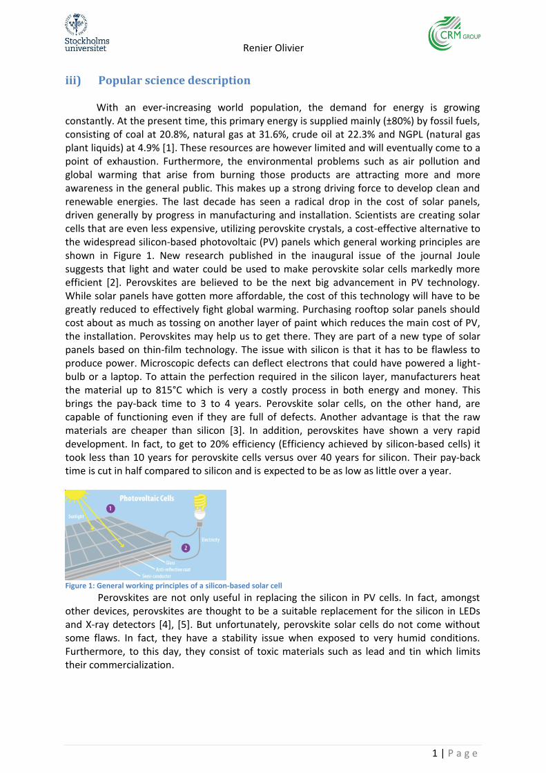
With an ever-increasing world population, the demand for energy is growing constantly. At the present time, this primary energy is supplied mainly (±80%) by fossil fuels, consisting of coal at 20.8%, natural gas at 31.6%, crude oil at 22.3% and NGPL (natural gas plant liquids) at 4.9% [1]. These resources are however limited and will eventually come to a point of exhaustion. Furthermore, the environmental problems such as air pollution and global warming that arise from burning those products are attracting more and more awareness in the general public. This makes up a strong driving force to develop clean and renewable energies. The last decade has seen a radical drop in the cost of solar panels, driven generally by progress in manufacturing and installation. Scientists are creating solar cells that are even less expensive, utilizing perovskite crystals, a cost-effective alternative to the widespread silicon-based photovoltaic (PV) panels which general working principles are shown in Figure 1. New research published in the inaugural issue of the journal Joule suggests that light and water could be used to make perovskite solar cells markedly more efficient [2]. Perovskites are believed to be the next big advancement in PV technology. While solar panels have gotten more affordable, the cost of this technology will have to be greatly reduced to effectively fight global warming. Purchasing rooftop solar panels should cost about as much as tossing on another layer of paint which reduces the main cost of PV, the installation. Perovskites may help us to get there. They are part of a new type of solar panels based on thin-film technology. The issue with silicon is that it has to be flawless to produce power. Microscopic defects can deflect electrons that could have powered a light-bulb or a laptop. To attain the perfection required in the silicon layer, manufacturers heat the material up to 815°C which is very a costly process in both energy and money. This brings the pay-back time to 3 to 4 years. Perovskite solar cells, on the other hand, are capable of functioning even if they are full of defects. Another advantage is that the raw materials are cheaper than silicon [3]. In addition, perovskites have shown a very rapid development. In fact, to get to 20% efficiency (Efficiency achieved by silicon-based cells) it took less than 10 years for perovskite cells versus over 40 years for silicon. Their pay-back time is cut in half compared to silicon and is expected to be as low as little over a year.
Figure 1: General working principles of a silicon-based solar cell
Perovskites are not only useful in replacing the silicon in PV cells. In fact, amongst other devices, perovskites are thought to be a suitable replacement for the silicon in LEDs and X-ray detectors [4], [5]. But unfortunately, perovskite solar cells do not come without some flaws. In fact, they have a stability issue when exposed to very humid conditions. Furthermore, to this day, they consist of toxic materials such as lead and tin which limits their commercialization.
Renier Olivier
2 | P a g e
iv) Abstract
Perovskites-photovoltaic cells are a type of photovoltaic cells which include a chemical compound having perovskite structure, most often a hybrid organic-inorganic lead or a tin halide, in its light-converting active layer. The efficiency of photovoltaic cells used in these materials is increasing constantly since the beginning of the new millennium. It went from 3.8% in 2009 [6] to 22.1% [7] in early 2016 [8].Up until today, this is the fastest development in the history of the photovoltaic history. To this day, some stability problems unfortunately still remain unsolved. However, this technology still exhibits a significant margin to improve performance and low production costs. This means that perovskite cells have become commercially attractive, and start-up companies already announce modules on the market by 2019.
This study concluded that the addition of halogenated bidentate additives such as 1,8 Diiodooctane (DIO) not only influenced the performances of perovskite solar cells but also their stability over time. By fine elemental analysis, it was concluded that the addition of chlorine in the solution did not imply the substitution of iodide by chlorine in the structure. Chlorine is therefore believed to play a role in getting rid of the excess of methylamine, thus helping stabilizing the cell and enhancing its performance. As requested by the industry, this work demonstrated the feasibility of replacing the electron transport layer (ETL) of TiO2 by a materials obtained by liquid low-temperature process (<150°C).
v) Introduction to the company
The CRM (Centre de Recherche Métalurgique: Metallurgical research center) was created in 1948 by the Belgian steel industry. Their goal is to offer R&D and technology solutions focusing on the development of innovative processes and products that create value for our industrial partners. AC&CS (Advanced Coatings & Construction Solutions) was created in 1990 as a local R&D center for the industry located in Cockerill-Sambre. They are implanted on the campus of Liège’s university (ULiège). The research center was formerly under the direction of the ArcelorMittal group before becoming independent at the beginning of the steel crisis in Belgium. They later (2011) fused with the CRM to create the CRM group. While the CRM focuses mainly on the large-scale application and the R&D related to metals, AC&CS has more varied areas of research that encompass paints, coatings, photovoltaic applications, etc. Since then, ArcelorMittal still remained their biggest client and influence on the researched topics.
Renier Olivier
3 | P a g e
Introduction
1.1 General introduction
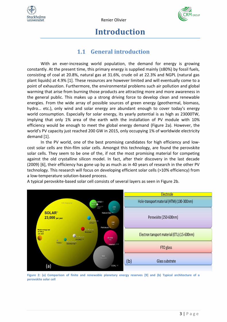
With an ever-increasing world population, the demand for energy is growing constantly. At the present time, this primary energy is supplied mainly (±80%) by fossil fuels, consisting of coal at 20.8%, natural gas at 31.6%, crude oil at 22.3% and NGPL (natural gas plant liquids) at 4.9% [1]. These resources are however limited and will eventually come to a point of exhaustion. Furthermore, the environmental problems such air pollution and global warming that arise from burning those products are attracting more and more awareness in the general public. This makes up a strong driving force to develop clean and renewable energies. From the wide array of possible sources of green energy (geothermal, biomass, hydro… etc.), only wind and solar energy are abundant enough to cover today’s energy world consumption. Especially for solar energy, its yearly potential is as high as 23000TW, implying that only 1% area of the earth with the installation of PV module with 10% efficiency would be enough to meet the global energy demand (Figure 2a). However, the world’s PV capacity just reached 200 GW in 2015, only occupying 1% of worldwide electricity demand [1].
In the PV world, one of the best promising candidates for high efficiency and low-cost solar cells are thin-film solar cells. Amongst this technology, are found the perovskite solar cells. They seem to be one of the, if not the most promising material for competing against the old crystalline silicon model. In fact, after their discovery in the last decade (2009) [6], their efficiency has gone up by as much as in 40 years of research in the other PV technology. This research will focus on developing efficient solar cells (>10% efficiency) from a low-temperature solution-based process. A typical perovskite-based solar cell consists of several layers as seen in Figure 2b.
Figure 2: (a) Comparison of finite and renewable planetary energy reserves [9] and (b) Typical architecture of a perovskite solar cell
Renier Olivier
4 | P a g e
1.2 Introduction to the system studied
1.2.1 Solar cells
Photovoltaic solar cells rely on the principle of transforming the energy contained in
the rays of the sun into electrical energy. This technology proves to become more and more important for the future of our planet as it is renewable and technically infinite. Once this technology reaches its full potential, it could potentially replace the current classical and environment-harming ways of production. As of now, the photovoltaic technology can be divided into two main groups (Figure 3a).
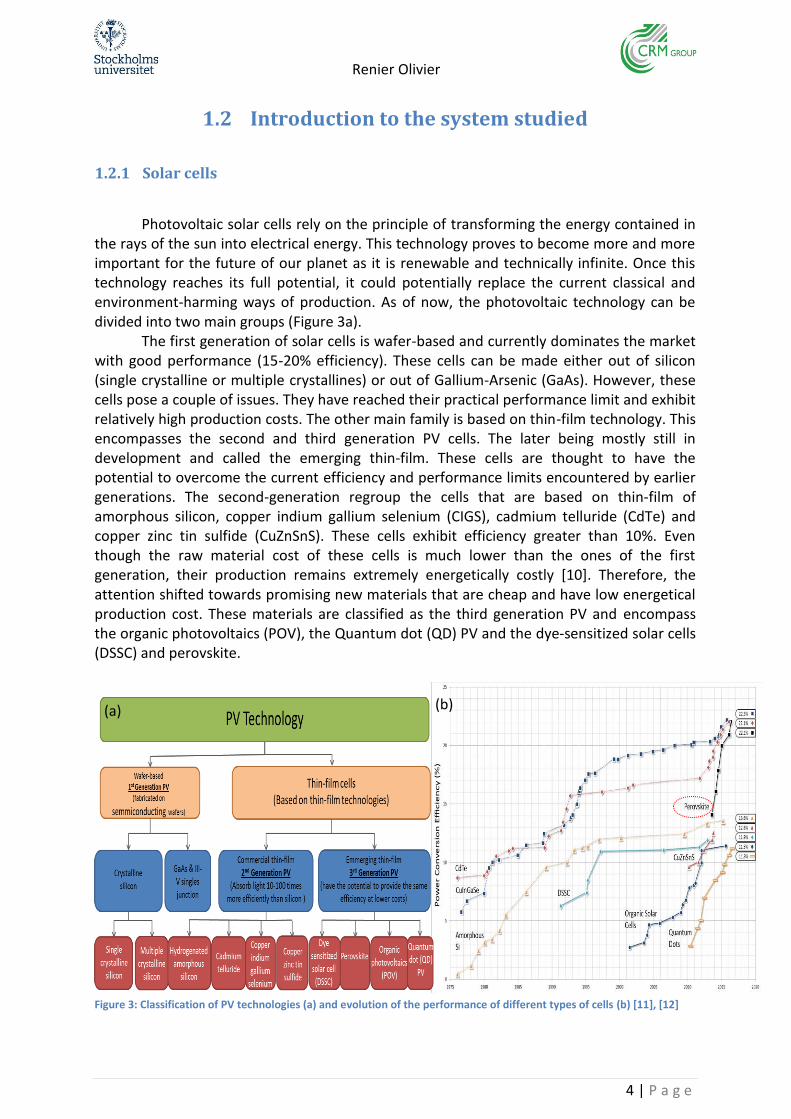
The first generation of solar cells is wafer-based and currently dominates the market with good performance (15-20% efficiency). These cells can be made either out of silicon (single crystalline or multiple crystallines) or out of Gallium-Arsenic (GaAs). However, these cells pose a couple of issues. They have reached their practical performance limit and exhibit relatively high production costs. The other main family is based on thin-film technology. This encompasses the second and third generation PV cells. The later being mostly still in development and called the emerging thin-film. These cells are thought to have the potential to overcome the current efficiency and performance limits encountered by earlier generations. The second-generation regroup the cells that are based on thin-film of amorphous silicon, copper indium gallium selenium (CIGS), cadmium telluride (CdTe) and copper zinc tin sulfide (CuZnSnS). These cells exhibit efficiency greater than 10%. Even though the raw material cost of these cells is much lower than the ones of the first generation, their production remains extremely energetically costly [10]. Therefore, the attention shifted towards promising new materials that are cheap and have low energetical production cost. These materials are classified as the third generation PV and encompass the organic photovoltaics (POV), the Quantum dot (QD) PV and the dye-sensitized solar cells (DSSC) and perovskite.
Figure 3: Classification of PV technologies (a) and evolution of the performance of different types of cells (b) [11], [12]
(b) (a)
Renier Olivier
5 | P a g e
Perovskite solar cells are associated to DSSC as the difference between these two
relies on the sensitizer used as a light converter. They also attracted a lot of attention due to their very rapid development. In fact, since their first used in the solar cell in 2009, they have reached an efficiency equivalent to the first generation. In contrast, it took over 40 years for the silicon-based technology to reach the same standpoint (Figure 3b). However, this technology still suffers from a few problems [13]. Some of those problems include the use of toxic materials such as lead and expensive materials such as gold for the counter-electrode. Some other issues are encountered with the stability of the perovskite structure. In fact, it is sensitive to moisture and degrades rapidly.
1.2.2 Physical principles
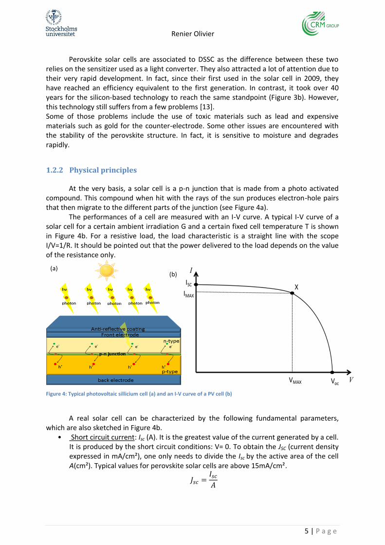
At the very basis, a solar cell is a p-n junction that is made from a photo activated compound. This compound when hit with the rays of the sun produces electron-hole pairs that then migrate to the different parts of the junction (see Figure 4a).
The performances of a cell are measured with an I-V curve. A typical I-V curve of a solar cell for a certain ambient irradiation G and a certain fixed cell temperature T is shown in Figure 4b. For a resistive load, the load characteristic is a straight line with the scope I/V=1/R. It should be pointed out that the power delivered to the load depends on the value of the resistance only.
Figure 4: Typical photovoltaic sillicium cell (a) and an I-V curve of a PV cell (b)
A real solar cell can be characterized by the following fundamental parameters,
which are also sketched in Figure 4b. • Short circuit current: Isc (A). It is the greatest value of the current generated by a cell.
It is produced by the short circuit conditions: V= 0. To obtain the JSC (current density expressed in mA/cm²), one only needs to divide the Isc by the active area of the cell A(cm²). Typical values for perovskite solar cells are above 15mA/cm².
𝐽𝑠𝑐 =𝐼𝑠𝑐
𝐴
Renier Olivier
6 | P a g e
• Open circuit voltage corresponds to the voltage drop (in V) across the diode (p-n junction) when it is traversed by the photocurrent Iph (namely IL= Iph), namely when the generated currents is I= 0. It reflects the voltage of the cell in the night and it can be mathematically expressed as:
𝑉𝑜𝑐 = 𝑛𝑘𝑇
𝑞ln (
𝐼𝐿
𝐼0)
Where I0 is the temperature dependence of the diode saturation current, IL is
the temperature dependence of the photocurrent. n is the diode quality factor and k, T and q are constants that approximate to kT/q= 0.0258V. Commercial solar cells have a value for the VOC exceeding 0.6V
• Maximum power point is the operating point X(Vmax, Imax) in Figure 6, at which the
power dissipated in the resistive load is maximum: Pmax = VmaxImax.
• Maximum efficiency is the ratio between the maximum power and the incident light power.
𝜂 =𝑃𝑚𝑎𝑥
𝑃𝑖𝑛=
𝐼𝑚𝑎𝑥𝑉𝑚𝑎𝑥
𝐴𝐺𝑎
Where Ga is the ambient irradiation and A is the cell area. Typical efficiencies
are as follow: Si-based solar cell ±20%, good Perovskite solar cells >10%
• The Fill factor is the ratio between the maximum power that can be delivered to the load and the product of Isc and VOC:
𝐹𝐹 =𝑃𝑚𝑎𝑥
𝑉𝑜𝑐𝐼𝑠𝑐=
𝐼𝑚𝑎𝑥𝑉𝑚𝑎𝑥
𝑉𝑜𝑐𝐼𝑠𝑐
The fill factor is a measure of the real I-V characteristic. Its value is higher than 70 for good cells. The fill factor diminishes as the cell temperature is increased. The open circuit voltage increases logarithmically with the ambient irradiation, while the short circuit current is a linear function of the ambient irradiation. The dominant effect with increasing cell’s temperature is the linear decrease of the open circuit voltage, the cell being thus less efficient. The short circuit current slightly increases with the cell temperature [14].
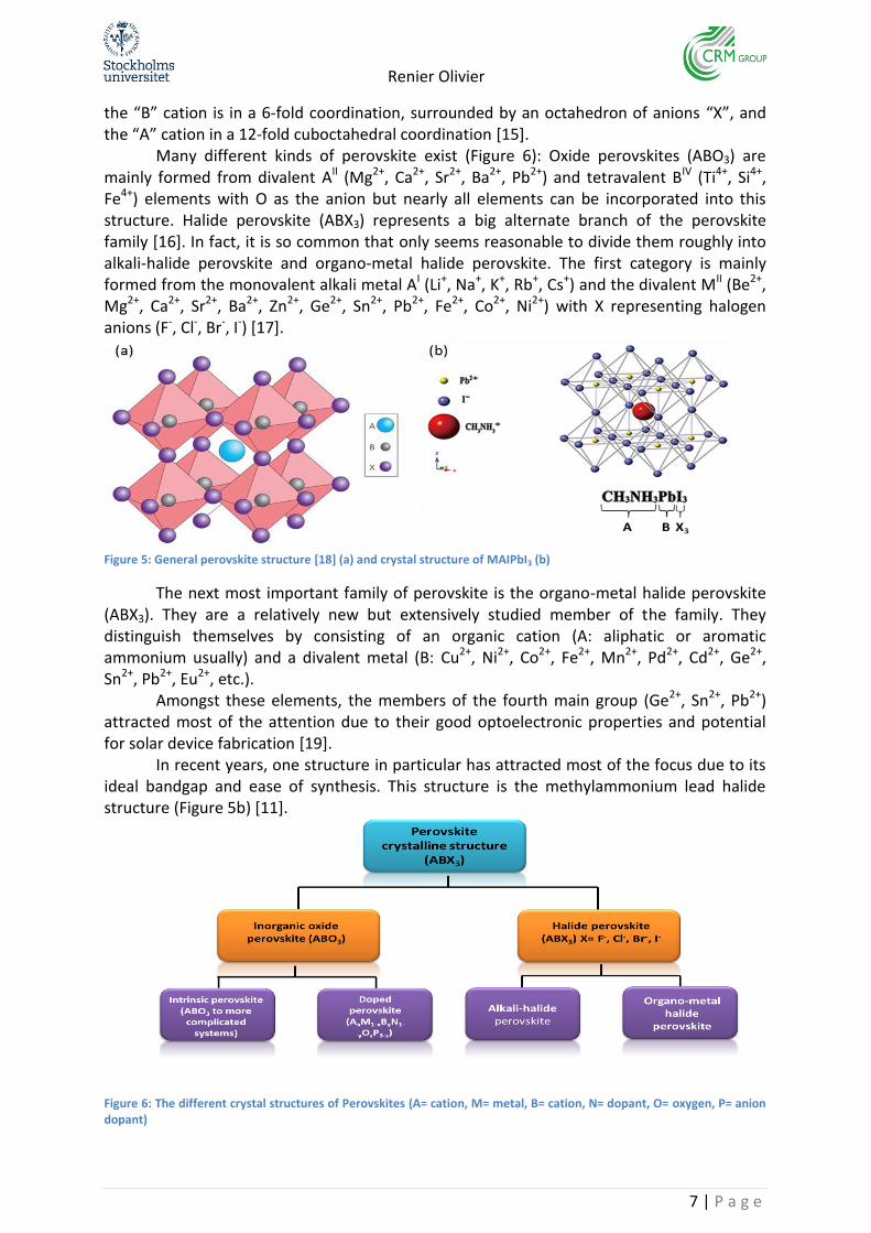
1.2.3 Perovskite
Originally, the term “perovskite” refers to a calcium titanium oxide mineral that was discovered in the Ural Mountains of Russia by Gustav Rose in 1839 and named after the mineralogist L.A. Perovksi. It is defined by the chemical formula of CaTiO3. Since then, a lot of other compounds have been found to exhibit the same crystallographic arrangement and the formula for perovskite has been generalized to ABX3 where “A” and “B” are two cations of very different sizes, and “X” is an anion that bonds to both (Figure 5a). Nowadays, the word perovskite is used to describe any chemical compound that exhibits the same crystal structure as the calcium titanium oxide CaTiO3. The structure can take many different space-groups but the cubic structure is considered as the standard structure. In this configuration,
Renier Olivier
7 | P a g e
the “B” cation is in a 6-fold coordination, surrounded by an octahedron of anions “X”, and the “A” cation in a 12-fold cuboctahedral coordination [15].
Many different kinds of perovskite exist (Figure 6): Oxide perovskites (ABO3) are mainly formed from divalent AII (Mg2+, Ca2+, Sr2+, Ba2+, Pb2+) and tetravalent BIV (Ti4+, Si4+, Fe4+) elements with O as the anion but nearly all elements can be incorporated into this structure. Halide perovskite (ABX3) represents a big alternate branch of the perovskite family [16]. In fact, it is so common that only seems reasonable to divide them roughly into alkali-halide perovskite and organo-metal halide perovskite. The first category is mainly formed from the monovalent alkali metal AI (Li+, Na+, K+, Rb+, Cs+) and the divalent MII (Be2+, Mg2+, Ca2+, Sr2+, Ba2+, Zn2+, Ge2+, Sn2+, Pb2+, Fe2+, Co2+, Ni2+) with X representing halogen anions (F-, Cl-, Br-, I-) [17].
Figure 5: General perovskite structure [18] (a) and crystal structure of MAIPbI3 (b)
The next most important family of perovskite is the organo-metal halide perovskite (ABX3). They are a relatively new but extensively studied member of the family. They distinguish themselves by consisting of an organic cation (A: aliphatic or aromatic ammonium usually) and a divalent metal (B: Cu2+, Ni2+, Co2+, Fe2+, Mn2+, Pd2+, Cd2+, Ge2+, Sn2+, Pb2+, Eu2+, etc.).
Amongst these elements, the members of the fourth main group (Ge2+, Sn2+, Pb2+) attracted most of the attention due to their good optoelectronic properties and potential for solar device fabrication [19].
In recent years, one structure in particular has attracted most of the focus due to its ideal bandgap and ease of synthesis. This structure is the methylammonium lead halide structure (Figure 5b) [11].
Figure 6: The different crystal structures of Perovskites (A= cation, M= metal, B= cation, N= dopant, O= oxygen, P= anion dopant)
Renier Olivier
8 | P a g e
It was only in 1957 that Christian Møller discovered that Alkali-halide perovskite behaved as semiconductors [20]. Since then, multiple structures with the basic formula CH3NH3PbX3 (where X= I, F, Cl Br) have been studied but their application into thin-film for photovoltaic application only started at the end of the 2000s.
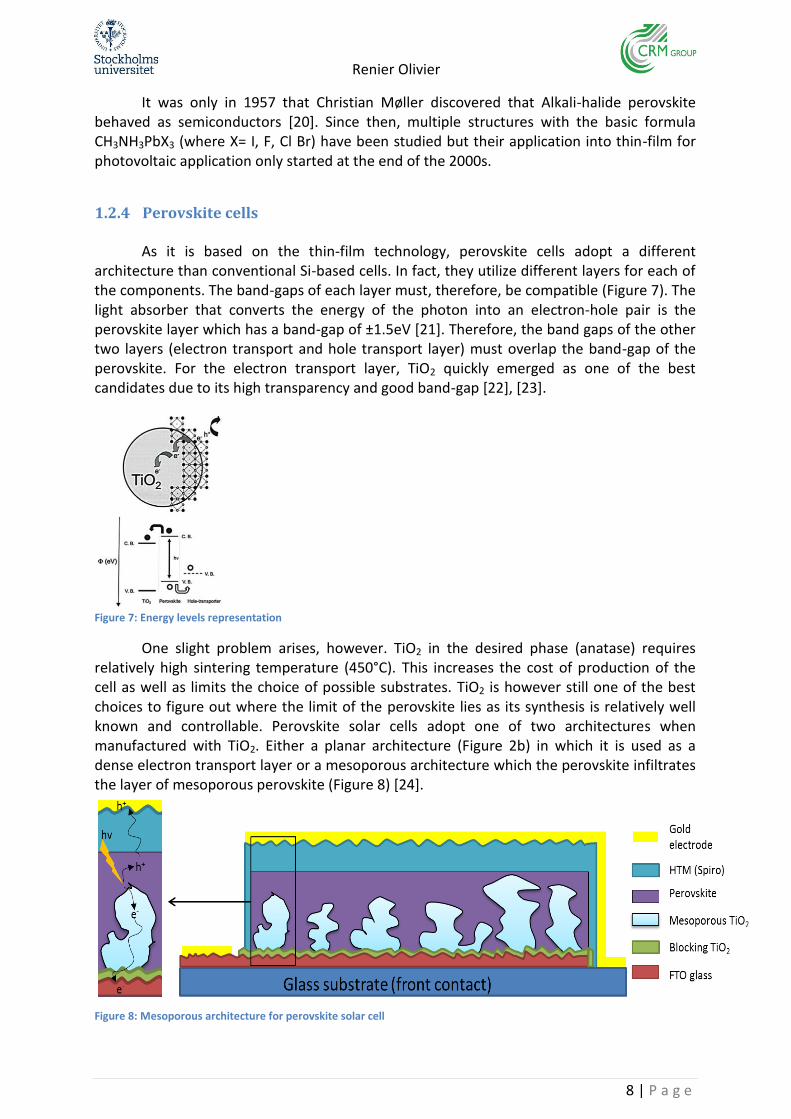
1.2.4 Perovskite cells
As it is based on the thin-film technology, perovskite cells adopt a different architecture than conventional Si-based cells. In fact, they utilize different layers for each of the components. The band-gaps of each layer must, therefore, be compatible (Figure 7). The light absorber that converts the energy of the photon into an electron-hole pair is the perovskite layer which has a band-gap of ±1.5eV [21]. Therefore, the band gaps of the other two layers (electron transport and hole transport layer) must overlap the band-gap of the perovskite. For the electron transport layer, TiO2 quickly emerged as one of the best candidates due to its high transparency and good band-gap [22], [23].
Figure 7: Energy levels representation
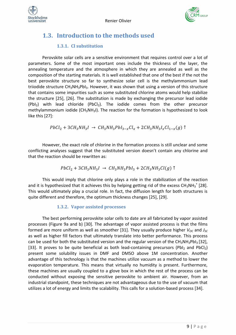
One slight problem arises, however. TiO2 in the desired phase (anatase) requires relatively high sintering temperature (450°C). This increases the cost of production of the cell as well as limits the choice of possible substrates. TiO2 is however still one of the best choices to figure out where the limit of the perovskite lies as its synthesis is relatively well known and controllable. Perovskite solar cells adopt one of two architectures when manufactured with TiO2. Either a planar architecture (Figure 2b) in which it is used as a dense electron transport layer or a mesoporous architecture which the perovskite infiltrates the layer of mesoporous perovskite (Figure 8) [24].
Figure 8: Mesoporous architecture for perovskite solar cell
Renier Olivier
9 | P a g e
1.3. Introduction to the methods used
1.3.1. Cl substitution
Perovskite solar cells are a sensitive environment that requires control over a lot of parameters. Some of the most important ones include the thickness of the layer, the annealing temperature and the atmosphere in which they are annealed as well as the composition of the starting materials. It is well established that one of the best if the not the best perovskite structure so far to synthesize solar cell is the methylammonium lead triiodide structure CH3NH3PbI3. However, it was shown that using a version of this structure that contains some impurities such as some substituted chlorine atoms would help stabilize the structure [25], [26]. The substitution is made by exchanging the precursor lead iodide (PbI2) with lead chloride (PbCl2). The iodide comes from the other precursor methylammonium iodide (CH3NH3I). The reaction for the formation is hypothesized to look like this [27]:
𝑃𝑏𝐶𝑙2 + 3𝐶𝐻3𝑁𝐻3𝐼 → 𝐶𝐻3𝑁𝐻3𝑃𝑏𝐼3−𝑥𝐶𝑙𝑥 + 2𝐶𝐻3𝑁𝐻3𝐼𝑥𝐶𝑙1−𝑥(𝑔) ↑
However, the exact role of chlorine in the formation process is still unclear and some conflicting analyses suggest that the substituted version doesn’t contain any chlorine and that the reaction should be rewritten as:
𝑃𝑏𝐶𝑙2 + 3𝐶𝐻3𝑁𝐻3𝐼 → 𝐶𝐻3𝑁𝐻3𝑃𝑏𝐼3 + 2𝐶𝐻3𝑁𝐻3𝐶𝑙(𝑔) ↑
This would imply that chlorine only plays a role in the stabilization of the reaction and it is hypothesized that it achieves this by helping getting rid of the excess CH3NH3
+ [28]. This would ultimately play a crucial role. In fact, the diffusion length for both structures is quite different and therefore, the optimum thickness changes [25], [29].
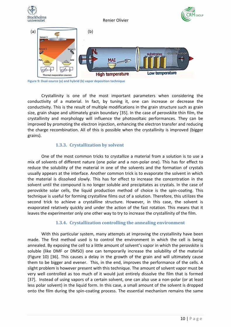
1.3.2. Vapor assisted processes
The best performing perovskite solar cells to date are all fabricated by vapor assisted processes (Figure 9a and b) [30]. The advantage of vapor assisted process is that the films formed are more uniform as well as smoother [31]. They usually produce higher VOC and JSC as well as higher fill factors that ultimately translate into better performance. This process can be used for both the substituted version and the regular version of the CH3NH3PbI3 [32], [33]. It proves to be quite beneficial as both lead-containing precursors (PbI2 and PbCl2) present some solubility issues in DMF and DMSO above 1M concentration. Another advantage of this technology is that the machines utilize vacuum as a method to lower the evaporation temperature. This means that virtually no humidity is present. Furthermore, these machines are usually coupled to a glove box in which the rest of the process can be conducted without exposing the sensitive perovskite to ambient air. However, from an industrial standpoint, these techniques are not advantageous due to the use of vacuum that utilizes a lot of energy and limits the scalability. This calls for a solution-based process [34].
Renier Olivier
10 | P a g e
Figure 9: Dual-source (a) and hybrid (b) vapor deposition technique
Crystallinity is one of the most important parameters when considering the
conductivity of a material. In fact, by tuning it, one can increase or decrease the conductivity. This is the result of multiple modifications in the grain structure such as grain size, grain shape and ultimately grain boundary [35]. In the case of perovskite thin film, the crystallinity and morphology will influence the photovoltaic performances. They can be improved by promoting the electron injection, enhancing the electron transfer and reducing the charge recombination. All of this is possible when the crystallinity is improved (bigger grains).
1.3.3. Crystallization by solvent
One of the most common tricks to crystallize a material from a solution is to use a mix of solvents of different nature (one polar and a non-polar one). This has for effect to reduce the solubility of the material in one of the solvents and the formation of crystals usually appears at the interface. Another common trick is to evaporate the solvent in which the material is dissolved slowly. This has for effect to increase the concentration in the solvent until the compound is no longer soluble and precipitates as crystals. In the case of perovskite solar cells, the liquid production method of choice is the spin-coating. This technique is useful for forming crystalline films out of a solution. Therefore, this utilizes the second trick to achieve a crystalline structure. However, in this case, the solvent is evaporated relatively quickly and under the action of the fast rotation. This means that it leaves the experimenter only one other way to try to increase the crystallinity of the film.
1.3.4. Crystallization controlling the annealing environment
With this particular system, many attempts at improving the crystallinity have been made. The first method used is to control the environment in which the cell is being annealed. By exposing the cell to a little amount of solvent’s vapor in which the perovskite is soluble (like DMF or DMSO) one can temporarily increase the solubility of the material (Figure 10) [36]. This causes a delay in the growth of the grain and will ultimately cause them to be bigger and evener. This, in the end, improves the performance of the cells. A slight problem is however present with this technique. The amount of solvent vapor must be very well controlled as too much of it would just entirely dissolve the film that is formed [37]. Instead of using vapors of a certain solvent, one can also use a non-polar (or at least less polar solvent) in the liquid form. In this case, a small amount of the solvent is dropped onto the film during the spin-coating process. The essential mechanism remains the same
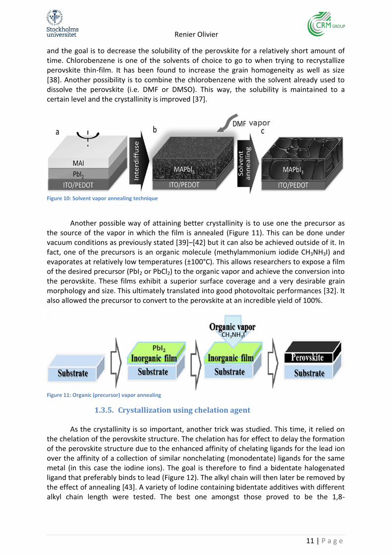
Renier Olivier
11 | P a g e
and the goal is to decrease the solubility of the perovskite for a relatively short amount of time. Chlorobenzene is one of the solvents of choice to go to when trying to recrystallize perovskite thin-film. It has been found to increase the grain homogeneity as well as size [38]. Another possibility is to combine the chlorobenzene with the solvent already used to dissolve the perovskite (i.e. DMF or DMSO). This way, the solubility is maintained to a certain level and the crystallinity is improved [37].
Figure 10: Solvent vapor annealing technique
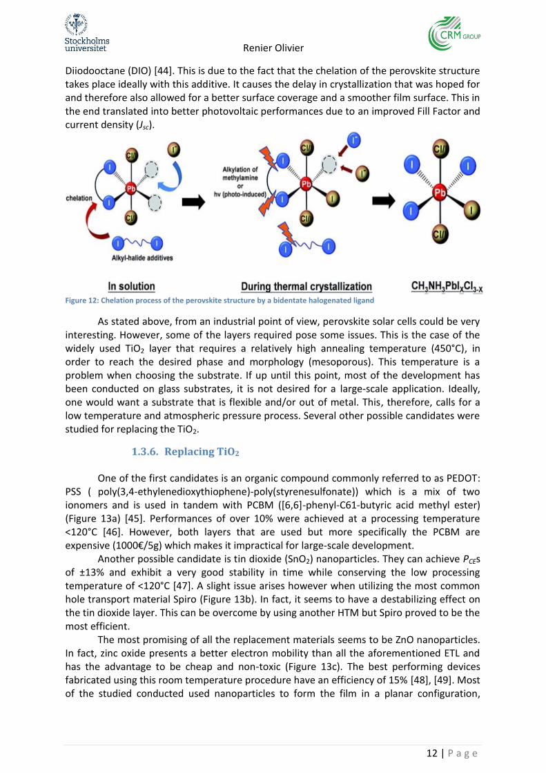
Another possible way of attaining better crystallinity is to use one the precursor as
the source of the vapor in which the film is annealed (Figure 11). This can be done under vacuum conditions as previously stated [39]–[42] but it can also be achieved outside of it. In fact, one of the precursors is an organic molecule (methylammonium iodide CH3NH3I) and evaporates at relatively low temperatures (±100°C). This allows researchers to expose a film of the desired precursor (PbI2 or PbCl2) to the organic vapor and achieve the conversion into the perovskite. These films exhibit a superior surface coverage and a very desirable grain morphology and size. This ultimately translated into good photovoltaic performances [32]. It also allowed the precursor to convert to the perovskite at an incredible yield of 100%.
Figure 11: Organic (precursor) vapor annealing
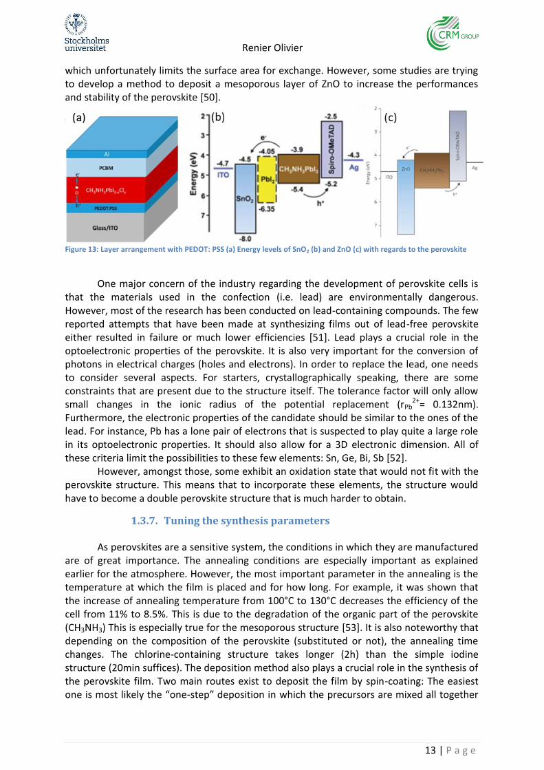
1.3.5. Crystallization using chelation agent
As the crystallinity is so important, another trick was studied. This time, it relied on the chelation of the perovskite structure. The chelation has for effect to delay the formation of the perovskite structure due to the enhanced affinity of chelating ligands for the lead ion over the affinity of a collection of similar nonchelating (monodentate) ligands for the same metal (in this case the iodine ions). The goal is therefore to find a bidentate halogenated ligand that preferably binds to lead (Figure 12). The alkyl chain will then later be removed by the effect of annealing [43]. A variety of Iodine containing bidentate additives with different alkyl chain length were tested. The best one amongst those proved to be the 1,8-
Renier Olivier
12 | P a g e
Diiodooctane (DIO) [44]. This is due to the fact that the chelation of the perovskite structure takes place ideally with this additive. It causes the delay in crystallization that was hoped for and therefore also allowed for a better surface coverage and a smoother film surface. This in the end translated into better photovoltaic performances due to an improved Fill Factor and current density (Jsc).
Figure 12: Chelation process of the perovskite structure by a bidentate halogenated ligand
As stated above, from an industrial point of view, perovskite solar cells could be very interesting. However, some of the layers required pose some issues. This is the case of the widely used TiO2 layer that requires a relatively high annealing temperature (450°C), in order to reach the desired phase and morphology (mesoporous). This temperature is a problem when choosing the substrate. If up until this point, most of the development has been conducted on glass substrates, it is not desired for a large-scale application. Ideally, one would want a substrate that is flexible and/or out of metal. This, therefore, calls for a low temperature and atmospheric pressure process. Several other possible candidates were studied for replacing the TiO2.
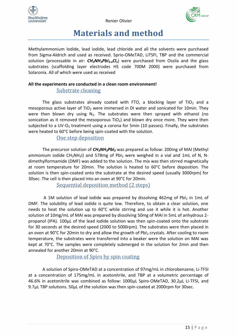
1.3.6. Replacing TiO2 One of the first candidates is an organic compound commonly referred to as PEDOT:
PSS ( poly(3,4-ethylenedioxythiophene)-poly(styrenesulfonate)) which is a mix of two ionomers and is used in tandem with PCBM ([6,6]-phenyl-C61-butyric acid methyl ester) (Figure 13a) [45]. Performances of over 10% were achieved at a processing temperature <120°C [46]. However, both layers that are used but more specifically the PCBM are expensive (1000€/5g) which makes it impractical for large-scale development.
Another possible candidate is tin dioxide (SnO2) nanoparticles. They can achieve PCEs of ±13% and exhibit a very good stability in time while conserving the low processing temperature of <120°C [47]. A slight issue arises however when utilizing the most common hole transport material Spiro (Figure 13b). In fact, it seems to have a destabilizing effect on the tin dioxide layer. This can be overcome by using another HTM but Spiro proved to be the most efficient.
The most promising of all the replacement materials seems to be ZnO nanoparticles. In fact, zinc oxide presents a better electron mobility than all the aforementioned ETL and has the advantage to be cheap and non-toxic (Figure 13c). The best performing devices fabricated using this room temperature procedure have an efficiency of 15% [48], [49]. Most of the studied conducted used nanoparticles to form the film in a planar configuration,
Renier Olivier
13 | P a g e
which unfortunately limits the surface area for exchange. However, some studies are trying to develop a method to deposit a mesoporous layer of ZnO to increase the performances and stability of the perovskite [50].
Figure 13: Layer arrangement with PEDOT: PSS (a) Energy levels of SnO2 (b) and ZnO (c) with regards to the perovskite
One major concern of the industry regarding the development of perovskite cells is
that the materials used in the confection (i.e. lead) are environmentally dangerous. However, most of the research has been conducted on lead-containing compounds. The few reported attempts that have been made at synthesizing films out of lead-free perovskite either resulted in failure or much lower efficiencies [51]. Lead plays a crucial role in the optoelectronic properties of the perovskite. It is also very important for the conversion of photons in electrical charges (holes and electrons). In order to replace the lead, one needs to consider several aspects. For starters, crystallographically speaking, there are some constraints that are present due to the structure itself. The tolerance factor will only allow small changes in the ionic radius of the potential replacement (rPb
2+= 0.132nm). Furthermore, the electronic properties of the candidate should be similar to the ones of the lead. For instance, Pb has a lone pair of electrons that is suspected to play quite a large role in its optoelectronic properties. It should also allow for a 3D electronic dimension. All of these criteria limit the possibilities to these few elements: Sn, Ge, Bi, Sb [52].
However, amongst those, some exhibit an oxidation state that would not fit with the perovskite structure. This means that to incorporate these elements, the structure would have to become a double perovskite structure that is much harder to obtain.
1.3.7. Tuning the synthesis parameters As perovskites are a sensitive system, the conditions in which they are manufactured are of great importance. The annealing conditions are especially important as explained earlier for the atmosphere. However, the most important parameter in the annealing is the temperature at which the film is placed and for how long. For example, it was shown that the increase of annealing temperature from 100°C to 130°C decreases the efficiency of the cell from 11% to 8.5%. This is due to the degradation of the organic part of the perovskite (CH3NH3) This is especially true for the mesoporous structure [53]. It is also noteworthy that depending on the composition of the perovskite (substituted or not), the annealing time changes. The chlorine-containing structure takes longer (2h) than the simple iodine structure (20min suffices). The deposition method also plays a crucial role in the synthesis of the perovskite film. Two main routes exist to deposit the film by spin-coating: The easiest one is most likely the “one-step” deposition in which the precursors are mixed all together

Renier Olivier
14 | P a g e
and dissolved in the appropriate solvent before being deposited [54]. Another possibility is to deposit one of the precursor alone (usually the lead-containing one) and annealing this film first before dipping it into a solution of the other precursor [55]. This method is called the sequential deposition method or “two-steps”. This influences the performances slightly but also allows to modify the annealing time (two-steps deposition requires less annealing time) [56]. Stability is the main issue in perovskite. Many studies show the stability of their cell by measuring the efficiencies over a certain period of time. However, very few followed the evolution of the composition of the perovskite. Raman spectroscopy allows researchers to detect the changes in the lead-iodide (Pb-I) bond that is suspected to be the reason for the loss of efficiency [57]–[60]. The objectives of this work were to develop more efficient cells than available in the company (>10% PCE) and to see if a viable replacement for the TiO2 that could be applied at low temperature (<150°C) could be found.
Renier Olivier
15 | P a g e
Materials and method
Methylammonium Iodide, lead iodide, lead chloride and all the solvents were purchased from Sigma-Aldrich and used as received. Sprio-OMeTAD, LiTSFI, TBP and the commercial solution (processable in air: CH3NH3PbI3-xClx) were purchased from Ossila and the glass substrates (scaffolding layer electrodes HS code 700M 2000) were purchased from Solaronix. All of which were used as received All the experiments are conducted in a clean room environment!
Substrate cleaning
The glass substrates already coated with FTO, a blocking layer of TiO2 and a mesoporous active layer of TiO2 were immersed in DI water and sonicated for 10min. They were then blown dry using N2. The substrates were then sprayed with ethanol (no sonication as it removed the mesoporous TiO2) and blown dry once more. They were then subjected to a UV-O3 treatment using a corona for 5min (10 passes). Finally, the substrates were heated to 60°C before being spin-coated with the solution.
One step deposition
The precursor solution of CH3NH3PbI3 was prepared as follow: 200mg of MAI (Methyl ammonium iodide CH3NH3I) and 578mg of PbI2 were weighed in a vial and 1mL of N, N-dimethylformamide (DMF) was added to the solution. The mix was then stirred magnetically at room temperature for 20min. The solution is heated to 60°C before deposition. The solution is then spin-coated onto the substrate at the desired speed (usually 3000rpm) for 30sec. The cell is then placed into an oven at 90°C for 20min.
Sequential deposition method (2 steps)
A 1M solution of lead iodide was prepared by dissolving 462mg of PbI2 in 1mL of DMF. The solubility of lead iodide is quite low. Therefore, to obtain a clear solution, one needs to heat the solution up to 60°C while stirring and use it while it is hot. Another solution of 10mg/mL of MAI was prepared by dissolving 50mg of MAI in 5mL of anhydrous 2-propanol (IPA). 100µL of the lead iodide solution was then spin-coated onto the substrate for 30 seconds at the desired speed (2000 to 5000rpm). The substrates were then placed in an oven at 90°C for 20min to dry and allow the growth of PbI2 crystals. After cooling to room temperature, the substrates were transferred into a beaker were the solution on MAI was kept at 70°C. The samples were completely submerged in the solution for 2min and then annealed for another 20min at 90°C.
Deposition of Spiro by spin coating
A solution of Spiro-OMeTAD at a concentration of 97mg/mL in chlorobenzene, Li-TFSI at a concentration of 175mg/mL in acetonitrile, and TBP at a volumetric percentage of 46.6% in acetonitrile was combined as follow: 1000μL Spiro-OMeTAD, 30.2μL Li-TFSI, and 9.7μL TBP solutions. 50µL of the solution was then spin-coated at 2000rpm for 30sec.
Renier Olivier
16 | P a g e
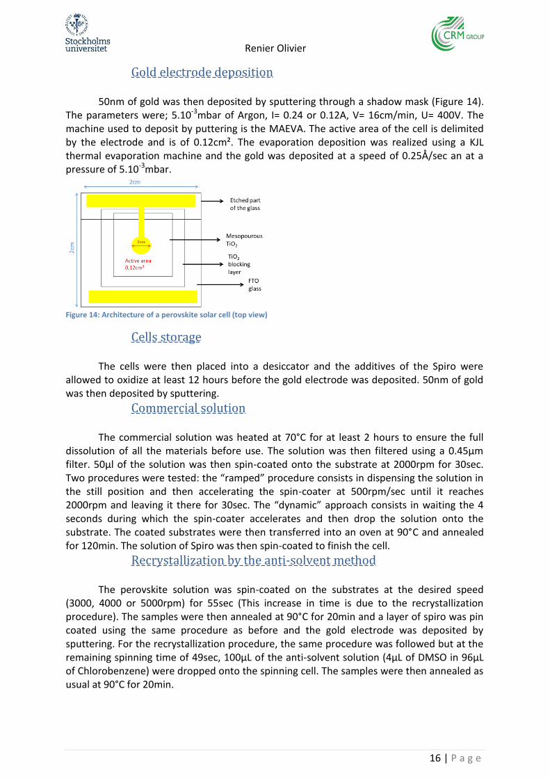
Gold electrode deposition
50nm of gold was then deposited by sputtering through a shadow mask (Figure 14). The parameters were; 5.10-3mbar of Argon, I= 0.24 or 0.12A, V= 16cm/min, U= 400V. The machine used to deposit by puttering is the MAEVA. The active area of the cell is delimited by the electrode and is of 0.12cm². The evaporation deposition was realized using a KJL thermal evaporation machine and the gold was deposited at a speed of 0.25Å/sec an at a pressure of 5.10-3mbar.
Figure 14: Architecture of a perovskite solar cell (top view)
Cells storage
The cells were then placed into a desiccator and the additives of the Spiro were allowed to oxidize at least 12 hours before the gold electrode was deposited. 50nm of gold was then deposited by sputtering.
Commercial solution
The commercial solution was heated at 70°C for at least 2 hours to ensure the full dissolution of all the materials before use. The solution was then filtered using a 0.45µm filter. 50µl of the solution was then spin-coated onto the substrate at 2000rpm for 30sec. Two procedures were tested: the “ramped” procedure consists in dispensing the solution in the still position and then accelerating the spin-coater at 500rpm/sec until it reaches 2000rpm and leaving it there for 30sec. The “dynamic” approach consists in waiting the 4 seconds during which the spin-coater accelerates and then drop the solution onto the substrate. The coated substrates were then transferred into an oven at 90°C and annealed for 120min. The solution of Spiro was then spin-coated to finish the cell.
Recrystallization by the anti-solvent method
The perovskite solution was spin-coated on the substrates at the desired speed (3000, 4000 or 5000rpm) for 55sec (This increase in time is due to the recrystallization procedure). The samples were then annealed at 90°C for 20min and a layer of spiro was pin coated using the same procedure as before and the gold electrode was deposited by sputtering. For the recrystallization procedure, the same procedure was followed but at the remaining spinning time of 49sec, 100µL of the anti-solvent solution (4µL of DMSO in 96µL of Chlorobenzene) were dropped onto the spinning cell. The samples were then annealed as usual at 90°C for 20min.
Renier Olivier
17 | P a g e
Recrystallization procedure by solvent annealing The perovskite solution is deposited by spin-coating at the desired speed for 30sec. the cell is then transferred to a hot plate set at 100°C and covered with a petri-dish. 10µL of solvent is then deposited at the edge of the petri-dish and the substrate is annealed for 2h.
As seen in the literature, the substituted version of CH3NH3PbI3 with chlorine (CH3NH3PbI3-xClx) seems to be more stable in air. Therefore, it was decided to change to this structure for any further experiments.
One step deposition of the substituted structure
Methyl ammonium iodide (209.8mg) and lead chloride (125.8mg) were mixed in the molar ratio 3:1 and dissolved in DMF. The solution was stirred at 70°C for at least 2 hours before use to ensure the complete dissolution of all the reagents. Both the substrates and the solutions were then kept at 60°C. 100µL of the solution was then deposited onto the substrate (dynamically) using a spin-coater at the desired speed for 30sec. The substrates were then annealed at 100°C for 2h. After that, the substrates were allowed to cool down and a solution of doped Spiro-OMeTAD was spin coated at 2000rpm for 30sec. The gold counter electrode was then deposited through a shadow mask using sputtering.
DIO Solution
The precursor solution is prepared in the same way as before dissolving methyl ammonium iodide and lead chloride in the molar ratio 3:1. The desired amount of DIO is then added in wt% (with regards to the perovskite).
A modified version of the substituted one-step procedure
MAI, PbCl2 and lead iodide (PbI2) were mixed in DMF in a molar ratio of 4:1:1. The rest of the procedure remained identical.
Solid state synthesis
MAI and PbCl2 were weighed in a 3:1 molar ratio and mixed together in their powdered form using a mortar and pestle until the characteristic brown color of the perovskite could be observed. The obtained powder was then dissolved in DMF.
Quantum dots (QD)
The solution of commercial quantum dots was spin coated at 1000rpm for 30sec below or above the perovskite layer. It was allowed 5 min at room temperature to dry. The rest of the procedure remained the same as before.
Synthesis of ZnO nanoparticles
The nanoparticles were synthesized according to literature procedures as follows: Zinc acetate dihydrate (2.95g, 13.4mmol) was dissolved in methanol (125 mL) with stirring at 65°C. A solution of KOH (1.48g, 23mmol) in methanol (65 mL) was then added dropwise at 60–65°C over a period of 15min (4.33mL/min). The reaction mixture was stirred for 2.5h at 60-65°C using a reflux condenser. After cooling to room temperature (overnight), the supernatant was decanted and the precipitate washed twice with methanol (20mL). N-

Renier Olivier
18 | P a g e
butanol (70ml), methanol (5mL) and chloroform (5mL) were added to disperse the precipitate and produce a ZnO nanoparticle solution with a concentration of 6mg/ml. Before use, the ZnO nanoparticle solution was filtered through a 0.45µm PVDF syringe filter. The solution was then dispensed onto FTO glass (±140µL) and spin-coated at 3000rpm for 30sec. this procedure was then repeated 3 times to obtain a thickness of 25nm+/-5.
Thickness measurement
The two sides of the substrate (left and right) were cleaned using precision swabs dipped in Chlorobenzene. A Dektak was then used to determine the thickness (physical measurement).
UV-vis spectroscopy The UV-vis measurements were conducted using a Perkin Elmer Lambda 950 recording between 400 and 800nm as this is the visible spectrum of the light.
XRD measurement
The X-ray diffraction experiments were conducted on a Diffractometer D8 from Bruker using a Mo source, in the 2θ configuration. The grazing incidence XRD was recorded on a Bruker D8 using a Cu-source, in the grazing incidence configuration.
Solar simulator The solar simulator measurements were realized on a Newport E190. The illumination measured in number of suns lied between 0.8 and 1 and was checked before every measurement session.
Raman study
Raman studies were conducted using a Micro-Raman confocal Renishaw DM 2500M ren (RL/TL) at 532nm at W5% for 10s, 10 accumulations.
Scanning Electron Microscope The microscopy was realized on a SEM ZEISS SIGMA VP equipped with an EDS detector and a FEG.
XPS spectroscopy
Realized on a Physical electronics Quantum 2000 monochromatic X beam Al K(Alpha) Ar ion gun 4kv-1uA
DLS measurements Dynamic Light Scattering measurements were realized using a Microtrac NANO-flex 180° DLS size.
Renier Olivier
19 | P a g e
Results and discussion
The efficiency of the cell (PCE) is calculated using the following equation:
𝑃𝐶𝐸 =𝑉𝑜𝑐 ∗ 𝐽𝑠𝑐 ∗ 𝐹𝐹
𝑁𝑢𝑚𝑏𝑒𝑟 𝑜𝑓 𝑠𝑢𝑛𝑠
The number of suns is a number determined by the voltage applied to the solar
simulator. It should theoretically always be calibrated for 1. However, it varies quite a lot depending on when the simulator has been turned on and the age of the lamp. Therefore, it is always checked before taking any measurement and plugged into the software. In the case of the simulator used to realize this study, it usually lies between 0.8 and 1sun. Note that the VOC will be expressed at 3 decimal places as it value is comprised between 0 and 1 and that the variations usually occur at the second or third decimal place.
The statistics were obtained by measuring 3 to 5 cells (some cell presented some short-circuits after a few days).
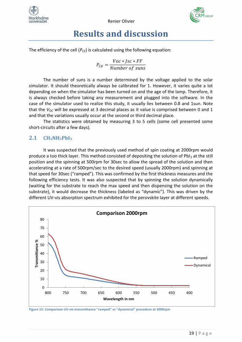
2.1 CH3NH3PbI3
It was suspected that the previously used method of spin coating at 2000rpm would produce a too thick layer. This method consisted of depositing the solution of PbI2 at the still position and the spinning at 500rpm for 30sec to allow the spread of the solution and then accelerating at a rate of 500rpm/sec to the desired speed (usually 2000rpm) and spinning at that speed for 30sec (“ramped”). This was confirmed by the first thickness measures and the following efficiency tests. It was also suspected that by spinning the solution dynamically (waiting for the substrate to reach the max speed and then dispensing the solution on the substrate), it would decrease the thickness (labeled as “dynamic”). This was driven by the different UV-vis absorption spectrum exhibited for the perovskite layer at different speeds.
Figure 15: Comparison UV-vis transmittance "ramped" vs "dynamical" procedure at 2000rpm
0
10
20
30
40
50
60
70
80
800 750 700 650 600 550 500 450 400
Tran
smit
tan
ce %
Wavelength in nm
Comparison 2000rpm
Ramped
Dynamical
Renier Olivier
20 | P a g e
Figure 16: Comparison UV-vis transmittance "ramped" vs "dynamical" procedure at 3000rpm
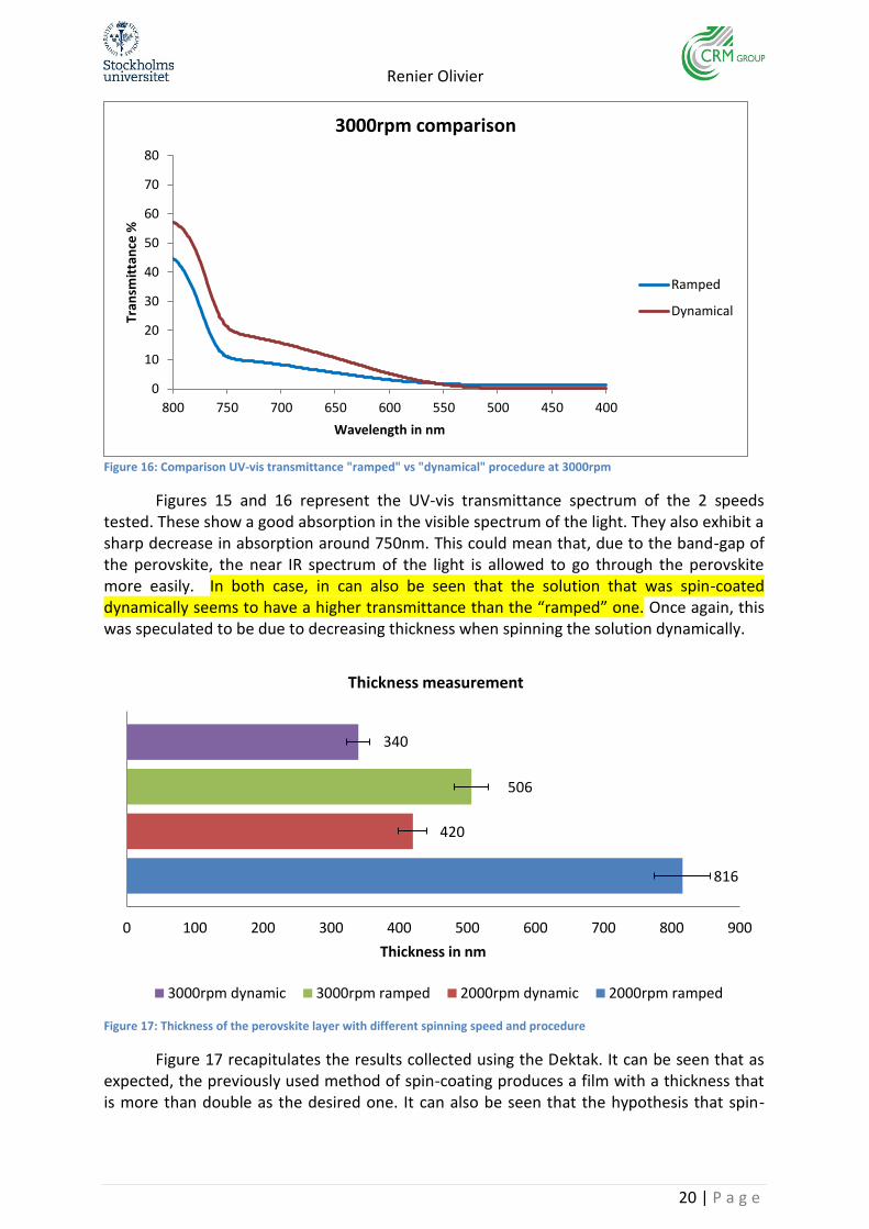
Figures 15 and 16 represent the UV-vis transmittance spectrum of the 2 speeds tested. These show a good absorption in the visible spectrum of the light. They also exhibit a sharp decrease in absorption around 750nm. This could mean that, due to the band-gap of the perovskite, the near IR spectrum of the light is allowed to go through the perovskite more easily. In both case, in can also be seen that the solution that was spin-coated dynamically seems to have a higher transmittance than the “ramped” one. Once again, this was speculated to be due to decreasing thickness when spinning the solution dynamically.
Figure 17: Thickness of the perovskite layer with different spinning speed and procedure
Figure 17 recapitulates the results collected using the Dektak. It can be seen that as expected, the previously used method of spin-coating produces a film with a thickness that is more than double as the desired one. It can also be seen that the hypothesis that spin-
0
10
20
30
40
50
60
70
80
800 750 700 650 600 550 500 450 400
Tran
smit
tan
ce %
Wavelength in nm
3000rpm comparison
Ramped
Dynamical
816
420
506
340
0 100 200 300 400 500 600 700 800 900
Thickness in nm
Thickness measurement
3000rpm dynamic 3000rpm ramped 2000rpm dynamic 2000rpm ramped
Renier Olivier
21 | P a g e
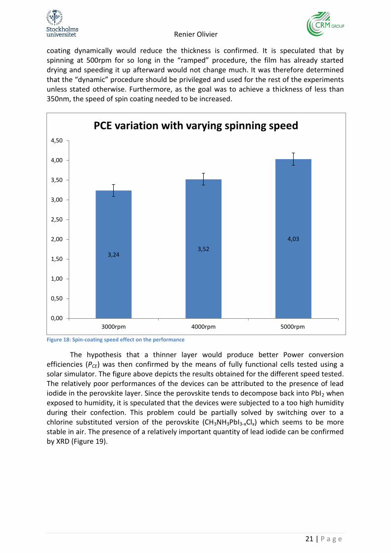
coating dynamically would reduce the thickness is confirmed. It is speculated that by spinning at 500rpm for so long in the “ramped” procedure, the film has already started drying and speeding it up afterward would not change much. It was therefore determined that the “dynamic” procedure should be privileged and used for the rest of the experiments unless stated otherwise. Furthermore, as the goal was to achieve a thickness of less than 350nm, the speed of spin coating needed to be increased.
Figure 18: Spin-coating speed effect on the performance
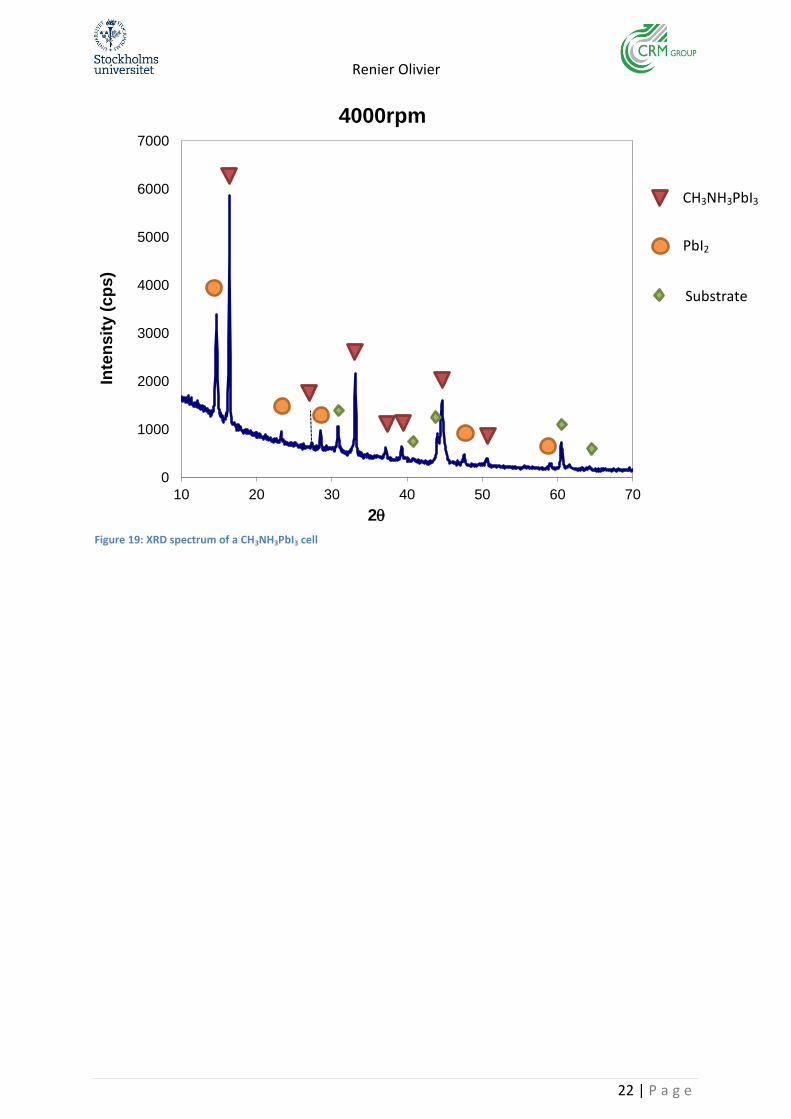
The hypothesis that a thinner layer would produce better Power conversion efficiencies (PCE) was then confirmed by the means of fully functional cells tested using a solar simulator. The figure above depicts the results obtained for the different speed tested. The relatively poor performances of the devices can be attributed to the presence of lead iodide in the perovskite layer. Since the perovskite tends to decompose back into PbI2 when exposed to humidity, it is speculated that the devices were subjected to a too high humidity during their confection. This problem could be partially solved by switching over to a chlorine substituted version of the perovskite (CH3NH3PbI3-xClx) which seems to be more stable in air. The presence of a relatively important quantity of lead iodide can be confirmed by XRD (Figure 19).
3,24 3,52
4,03
0,00
0,50
1,00
1,50
2,00
2,50
3,00
3,50
4,00
4,50
3000rpm 4000rpm 5000rpm
PCE variation with varying spinning speed
Renier Olivier
22 | P a g e
Figure 19: XRD spectrum of a CH3NH3PbI3 cell
0
1000
2000
3000
4000
5000
6000
7000
10 20 30 40 50 60 70
Inte
ns
ity (
cp
s)
2q
4000rpm
CH3NH3PbI3
PbI2
CH3NH3PbI3
Substrate
CH3NH3PbI3
Renier Olivier
23 | P a g e
2.2 1 Step procedure + anti-solvent
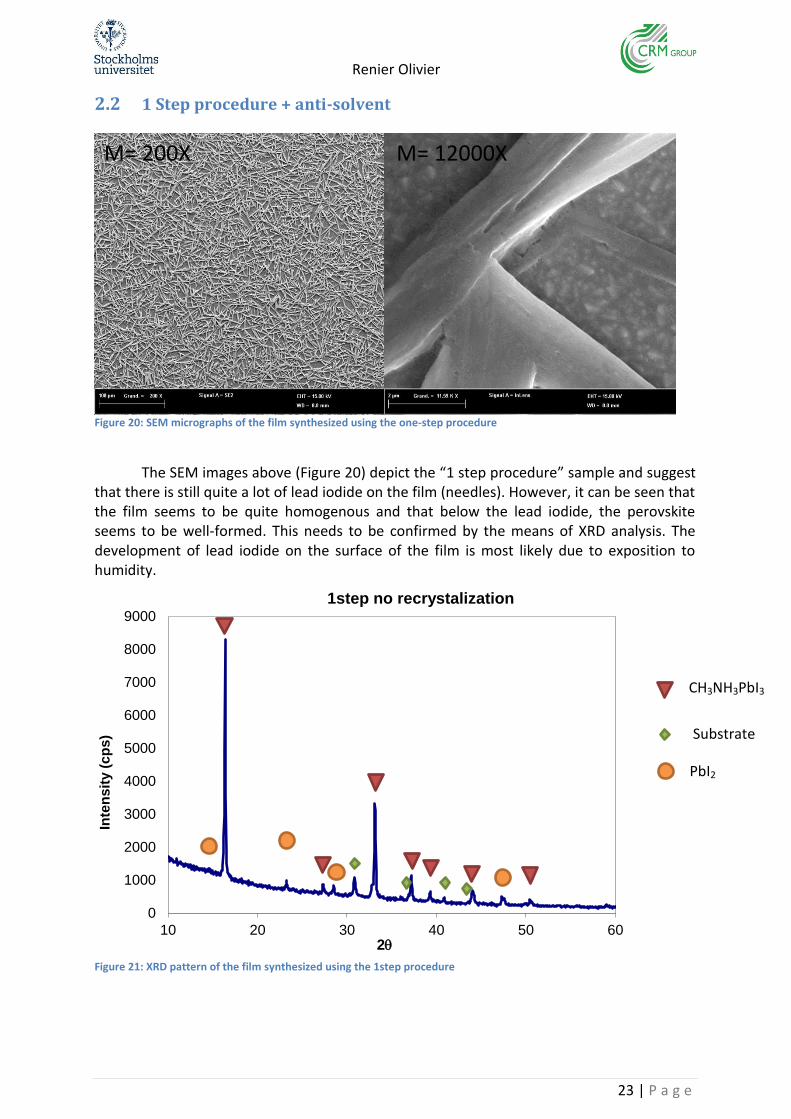
Figure 20: SEM micrographs of the film synthesized using the one-step procedure
The SEM images above (Figure 20) depict the “1 step procedure” sample and suggest
that there is still quite a lot of lead iodide on the film (needles). However, it can be seen that the film seems to be quite homogenous and that below the lead iodide, the perovskite seems to be well-formed. This needs to be confirmed by the means of XRD analysis. The development of lead iodide on the surface of the film is most likely due to exposition to humidity.
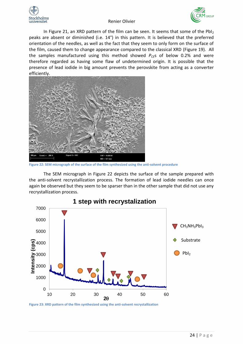
Figure 21: XRD pattern of the film synthesized using the 1step procedure
0
1000
2000
3000
4000
5000
6000
7000
8000
9000
10 20 30 40 50 60
Inte
nsit
y (
cp
s)
2q
1step no recrystalization
M= 200X M= 12000X
CH3NH3PbI3
PbI2
CH3NH3PbI3
Substrate
CH3NH3PbI3
Renier Olivier
24 | P a g e
In Figure 21, an XRD pattern of the film can be seen. It seems that some of the PbI2
peaks are absent or diminished (i.e. 14°) in this pattern. It is believed that the preferred orientation of the needles, as well as the fact that they seem to only form on the surface of the film, caused them to change appearance compared to the classical XRD (Figure 19). All the samples manufactured using this method showed PCEs of below 0.2% and were therefore regarded as having some flaw of undetermined origin. It is possible that the presence of lead iodide in big amount prevents the perovskite from acting as a converter efficiently.
Figure 22: SEM micrograph of the surface of the film synthesized using the anti-solvent procedure
The SEM micrograph in Figure 22 depicts the surface of the sample prepared with the anti-solvent recrystallization process. The formation of lead iodide needles can once again be observed but they seem to be sparser than in the other sample that did not use any recrystallization process.
Figure 23: XRD pattern of the film synthesized using the anti-solvent recrystallization
0
1000
2000
3000
4000
5000
6000
7000
10 20 30 40 50 60
Inte
ns
ity (
cp
s)
2q
1 step with recrystalization
PbI2
CH3NH3PbI3
CH3NH3PbI3
Substrate
CH3NH3PbI3
Renier Olivier
25 | P a g e
Figure 23 represent XRD pattern of the sample using the recrystallization process. Once again, some of the lead iodide peaks seem to be weaker. The explanation as to why they are weaker remains the same as previously stated.
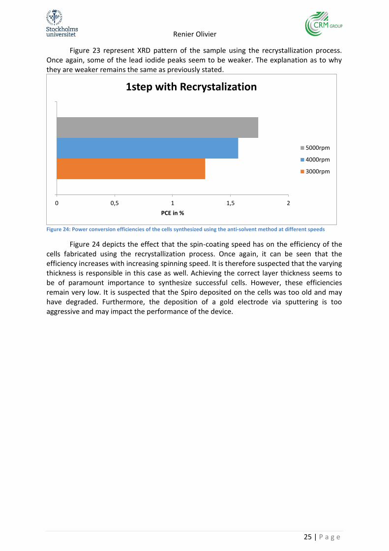
Figure 24: Power conversion efficiencies of the cells synthesized using the anti-solvent method at different speeds
Figure 24 depicts the effect that the spin-coating speed has on the efficiency of the cells fabricated using the recrystallization process. Once again, it can be seen that the efficiency increases with increasing spinning speed. It is therefore suspected that the varying thickness is responsible in this case as well. Achieving the correct layer thickness seems to be of paramount importance to synthesize successful cells. However, these efficiencies remain very low. It is suspected that the Spiro deposited on the cells was too old and may have degraded. Furthermore, the deposition of a gold electrode via sputtering is too aggressive and may impact the performance of the device.
0 0,5 1 1,5 2
PCE in %
1step with Recrystalization
5000rpm
4000rpm
3000rpm
Renier Olivier
26 | P a g e
2.3 Commercial solution
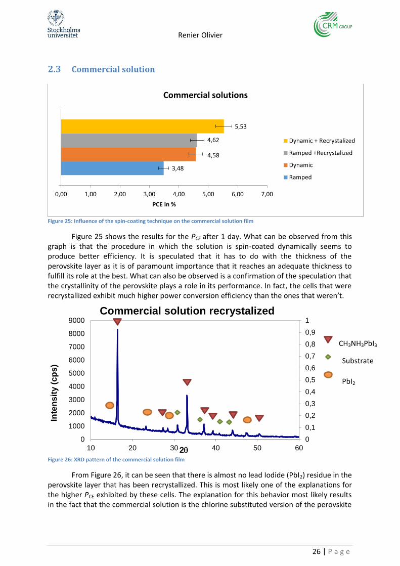
Figure 25: Influence of the spin-coating technique on the commercial solution film
Figure 25 shows the results for the PCE after 1 day. What can be observed from this graph is that the procedure in which the solution is spin-coated dynamically seems to produce better efficiency. It is speculated that it has to do with the thickness of the perovskite layer as it is of paramount importance that it reaches an adequate thickness to fulfill its role at the best. What can also be observed is a confirmation of the speculation that the crystallinity of the perovskite plays a role in its performance. In fact, the cells that were recrystallized exhibit much higher power conversion efficiency than the ones that weren’t.
Figure 26: XRD pattern of the commercial solution film
From Figure 26, it can be seen that there is almost no lead Iodide (PbI2) residue in the perovskite layer that has been recrystallized. This is most likely one of the explanations for the higher PCE exhibited by these cells. The explanation for this behavior most likely results in the fact that the commercial solution is the chlorine substituted version of the perovskite
3,48
4,58
4,62
5,53
0,00 1,00 2,00 3,00 4,00 5,00 6,00 7,00
PCE in %
Commercial solutions
Dynamic + Recrystalized
Ramped +Recrystalized
Dynamic
Ramped
0
0,1
0,2
0,3
0,4
0,5
0,6
0,7
0,8
0,9
1
0
1000
2000
3000
4000
5000
6000
7000
8000
9000
10 20 30 40 50 60
Inte
ns
ity (
cp
s)
2q
Commercial solution recrystalized
CH3NH3PbI3
Substrate
CH3NH3PbI3
PbI2
CH3NH3PbI3
Renier Olivier
27 | P a g e
(CH3NH3PbI3-xClx) which is said to be more stable and processable in air. For this reason, all further experiments will be conducted on the “substituted version” incorporating chlorine.
2.4 CH3NH3PbI3-xClx
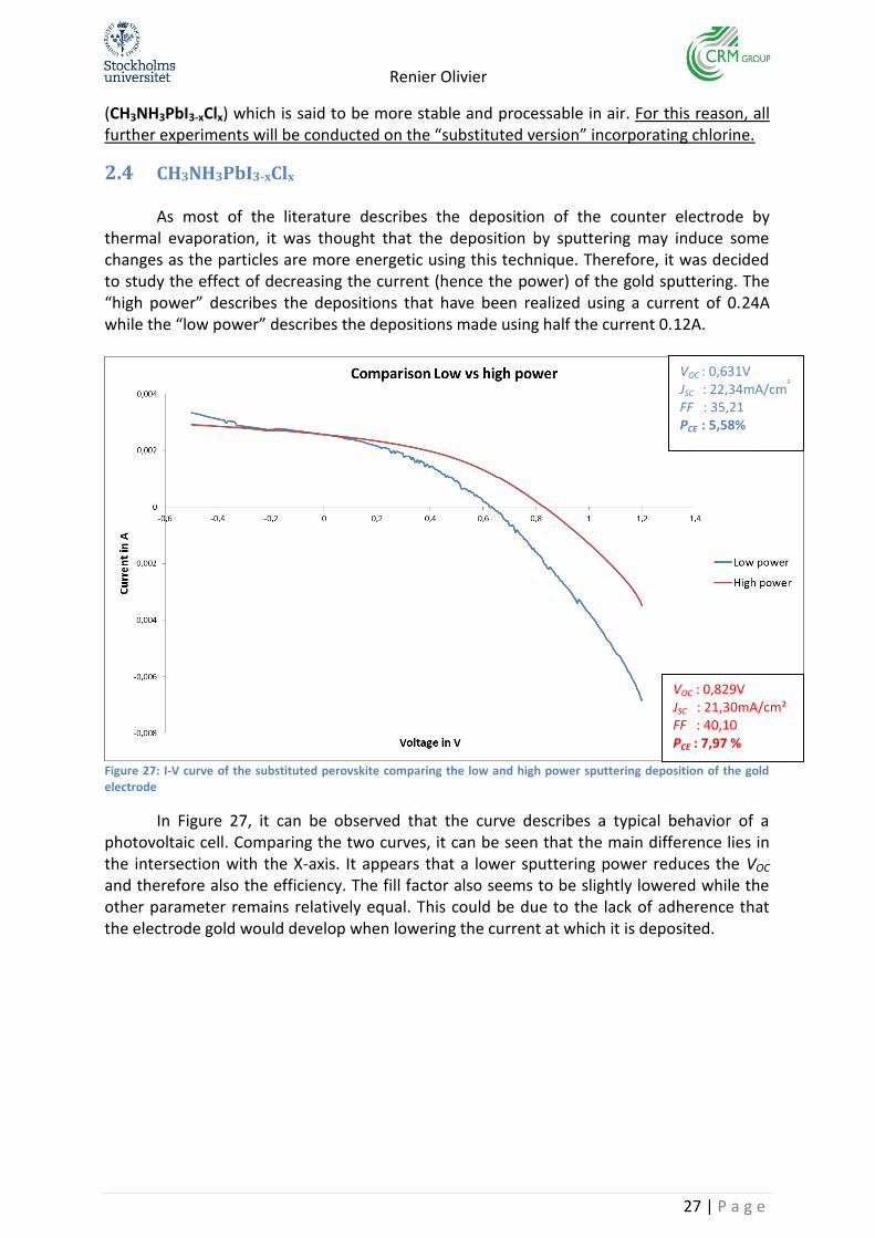
As most of the literature describes the deposition of the counter electrode by
thermal evaporation, it was thought that the deposition by sputtering may induce some changes as the particles are more energetic using this technique. Therefore, it was decided to study the effect of decreasing the current (hence the power) of the gold sputtering. The “high power” describes the depositions that have been realized using a current of 0.24A while the “low power” describes the depositions made using half the current 0.12A.
Figure 27: I-V curve of the substituted perovskite comparing the low and high power sputtering deposition of the gold electrode
In Figure 27, it can be observed that the curve describes a typical behavior of a photovoltaic cell. Comparing the two curves, it can be seen that the main difference lies in the intersection with the X-axis. It appears that a lower sputtering power reduces the VOC and therefore also the efficiency. The fill factor also seems to be slightly lowered while the other parameter remains relatively equal. This could be due to the lack of adherence that the electrode gold would develop when lowering the current at which it is deposited.
VOC : 0,829V JSC : 21,30mA/cm² FF : 40,10 PCE : 7,97 %
VOC : 0,631V JSC : 22,34mA/cm
²
FF : 35,21 PCE : 5,58%
Renier Olivier
28 | P a g e
2.5 SEM study
Figure 28: Comparison of the surface morphology of the Substituted and DIO procedure (magnification: 50 X and 100k X)
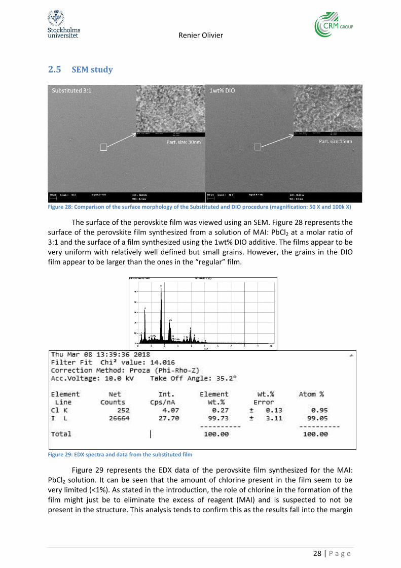
The surface of the perovskite film was viewed using an SEM. Figure 28 represents the surface of the perovskite film synthesized from a solution of MAI: PbCl2 at a molar ratio of 3:1 and the surface of a film synthesized using the 1wt% DIO additive. The films appear to be very uniform with relatively well defined but small grains. However, the grains in the DIO film appear to be larger than the ones in the “regular” film.
Figure 29: EDX spectra and data from the substituted film
Figure 29 represents the EDX data of the perovskite film synthesized for the MAI: PbCl2 solution. It can be seen that the amount of chlorine present in the film seem to be very limited (<1%). As stated in the introduction, the role of chlorine in the formation of the film might just be to eliminate the excess of reagent (MAI) and is suspected to not be present in the structure. This analysis tends to confirm this as the results fall into the margin
Renier Olivier
29 | P a g e
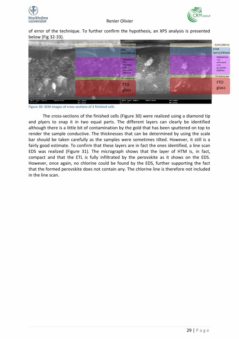
of error of the technique. To further confirm the hypothesis, an XPS analysis is presented below (Fig 32-33).
Figure 30: SEM images of cross sections of 2 finished cells
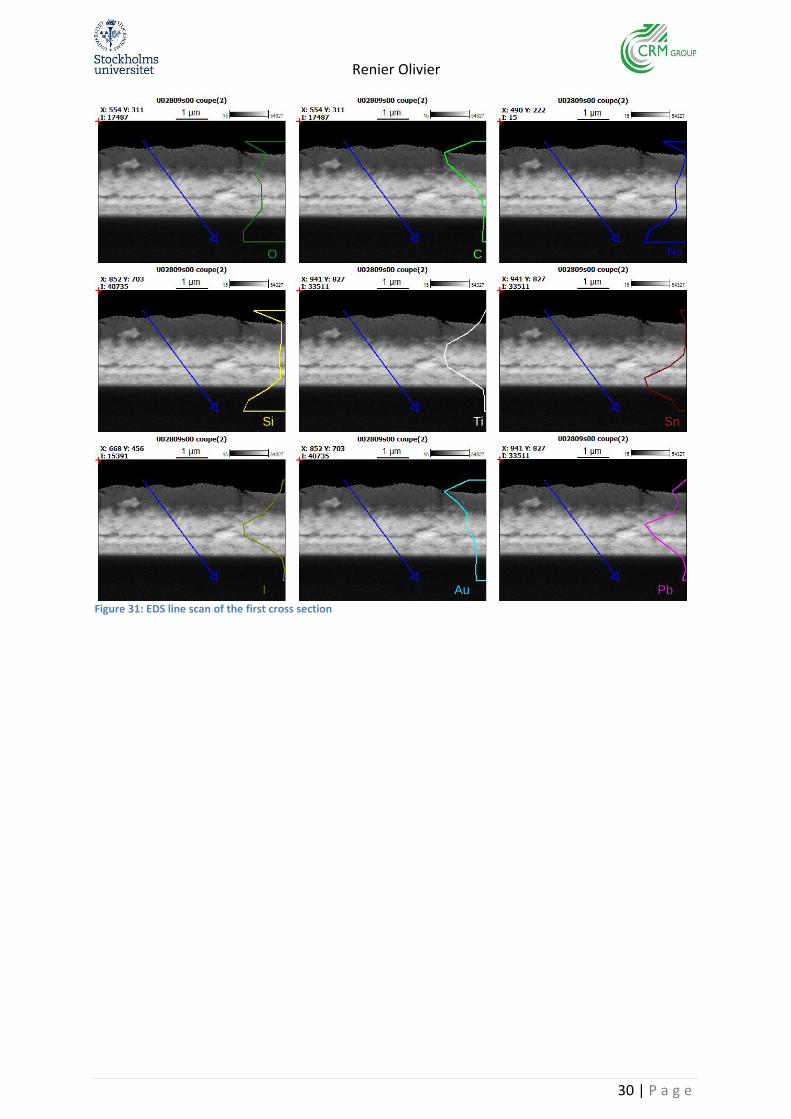
The cross-sections of the finished cells (Figure 30) were realized using a diamond tip and plyers to snap it in two equal parts. The different layers can clearly be identified although there is a little bit of contamination by the gold that has been sputtered on top to render the sample conductive. The thicknesses that can be determined by using the scale bar should be taken carefully as the samples were sometimes tilted. However, it still is a fairly good estimate. To confirm that these layers are in fact the ones identified, a line scan EDS was realized (Figure 31). The micrograph shows that the layer of HTM is, in fact, compact and that the ETL is fully infiltrated by the perovskite as it shows on the EDS. However, once again, no chlorine could be found by the EDS, further supporting the fact that the formed perovskite does not contain any. The chlorine line is therefore not included in the line scan.
Renier Olivier
30 | P a g e
Figure 31: EDS line scan of the first cross section
O C Na
Si Ti Sn
I Au Pb
Renier Olivier
31 | P a g e
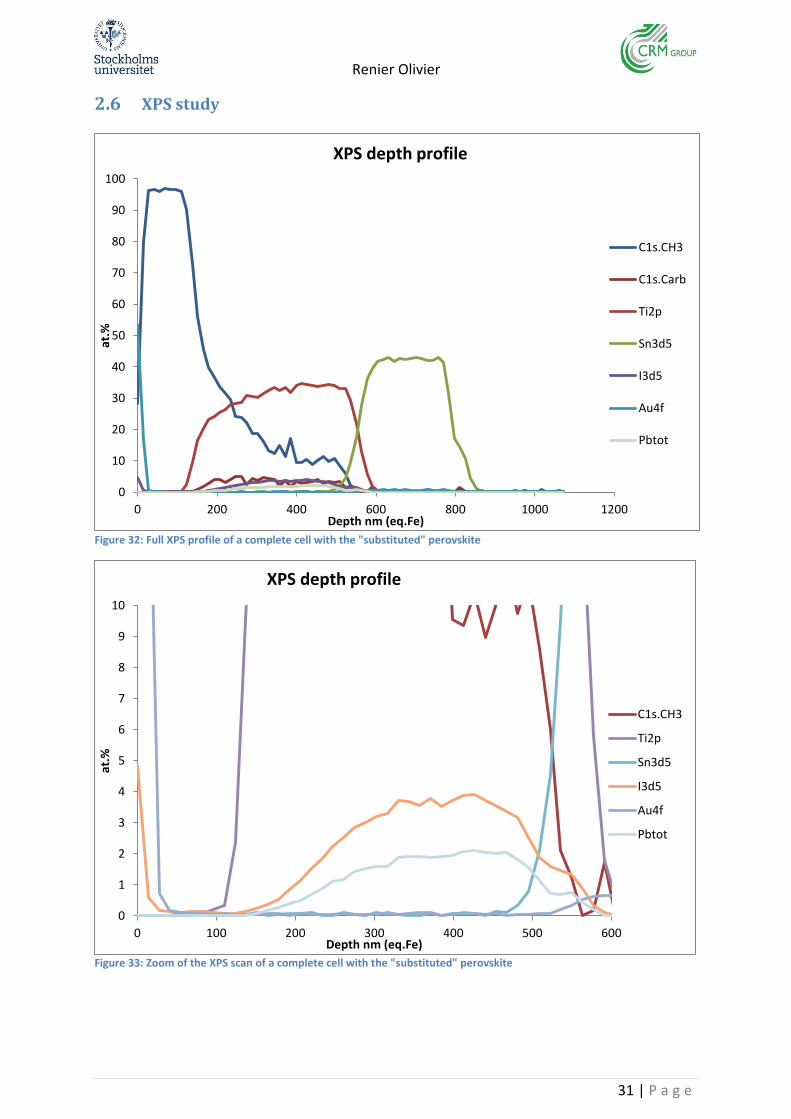
2.6 XPS study
Figure 32: Full XPS profile of a complete cell with the "substituted" perovskite
Figure 33: Zoom of the XPS scan of a complete cell with the "substituted" perovskite
0
10
20
30
40
50
60
70
80
90
100
0 200 400 600 800 1000 1200
at.%
Depth nm (eq.Fe)
XPS depth profile
C1s.CH3
C1s.Carb
Ti2p
Sn3d5
I3d5
Au4f
Pbtot
0
1
2
3
4
5
6
7
8
9
10
0 100 200 300 400 500 600
at.%
Depth nm (eq.Fe)
XPS depth profile
C1s.CH3
Ti2p
Sn3d5
I3d5
Au4f
Pbtot
Renier Olivier
32 | P a g e
No trace of chlorine was present during the XPS analysis of the perovskite film which confirms the hypothesis that it only plays a role of reagent’s excess eliminator rather than a substituent for the iodide in the perovskite structure. Furthermore, this analysis allows for a more accurate measurement of the thickness of each layer. The layer of Spiro appears to be ±160nm thick while the perovskite layer (containing lead and Iodide) ±450nm. This is also the case of the TiO2 layer that is fully infiltrated by the perovskite. The FTO layer appears to be at least 300nm thick
2.7 Influence of Corona treatment
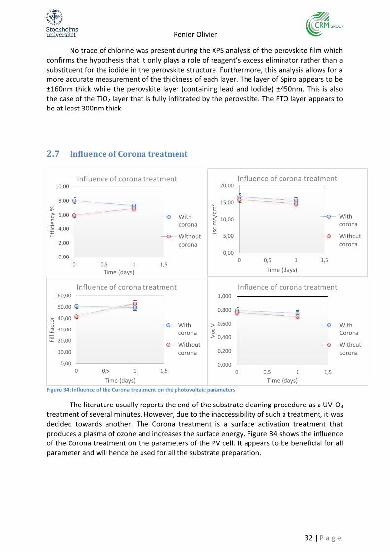
Figure 34: Influence of the Corona treatment on the photovoltaic parameters
The literature usually reports the end of the substrate cleaning procedure as a UV-O3 treatment of several minutes. However, due to the inaccessibility of such a treatment, it was decided towards another. The Corona treatment is a surface activation treatment that produces a plasma of ozone and increases the surface energy. Figure 34 shows the influence of the Corona treatment on the parameters of the PV cell. It appears to be beneficial for all parameter and will hence be used for all the substrate preparation.
0,000
0,200
0,400
0,600
0,800
1,000
0 0,5 1 1,5
Vo
c V
Time (days)
Influence of corona treatment
WithCorona
Withoutcorona
0,00
5,00
10,00
15,00
20,00
0 0,5 1 1,5
Jsc
mA
/cm
²
Time (days)
Influence of corona treatment
Withcorona
Withoutcorona
0,00
10,00
20,00
30,00
40,00
50,00
60,00
0 0,5 1 1,5
Fill
Fact
or
Time (days)
Influence of corona treatment
Withcorona
Withoutcorona
0,00
2,00
4,00
6,00
8,00
10,00
0 0,5 1 1,5
Effi
cien
cy %
Time (days)
Influence of corona treatment
Withcorona
Withoutcorona
Renier Olivier
33 | P a g e
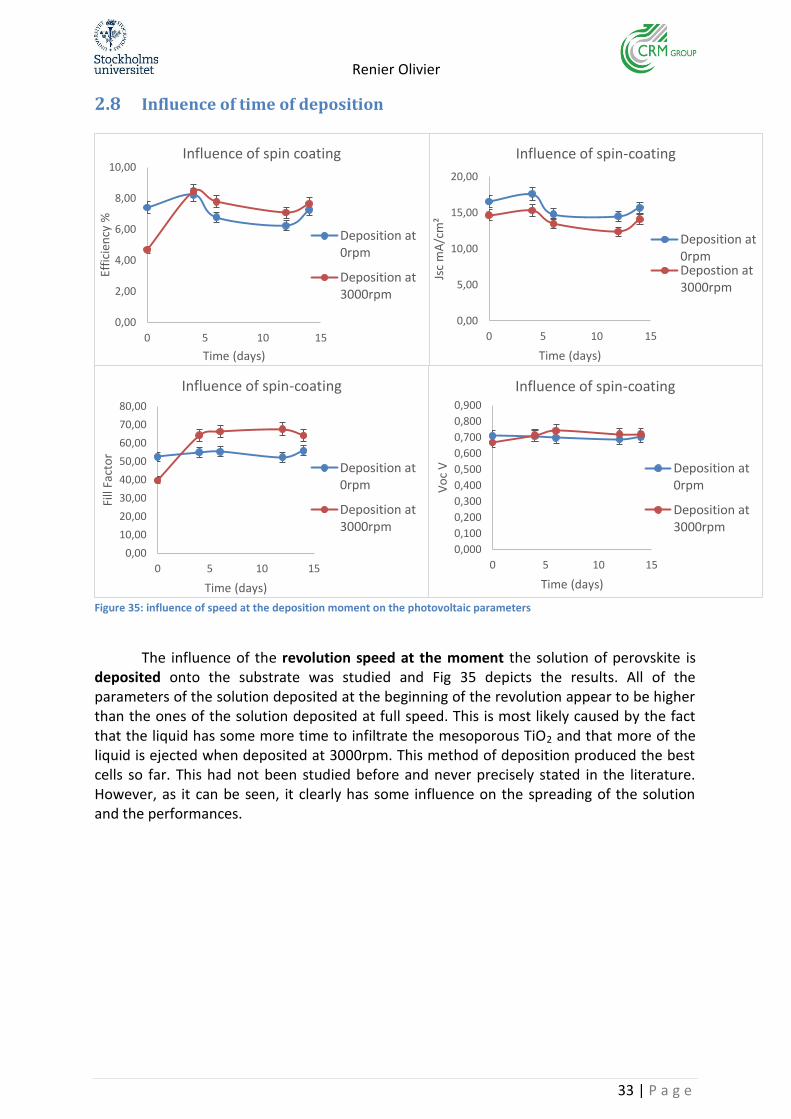
2.8 Influence of time of deposition
Figure 35: influence of speed at the deposition moment on the photovoltaic parameters
The influence of the revolution speed at the moment the solution of perovskite is
deposited onto the substrate was studied and Fig 35 depicts the results. All of the parameters of the solution deposited at the beginning of the revolution appear to be higher than the ones of the solution deposited at full speed. This is most likely caused by the fact that the liquid has some more time to infiltrate the mesoporous TiO2 and that more of the liquid is ejected when deposited at 3000rpm. This method of deposition produced the best cells so far. This had not been studied before and never precisely stated in the literature. However, as it can be seen, it clearly has some influence on the spreading of the solution and the performances.
0,000
0,100
0,200
0,300
0,400
0,500
0,600
0,700
0,800
0,900
0 5 10 15
Vo
c V
Time (days)
Influence of spin-coating
Deposition at0rpm
Deposition at3000rpm
0,00
5,00
10,00
15,00
20,00
0 5 10 15
Jsc
mA
/cm
²
Time (days)
Influence of spin-coating
Deposition at0rpmDepostion at3000rpm
0,00
10,00
20,00
30,00
40,00
50,00
60,00
70,00
80,00
0 5 10 15
Fill
Fact
or
Time (days)
Influence of spin-coating
Deposition at0rpm
Deposition at3000rpm
0,00
2,00
4,00
6,00
8,00
10,00
0 5 10 15
Effi
cien
cy %
Time (days)
Influence of spin coating
Deposition at0rpm
Deposition at3000rpm
Renier Olivier
34 | P a g e
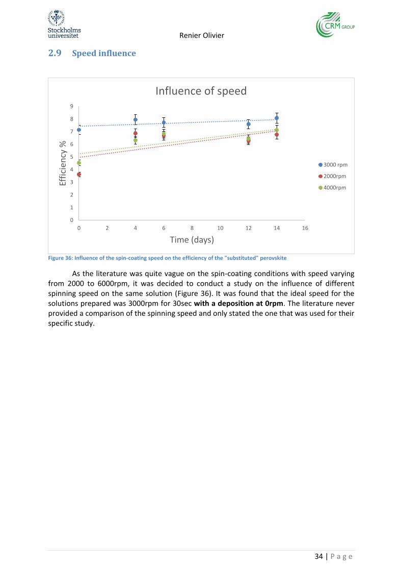
2.9 Speed influence
Figure 36: Influence of the spin-coating speed on the efficiency of the "substituted" perovskite
As the literature was quite vague on the spin-coating conditions with speed varying from 2000 to 6000rpm, it was decided to conduct a study on the influence of different spinning speed on the same solution (Figure 36). It was found that the ideal speed for the solutions prepared was 3000rpm for 30sec with a deposition at 0rpm. The literature never provided a comparison of the spinning speed and only stated the one that was used for their specific study.
0
1
2
3
4
5
6
7
8
9
0 2 4 6 8 10 12 14 16
Effi
cien
cy %
Time (days)
Influence of speed
3000 rpm
2000rpm
4000rpm
Renier Olivier
35 | P a g e
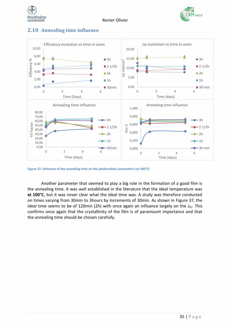
2.10 Annealing time influence
Figure 37: Influence of the annealing time on the photovoltaic parameters (at 100°C)
Another parameter that seemed to play a big role in the formation of a good film is
the annealing time. It was well established in the literature that the ideal temperature was at 100°C, but it was never clear what the ideal time was. A study was therefore conducted on times varying from 30min to 3hours by increments of 30min. As shown in Figure 37, the ideal time seems to be of 120min (2h) with once again an influence largely on the JSC. This confirms once again that the crystallinity of the film is of paramount importance and that the annealing time should be chosen carefully.
0,000
0,200
0,400
0,600
0,800
1,000
0 2 4 6
Vo
c V
Time (days)
Annealing time influence
3h
2 1/2h
2h
1h
30 min
0,00
5,00
10,00
15,00
20,00
0 2 4 6
Jsc
mA
/cm
²
Time (days)
Jsc evolution vs time in oven
3h
2 1/2h
2h
1h
30 min
0,0010,0020,0030,0040,0050,0060,0070,0080,00
0 2 4 6
Fill
Fact
or
Time (days)
Annealing time influence
3h
2 1/2h
2h
1h
30min
0,00
2,00
4,00
6,00
8,00
10,00
0 2 4 6
Effi
cien
cy %
Time (Days)
Efficiency evolution vs time in oven
3h
2 1/2h
2h
1h
30min
Renier Olivier
36 | P a g e
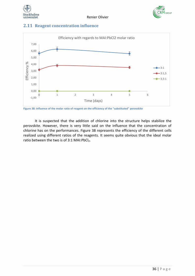
2.11 Reagent concentration influence
Figure 38: Influence of the molar ratio of reagent on the efficiency of the "substituted" perovskite
It is suspected that the addition of chlorine into the structure helps stabilize the
perovskite. However, there is very little said on the influence that the concentration of chlorine has on the performances. Figure 38 represents the efficiency of the different cells realized using different ratios of the reagents. It seems quite obvious that the ideal molar ratio between the two is of 3:1 MAI:PbCl2.
-1,00
0,00
1,00
2,00
3,00
4,00
5,00
6,00
7,00
0 1 2 3 4 5 6
Effi
cien
cy %
Time (days)
Efficiency with regards to MAI:PbCl2 molar ratio
3:1
3:1,5
3,5:1
Renier Olivier
37 | P a g e
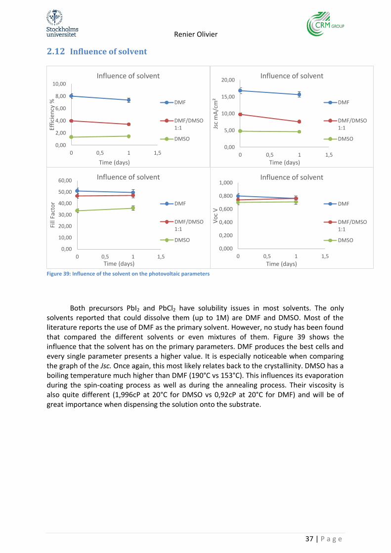
2.12 Influence of solvent
Figure 39: Influence of the solvent on the photovoltaic parameters
Both precursors PbI2 and PbCl2 have solubility issues in most solvents. The only solvents reported that could dissolve them (up to 1M) are DMF and DMSO. Most of the literature reports the use of DMF as the primary solvent. However, no study has been found that compared the different solvents or even mixtures of them. Figure 39 shows the influence that the solvent has on the primary parameters. DMF produces the best cells and every single parameter presents a higher value. It is especially noticeable when comparing the graph of the Jsc. Once again, this most likely relates back to the crystallinity. DMSO has a boiling temperature much higher than DMF (190°C vs 153°C). This influences its evaporation during the spin-coating process as well as during the annealing process. Their viscosity is also quite different (1,996cP at 20°C for DMSO vs 0,92cP at 20°C for DMF) and will be of great importance when dispensing the solution onto the substrate.
0,000
0,200
0,400
0,600
0,800
1,000
0 0,5 1 1,5
Vo
c V
Time (days)
Influence of solvent
DMF
DMF/DMSO1:1
DMSO
0,00
5,00
10,00
15,00
20,00
0 0,5 1 1,5
Jsc
mA
/cm
²
Time (days)
Influence of solvent
DMF
DMF/DMSO1:1
DMSO
0,00
10,00
20,00
30,00
40,00
50,00
60,00
0 0,5 1 1,5
Fill
Fact
or
Time (days)
Influence of solvent
DMF
DMF/DMSO1:1
DMSO
0,00
2,00
4,00
6,00
8,00
10,00
0 0,5 1 1,5
Effi
cien
cy %
Time (days)
Influence of solvent
DMF
DMF/DMSO1:1
DMSO
Renier Olivier
38 | P a g e
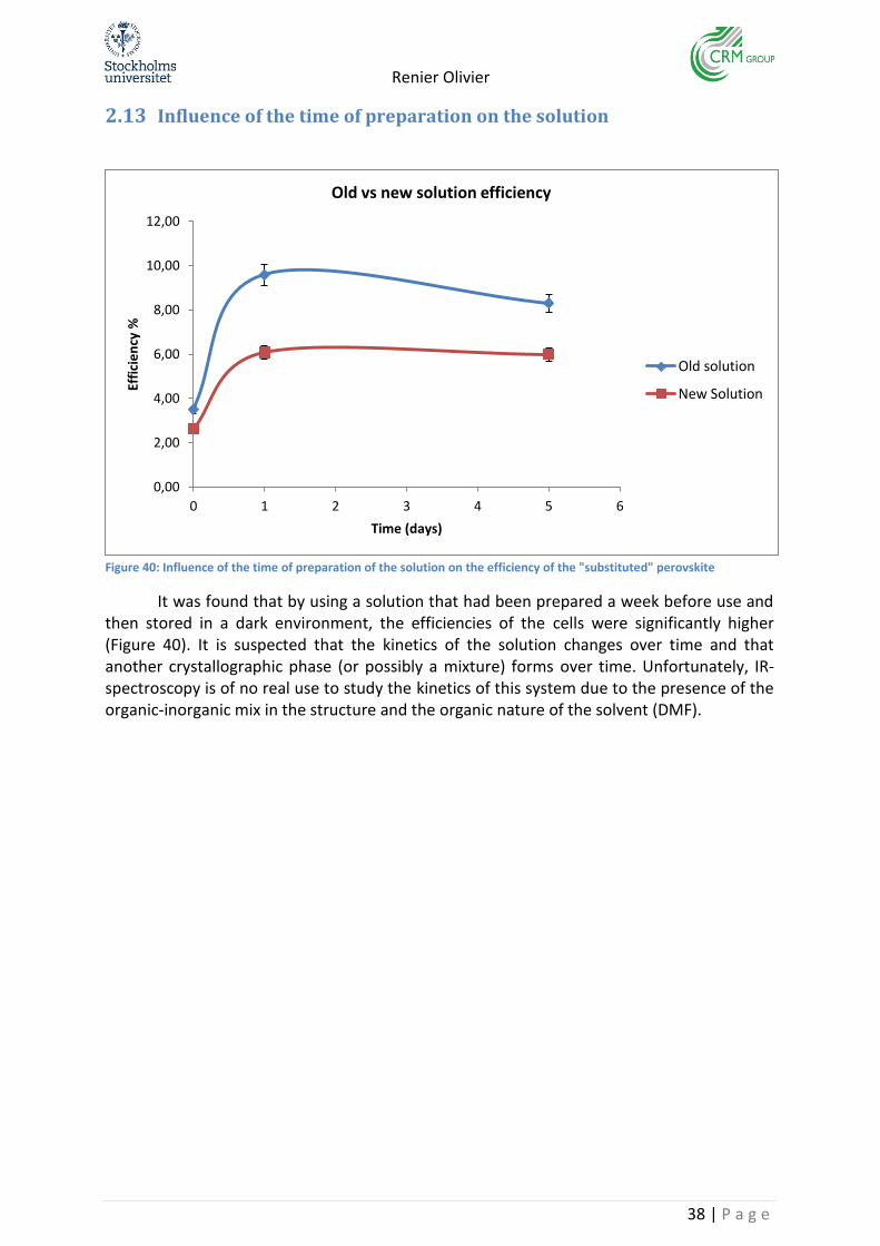
2.13 Influence of the time of preparation on the solution
Figure 40: Influence of the time of preparation of the solution on the efficiency of the "substituted" perovskite
It was found that by using a solution that had been prepared a week before use and then stored in a dark environment, the efficiencies of the cells were significantly higher (Figure 40). It is suspected that the kinetics of the solution changes over time and that another crystallographic phase (or possibly a mixture) forms over time. Unfortunately, IR-spectroscopy is of no real use to study the kinetics of this system due to the presence of the organic-inorganic mix in the structure and the organic nature of the solvent (DMF).
0,00
2,00
4,00
6,00
8,00
10,00
12,00
0 1 2 3 4 5 6
Effi
cie
ncy
%
Time (days)
Old vs new solution efficiency
Old solution
New Solution
Renier Olivier
39 | P a g e
2.14 Enhanced crystallization using 1,8 Diiodooctane (DIO)
1,8 Diiodooctane (DIO) acts as a chelation agent. This bidentate halogenated additive has the capacity to temporarily chelate Pb2+ during the crystallization. This can be observed immediately as the solubility of PbCl2 increases in the presence of this additive. The chelation promotes a more homogenous nucleation and most likely modifies the interfacial energy in favorable ways which in turns affects the crystal growth. Therefore, the film should exhibit a more homogeneous structure and ultimately increase the fill factor. 1wt% (with regards to the perovskite) of this additive was added to the perovskite solution.
Figure 41: Comparison of the low and high power gold sputtering for the DIO recrystallization procedure
As it can be seen in Figure 41, the low power sputtering seems to be beneficiary for
the DIO procedure. This is believed to be because of the modifications to the surface of the perovskite film which will in turn influence the surface of the film of Spiro deposited on top. This will hence, influence the surface roughness and promote the adherence of gold with lower power. It can also be seen that the parameters seem to be improving. Table 1: Summary of the relevant parameters
Type Voc in V Jsc in mA/cm² FF PCE in %
Substituted low power
0.632
22.34 35.21 5.58
Substituted high power
0.829 21.3 40.1 7.97
DIO low power 0.77 23.65 39.62 8.12
DIO high power 0.7 18.39 37.16 5.43
VOC : 0,707V JSC : 18,39mA/cm² FF : 37,16 PCE : 5,43%
VOC : 0,770V JSC : 23,65mA/cm² FF : 39,62 PCE : 8,12%
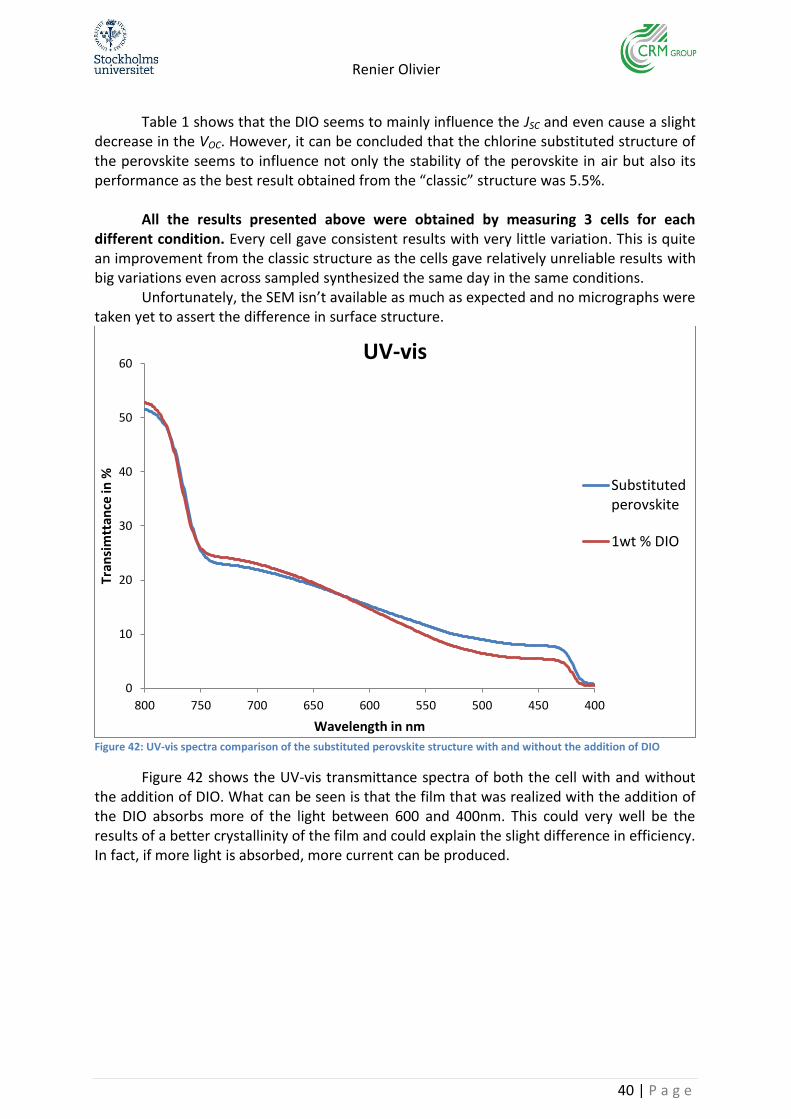
Renier Olivier
40 | P a g e
Table 1 shows that the DIO seems to mainly influence the JSC and even cause a slight
decrease in the VOC. However, it can be concluded that the chlorine substituted structure of the perovskite seems to influence not only the stability of the perovskite in air but also its performance as the best result obtained from the “classic” structure was 5.5%.
All the results presented above were obtained by measuring 3 cells for each different condition. Every cell gave consistent results with very little variation. This is quite an improvement from the classic structure as the cells gave relatively unreliable results with big variations even across sampled synthesized the same day in the same conditions.
Unfortunately, the SEM isn’t available as much as expected and no micrographs were taken yet to assert the difference in surface structure.
Figure 42: UV-vis spectra comparison of the substituted perovskite structure with and without the addition of DIO
Figure 42 shows the UV-vis transmittance spectra of both the cell with and without the addition of DIO. What can be seen is that the film that was realized with the addition of the DIO absorbs more of the light between 600 and 400nm. This could very well be the results of a better crystallinity of the film and could explain the slight difference in efficiency. In fact, if more light is absorbed, more current can be produced.
0
10
20
30
40
50
60
400450500550600650700750800
Tran
sim
ttan
ce in
%
Wavelength in nm
UV-vis
Substitutedperovskite
1wt % DIO
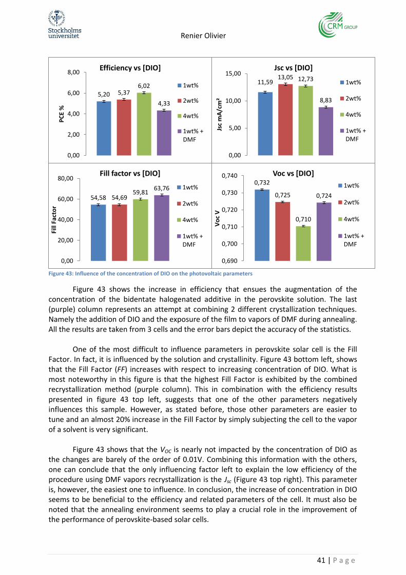
Renier Olivier
41 | P a g e
Figure 43: Influence of the concentration of DIO on the photovoltaic parameters
Figure 43 shows the increase in efficiency that ensues the augmentation of the concentration of the bidentate halogenated additive in the perovskite solution. The last (purple) column represents an attempt at combining 2 different crystallization techniques. Namely the addition of DIO and the exposure of the film to vapors of DMF during annealing. All the results are taken from 3 cells and the error bars depict the accuracy of the statistics.
One of the most difficult to influence parameters in perovskite solar cell is the Fill Factor. In fact, it is influenced by the solution and crystallinity. Figure 43 bottom left, shows that the Fill Factor (FF) increases with respect to increasing concentration of DIO. What is most noteworthy in this figure is that the highest Fill Factor is exhibited by the combined recrystallization method (purple column). This in combination with the efficiency results presented in figure 43 top left, suggests that one of the other parameters negatively influences this sample. However, as stated before, those other parameters are easier to tune and an almost 20% increase in the Fill Factor by simply subjecting the cell to the vapor of a solvent is very significant.
Figure 43 shows that the VOC is nearly not impacted by the concentration of DIO as the changes are barely of the order of 0.01V. Combining this information with the others, one can conclude that the only influencing factor left to explain the low efficiency of the procedure using DMF vapors recrystallization is the Jsc (Figure 43 top right). This parameter is, however, the easiest one to influence. In conclusion, the increase of concentration in DIO seems to be beneficial to the efficiency and related parameters of the cell. It must also be noted that the annealing environment seems to play a crucial role in the improvement of the performance of perovskite-based solar cells.
5,20 5,37 6,02
4,33
0,00
2,00
4,00
6,00
8,00
PC
E %
Efficiency vs [DIO]
1wt%
2wt%
4wt%
1wt% +DMF
54,58 54,69 59,81
63,76
0,00
20,00
40,00
60,00
80,00
Fill
Fact
or
Fill factor vs [DIO]
1wt%
2wt%
4wt%
1wt% +DMF
11,59 13,05 12,73
8,83
0,00
5,00
10,00
15,00
Jsc
mA
/cm
²
Jsc vs [DIO]
1wt%
2wt%
4wt%
1wt% +DMF
0,732
0,725
0,710
0,724
0,690
0,700
0,710
0,720
0,730
0,740
Vo
c V
Voc vs [DIO]
1wt%
2wt%
4wt%
1wt% +DMF
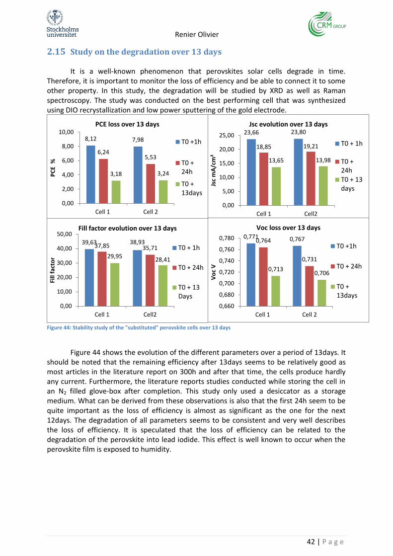
Renier Olivier
42 | P a g e
2.15 Study on the degradation over 13 days
It is a well-known phenomenon that perovskites solar cells degrade in time. Therefore, it is important to monitor the loss of efficiency and be able to connect it to some other property. In this study, the degradation will be studied by XRD as well as Raman spectroscopy. The study was conducted on the best performing cell that was synthesized using DIO recrystallization and low power sputtering of the gold electrode.
Figure 44: Stability study of the "substituted" perovskite cells over 13 days
Figure 44 shows the evolution of the different parameters over a period of 13days. It
should be noted that the remaining efficiency after 13days seems to be relatively good as most articles in the literature report on 300h and after that time, the cells produce hardly any current. Furthermore, the literature reports studies conducted while storing the cell in an N2 filled glove-box after completion. This study only used a desiccator as a storage medium. What can be derived from these observations is also that the first 24h seem to be quite important as the loss of efficiency is almost as significant as the one for the next 12days. The degradation of all parameters seems to be consistent and very well describes the loss of efficiency. It is speculated that the loss of efficiency can be related to the degradation of the perovskite into lead iodide. This effect is well known to occur when the perovskite film is exposed to humidity.
8,12 7,98
6,24 5,53
3,18 3,24
0,00
2,00
4,00
6,00
8,00
10,00
Cell 1 Cell 2
PC
E %
PCE loss over 13 days
T0 +1h
T0 +24h
T0 +13days
39,63 38,93 37,85 35,71
29,95 28,41
0,00
10,00
20,00
30,00
40,00
50,00
Cell 1 Cell2
Fill
fact
or
Fill factor evolution over 13 days
T0 + 1h
T0 + 24h
T0 + 13Days
23,66 23,80
18,85 19,21
13,65 13,98
0,00
5,00
10,00
15,00
20,00
25,00
Cell 1 Cell2Js
c m
A/c
m²
Jsc evolution over 13 days
T0 + 1h
T0 +24h
T0 + 13days
0,771 0,767 0,764
0,731
0,713 0,706
0,660
0,680
0,700
0,720
0,740
0,760
0,780
Cell 1 Cell 2
Vo
c V
Voc loss over 13 days
T0 +1h
T0 + 24h
T0 +13days
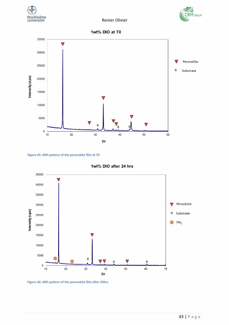
Renier Olivier
43 | P a g e
Figure 45: XRD pattern of the perovskite film at T0
Figure 46: XRD pattern of the perovskite film after 24hrs
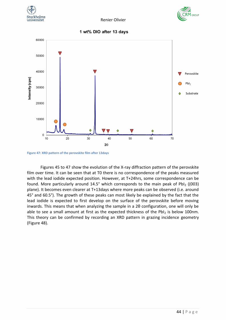
Renier Olivier
44 | P a g e
Figure 47: XRD pattern of the perovskite film after 13days
Figures 45 to 47 show the evolution of the X-ray diffraction pattern of the perovskite
film over time. It can be seen that at T0 there is no correspondence of the peaks measured with the lead iodide expected position. However, at T+24hrs, some correspondence can be found. More particularly around 14.5° which corresponds to the main peak of PbI2 ((003) plane). It becomes even clearer at T+13days where more peaks can be observed (i.e. around 45° and 60.5°). The growth of these peaks can most likely be explained by the fact that the lead iodide is expected to first develop on the surface of the perovskite before moving inwards. This means that when analyzing the sample in a 2θ configuration, one will only be able to see a small amount at first as the expected thickness of the PbI2 is below 100nm. This theory can be confirmed by recording an XRD pattern in grazing incidence geometry (Figure 48).
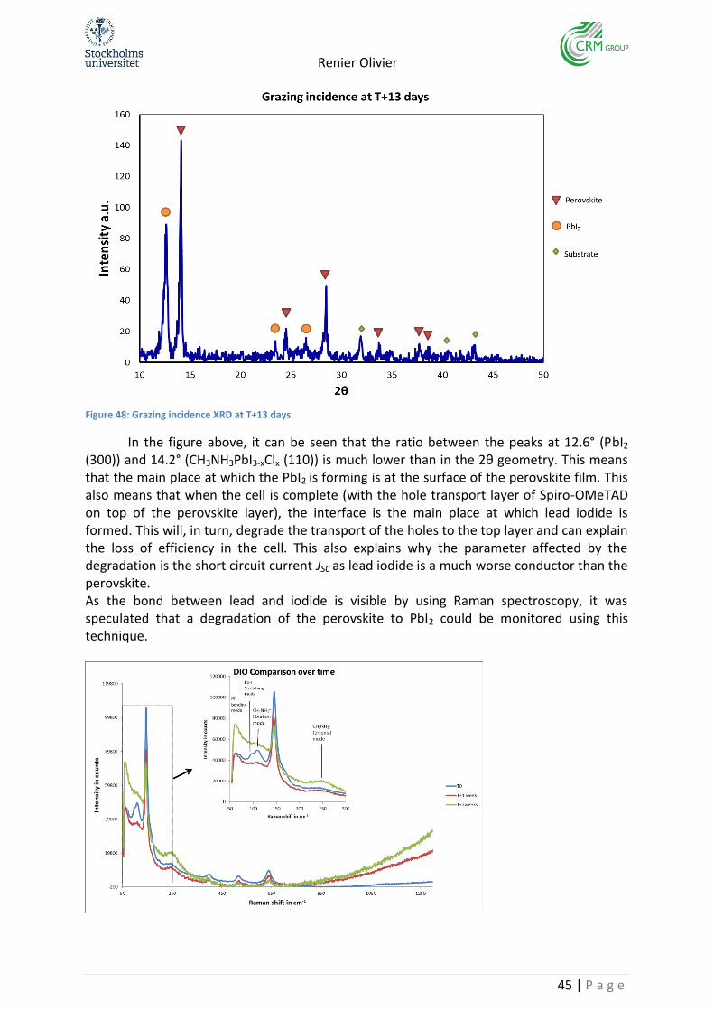
Renier Olivier
45 | P a g e
Figure 48: Grazing incidence XRD at T+13 days
In the figure above, it can be seen that the ratio between the peaks at 12.6° (PbI2 (300)) and 14.2° (CH3NH3PbI3-xClx (110)) is much lower than in the 2θ geometry. This means that the main place at which the PbI2 is forming is at the surface of the perovskite film. This also means that when the cell is complete (with the hole transport layer of Spiro-OMeTAD on top of the perovskite layer), the interface is the main place at which lead iodide is formed. This will, in turn, degrade the transport of the holes to the top layer and can explain the loss of efficiency in the cell. This also explains why the parameter affected by the degradation is the short circuit current JSC as lead iodide is a much worse conductor than the perovskite. As the bond between lead and iodide is visible by using Raman spectroscopy, it was speculated that a degradation of the perovskite to PbI2 could be monitored using this technique.
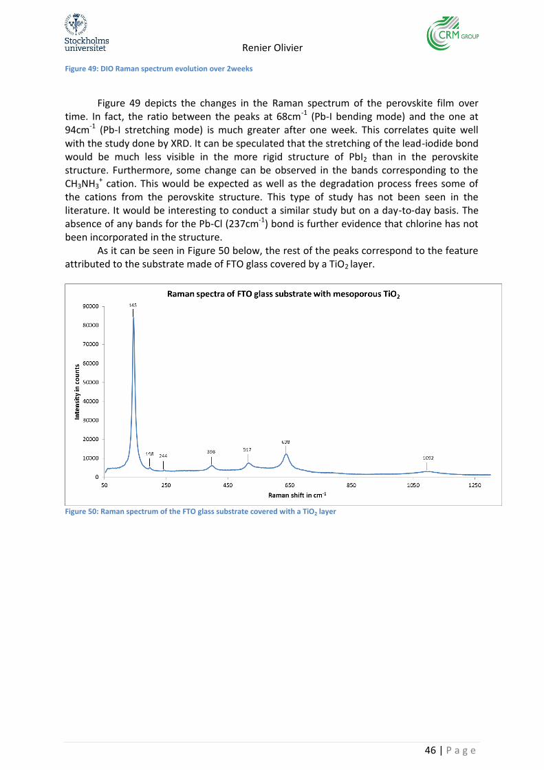
Renier Olivier
46 | P a g e
Figure 49: DIO Raman spectrum evolution over 2weeks
Figure 49 depicts the changes in the Raman spectrum of the perovskite film over
time. In fact, the ratio between the peaks at 68cm-1 (Pb-I bending mode) and the one at 94cm-1 (Pb-I stretching mode) is much greater after one week. This correlates quite well with the study done by XRD. It can be speculated that the stretching of the lead-iodide bond would be much less visible in the more rigid structure of PbI2 than in the perovskite structure. Furthermore, some change can be observed in the bands corresponding to the CH3NH3
+ cation. This would be expected as well as the degradation process frees some of the cations from the perovskite structure. This type of study has not been seen in the literature. It would be interesting to conduct a similar study but on a day-to-day basis. The absence of any bands for the Pb-Cl (237cm-1) bond is further evidence that chlorine has not been incorporated in the structure.
As it can be seen in Figure 50 below, the rest of the peaks correspond to the feature attributed to the substrate made of FTO glass covered by a TiO2 layer.
Figure 50: Raman spectrum of the FTO glass substrate covered with a TiO2 layer
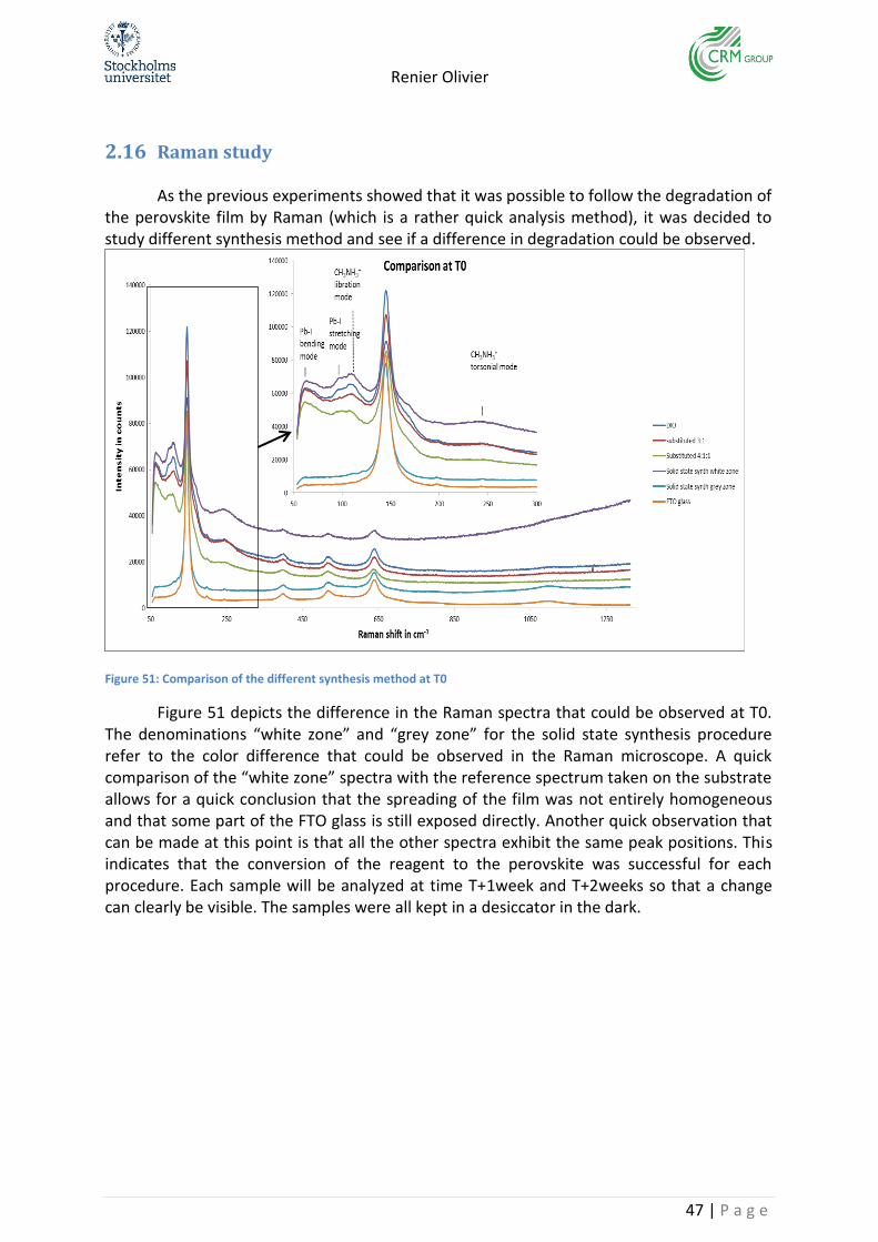
Renier Olivier
47 | P a g e
2.16 Raman study
As the previous experiments showed that it was possible to follow the degradation of the perovskite film by Raman (which is a rather quick analysis method), it was decided to study different synthesis method and see if a difference in degradation could be observed.
Figure 51: Comparison of the different synthesis method at T0
Figure 51 depicts the difference in the Raman spectra that could be observed at T0. The denominations “white zone” and “grey zone” for the solid state synthesis procedure refer to the color difference that could be observed in the Raman microscope. A quick comparison of the “white zone” spectra with the reference spectrum taken on the substrate allows for a quick conclusion that the spreading of the film was not entirely homogeneous and that some part of the FTO glass is still exposed directly. Another quick observation that can be made at this point is that all the other spectra exhibit the same peak positions. This indicates that the conversion of the reagent to the perovskite was successful for each procedure. Each sample will be analyzed at time T+1week and T+2weeks so that a change can clearly be visible. The samples were all kept in a desiccator in the dark.
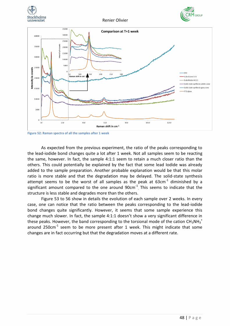
Renier Olivier
48 | P a g e
Figure 52: Raman spectra of all the samples after 1 week
As expected from the previous experiment, the ratio of the peaks corresponding to
the lead-iodide bond changes quite a lot after 1 week. Not all samples seem to be reacting the same, however. In fact, the sample 4:1:1 seem to retain a much closer ratio than the others. This could potentially be explained by the fact that some lead Iodide was already added to the sample preparation. Another probable explanation would be that this molar ratio is more stable and that the degradation may be delayed. The solid-state synthesis attempt seems to be the worst of all samples as the peak at 63cm-1 diminished by a significant amount compared to the one around 90cm-1
. This seems to indicate that the structure is less stable and degrades more than the others.
Figure 53 to 56 show in details the evolution of each sample over 2 weeks. In every case, one can notice that the ratio between the peaks corresponding to the lead-iodide bond changes quite significantly. However, it seems that some sample experience this change much slower. In fact, the sample 4:1:1 doesn’t show a very significant difference in these peaks. However, the band corresponding to the torsional mode of the cation CH3NH3
+ around 250cm-1 seem to be more present after 1 week. This might indicate that some changes are in fact occurring but that the degradation moves at a different rate.
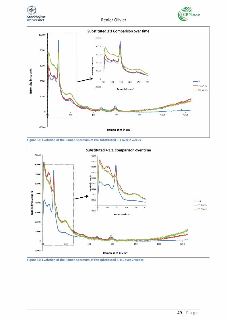
Renier Olivier
49 | P a g e
Figure 53: Evolution of the Raman spectrum of the substituted 3:1 over 2 weeks
Figure 54: Evolution of the Raman spectrum of the substituted 4:1:1 over 2 weeks
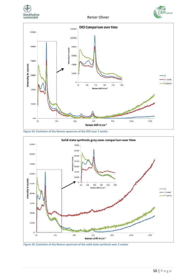
Renier Olivier
50 | P a g e
Figure 55: Evolution of the Raman spectrum of the DIO over 2 weeks
Figure 56: Evolution of the Raman spectrum of the solid-state synthesis over 2 weeks
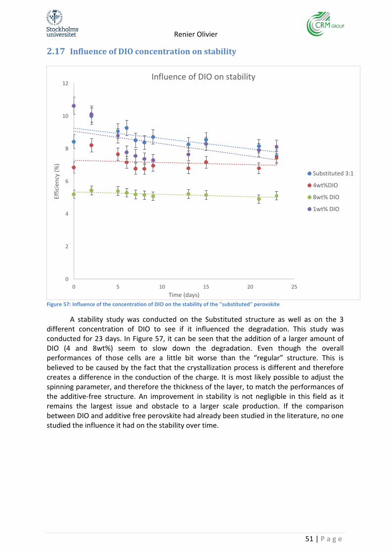
Renier Olivier
51 | P a g e
2.17 Influence of DIO concentration on stability
Figure 57: Influence of the concentration of DIO on the stability of the "substituted" perovskite
A stability study was conducted on the Substituted structure as well as on the 3 different concentration of DIO to see if it influenced the degradation. This study was conducted for 23 days. In Figure 57, it can be seen that the addition of a larger amount of DIO (4 and 8wt%) seem to slow down the degradation. Even though the overall performances of those cells are a little bit worse than the “regular” structure. This is believed to be caused by the fact that the crystallization process is different and therefore creates a difference in the conduction of the charge. It is most likely possible to adjust the spinning parameter, and therefore the thickness of the layer, to match the performances of the additive-free structure. An improvement in stability is not negligible in this field as it remains the largest issue and obstacle to a larger scale production. If the comparison between DIO and additive free perovskite had already been studied in the literature, no one studied the influence it had on the stability over time.
0
2
4
6
8
10
12
0 5 10 15 20 25
Effi
cien
cy (
%)
Time (days)
Influence of DIO on stability
Substituted 3:1
4wt%DIO
8wt% DIO
1wt% DIO
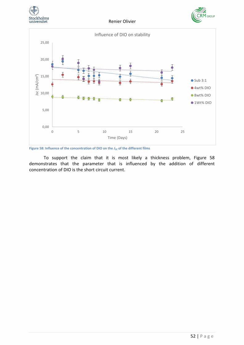
Renier Olivier
52 | P a g e
Figure 58: Influence of the concentration of DIO on the JSC of the different films
To support the claim that it is most likely a thickness problem, Figure 58 demonstrates that the parameter that is influenced by the addition of different concentration of DIO is the short circuit current.
0,00
5,00
10,00
15,00
20,00
25,00
0 5 10 15 20 25
Jsc
(mA
/cm
²)
Time (Days)
Influence of DIO on stability
Sub 3:1
4wt% DIO
8wt% DIO
1Wt% DIO
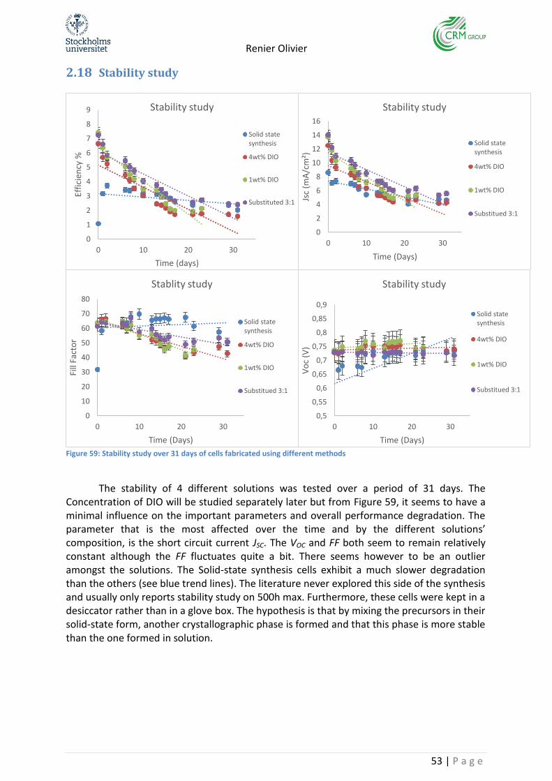
Renier Olivier
53 | P a g e
2.18 Stability study
Figure 59: Stability study over 31 days of cells fabricated using different methods
The stability of 4 different solutions was tested over a period of 31 days. The
Concentration of DIO will be studied separately later but from Figure 59, it seems to have a minimal influence on the important parameters and overall performance degradation. The parameter that is the most affected over the time and by the different solutions’ composition, is the short circuit current JSC. The VOC and FF both seem to remain relatively constant although the FF fluctuates quite a bit. There seems however to be an outlier amongst the solutions. The Solid-state synthesis cells exhibit a much slower degradation than the others (see blue trend lines). The literature never explored this side of the synthesis and usually only reports stability study on 500h max. Furthermore, these cells were kept in a desiccator rather than in a glove box. The hypothesis is that by mixing the precursors in their solid-state form, another crystallographic phase is formed and that this phase is more stable than the one formed in solution.
0,5
0,55
0,6
0,65
0,7
0,75
0,8
0,85
0,9
0 10 20 30
Vo
c (V
)
Time (Days)
Stability study
Solid statesynthesis
4wt% DIO
1wt% DIO
Substitued 3:1
0
2
4
6
8
10
12
14
16
0 10 20 30
Jsc
(mA
/cm
²)
Time (Days)
Stability study
Solid statesynthesis
4wt% DIO
1wt% DIO
Substitued 3:1
0
10
20
30
40
50
60
70
80
0 10 20 30
Fill
Fact
or
Time (Days)
Stablity study
Solid statesynthesis
4wt% DIO
1wt% DIO
Substitued 3:1
0
1
2
3
4
5
6
7
8
9
0 10 20 30
Effi
cien
cy %
Time (days)
Stability study
Solid statesynthesis
4wt% DIO
1wt% DIO
Substituted 3:1
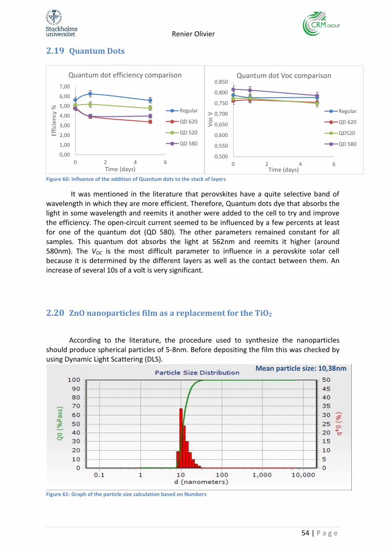
Renier Olivier
54 | P a g e
2.19 Quantum Dots
Figure 60: Influence of the addition of Quantum dots to the stack of layers
It was mentioned in the literature that perovskites have a quite selective band of wavelength in which they are more efficient. Therefore, Quantum dots dye that absorbs the light in some wavelength and reemits it another were added to the cell to try and improve the efficiency. The open-circuit current seemed to be influenced by a few percents at least for one of the quantum dot (QD 580). The other parameters remained constant for all samples. This quantum dot absorbs the light at 562nm and reemits it higher (around 580nm). The VOC is the most difficult parameter to influence in a perovskite solar cell because it is determined by the different layers as well as the contact between them. An increase of several 10s of a volt is very significant.
2.20 ZnO nanoparticles film as a replacement for the TiO2
According to the literature, the procedure used to synthesize the nanoparticles should produce spherical particles of 5-8nm. Before depositing the film this was checked by using Dynamic Light Scattering (DLS).
Figure 61: Graph of the particle size calculation based on Numbers
0,00
1,00
2,00
3,00
4,00
5,00
6,00
7,00
0 2 4 6
Effi
cien
cy %
Time (days)
Quantum dot efficiency comparison
Regular
QD 620
QD 520
QD 580
0,500
0,550
0,600
0,650
0,700
0,750
0,800
0,850
0 2 4 6
Vo
c V
Time (days)
Quantum dot Voc comparison
Regular
QD 620
QD520
QD 580
Mean particle size: 10,38nm
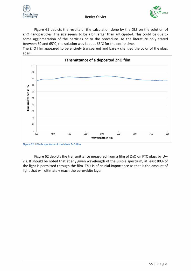
Renier Olivier
55 | P a g e
Figure 61 depicts the results of the calculation done by the DLS on the solution of
ZnO nanoparticles. The size seems to be a bit larger than anticipated. This could be due to some agglomeration of the particles or to the procedure. As the literature only stated between 60 and 65°C, the solution was kept at 65°C for the entire time. The ZnO film appeared to be entirely transparent and barely changed the color of the glass at all.
Figure 62: UV-vis spectrum of the blank ZnO film
Figure 62 depicts the transmittance measured from a film of ZnO on FTO glass by Uv-
vis. It should be noted that at any given wavelength of the visible spectrum, at least 80% of the light is permitted through the film. This is of crucial importance as that is the amount of light that will ultimately reach the perovskite layer.
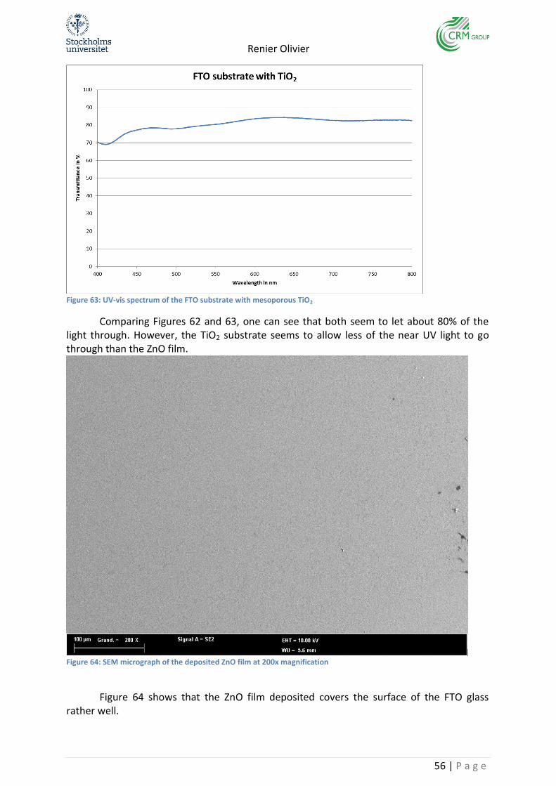
Renier Olivier
56 | P a g e
Figure 63: UV-vis spectrum of the FTO substrate with mesoporous TiO2
Comparing Figures 62 and 63, one can see that both seem to let about 80% of the light through. However, the TiO2 substrate seems to allow less of the near UV light to go through than the ZnO film.
Figure 64: SEM micrograph of the deposited ZnO film at 200x magnification
Figure 64 shows that the ZnO film deposited covers the surface of the FTO glass
rather well.
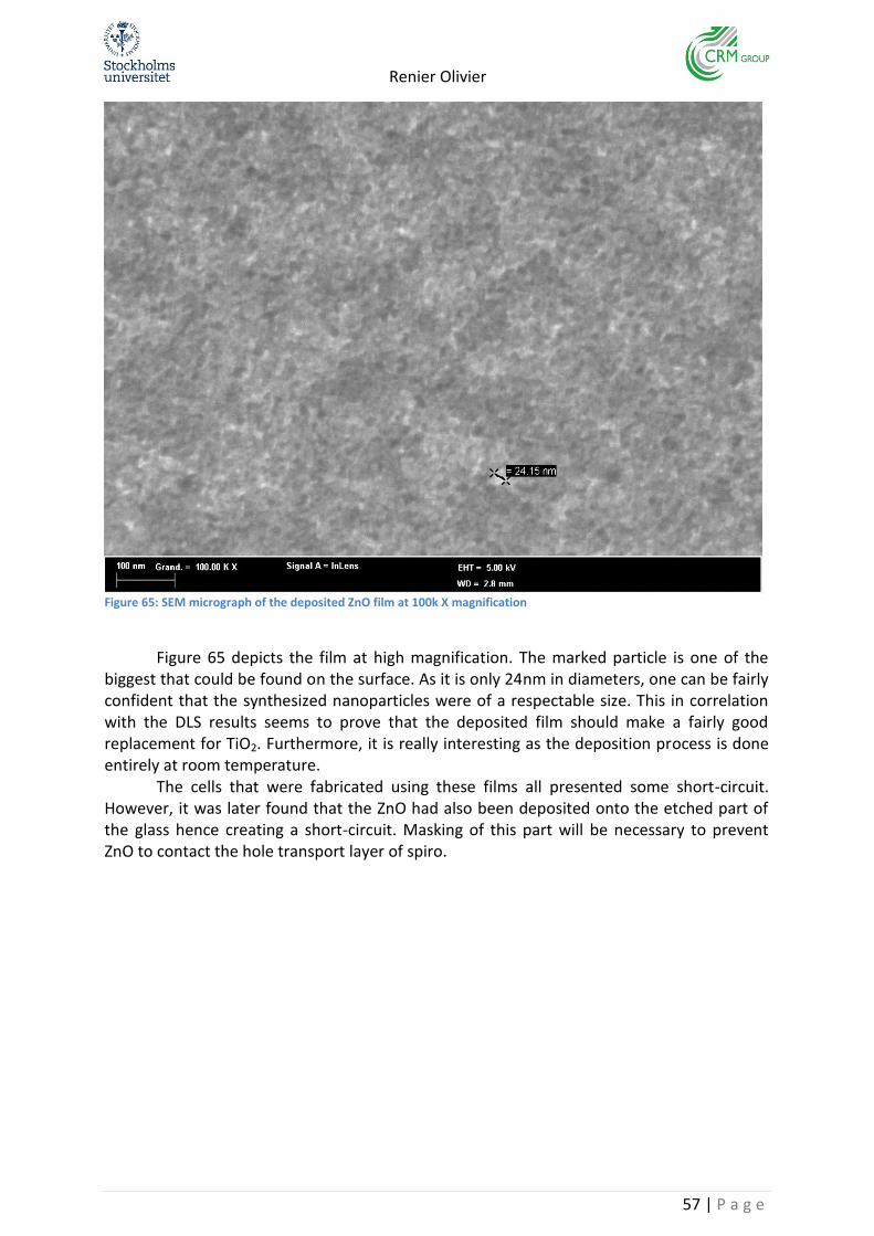
Renier Olivier
57 | P a g e
Figure 65: SEM micrograph of the deposited ZnO film at 100k X magnification
Figure 65 depicts the film at high magnification. The marked particle is one of the
biggest that could be found on the surface. As it is only 24nm in diameters, one can be fairly confident that the synthesized nanoparticles were of a respectable size. This in correlation with the DLS results seems to prove that the deposited film should make a fairly good replacement for TiO2. Furthermore, it is really interesting as the deposition process is done entirely at room temperature.
The cells that were fabricated using these films all presented some short-circuit. However, it was later found that the ZnO had also been deposited onto the etched part of the glass hence creating a short-circuit. Masking of this part will be necessary to prevent ZnO to contact the hole transport layer of spiro.
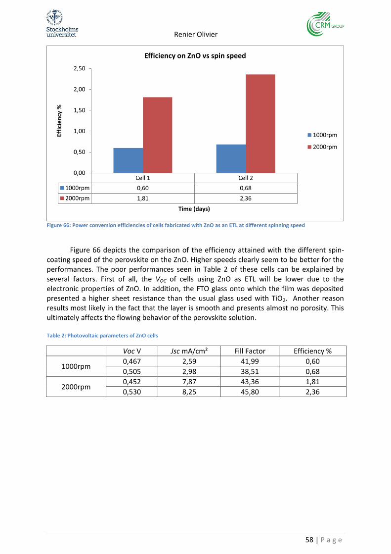
Renier Olivier
58 | P a g e
Figure 66: Power conversion efficiencies of cells fabricated with ZnO as an ETL at different spinning speed
Figure 66 depicts the comparison of the efficiency attained with the different spin-
coating speed of the perovskite on the ZnO. Higher speeds clearly seem to be better for the performances. The poor performances seen in Table 2 of these cells can be explained by several factors. First of all, the VOC of cells using ZnO as ETL will be lower due to the electronic properties of ZnO. In addition, the FTO glass onto which the film was deposited presented a higher sheet resistance than the usual glass used with TiO2. Another reason results most likely in the fact that the layer is smooth and presents almost no porosity. This ultimately affects the flowing behavior of the perovskite solution. Table 2: Photovoltaic parameters of ZnO cells
Voc V Jsc mA/cm² Fill Factor Efficiency %
1000rpm 0,467 2,59 41,99 0,60
0,505 2,98 38,51 0,68
2000rpm 0,452 7,87 43,36 1,81
0,530 8,25 45,80 2,36
Cell 1 Cell 2
1000rpm 0,60 0,68
2000rpm 1,81 2,36
0,00
0,50
1,00
1,50
2,00
2,50
Effi
cie
ncy
%
Time (days)
Efficiency on ZnO vs spin speed
1000rpm
2000rpm
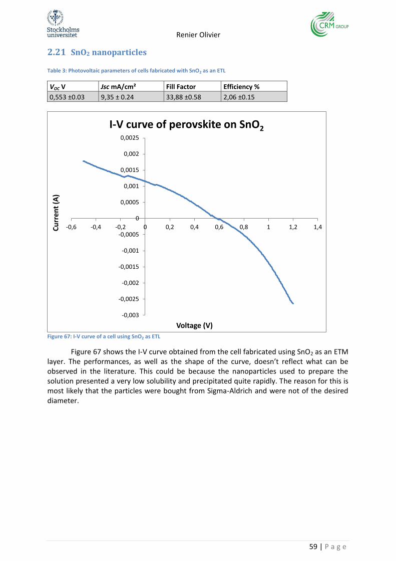
Renier Olivier
59 | P a g e
2.21 SnO2 nanoparticles Table 3: Photovoltaic parameters of cells fabricated with SnO2 as an ETL
VOC V Jsc mA/cm² Fill Factor Efficiency %
0,553 ±0.03 9,35 ± 0.24 33,88 ±0.58 2,06 ±0.15
Figure 67: I-V curve of a cell using SnO2 as ETL
Figure 67 shows the I-V curve obtained from the cell fabricated using SnO2 as an ETM layer. The performances, as well as the shape of the curve, doesn’t reflect what can be observed in the literature. This could be because the nanoparticles used to prepare the solution presented a very low solubility and precipitated quite rapidly. The reason for this is most likely that the particles were bought from Sigma-Aldrich and were not of the desired diameter.
-0,003
-0,0025
-0,002
-0,0015
-0,001
-0,0005
0
0,0005
0,001
0,0015
0,002
0,0025
-0,6 -0,4 -0,2 0 0,2 0,4 0,6 0,8 1 1,2 1,4Cu
rren
t (A
)
Voltage (V)
I-V curve of perovskite on SnO2
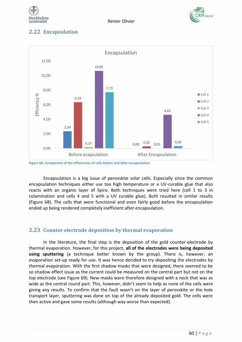
Renier Olivier
60 | P a g e
2.22 Encapsulation
Figure 68: Comparison of the efficiencies of cells before and after encapsulation
Encapsulation is a big issue of perovskite solar cells. Especially since the common
encapsulation techniques either use too high temperature or a UV-curable glue that also reacts with an organic layer of Spiro. Both techniques were tried here (cell 1 to 3 in colamination and cells 4 and 5 with a UV curable glue). Both resulted in similar results (Figure 68). The cells that were functional and even fairly good before the encapsulation ended up being rendered completely inefficient after encapsulation.
2.23 Counter electrode deposition by thermal evaporation
In the literature, the final step is the deposition of the gold counter-electrode by thermal evaporation. However, for this project, all of the electrodes were being deposited using sputtering (a technique better known by the group). There is, however, an evaporation set-up ready for use. It was hence decided to try depositing the electrodes by thermal evaporation. With the first shadow masks that were designed, there seemed to be so shadow effect issue as the current could be measured on the central part but not on the top electrode (see Figure 69). New masks were therefore designed with a neck that was as wide as the central round part. This, however, didn’t seem to help as none of the cells were giving any results. To confirm that the fault wasn’t on the layer of perovskite or the hole transport layer, sputtering was done on top of the already deposited gold. The cells were then active and gave some results (although way worse than expected).
2,34
0,00
6,34
0,26 0,15 0,01
10,65
4,62
7,73
0,30
0,00
2,00
4,00
6,00
8,00
10,00
12,00
Before ecapsulation After Encapsulation
Effi
cien
cy %
Encapsulation
Cell 1
Cell 2
Cell 3
Cell 4
Cell 5
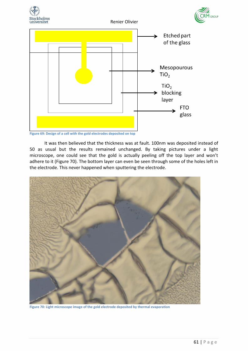
Renier Olivier
61 | P a g e
Figure 69: Design of a cell with the gold electrodes deposited on top
It was then believed that the thickness was at fault. 100nm was deposited instead of 50 as usual but the results remained unchanged. By taking pictures under a light microscope, one could see that the gold is actually peeling off the top layer and won’t adhere to it (Figure 70). The bottom layer can even be seen through some of the holes left in the electrode. This never happened when sputtering the electrode.
Figure 70: Light microscope image of the gold electrode deposited by thermal evaporation
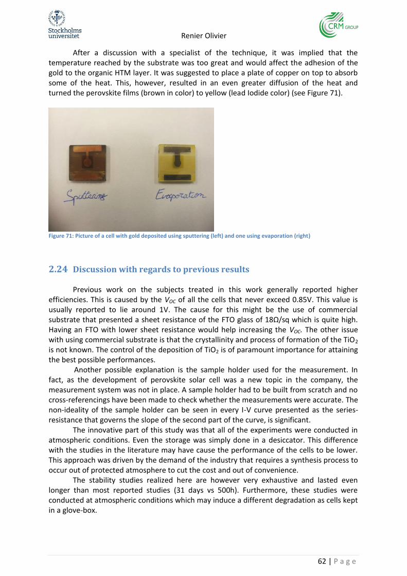
Renier Olivier
62 | P a g e
After a discussion with a specialist of the technique, it was implied that the temperature reached by the substrate was too great and would affect the adhesion of the gold to the organic HTM layer. It was suggested to place a plate of copper on top to absorb some of the heat. This, however, resulted in an even greater diffusion of the heat and turned the perovskite films (brown in color) to yellow (lead Iodide color) (see Figure 71).
Figure 71: Picture of a cell with gold deposited using sputtering (left) and one using evaporation (right)
2.24 Discussion with regards to previous results
Previous work on the subjects treated in this work generally reported higher efficiencies. This is caused by the VOC of all the cells that never exceed 0.85V. This value is usually reported to lie around 1V. The cause for this might be the use of commercial substrate that presented a sheet resistance of the FTO glass of 18Ω/sq which is quite high. Having an FTO with lower sheet resistance would help increasing the VOC. The other issue with using commercial substrate is that the crystallinity and process of formation of the TiO2 is not known. The control of the deposition of TiO2 is of paramount importance for attaining the best possible performances.
Another possible explanation is the sample holder used for the measurement. In fact, as the development of perovskite solar cell was a new topic in the company, the measurement system was not in place. A sample holder had to be built from scratch and no cross-referencings have been made to check whether the measurements were accurate. The non-ideality of the sample holder can be seen in every I-V curve presented as the series-resistance that governs the slope of the second part of the curve, is significant.
The innovative part of this study was that all of the experiments were conducted in atmospheric conditions. Even the storage was simply done in a desiccator. This difference with the studies in the literature may have cause the performance of the cells to be lower. This approach was driven by the demand of the industry that requires a synthesis process to occur out of protected atmosphere to cut the cost and out of convenience.
The stability studies realized here are however very exhaustive and lasted even longer than most reported studies (31 days vs 500h). Furthermore, these studies were conducted at atmospheric conditions which may induce a different degradation as cells kept in a glove-box.
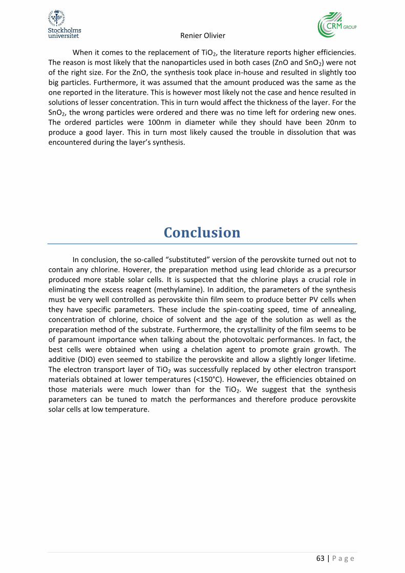
Renier Olivier
63 | P a g e
When it comes to the replacement of TiO2, the literature reports higher efficiencies. The reason is most likely that the nanoparticles used in both cases (ZnO and SnO2) were not of the right size. For the ZnO, the synthesis took place in-house and resulted in slightly too big particles. Furthermore, it was assumed that the amount produced was the same as the one reported in the literature. This is however most likely not the case and hence resulted in solutions of lesser concentration. This in turn would affect the thickness of the layer. For the SnO2, the wrong particles were ordered and there was no time left for ordering new ones. The ordered particles were 100nm in diameter while they should have been 20nm to produce a good layer. This in turn most likely caused the trouble in dissolution that was encountered during the layer’s synthesis.
Conclusion
In conclusion, the so-called “substituted” version of the perovskite turned out not to contain any chlorine. Hoverer, the preparation method using lead chloride as a precursor produced more stable solar cells. It is suspected that the chlorine plays a crucial role in eliminating the excess reagent (methylamine). In addition, the parameters of the synthesis must be very well controlled as perovskite thin film seem to produce better PV cells when they have specific parameters. These include the spin-coating speed, time of annealing, concentration of chlorine, choice of solvent and the age of the solution as well as the preparation method of the substrate. Furthermore, the crystallinity of the film seems to be of paramount importance when talking about the photovoltaic performances. In fact, the best cells were obtained when using a chelation agent to promote grain growth. The additive (DIO) even seemed to stabilize the perovskite and allow a slightly longer lifetime. The electron transport layer of TiO2 was successfully replaced by other electron transport materials obtained at lower temperatures (<150°C). However, the efficiencies obtained on those materials were much lower than for the TiO2. We suggest that the synthesis parameters can be tuned to match the performances and therefore produce perovskite solar cells at low temperature.

Renier Olivier
64 | P a g e
Future prospects
The first advice that could be given for improving the quality of the research in this topic would be to test the sample holder and compare it to a system that is known to produce reliable results. The device should be built to be a little bit more durable as well. As the development of perovskite solar cells is just at its beginning in the CRM group, the possibilities for improvements are numerous.
As for the project, the recommendations for continuing include the exploration of combination of recrystallization methods to try and improve the efficiency further. Another point would be to keep studying the effects of the DIO on the stability, especially at higher concentrations and try to adjust the synthesis parameters (spin-coating speed, concentration of the solution, annealing time…) to obtain the desired efficiencies. As previously stated, the parameters should also be tuned for the perovskite deposited on the alternative ETL (ZnO and SnO2). With regards to this point, the experiments should be repeated with different size of nanoparticles to see its influence on the performances. Raman should be used more to study both the degradation of the perovskite film, but on a shorter time scale (every day instead of once a week), and the kinetics of the solution. The solid state synthesis procedure should also be investigated further to understand why the certain parameters were so much higher and why this solution exhibited a higher stability.
Finally, the system should be adapted to be able to move towards flexible or metallic substrates. To do so, we suggest investigating the solutions for dispensing TiO2 at lower temperature (although this might prove difficult as most solutions are aqueous) as well as to try and transfer the optimized version of the ZnO or SnO2 procedure. This could allow starting some try-outs on larger scale using the roll-to-roll process that can be implemented onto pilot lines.
Acknowledgments
I would like to extend my thanks towards Adeline Lafort for her supervision during the whole project and all the great discussion we had. I would also like to thanks Prof. Gunnar Svensson for his supervision from Stockholm. I would like to thanks Lionel Fourdrinier for his expertise and advice in the photovoltaic field. Kevin Barbette for the deposition of the gold electrodes by sputtering, Christophe Kempeneers for his help building different sample holders, Philippe Bourguignon for his help with pretty much any problem encountered. Finally, I would like to thank the CRM group and more particularly the AC&CS team for welcoming me into their research group as well as the department of MMK for allowing me to conduct my thesis abroad in this company.
Renier Olivier
65 | P a g e
References
[1] R. Fang, W. Zhang, S. Zhang, and W. Chen, “The rising star in photovoltaics-perovskite
solar cells: The past, present and future,” Sci. China Technol. Sci., no. 7, 989–1006, 2016.
[2] B. R. Sutherland, “Tailoring Perovskite Thin Films to Rival Single Crystals,” Joule, vol. 1, no. 1, pp. 23–25, 2017.
[3] D. W. deQuilettes et al., “Photo-induced halide redistribution in organic–inorganic perovskite films,” Nat. Commun., vol. 7, p. 11683, May 2016.
[4] M. Saliba et al., “Structured organic–inorganic perovskite toward a distributed feedback laser,” Adv. Mater., vol. 28, no. 5, pp. 923–929, 2016.
[5] X. Y. Chin, D. Cortecchia, J. Yin, A. Bruno, and C. Soci, “Lead iodide perovskite light-emitting field-effect transistor,” Nat. Commun., vol. 6, p. 7383, 2015.
[6] A. Kojima, K. Teshima, Y. Shirai, and T. Miyasaka, “Organometal halide perovskites as visible-light sensitizers for photovoltaic cells,” J. Am. Chem. Soc., vol. 131, no. 17, pp. 6050–6051, 2009.
[7] W. S. Yang et al., “High-performance photovoltaic perovskite layers fabricated through intramolecular exchange,” Science, vol. 348, no. 6240, pp. 1234–1237, 2015.
[8] J. S. Manser, J. A. Christians, and P. V. Kamat, “Intriguing Optoelectronic Properties of Metal Halide Perovskites,” Chem. Rev., vol. 116, no. 21, pp. 12956–13008, Nov. 2016.
[9] R. Perez and M. Perez, “A fundamental look at energy reserves for the planet,” IEA SHC Sol. Update, vol. 50, no. 2, 2009.
[10] B. Parida, S. Iniyan, and R. Goic, “A review of solar photovoltaic technologies,” Renew. Sustain. Energy Rev., vol. 15, no. 3, pp. 1625–1636, Apr. 2011.
[11] C. A. Ubani, M. A. Ibrahim, and M. A. M. Teridi, “Moving into the domain of perovskite sensitized solar cell,” Renew. Sustain. Energy Rev., vol. 72, pp. 907–915, May 2017.
[12] M. M. Lee, J. Teuscher, T. Miyasaka, T. N. Murakami, and H. J. Snaith, “Efficient hybrid solar cells based on meso-superstructured organometal halide perovskites,” Science, p. 1228604, 2012.
[13] J. Gong, K. Sumathy, Q. Qiao, and Z. Zhou, “Review on dye-sensitized solar cells (DSSCs): Advanced techniques and research trends,” Renew. Sustain. Energy Rev., vol. 68, pp. 234–246, Feb. 2017.
[14] F. M. González-Longatt, “Model of photovoltaic module in Matlab,” Ii Cibelec, vol. 2005, pp. 1–5, 2005.
[15] P. Gao, M. Grätzel, and M. K. Nazeeruddin, “Organohalide lead perovskites for photovoltaic applications,” Energy Environ. Sci., vol. 7, no. 8, pp. 2448–2463, 2014.
[16] T. Baikie et al., “Synthesis and crystal chemistry of the hybrid perovskite (CH 3 NH 3) PbI 3 for solid-state sensitised solar cell applications,” J. Mater. Chem. A, vol. 1, no. 18, pp. 5628–5641, 2013.
[17] M. D. Bhatt and J. S. Lee, “Current progress and scientific challenges in the advancement of organic–inorganic lead halide perovskite solar cells,” New J. Chem., vol. 41, no. 19, pp. 10508–10527, 2017.
[18] M. A. Green, A. Ho-Baillie, and H. J. Snaith, “The emergence of perovskite solar cells,” Nat. Photonics, vol. 8, p. 506, Jun. 2014.
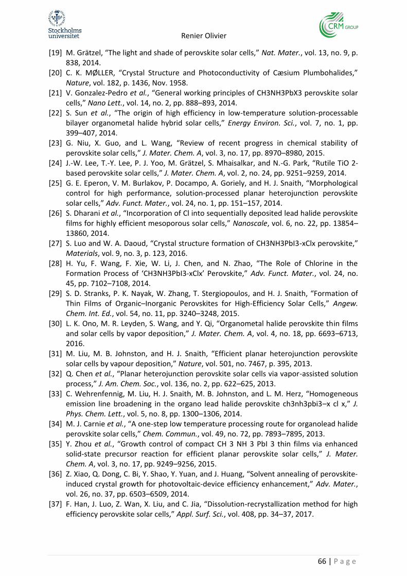
Renier Olivier
66 | P a g e
[19] M. Grätzel, “The light and shade of perovskite solar cells,” Nat. Mater., vol. 13, no. 9, p. 838, 2014.
[20] C. K. MØLLER, “Crystal Structure and Photoconductivity of Cæsium Plumbohalides,” Nature, vol. 182, p. 1436, Nov. 1958.
[21] V. Gonzalez-Pedro et al., “General working principles of CH3NH3PbX3 perovskite solar cells,” Nano Lett., vol. 14, no. 2, pp. 888–893, 2014.
[22] S. Sun et al., “The origin of high efficiency in low-temperature solution-processable bilayer organometal halide hybrid solar cells,” Energy Environ. Sci., vol. 7, no. 1, pp. 399–407, 2014.
[23] G. Niu, X. Guo, and L. Wang, “Review of recent progress in chemical stability of perovskite solar cells,” J. Mater. Chem. A, vol. 3, no. 17, pp. 8970–8980, 2015.
[24] J.-W. Lee, T.-Y. Lee, P. J. Yoo, M. Grätzel, S. Mhaisalkar, and N.-G. Park, “Rutile TiO 2-based perovskite solar cells,” J. Mater. Chem. A, vol. 2, no. 24, pp. 9251–9259, 2014.
[25] G. E. Eperon, V. M. Burlakov, P. Docampo, A. Goriely, and H. J. Snaith, “Morphological control for high performance, solution‐processed planar heterojunction perovskite solar cells,” Adv. Funct. Mater., vol. 24, no. 1, pp. 151–157, 2014.
[26] S. Dharani et al., “Incorporation of Cl into sequentially deposited lead halide perovskite films for highly efficient mesoporous solar cells,” Nanoscale, vol. 6, no. 22, pp. 13854–13860, 2014.
[27] S. Luo and W. A. Daoud, “Crystal structure formation of CH3NH3PbI3-xClx perovskite,” Materials, vol. 9, no. 3, p. 123, 2016.
[28] H. Yu, F. Wang, F. Xie, W. Li, J. Chen, and N. Zhao, “The Role of Chlorine in the Formation Process of ‘CH3NH3PbI3‐xClx’ Perovskite,” Adv. Funct. Mater., vol. 24, no. 45, pp. 7102–7108, 2014.
[29] S. D. Stranks, P. K. Nayak, W. Zhang, T. Stergiopoulos, and H. J. Snaith, “Formation of Thin Films of Organic–Inorganic Perovskites for High‐Efficiency Solar Cells,” Angew. Chem. Int. Ed., vol. 54, no. 11, pp. 3240–3248, 2015.
[30] L. K. Ono, M. R. Leyden, S. Wang, and Y. Qi, “Organometal halide perovskite thin films and solar cells by vapor deposition,” J. Mater. Chem. A, vol. 4, no. 18, pp. 6693–6713, 2016.
[31] M. Liu, M. B. Johnston, and H. J. Snaith, “Efficient planar heterojunction perovskite solar cells by vapour deposition,” Nature, vol. 501, no. 7467, p. 395, 2013.
[32] Q. Chen et al., “Planar heterojunction perovskite solar cells via vapor-assisted solution process,” J. Am. Chem. Soc., vol. 136, no. 2, pp. 622–625, 2013.
[33] C. Wehrenfennig, M. Liu, H. J. Snaith, M. B. Johnston, and L. M. Herz, “Homogeneous emission line broadening in the organo lead halide perovskite ch3nh3pbi3–x cl x,” J. Phys. Chem. Lett., vol. 5, no. 8, pp. 1300–1306, 2014.
[34] M. J. Carnie et al., “A one-step low temperature processing route for organolead halide perovskite solar cells,” Chem. Commun., vol. 49, no. 72, pp. 7893–7895, 2013.
[35] Y. Zhou et al., “Growth control of compact CH 3 NH 3 PbI 3 thin films via enhanced solid-state precursor reaction for efficient planar perovskite solar cells,” J. Mater. Chem. A, vol. 3, no. 17, pp. 9249–9256, 2015.
[36] Z. Xiao, Q. Dong, C. Bi, Y. Shao, Y. Yuan, and J. Huang, “Solvent annealing of perovskite‐induced crystal growth for photovoltaic‐device efficiency enhancement,” Adv. Mater., vol. 26, no. 37, pp. 6503–6509, 2014.
[37] F. Han, J. Luo, Z. Wan, X. Liu, and C. Jia, “Dissolution-recrystallization method for high efficiency perovskite solar cells,” Appl. Surf. Sci., vol. 408, pp. 34–37, 2017.
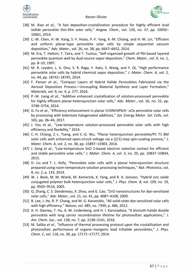
Renier Olivier
67 | P a g e
[38] M. Xiao et al., “A fast deposition‐crystallization procedure for highly efficient lead iodide perovskite thin‐film solar cells,” Angew. Chem., vol. 126, no. 37, pp. 10056–10061, 2014.
[39] C.-W. Chen, H.-W. Kang, S.-Y. Hsiao, P.-F. Yang, K.-M. Chiang, and H.-W. Lin, “Efficient and uniform planar‐type perovskite solar cells by simple sequential vacuum deposition,” Adv. Mater., vol. 26, no. 38, pp. 6647–6652, 2014.
[40] M. Era, T. Hattori, T. Taira, and T. Tsutsui, “Self-organized growth of PbI-based layered perovskite quantum well by dual-source vapor deposition,” Chem. Mater., vol. 9, no. 1, pp. 8–10, 1997.
[41] M. R. Leyden, L. K. Ono, S. R. Raga, Y. Kato, S. Wang, and Y. Qi, “High performance perovskite solar cells by hybrid chemical vapor deposition,” J. Mater. Chem. A, vol. 2, no. 44, pp. 18742–18745, 2014.
[42] F. Panzer et al., “Compact Layers of Hybrid Halide Perovskites Fabricated via the Aerosol Deposition Process—Uncoupling Material Synthesis and Layer Formation,” Materials, vol. 9, no. 4, p. 277, 2016.
[43] P.-W. Liang et al., “Additive enhanced crystallization of solution‐processed perovskite for highly efficient planar‐heterojunction solar cells,” Adv. Mater., vol. 26, no. 22, pp. 3748–3754, 2014.
[44] G. Fu et al., “Efficiency enhancement in planar CH3NH3PbI3− xClx perovskite solar cells by processing with bidentate halogenated additives,” Sol. Energy Mater. Sol. Cells, vol. 165, pp. 36–44, 2017.
[45] J. You et al., “Low-temperature solution-processed perovskite solar cells with high efficiency and flexibility,” 2014.
[46] C.-H. Chiang, Z.-L. Tseng, and C.-G. Wu, “Planar heterojunction perovskite/PC 71 BM solar cells with enhanced open-circuit voltage via a (2/1)-step spin-coating process,” J. Mater. Chem. A, vol. 2, no. 38, pp. 15897–15903, 2014.
[47] J. Song et al., “Low-temperature SnO 2-based electron selective contact for efficient and stable perovskite solar cells,” J. Mater. Chem. A, vol. 3, no. 20, pp. 10837–10844, 2015.
[48] D. Liu and T. L. Kelly, “Perovskite solar cells with a planar heterojunction structure prepared using room-temperature solution processing techniques,” Nat. Photonics, vol. 8, no. 2, p. 133, 2014.
[49] W. J. Beek, M. M. Wienk, M. Kemerink, X. Yang, and R. A. Janssen, “Hybrid zinc oxide conjugated polymer bulk heterojunction solar cells,” J. Phys. Chem. B, vol. 109, no. 19, pp. 9505–9516, 2005.
[50] Q. Zhang, C. S. Dandeneau, X. Zhou, and G. Cao, “ZnO nanostructures for dye‐sensitized solar cells,” Adv. Mater., vol. 21, no. 41, pp. 4087–4108, 2009.
[51] B. Lee, J. He, R. P. Chang, and M. G. Kanatzidis, “All-solid-state dye-sensitized solar cells with high efficiency,” Nature, vol. 485, no. 7399, p. 486, 2012.
[52] A. H. Slavney, T. Hu, A. M. Lindenberg, and H. I. Karunadasa, “A bismuth-halide double perovskite with long carrier recombination lifetime for photovoltaic applications,” J. Am. Chem. Soc., vol. 138, no. 7, pp. 2138–2141, 2016.
[53] M. Saliba et al., “Influence of thermal processing protocol upon the crystallization and photovoltaic performance of organic–inorganic lead trihalide perovskites,” J. Phys. Chem. C, vol. 118, no. 30, pp. 17171–17177, 2014.
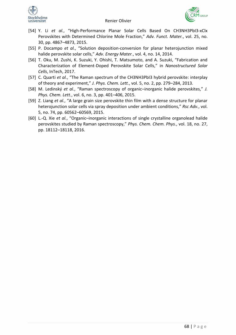
Renier Olivier
68 | P a g e
[54] Y. Li et al., “High‐Performance Planar Solar Cells Based On CH3NH3PbI3‐xClx Perovskites with Determined Chlorine Mole Fraction,” Adv. Funct. Mater., vol. 25, no. 30, pp. 4867–4873, 2015.
[55] P. Docampo et al., “Solution deposition‐conversion for planar heterojunction mixed halide perovskite solar cells,” Adv. Energy Mater., vol. 4, no. 14, 2014.
[56] T. Oku, M. Zushi, K. Suzuki, Y. Ohishi, T. Matsumoto, and A. Suzuki, “Fabrication and Characterization of Element-Doped Perovskite Solar Cells,” in Nanostructured Solar Cells, InTech, 2017.
[57] C. Quarti et al., “The Raman spectrum of the CH3NH3PbI3 hybrid perovskite: interplay of theory and experiment,” J. Phys. Chem. Lett., vol. 5, no. 2, pp. 279–284, 2013.
[58] M. Ledinský et al., “Raman spectroscopy of organic–inorganic halide perovskites,” J. Phys. Chem. Lett., vol. 6, no. 3, pp. 401–406, 2015.
[59] Z. Liang et al., “A large grain size perovskite thin film with a dense structure for planar heterojunction solar cells via spray deposition under ambient conditions,” Rsc Adv., vol. 5, no. 74, pp. 60562–60569, 2015.
[60] L.-Q. Xie et al., “Organic–inorganic interactions of single crystalline organolead halide perovskites studied by Raman spectroscopy,” Phys. Chem. Chem. Phys., vol. 18, no. 27, pp. 18112–18118, 2016.