Embed Size (px)
Citation preview
International Journal of NanoScience and Nanotechnology. ISSN 0974-3081 Volume 6, Number 1 (2015), pp. 57-70
© International Research Publication House
http://www.irphouse.com
Development Of Large Area Nanostructured
Antireflection Coatings For EO/IR Sensor
Applications
Ashok K. Sood, Gopal Pethuraja, Roger E. Welser and Yash R. Puri
Magnolia Optical Technologies, Inc. 52-B Cummings Park, Suite 314, Woburn, MA
Nibir K. Dhar
Night Vision & Electronic Sensors Directorate,
10221 Burbeck Road Fort Belvoir, Virginia 22060
Priyalal S. Wijewarnasuriya
Army Research Laboratory, 2800 Powder Mill Road, Adelphi, MD 20783
Jay Lewis
DARPA/MTO, 675 North Randolph Street, Arlington, VA 22203
Harry Efstathiadis and Pradeep Haldar
College of Nanoscale Science and Engineering (CNSE), Albany, NY 12222
E. Fred Schubert
Department of ECSE and Physics, Rensselaer Polytechnic Institute, Troy, NY 12180
ABSTRACT
Electro-optical/infrared nanosensors are being developed for a variety of
defense and commercial systems applications. One of the critical technologies that will enhance EO/IR sensor performance is the development of advanced
antireflection coatings with both broadband and omnidirectional
characteristics.In this paper, we review our latest work on high quality
nanostructure-based antireflection structures, including recent efforts to deposit nanostructured antireflection coatings on large area substrates.

58 Ashok K. Sood et al
Nanostructured antireflection coatingsfabricated via oblique angle deposition are shown to enhance the optical transmission through transparent windows
by minimizing broadband reflection losses to less than one percent, a
substantial improvement over conventional thin-film antireflection coating technologies. Step-graded antireflection structures also exhibit excellent
omnidirectional performance, and have recently been demonstrated on 6-inch
diameter substrates.
INTRODUCTION
Electro-optical/infrared (EO/IR) nanosensors are being developed for a variety of
defense and commercial systems applications [1-10]. These include ultraviolet (UV), visible, near infrared (NIR), mid-wavelength infrared (MWIR), and long-wavelength
infrared (LWIR) nanotechnology-based sensors. All of these EO/IR nanosensor
technologies will benefit from the development of advanced antireflection
(AR)coatings that minimize reflection losses over a wide range of wavelengths and incident angles.
Theoretically, it has been known for some time that Fresnel reflection losses
can be minimized between two media by grading the refractive index across the
interface. However, the unavailability of materials with the desired refractive indices, particularly materials with very low refractive indices, has prevented the
implementation of graded and step-graded refractive index designs. Recently,
however, a new class of optical thin-film materials consisting of porous nanorods has
enabled the realization of ultra-low refractive index materials [11-13]. Oblique-angle deposition has been used to tailor the refractive index of
porous, nanostructured SiO2 materials, and to build high-performance step-graded
refractive index structures on glass and other relevant substrates. Step-grade designs
enable the formation of antireflection structures that combine broadband and omnidirectional characteristics. In this work, we review the oblique angle deposition
process,summarizerecent results from step-graded antireflection coatings on glass,
and discuss our efforts to extend the nanostructured coating process to larger area
substrates.
OBLIQUE ANGLE DEPOSITION
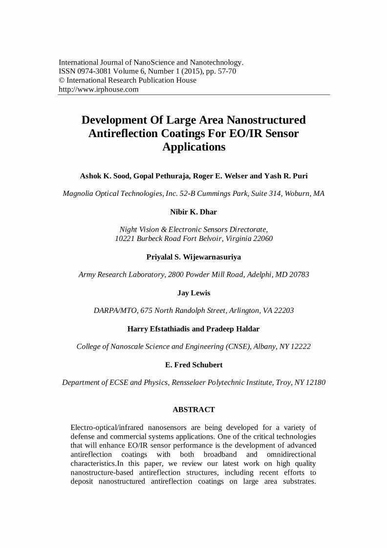
Figure 1 presents a detailed layout of the experimental setup of the oblique angle deposition technique for growth of porous nanostructured materials by e-beam
evaporation. This technique creates a highly directional vapor flux and can be
implemented with a variety of optical coating materials. Oblique-angle deposition is a
method of growing porous thin-films, and hence thin-films with low-refractive index, enabled by surface diffusion and self-shadowing effects during the deposition process.
Random growth fluctuations on the substrate produce a shadow region that incident
vapor flux cannot reach, and a non-shadow region where incident flux deposits
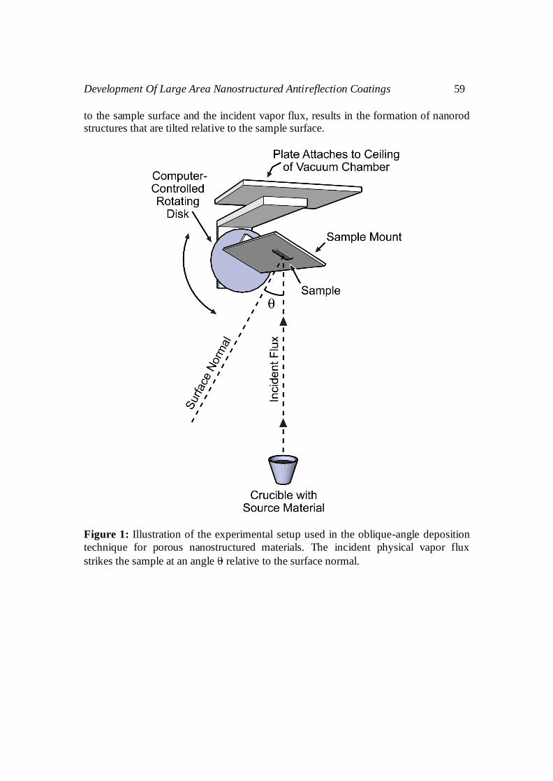
preferentially, thereby creating an oriented rod-like structure with high porosity, as illustrated in Figure 2. The deposition angle, defined as the angle between the normal
Development Of Large Area Nanostructured Antireflection Coatings 59
to the sample surface and the incident vapor flux, results in the formation of nanorod structures that are tilted relative to the sample surface.
Figure 1: Illustration of the experimental setup used in the oblique-angle deposition
technique for porous nanostructured materials. The incident physical vapor flux
strikes the sample at an angle relative to the surface normal.
60 Ashok K. Sood et al
Figure 2: (a) Simplified schematic of the oblique-angle deposition process for synthesizing porous, nanostructured films, showing (a) the initial formation of
material islands at random locations across the substrate, followed by (b) the
formation of self-shadowed regions and nano-columnar growth when material vapor
flux arrives at a non-normal deposition angle ( ) to the substrate.
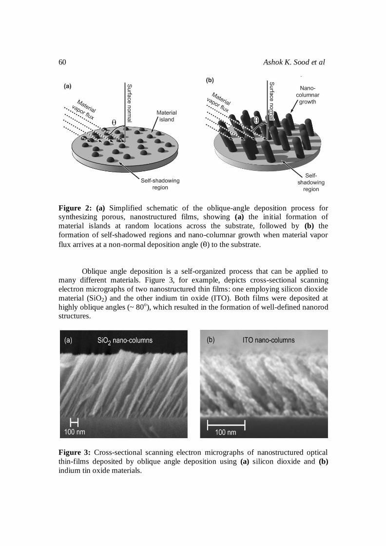
Oblique angle deposition is a self-organized process that can be applied to many different materials. Figure 3, for example, depicts cross-sectional scanning
electron micrographs of two nanostructured thin films: one employing silicon dioxide
material (SiO2) and the other indium tin oxide (ITO). Both films were deposited at
highly oblique angles (~ 80o), which resulted in the formation of well-defined nanorod structures.
Figure 3: Cross-sectional scanning electron micrographs of nanostructured optical
thin-films deposited by oblique angle deposition using (a) silicon dioxide and (b)
indium tin oxide materials.

Development Of Large Area Nanostructured Antireflection Coatings 61
Because the gaps between the nanorods can be much smaller than the wavelength of visible and infrared light, the nanostructured layers typically act as a
single homogenous film with a refractive index intermediate between air and the
nanorod material, decreasing in refractive index with increasing porosity. Figure 4 presents the measured refractive index dispersion curve as a function of wavelength
from a layer of nanostructured SiO2 deposited at a highly oblique angle [12]. This
low-index nanostructured SiO2 film was deposited on a silicon substrate and
measured by ellipsometry. Also shown is a comparison of experimental reflectivity data with theoretical calculations. These results illustrate that nanowires and nanorods
grown by the oblique angle deposition technique provide a pathway for fabricating
high-quality broadband anti-reflection coatings for a variety of nanosensor
applications.
Figure 4: (a) Refractive index dispersion curve of a low-index SiO2 nanorod thin film
on a silicon substrate as measured by ellipsometry, with (b) a comparison of the
measured and calculated reflectivity spectrum.
Figures 5 and 6 demonstrate the use of SiO2 and TiO2 nanowire and nanorods
to achieve a high-performance step-graded antireflection coating on an AlN substrate.
The feasibility of this technology has been demonstrated for UV light-emitting diode (LED) applications [12]. In the next section, we summarize our recent efforts to
extend this technology to other substrates and other bands of interest in the visible,
NIR, and MWIR spectrums for next-generation EO/IR sensors.
(b)

62 Ashok K. Sood et al
Figure 5: (a) Cross-sectional scanning electron micrograph of a TiO2 and SiO2 step-
graded index nanowire/nanorod coating which approximates a modified-quintic
profile. The graded-index coating consists of three TiO2 nanorod layers and two SiO2 nanorod layers. (b) The physical targets for each layer in the graded index coating,
including deposition angle, thickness and refractive index.
Figure 6: Reflectivity of the graded-index coating on an AlN substrate summarized
above in Figure 5, including (a) Schematic of the reflectivity measurement; (b)
Theoretical (solid line) and measured (dotted line) reflectivity of polarized light
versus incident angle; and (c) Wavelength dependence of theoretical (solid line) and measured (dashed line) reflectivity at normal incidence. Further details can be found
in reference [10].
(b)
Layer No. 1 2 3 4 5
Source TiO2 SiO2
Deposition
angle 25 40 65 –68 –87
Thickness
(nm) 77.4 80.2 99.3 145.0 223.0
Refractive
index, n 2.03 1.97 1.67 1.27 1.05
Development Of Large Area Nanostructured Antireflection Coatings 63
NANOSTRUCTURED ANTIREFLECTION COATINGS ON GLASS We have fabricated and tested a number of different step-graded antireflection
structures on glass substrates [14-16]. In particular, oblique angle deposition has been
used to deposit both two-and three-layer structures comprised of nanostructured SiO2. These multi-layer antireflection structures have been deposited on both one and two
sides of a glass substrate, and the transmittance characterized as a function of
wavelength and incident angle.
Figure 7 compares the measured broadband performance of an uncoated glass slide to a glass slide coated on two sides with a multi-layered, nanostructured SiO2
coating. The nanostructured coatings were prepared in an electron-beam evaporator
using different deposition angles to form distinct layers with a step-graded refractive
index profile. The inset in Figure 7 shows a representative cross-sectional scanning electron micrograph of a two-layer structure. The transmittance of the coated and
uncoated glass slides was measured using an angle-dependent transmittance
measurement setup consisting of a Xenon lamp light source and an Ando AQ6315A
optical spectrum analyzer calibrated to detect transmitted photons over a broadband spectrum (400 nm – 1800 nm). The measured peak broadband transmittance at normal
incidence of the uncoated glass slide is 92%, inline with the expected approximate 4%
reflection loss at each glass/air interface. The peak transmittance increases to 98.3%
for the double-sided, nanostructured coated glass, implying an average broadband reflection loss of less than 1% at each glass/air interface. As shown in Figure 7, the
transmittance through the nanostructured SiO2 coated glass is also significantly higher
than the uncoated glass across a wide range of incident angles. While the
transmittance of the uncoated glass slide falls below 80% at an incident angle of 65o, the glass slide with the double-sided coating still maintains a transmittance above
95%.
The transmittance of coated and uncoated glass slides has also been measured
as a function of wavelength at normal incidence using a JASCO V-570 spectrophotometer. As seen in Figure 8, the measured transmittance through a glass
slide is dramatically improved over the entire 400 nm to 1800 nm spectrum by the
application of a nanostructured antireflection coating. In particular, the average
measured broadband transmittance between 350 nm and 1800 nm increases from 92.2% for the uncoated glass to 98.6% for the double-sided, nanostructured coated
glass. Moreover, the transmittance through the glass coated with a nanostructured
SiO2 coating exceeds 97.8% at all wavelengths between and 440 nm and 1800 nm,
implying a glass-air interface reflectivity below 1.1% over a wide range of wavelengths. Optimized nanostructured antireflection coatings have been shown to
outperform an ideal quarter-wavelength MgF2 coating over all wavelengths and
incident angles [16].

64 Ashok K. Sood et al
Figure 7: Angle-of-incidence dependent broadband transmittance measurement through a glass slide coated on both sides with a step-graded, nanostructured SiO2
antireflection structure. Also shown is the measured broadband transmittance of an
uncoated glass slide, and a cross-sectional scanning electron micrograph of a two-
layer nanostructured coating.
Figure 8: Wavelength-dependent transmittance measurement of a step-graded,
nanostructured SiO2 antireflection coating on a glass substrate using a JASCO V-570
spectrophotometer.
40
50
60
70
80
90
100
0 10 20 30 40 50 60 70 80 90
Tran
smitt
ance
(%
)
Angle of Incidence (deg)
Uncoated Glass
Nanostructured Coated Glass
86
88
90
92
94
96
98
100
200 400 600 800 1000 1200 1400 1600 1800 2000
Tran
smit
tanc
e (%
)
Wavelength (nm)
Uncoated Glass
Nanostructured Coated Glass

Development Of Large Area Nanostructured Antireflection Coatings 65
LARGE AREA GROWTH The scalability of nanostructured, self-assembled antireflection (AR) coatings has
been demonstrated on 6-inch glass and silicon wafers[17]. AR coatings with specular
surfaces comprised of multiple layers of porous SiO2 layers have been deposited on 6-inch glass and silicon wafers. The specific target thickness and refractive index values
for the step-graded structure were chosen to minimize adipin transmittance near 550
nm, observed in our earlier work and caused by an interference effect [14].
Double-sided structures were prepared in an electron-beam evaporator using a multi-step process that included two or three different deposition angles and two-step
deposition at each angle. The two-step deposition enhances the thickness uniformity
of each layer, as the deposited layer typically shows a linear non-uniformity in
refractive index. A slight off-set of the deposition angle was employed to achieve graded refractive index of the layers for the entire area of the wafer. Figure 9 shows
an optical image of the large-area AR-coated glass wafer with a 6” diameter.
Figure 9: Photograph of the large-area AR-coated glass wafer that was fabricated and
tested during this study.
A light transmittance analysisindicates that the light transmitted through the
AR-coated glass wafer yields up to 20% higher transmittance signal at off-angle light incidence and 5% higher transmittance signal at normal light incidence compared to
the light transmitted through the uncoated glass wafer. In this experiment, a small area
photovoltaic device has been used as a light signal detector and the short circuit
current of the detector is used to evaluate the AR coating induced transmittance enhancement.

66 Ashok K. Sood et al
Figure 10 compares the detector current observed under various illumination conditions and light incident angles. In the case of light transmitted through the
uncoated glass wafer, the normalized detector current varies from 1 to 0.87 as the
light incident angle changes from 90° to 25°, respectively. In the case of light transmitted through the AR-coated glass wafer, the detector current varies from 1.06
to 1.05 for the same light incident angles. This significant improvement in the
detector current is due to enhancement of light transmitted through the glass wafer. It
is thus evident that the ultra-high performance of AR coating has been scaledup to a larger area substrate for wider angle of light incidence.
Figure 10: Comparison of normalized detector current for light transmitted through AR coated and uncoated glass wafers over a range of light incident angles. At normal
incidence, light transmitted through AR coated glass yields 5% more current than
light transmitted through uncoated glass. At off-angles, the AR coated glass yields up
to 20% more current than light transmitted through uncoated glass.
Broadband and high performance antireflection coatings have been
demonstrated on large area flexible polycarbonate substrates. Polycarbonate is an excellent plastic for display filters, plastic lenses, and face shields, and is commonly
utilized in commercial and defense applications. It provides high impact resistance
combined with an excellent flammability rating. Nanostructured SiO2 multilayer AR
Development Of Large Area Nanostructured Antireflection Coatings 67
coatings with an optimized step-graded index profile have been deposited on both sides of polycarbonate sheets.
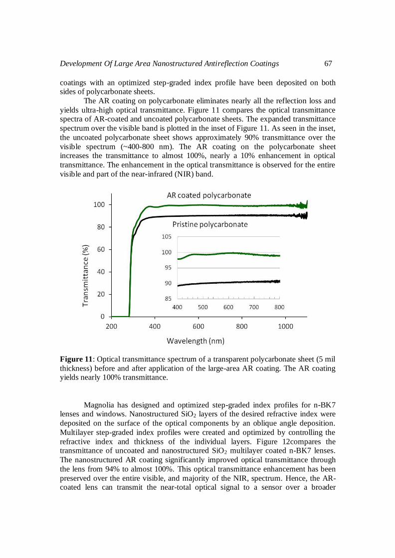
The AR coating on polycarbonate eliminates nearly all the reflection loss and
yields ultra-high optical transmittance. Figure 11 compares the optical transmittance spectra of AR-coated and uncoated polycarbonate sheets. The expanded transmittance
spectrum over the visible band is plotted in the inset of Figure 11. As seen in the inset,
the uncoated polycarbonate sheet shows approximately 90% transmittance over the
visible spectrum (~400-800 nm). The AR coating on the polycarbonate sheet increases the transmittance to almost 100%, nearly a 10% enhancement in optical
transmittance. The enhancement in the optical transmittance is observed for the entire
visible and part of the near-infrared (NIR) band.
Figure 11: Optical transmittance spectrum of a transparent polycarbonate sheet (5 mil
thickness) before and after application of the large-area AR coating. The AR coating yields nearly 100% transmittance.
Magnolia has designed and optimized step-graded index profiles for n-BK7 lenses and windows. Nanostructured SiO2 layers of the desired refractive index were
deposited on the surface of the optical components by an oblique angle deposition.
Multilayer step-graded index profiles were created and optimized by controlling the
refractive index and thickness of the individual layers. Figure 12compares the transmittance of uncoated and nanostructured SiO2 multilayer coated n-BK7 lenses.
The nanostructured AR coating significantly improved optical transmittance through
the lens from 94% to almost 100%. This optical transmittance enhancement has been
preserved over the entire visible, and majority of the NIR, spectrum. Hence, the AR-coated lens can transmit the near-total optical signal to a sensor over a broader
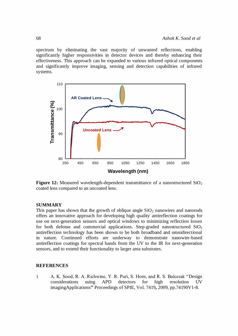
68 Ashok K. Sood et al
spectrum by eliminating the vast majority of unwanted reflections, enabling significantly higher responsivities in detector devices and thereby enhancing their
effectiveness. This approach can be expanded to various infrared optical components
and significantly improve imaging, sensing and detection capabilities of infrared systems.
Figure 12: Measured wavelength-dependent transmittance of a nanostructured SiO2
coated lens compared to an uncoated lens.
SUMMARY
This paper has shown that the growth of oblique angle SiO2 nanowires and nanorods offers an innovative approach for developing high quality antireflection coatings for
use on next-generation sensors and optical windows to minimizing reflection losses
for both defense and commercial applications. Step-graded nanostructured SiO2
antireflection technology has been shown to be both broadband and omnidirectional in nature. Continued efforts are underway to demonstrate nanowire-based
antireflection coatings for spectral bands from the UV to the IR for next-generation
sensors, and to extend their functionality to larger area substrates.
REFERENCES
1 A. K. Sood, R. A. Richwine, Y. R. Puri, S. Horn, and R. S. Balcerak “Design considerations using APD detectors for high resolution UV
imagingApplications” Proceedings of SPIE, Vol. 7419, 2009, pp.74190V1-8.
80
90
100
110
250 450 650 850 1050 1250 1450 1650 1850
Tra
ns
mit
tan
ce
(%
)
Wavelength (nm)
AR Coated Lens
Uncoated Lens

Development Of Large Area Nanostructured Antireflection Coatings 69
2 M. J. Cohen, T. J. Martin, J. C. Dries and M. J. Lange “InGaAs Sensor /Focal Plane Arrays for SWIR Applications” Proceedings of SPIE, Vol. 5406, 2004,
pp. 38-45.
3 A. K. Sood, R. A. Richwine, Y. R. Puri, N. DiLello, J. L. Hoyt, T. I. Akinwande, S. Horn, R. S. Balcerak, G. Bulman, R. Venkatasubramanian, A.
I. D'Souza, and T. G. Bramhall “Development of low dark current SiGe-
detector arrays for visible-NIR Imaging Sensor” Proceedings of SPIE, Vol.
7298, 2009, pp.72983D1-11. 4 M. Davis, J. Devitt, M. Greiner, R. Rawe, A. Timlin and D. Wade “Advanced
InSb FPA Sensor Development at CMC Electronics” Proceedings of SPIE,
Vol. 5563, 2004, pp. 62-73.
5 A. K. Sood, R. A. Richwine, Y. R. Puri, N. K. Dhar, D. L. Polla, and P. S. Wijewarnasuriya, “Multispectral EO/IR sensor model for evaluating UV,
visible, SWIR, MWIR and LWIR system performance” Proceedings of SPIE,
Vol. 7300, 2009, pp. 73000H.
6 P.W. Norton, M. Kohin, M. Dovidio and B. Becker “Commercialization of Uncooled Infrared Technology” Proceedings of SPIE, Vol. 5563, 2004, pp.
55-61.
7 A. K. Sood, R. A. Richwine, Y. R. Puri, D. L. Polla, N. K. Dhar, Z. L. Wang,
J. M. Xu, P. S. Wijewarnasuriya, N. Goldsman, M. B. Soprano, and B. Lineberry, “EO/IR sensors development using zinc oxide and carbon
nanostructures” Proceedings of SPIE, Vol. 7318, 2009, pp. 731804.
8 A. K. Sood, Y. R. Puri, L. Becker, M. Z. Tidrow, R. S. Balcerak, G. Brill, P.
Wijewarnasuriya, N. Dhar, P. Boieriu, C. Fulk, S. Sivananthan, J. Yehoda, and S. Finke. “Development of high-performance radiation-hardened antireflection
coatings for LWIR and multicolor IR focal plane arrays,” Proceedings of
SPIE, Vol. 6206, 2006, pp. 620615.
9 A. K. Sood, A. W. Sood, R. E. Welser, G. G. Pethuraja, Y. R. Puri, X. Yan, D. J. Poxson, J. Cho, E. F. Schubert, N. K. Dhar, D. L. Polla, P. Haldar, and J. L.
Harvey, “Development of Nanostructured Antireflection Coatings for EO/IR
Sensor and Solar Cell Applications,” Mater. Sci. Appl. VO-03, no. 09, p. 633,
2012. 10 A. K. Sood, G. Pethuraja, A. W. Sood, R. E. Welser, Y. R. Puri, J. Cho, E. F.
Schubert, N. K. Dhar, P. Wijewarnasuriya, and M. B. Soprano, “Development
of large area nanostructure antireflection coatings for EO/IR sensor
applications,” in Proc. SPIE 8512, Infrared Sensors, Devices, and Applications II , 2012, vol. 8512, p. 85120R–85120R–9.
11 D. J. Poxson, M.-L. Kuo, F. W. Mont, Y.-S. Kim, X. Yan, R. E. Welser, A. K.
Sood, J. Cho, S.-Y. Lin, and E. F. Schubert, “High-performance antireflection
coatings utilizing nanoporous layers,” MRS Bulletin, Vol. 36, pp. 434-438, June 2011.
12 J. Q. Xi, M.F. Schubert, J.K. Kim, E.F. Schubert, M. Chen, S.-Y. Lin, W. Liu,
and J.A. Smart “Optical Thin-Film materials with low refractive index for
broadband elimination of Fresnel reflection,” Nature Photonics, Vol. 1, 2007, pp. 176-179.

70 Ashok K. Sood et al
13 M. F. Schubert, F. W. Mont, S. Chhajed, D. J. Poxson, J. K. Kim, and E. Fred Schubert, “Design of multilayer antireflection coatings made from co-
sputtered and low-refractive-index materials by genetic algorithm,” Optics
Express, Vol. 16, pp. 5290-5298, April 2008. 14 S. Chhajed, David J. Poxson, X. Yan, J. H. Cho, E. F. Schubert, R.E. Welser,
A.K. Sood and J. K. Kim. “Nanostructured multi-layer tailored-refractive
index anti-reflection coating for glass with broadband and omni-directional
characteristics,” Applied Physics Express, Vol. 4, no. 052503, May 2011. 15 R. E. Welser, A. W. Sood, A. K. Sood, D. J. Poxson, S. Chhajed, J. Cho, E. F.
Schubert, D. L. Polla, and N. K. Dhar, “Ultra-High Transmittance through
Nanostructured-Coated Glass for Solar Cell Applications,” Proc. of SPIE, vol.
8035, no. 80350X, April 2011. 16 R. E. Welser, A. W. Sood, G. G. Pethuraja, A. K. Sood, X. Yan, D. J. Poxson,
J. Cho, E. Fred Schubert, and J. L. Harvey, “Broadband Nanostructured
Antireflection Coating on Glass for Photovoltaic Applications,” 38th IEEE
Photovoltaic Specialist Conference, no. 525, June 2012. 17 G. G. Pethuraja, A. Sood, R. Welser, A. K. Sood, H. Efstathiadis, P. Haldar,
and J. L. Harvey, “Large-area nanostructured self-assembled antireflection
coatings for photovoltaic devices,” Photovoltaic Specialists Conference
(PVSC), 2013 IEEE 39th. pp. 99–102, 2013.


![Core/Shell/Shell Nanomaterials of NaYF4: Yb, Er/Silica ...vibgyorpublishers.org/content/ijnn/ijnn-1-003.pdfand magnetic nanoparticles such as iron oxide [2,27] have been widely reported,](https://img.pdfslide.net/doc/110x75/5b1fbef37f8b9a112c8b5478/coreshellshell-nanomaterials-of-nayf4-yb-ersilica-magnetic-nanoparticles.jpg)


![¸ารกำกับดูแล... · 1. 2. 3. 4. 5. 6. 8. IJnn. IJnn. IJmn. l]nn. IJnn. (Conflict of Interest) llnn. nYJå1tuunYJlîl IJnn. nn IJmq. IJnn. IJnn. IJnn. l]nn. Govemance](https://img.pdfslide.net/doc/110x75/5f88be5d657f5364e83927d7/aaaaaaaaaaa-1-2-3-4-5-6-8-ijnn-ijnn-ijmn.jpg)