Embed Size (px)
Citation preview
Keyword(s): Abstract:
Development of New Polymer Systems and Quantum Dots - PolymerNanocomposites for Flexible OLED Display ApplicationsLihua Zhao, Zhang-Lin Zhou, Zengshan Guo, Jian Pei, Samuel Mao
HP LaboratoriesHPL-2011-68
Semi-interpenetrating polymer networks, Emissive polymers, Quantum Dots - conjugatedoligomer/polymers nanocomposites, OLEOs
Recently, tremendous progress has been made toward application of organic (small molecule/polymer)light-emitting diodes (OLEDs) in full color flat panel displays and other devices. However, with currenttechnologies, OLEDs are still struggling with high manufacturing costs which really limit the size ofOLEDs panels and with life time, especially differential aging of colors. To be more cost-effective forfabricating OLEDs, we believe solution-processing would be an attractive path due to its simplicity andhighly reduced equipment costs. This proceeding paper discusses our recent progress in development ofnew polymer systems that are highly solvent-resistant but maintaining their photophysical properties andhybrid quantum-dots (QDs)-polymer nanocomposites for their use in multicolor and multilayer OLEDspixels through solution-processing. Our new polymer systems are named conductive semi-interpenetratingpolymer networks (C-Semi-IPNs) served in different layers of OLEDs devices, containing an inert polymernetwork and conducting polymer(s) including hole transport and emissive materials. Since these do notrequire complicated chemical modification or introduction of reactive moieties to OLED materials, manystate-of-the-arts emissive polymers can be utilized to achieve RGB and white OLEDs. The researchfindings on hybrid QDoligomer nanocomposite as a good analogue lead to the successful design andsynthesis of QDpolymer nanocomposites which were used to build proof-of-the-concept devices showing agood promise in providing excellent color purity and stability as well as device robustness.
External Posting Date: May 21, 2011 [Fulltext] Approved for External PublicationInternal Posting Date: May 21, 2011 [Fulltext]
Copyright 2011 Hewlett-Packard Development Company, L.P.
Development of New Polymer Systems and Quantum Dots - Polymer Nanocomposites forFlexible OLED Display Applications
Lihua Zhao1*, Zhang-Lin Zhou1, Zengshan Guo2, Jian Pei2, Samuel Mao3
1Hewlett-Packard Labs, Hewlett-Packard Company, 1501 Page Mill Rd, Palo Alto, CA, 94304,U.S.A.
2 The Key Laboratory of Bioorganic Chemistry and Molecular Engineering of Ministry ofEducation, College of Chemistry and Molecular Engineering, Peking University, Beijing
100871, China3 Lawrence Berkeley National Laboratory and Department of Mechanical Engineering,
University of California, Berkeley, Mail Code 1740, Berkeley, CA, 94720, U.S.A.
ABSTRACT
Recently, tremendous progress has been made toward application of organic (smallmolecule/polymer) light-emitting diodes (OLEDs) in full color flat panel displays and otherdevices. However, with current technologies, OLEDs are still struggling with highmanufacturing costs which really limit the size of OLEDs panels and with life time, especiallydifferential aging of colors. To be more cost-effective for fabricating OLEDs, we believesolution-processing would be an attractive path due to its simplicity and highly reducedequipment costs. This proceeding paper discusses our recent progress in development of newpolymer systems that are highly solvent-resistant but maintaining their photophysical propertiesand hybrid quantum-dots (QDs)-polymer nanocomposites for their use in multicolor andmultilayer OLEDs pixels through solution-processing. Our new polymer systems are namedconductive semi-interpenetrating polymer networks (C-Semi-IPNs) served in different layers ofOLEDs devices, containing an inert polymer network and conducting polymer(s) including holetransport and emissive materials. Since these do not require complicated chemical modificationor introduction of reactive moieties to OLED materials, many state-of-the-arts emissive polymerscan be utilized to achieve RGB and white OLEDs. The research findings on hybrid QD-oligomer nanocomposite as a good analogue lead to the successful design and synthesis of QD-polymer nanocomposites which were used to build proof-of-the-concept devices showing a goodpromise in providing excellent color purity and stability as well as device robustness.
INTRODUCTION
Organic (Small molecule/polymer) light-emitting diodes (OLEDs) can be a greatcandidate to bring a new information display concept to our future life. Recently, tremendousprogress has been made toward application of OLEDs in full color flat panel displays and otherdevices. However, with current technologies, OLEDs are still struggling with highmanufacturing costs which really limit the size of OLEDs panels and with life time, especiallydifferential aging of colors. Besides the cost, there is still quite a long way to go for OLEDsdisplay being really flexible. Our goal is to create a display that is light weight, flexible, thin,extremely low cost, video capable, brilliant color as well as low power consumption. We believethat plastic and roll-to-roll (R2R) manufacturing will be key enablers toward this goal. Of
course, a lot of components are associated for fabricating a flexible OLEDs display. Twoimportant components are active matrix thin film transistor (TFT) backplane and OLEDs basedfrontplane. Hewlett-Packard Labs as the world-class high tech research center have developedSelf-Aligned Imprint Lithography (SAIL) method [1] so as to be the first to demonstrate low-cost fabrication of an amorphous silicon TFT backplane containing very high (sub-micro)resolution and aspect ratio with a fully R2R process on a roll of 50 um thick and 1km longplastic substrates. With our highly flexible R2R processed active matrix TFT backplanes, for theOLEDs based frontplane fabrication to be compatible with plastic and R2R manufacturing,solution-processing appears more attractive and more cost-effective due to its simplicity andhighly reduced equipment costs than vacuum deposition of small molecules by which theproduction cost increases super-linearly with the area to be coated, especially for most advancedOLEDs using multilayer structures [2-6].
One of the important issues related to solution-processing is multilayer capability.Therefore, it is of crucial importance that previously deposited layers are resistant against thesolvent used to deposit an additional layer. Two different approaches are currently applied tosuch device fabrication: 1. use of “orthogonal” solvents and a change in the polarity/solubility ofthe materials, 2. introduction of reactive moieties. However, these approaches have theirlimitations, such as limited solvent selection or synthetic compatibility, and complication. In thefirst part of this proceeding paper, we describe a general method for developing new polymersystems, named conductive semi-interpenetrating polymer networks (C-semi-IPNs) that containan inert, low-cost polymer network and conductive polymers serving different purposes inOLEDs stack. Such C-semi-IPNs can be easily incorporated into solution-processed multilayerOLEDs devices. Due to the nature of IPNs in which polymer networks are at least partiallyinterlaced on a molecular scale, the conductive polymer(s) included in these C-semi-IPNs can beprotected from subsequent layer depositions where a solvent would otherwise attack theunprotected underlying film. In addition, the formation of these C-semi-IPNs avoids thecomplexity of introducing reactive moieties to OLED materials. Our first developmentembedding a hole transporting material (HTM) into an inert cross-linked polymer network toprotect the HTM while processing the subsequent layer has been reported[7,8], and a briefsummary is included below. This technique has now been expanded to the synthesis of emissiveC-semi-IPNs (referred to E-semi-IPN below), serving as emitting layer in OLEDs devices. Ourresults included in this paper demonstrate that this synthetic method, with its broad choices formaking the suitable polymer networks, provides great opportunities to incorporate any state-of-the-art emissive polymeric materials to achieve RGB and white OLEDs. Moreover, thesematerials may be suitable for fabricating both bottom-emitting and top-emitting device structuresthat are more easily integrated onto flexible roll-to-roll printed backplanes.
As mentioned above, besides cost, the other challenge OLEDs are facing is differentialaging of colors. Organic emitting materials including both small molecules and polymers forOLEDs not only emit lights with a broad band but also age on a different pace with differentemissive colors. We had our interest to explore alternative materials to address this problem.Emissive colloidal quantum dots (QDs) are well-known for their good color purity, differentialstability and tunability as well as robustness by nature. Recently, hybrid nanocomposites basedon quantum dots (QDs) and conjugated polymers have attracted substantial attention due to theirapplications in flexible electronics, light-emitting displays [9], and photovoltaic [10]. In most ofthe previous QD-polymer nanocomposite materials, the QDs are merely physically mixed withthe polymer matrix rather than chemically attached (through chemical bonds or chemical
complexes) to the polymer material. Physically mixing CdSe/ZnS QDs with the blue-emittingelectroluminescent polymer, PFO, cannot produce an expected homogenous and uniform dispersion forgood energy transfer from PFO to QDs, therefore, the development of integrated polymer/QDs compositesystems by molecular engineering is essential. In the second part of this proceeding paper, we firstpresent in detail on our design, synthesis and characterizations of hybrid QD-oligomernanocomposites, where emitting oligomers are coordinately bonded to QDs surfaces, as a goodanalogue leading to a successful development of nanocomposites of CdSe/ZnS based QDs andamine-functionalized poly(9,9-dihexylfluorene) (PFH) derivatives. A series of characterizationstudies including photoluminescence (PL), photoluminescence excitation (PLE) andelectroluminescence (EL) measurements revealed that the efficient Förster energy exchange fromthe PFH derivative to the QDs results in an efficient red emission purely from the QDs. Theiruse in hybrid QD-polymer LEDs show a good promise in providing excellent color purity andstability as well as device robustness.
EXPERIMENTS
Synthesis of C-Semi-IPNsChemicals were purchased and used as received. For a proof-of-concept demonstration,
the preparation of C-semi-IPNs containing ADS132GE as HTM, referred to HTM C-semi-IPNbelow and pre-polymer formulations can be found in our previous reports [7, 8]. For E-semi-IPNs, we have formulated a mixture of N-vinylpyrrolidone (20%), ethoxylated bisphenol Adimethylacrylate (EBAD) (40%), trimethylolpropane trimethylacrylate (35%) and a thermalinitiator or UV initiator (5%). Toluene, as solvent, was added to the above mixture to form asolution with a concentration of 5%. Emissive polymers with many different emission colors(e.g. red, green, blue and white) can be dissolved or swollen within the solution. For example,poly(9.9-dioctylfluorenyl-2,7-diyl) (PFO, ADS129BE, American Dye Source) with aconcentration of 6 mg/mL in toluene. The well-mixed solution undergoes polymerization to givea cross-linked network to provide E-semi-IPNs as expected.
Synthesis of functionalized oligofluorene, polyfluorene derivatives and correspondinghybrid nanocomposites with CdSe/ZnS core-shell QDs
Starting materials were purchased and used as received. The key intermediate 6 p-2-(7-Bromo-9,9-di-n-octylfluorene)benzyl-Di-n-Octylphosphine Oxide (Br-DOF-Bn-DOPO) wassynthesized from 2,7-dibromo-9,9-di-n-octylfluorene via four key steps with an overall yield ofabout 42%. Functionalized oligofluorene (trimer: Bis-DOPO-Bn-tri-Dioctylfluorene(BDBTFO)) was then synthesized via coupling reaction between Br-DOF-Bn-DOPO (0.270 g,0.324 mmol) and 9,9’-Dioctylfluorene-2,7-Bis(trimethylene Borate) (0.082 g, 0.147 mmol) intoluene in the presence of degassed K2CO3 (0.082g, 0.59 mmol) aqueous solution (1.5 mL H2O)under Argon at room temperature using Pd(PPh3)4 (8.5 mg, 0.074 mmol) as catalyst. Afterpurification of the cruel material obtained from the recation by column chromatography (EtOAc:Hexane = 2:1 to 2% MeOH in EtOAc), the product BDBTFO was given as a white solid (0.140g, 50%). This BDBFTO was then added to a solution of pyridine-capped CdSe/ZnS QD (5mg/mL) in THF. After stirring overnight at 65 ºC in the glovebox, MeOH was added toprecipitate out QD-BDBTFO nanocomposite. The collected precipitate was washed with MeOHand then dissolved into 1 mL of CHCl3. The resulting QD-BDBTDO solution was used forfurther study. Detailed synthetic experiments and materials characterization of oligofluorene
(BDBTFO) and QD-BDBTFO hybrid nanocomposite will be reported elsewhere. Amine-functionalized polyfluorene derivatives and corresponding QD-polymer nanocomposites weresynthesized, fully characterized by 1H and 13C NMR, UV-vis and photoluminescentspectroscopy, gel permeation chromatography, elemental analyses and reported in our publishedpaper [11].
Physical CharacterizationAbsorption spectra were recorded on Cary 6000i UV-vis-NIR spectrometer. PL and EL
spectrum was recorded on JobinYvon Triax 550 Spectrometer. PLE measurements were alsotaken on Cary 6000i UV-vis-NIR spectrometer with some customized modification.Transmission electron microscopy (TEM) was performed on a Philips CM300FEG operating at300 keV using zero loss energy filtering with Gatan CCD for images. Scanning electronmicroscopy (SEM) was carried out using a Hitachi S-4500 cold field emission microscope.
Device FabricationFor a proof-of-the-concept demonstration, we have chosen a very simple OLEDs device
configuration of ITO-PET or glass/PEDOT-PSS or DuPont Buffer (DB)/(C-semi-IPNs as holetransport layer, optional)/polymer, E-Semi-IPNs or hybrid nanocomposite/Al. The ITO-coatedglass or PET substrates was cleaned with O2 and CF4 plasma. PEDOT:PSS or DB was coated byspin casting and dried at 100 °C for an hour to give a smooth film of 45 nm. The films (60-80nm) of polymers, C-semi-IPNs, or hybrid nanocomposites were coated by spin casting fromsolutions on top of PEDOT or DB, respectively. Then Al film (~120 nm) as cathode wasthermally evaporated in a vacuum chamber under a pressure of 4 ×10⁻⁵ Torr through shadowmasks to give a finished OLEDs stack.
DISCUSSION
Semi-Interpenetrating Polymer Networks
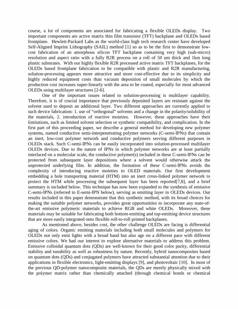
A general methodology for the synthesis of C-semi-IPNs is developed and shown inFigure 1 via a sequential method. X is a mixture of the cross-linkable monomers, oligomers orpolymers containing cross-linking agent(s) and initiator or initiators. Cross-linking agents can be2-branch, 3-branch, or 4-branch cross-linkers that are initiated with energy appropriate to eitherthermal or photo initiators. Conductive polymer(s) including hole transport materials andemissive materials with many different emission colors (e.g. red, green, blue and white) (referredto herein as “A” based polymers) can be dissolved or swollen within the X-solution.
A
A
A
AA
A
Semi-IPN
A
A
A
A
A
AX
XXX
XX
X
X
XX
A
A
A
X
X
X
X
X
A
A
A
AA
A
A
A
A
A
A
A X
XXX
XX
X
X
XX
A
A
A
X
X
X
X
X
Cross-linkingpolymerization
Figure 1. Formation of C-semi-IPN via sequential method
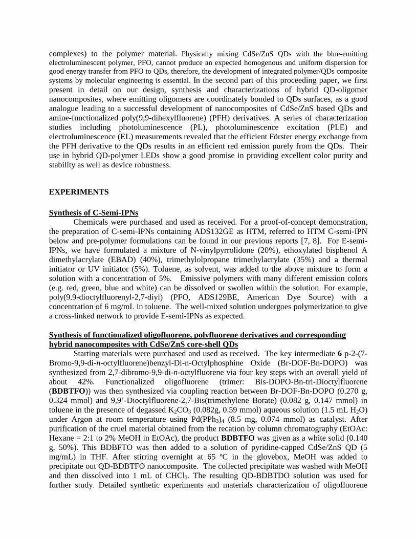
In our previous report [7, 8], ADS132GE as hole transport materials (HTM)interpenetrated into a cross-linked polymer network shown in Figure 1a. This cross-linked
polymer network mostly preserved the desired optical and electrical properties of the HTM andmaintains the morphology of the embedded polymer film after the solvent (which is used foradditional layer deposition) washing. This is verified by corresponding PL measurement andAFM images shown in Figure 1b and 1c.
a.
N
n-C4H9
n
HTL: ADS132GE
Mix with commercially available curing agent
HTL uniformly distributed within cross-linked polymer matrix b. c.Figure 2. a. Scheme of synthesis HTM C-semi-IPNs; b. PL spectra of HTM C-semi-IPNs beforeand after solvent washing; c. AFM images of HTM C-semi-IPNs.
A number of OLED devices were fabricated and tested using HTM C-semi-IPNs as holetransport layer (HTL) with subsequent layer of ADS129BE as emissive layer (EML) in OLEDstack. Advantages offered by this HTL were clearly seen that the electroluminescence efficiencyis improved greatly, with a significant reduction of leakage current, by more balanced electronand hole injection in the devices, which demonstrate the effectiveness of HTM C-semi-IPNs [8].
With the inspiration of these research findings, this technique has now been expanded tothe preparation of emissive-semi-IPNs (referred as E-semi-IPN below) in which conductivepolymers are emitting conjugated polymers. The resulting materials are used to serve as emittinglayers in OLEDs devices. For a proof-of-concept demonstration, the formulated solution withADS129BE as emissive material example undergoes thermally-initiated polymerization to give across-linked network to provide E-semi-IPNs as expected. This set of materials does notnecessarily represent the best formulation, but it suffices for demonstrating the advantages of E-semi-IPNs for OLED applications. PFO-only thin films and devices are used as control forevaluating blue-emitting E-semi-IPNs.
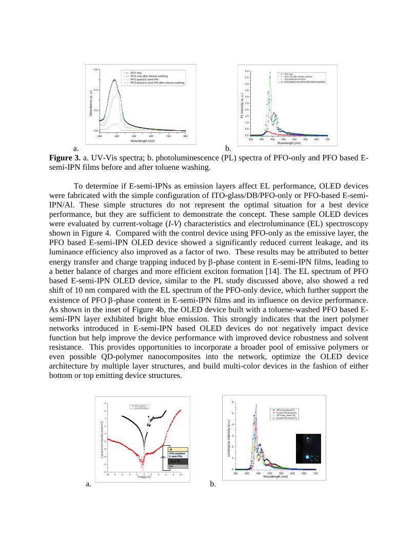
The solvent resistances of thin films of PFO-only and PFO-based E-semi-IPN on DBcoated ITO glass were characterized through UV-Vis absorption and photoluminescence (PL)spectroscopy, as shown in Figure 3. After toluene washing, the UV-Vis absorbance of E-semi-IPN film remains over 85% of its original film value while the UV-Vis absorbance of PFO-onlyfilm decrease by over 95% (Figure 3a). Even more importantly, the PL intensity of E-semi-IPNfilm remains the same as before toluene washing, compared with almost none emission from thetoluene-washed PFO-only film. The over 10% loss of UV-vis absorption from PFO based E-semi-IPN film after toluene washing may attribute to the removal of PFO that was staying on thesurface of interpenetrating polymer networks but not interlaced with those highly crosslinkedpolymer networks. Moreover, E-semi-IPN film shows a higher PL intensity than PFO-only filmseven though the PFO absorbance (both peak and integral) of E-semi-IPN films is lower than PFOonly films (Figure 3b). This indicates that E-semi-IPNs have better internal emission efficiency,which is one of their important advantages over polymer-only emitters when used in OLEDs.Compared with PFO-only films, PFO based E-semi-IPN films appear to have red-shiftedabsorption and emission which result from the formation of a PFO -phase component.Increased -phase content has also been linked to an increase in the ratio of singlet to tripletexcitons, a decrease in photobleaching, and improved hole mobility [12, 13].
a.
300 400 500 600 700 800
0.0
0.2
0.4
0.6
Absorb
ance
(a.u.)
Wavelength (nm)
PFO onlyPFO only-after toluene washingPFO based E-semi-IPNPFO based E-semi-IPN-after toluene washing
b.
350 400 450 500 550 600 650 700
0.0
0.5
1.0
1.5
2.0
2.5
3.0
3.5
4.0
4.5
5.0
PL
Inte
nsity
(a.u
.)
Wavelength (nm)
PFO onlyPFO only after toluene washingPFO based E-semi-IPNPFO based E-semi-IPN after toluene washing
Figure 3. a. UV-Vis spectra; b. photoluminescence (PL) spectra of PFO-only and PFO based E-semi-IPN films before and after toluene washing.
To determine if E-semi-IPNs as emission layers affect EL performance, OLED deviceswere fabricated with the simple configuration of ITO-glass/DB/PFO-only or PFO-based E-semi-IPN/Al. These simple structures do not represent the optimal situation for a best deviceperformance, but they are sufficient to demonstrate the concept. These sample OLED deviceswere evaluated by current-voltage (I-V) characteristics and electroluminance (EL) spectroscopyshown in Figure 4. Compared with the control device using PFO-only as the emissive layer, thePFO based E-semi-IPN OLED device showed a significantly reduced current leakage, and itsluminance efficiency also improved as a factor of two. These results may be attributed to betterenergy transfer and charge trapping induced by -phase content in E-semi-IPN films, leading toa better balance of charges and more efficient exciton formation [14]. The EL spectrum of PFObased E-semi-IPN OLED device, similar to the PL study discussed above, also showed a redshift of 10 nm compared with the EL spectrum of the PFO-only device, which further support theexistence of PFO -phase content in E-semi-IPN films and its influence on device performance.As shown in the inset of Figure 4b, the OLED device built with a toluene-washed PFO based E-semi-IPN layer exhibited bright blue emission. This strongly indicates that the inert polymernetworks introduced in E-semi-IPN based OLED devices do not negatively impact devicefunction but help improve the device performance with improved device robustness and solventresistance. This provides opportunities to incorporate a broader pool of emissive polymers oreven possible QD-polymer nanocomposites into the network, optimize the OLED devicearchitecture by multiple layer structures, and build multi-color devices in the fashion of eitherbottom or top emitting device structures.
a.
-10 -8 -6 -4 -2 0 2 4 6 8 10
-6
-5
-4
-3
-2
-1
0
1
2
3
Lo
g(C
urr
entIn
tensity
(mA
/cm
2))
Voltage (V)
PFO only device
E-semi-IPNs device
Al
ITO
DB as HIL
PFO containedE-semi-IPNs
AlAl
ITO
DB as HIL
PFO containedE-semi-IPNs
b.
350 400 450 500 550 600 650 700
0
1
2
3
4
5
6
Lu
min
an
ceIn
ten
sity
(a.u
.)
Wavelength (nm)
PFO only device ELE-semi-IPN device ELPFO only device PLE-semi-IPN device PL
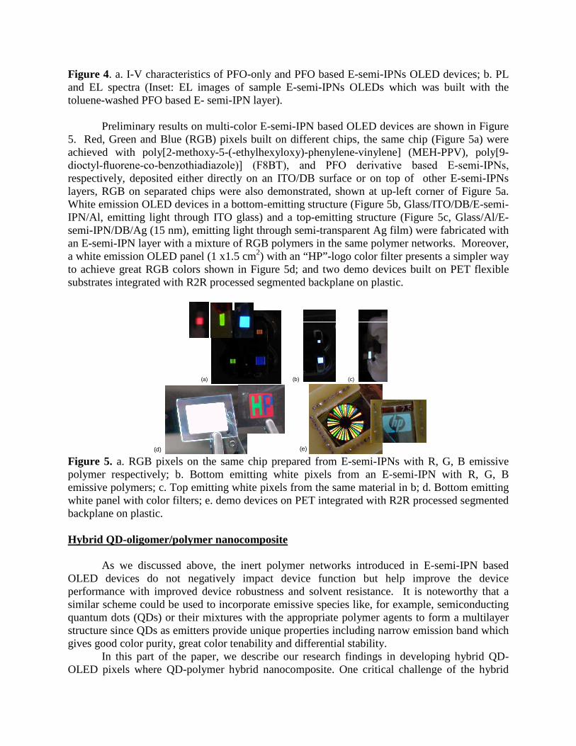
Figure 4. a. I-V characteristics of PFO-only and PFO based E-semi-IPNs OLED devices; b. PLand EL spectra (Inset: EL images of sample E-semi-IPNs OLEDs which was built with thetoluene-washed PFO based E- semi-IPN layer).
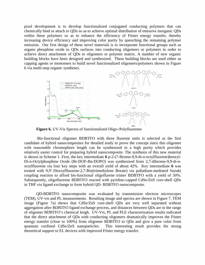
Preliminary results on multi-color E-semi-IPN based OLED devices are shown in Figure5. Red, Green and Blue (RGB) pixels built on different chips, the same chip (Figure 5a) wereachieved with poly[2-methoxy-5-(-ethylhexyloxy)-phenylene-vinylene] (MEH-PPV), poly[9-dioctyl-fluorene-co-benzothiadiazole)] (F8BT), and PFO derivative based E-semi-IPNs, respectively, deposited either directly on an ITO/DB surface or on top of other E-semi-IPNslayers, RGB on separated chips were also demonstrated, shown at up-left corner of Figure 5a.White emission OLED devices in a bottom-emitting structure (Figure 5b, Glass/ITO/DB/E-semi-IPN/Al, emitting light through ITO glass) and a top-emitting structure (Figure 5c, Glass/Al/E-semi-IPN/DB/Ag (15 nm), emitting light through semi-transparent Ag film) were fabricated withan E-semi-IPN layer with a mixture of RGB polymers in the same polymer networks. Moreover,a white emission OLED panel (1 x1.5 cm2) with an “HP”-logo color filter presents a simpler wayto achieve great RGB colors shown in Figure 5d; and two demo devices built on PET flexiblesubstrates integrated with R2R processed segmented backplane on plastic.
(a) (b) (c)
(d) (e)
Figure 5. a. RGB pixels on the same chip prepared from E-semi-IPNs with R, G, B emissivepolymer respectively; b. Bottom emitting white pixels from an E-semi-IPN with R, G, Bemissive polymers; c. Top emitting white pixels from the same material in b; d. Bottom emittingwhite panel with color filters; e. demo devices on PET integrated with R2R processed segmentedbackplane on plastic.
Hybrid QD-oligomer/polymer nanocomposite
As we discussed above, the inert polymer networks introduced in E-semi-IPN basedOLED devices do not negatively impact device function but help improve the deviceperformance with improved device robustness and solvent resistance. It is noteworthy that asimilar scheme could be used to incorporate emissive species like, for example, semiconductingquantum dots (QDs) or their mixtures with the appropriate polymer agents to form a multilayerstructure since QDs as emitters provide unique properties including narrow emission band whichgives good color purity, great color tenability and differential stability.
In this part of the paper, we describe our research findings in developing hybrid QD-OLED pixels where QD-polymer hybrid nanocomposite. One critical challenge of the hybrid
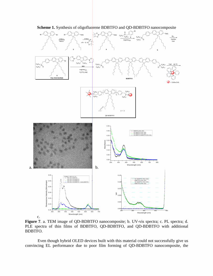
pixel development is to develop functionalized conjugated conducting polymers that canchemically bind or attach to QDs so as to achieve optimal distribution of emissive inorganic QDswithin these polymers so as to enhance the efficiency of Föster energy transfer, therebyincreasing device efficiency and improving color purity by quenching the remaining polymeremission. Our first design of these novel materials is to incorporate functional groups such asorgano phosphine oxide to QDs surfaces into conducting oligomers or polymers in order toachieve direct attachment of QDs to oligomers or polymer matrix. A number of new organicbuilding blocks have been designed and synthesized. These building blocks are used either ascapping agents or monomers to build novel functionalized oligomers/polymers shown in Figure6 via multi-step organic syntheses.
250 300 350 400 450 5000.0
0.5
1.0
1.5
2.0
2.5
332 nm
Ab
sorb
an
ce
Wavelength (nm)
BDBTOF (3 units)BDBD(1 unit)MPFH (50-100 units)
391 nm
364 nm
d e m o d e m o d e m o d e m o d e m o
d e m o d e m o d e m o d e m o d e m o
d e m o d e m o d e m o d e m o d e m o
d e m o d e m o d e m o d e m o d e m o
d e m o d e m o d e m o d e m o d e m o
d e m o d e m o d e m o d e m o d e m o
d e m o d e m o d e m o d e m o d e m o
BDBTFO
P
O
C8H17
C8H17
P
OC8H17
C8H17
BDBD
P
O
C8H17
C8H17n
Br
MPFH
PPO OC8H17
C8H17 C8H17
C8H17
Figure 6. UV-Vis Spectra of functionalized Oligo-/Polyfluorenes
Bis-functional oligomer BDBTFO with three fluorene units is selected as the firstcandidate of hybrid nanocomposites for detailed study to prove the concept since this oligomerwith reasonable chromophore length can be synthesized in a high purity which providesrelatively easier control for preparing hybrid nanocomposite. The synthesis of this new materialis shown in Scheme 1. First, the key intermediate 6 p-2-(7-Bromo-9,9-di-n-octylfluorene)benzyl-Di-n-Octylphosphine Oxide (Br-DOF-Bn-DOPO) was synthesized from 2,7-dibromo-9,9-di-n-octylfluorene via four key steps with an overall yield of about 42%. Key intermediate 6 wastreated with 9,9’-Dioctylfluorene-2,7-Bis(trimethylene Borate) via palladium-mediated Suzukicoupling reaction to afford bis-functional oligoflurene trimer BDBTFO with a yield of 50%.Subsequently, oligofluorene BDBTFO reacted with pyridine-capped CdSe/ZnS core-shell QDsin THF via ligand exchange to form hybrid QD- BDBTFO nanocomposite.
QD-BDBTFO nanocomposite was evaluated by transmission electron microscopes(TEM), UV-vis and PL measurements. Resulting image and spectra are shown in Figure 7. TEMimage (Figure 7a) shows that CdSe/ZnS core-shell QDs are very well separated withoutaggregation after BDBTFO ligand exchange process, and distances between QDs are in the rangeof oligomer BDBTFO’s chemical lengh. UV-Vis, PL and PLE characterization results indicatedthat the direct attachment of QDs with conducting oligomers dramatically improves the Fösterenergy transfer (close to 100%) from oligomer BDBTFO to QDs and give a pure color fromquantum confined CdSe/ZnS nanoparticles. This interesting result provides the strongtheoretical support to EL devices with improved Föster energy transfer.
Scheme 1. Synthesis of oligofluorene BDBTFO and QD-BDBTFO nanocomposite
BrBr
n-BuLi
TMSCl
TMSBr
n-BuLi
B
O
OOi-Pr
TMSBO
O
P
O
C8H17C8H17
Br
Pd(PPh3)4
TMS
PO
C8H17
C8H17
Br2
NaOAc
Br
PO
C8H17
C8H17
Key Intermediate
THF
3 4
2
5
6
BB
C8H17 C8H17
O
OO
O
$$$
K2CO3 (aq)
Pd(PPh3)4
PO
C8H17
C8H17
PO
C8H17
C8H17
BDBTFO
N
PO
C8H17
C8H17
P O
C8H17
C8H17
THF 65 oC
n = 3
n
NN
NN
CdSe-ZnS=
QD-BDBTFO
a. b.
200 300 400 500 600 700 800
0.00
0.05
0.10
0.15
0.20
0.25
0.30
0.35
Absorb
ance
Wavelength (nm)
BDBTFO (Film 323)NC-BDBTFO (Film 324)NC-BDBTFO (Film 325)NC-BDBTFO+BDBTFO (Film 321)
c.
350 400 450 500 550 600 650 700
0.15
0.20
0.25
0.30
0.35
0.40
0.45
Flu
ore
scen
ceIn
tensity
(Mic
roA
mps)
Wavelength (nm)
Grating: 3, Slit: 0.5, 0.5Film 323, BDBTFOFilm 324, NC-BDBTFOFilm 325, NC-BDBTFOFilm 321, NC-BDBTFO + Extra BDBTFO
200 300 400 500 600
0.000
0.025
0.050
0.075
0.100
0.125
%R
Wavelength (nm)
NC-BDBTFO (Film 324)BDBTFO (Film 323)NC-BDBTFO (Film 325)BDBTFO (Film 323)
d e m o d e m o d e m o d e m o d e m o
d e m o d e m o d e m o d e m o d e m o
d e m o d e m o d e m o d e m o d e m o
d e m o d e m o d e m o d e m o d e m o
d e m o d e m o d e m o d e m o d e m o
d e m o d e m o d e m o d e m o d e m o
d e m o d e m o d e m o d e m o d e m o
Figure 7. a. TEM image of QD-BDBTFO nanocomposite; b. UV-vis spectra; c. PL spectra; d.PLE spectra of thin films of BDBTFO, QD-BDBTFO, and QD-BDBTFO with additionalBDBTFO.
Even though hybrid OLED devices built with this material could not successfully give usconvincing EL performance due to poor film forming of QD-BDBTFO nanocomposite, the
research findings of QD-BDBTFO nanocomposite are still encouraging, which leads us to afurther development on this subject. We have reported a few series of functionalizedpolyfluorene derivatives, which might have great utility to prepare QD-polymer nanocompositeshown in Scheme 2 [11, 15, 16]. Amine-functionlized poly(9,9-dihexylfluorene) (PFH)derivatives are presented here as an example. Five amine-functionaized conjugated PFHcopolymers were synthesized with different composition, which were fully characterized andshowed great thermal stability up to 220 ºC. The detailed study of their photophysical andelectrochemical properties has been reported [11]. From the electrochemical data, it wasestimated that band gap of these functionalized polymers was around 2.70 to 3.07 ev for P1-P5,which made them good candidates as host materials for QD-polymer hybrid nanocomposites.
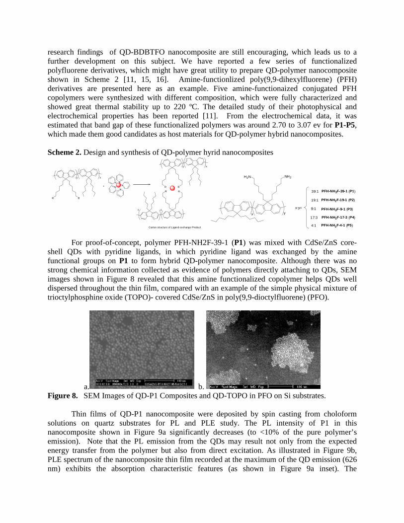
Scheme 2. Design and synthesis of QD-polymer hyrid nanocomposites
R R
y x
NN
N
N
N
+
y x
RR
R R
yx
Carton structure of Ligand-exchange Product
NH2H2N
x y
x:y=
39:1 PFH-NH2F-39-1 (P1)
19:1 PFH-NH2F-19-1 (P2)
9:1 PFH-NH2F-9-1 (P3)
17:3 PFH-NH2F-17-3 (P4)
4:1 PFH-NH2F-4-1 (P5)
For proof-of-concept, polymer PFH-NH2F-39-1 (P1) was mixed with CdSe/ZnS core-shell QDs with pyridine ligands, in which pyridine ligand was exchanged by the aminefunctional groups on P1 to form hybrid QD-polymer nanocomposite. Although there was nostrong chemical information collected as evidence of polymers directly attaching to QDs, SEMimages shown in Figure 8 revealed that this amine functionalized copolymer helps QDs welldispersed throughout the thin film, compared with an example of the simple physical mixture oftrioctylphosphine oxide (TOPO)- covered CdSe/ZnS in poly(9,9-dioctylfluorene) (PFO).
a. b.Figure 8. SEM Images of QD-P1 Composites and QD-TOPO in PFO on Si substrates.
Thin films of QD-P1 nanocomposite were deposited by spin casting from choloformsolutions on quartz substrates for PL and PLE study. The PL intensity of P1 in thisnanocomposite shown in Figure 9a significantly decreases (to <10% of the pure polymer’semission). Note that the PL emission from the QDs may result not only from the expectedenergy transfer from the polymer but also from direct excitation. As illustrated in Figure 9b,PLE spectrum of the nanocomposite thin film recorded at the maximum of the QD emission (626nm) exhibits the absorption characteristic features (as shown in Figure 9a inset). The
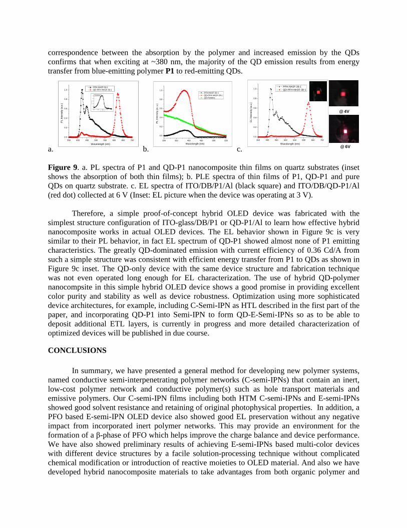
correspondence between the absorption by the polymer and increased emission by the QDsconfirms that when exciting at ~380 nm, the majority of the QD emission results from energytransfer from blue-emitting polymer P1 to red-emitting QDs.
a.
350 400 450 500 550 600 650 700
0.0
0.2
0.4
0.6
0.8
1.0
PL
Inte
nsi
ty(a
.u.)
Wavelength (nm)
PFH-NH2F-39-1QD-PFH-NH2F-39-1
300 350 400 450 5000.0
0.2
0.4
0.6
0.8
1.0
Abs
or
ba
nce
W ave l ength (nm)
PFH-N H2F-39-1QD -PFH-NH2F-39-1
b.
300 350 400 450 500 550
0.0
0.2
0.4
0.6
0.8
1.0
PL
Inte
nsi
ty(a
.u.)
Wavelength (nm)
PFH-NH2F-39-1QD-PFH-NH2F-39-1QD-Pyridine
c.
350 400 450 500 550 600 650 700
0.0
0.2
0.4
0.6
0.8
1.0
EL
Inte
nsity
(a.u
.)
Wavelength (nm)
PFH-NH2F-39-1QD-PFH-NH2F-39-1
@ 4V
@ 6V
Figure 9. a. PL spectra of P1 and QD-P1 nanocomposite thin films on quartz substrates (insetshows the absorption of both thin films); b. PLE spectra of thin films of P1, QD-P1 and pureQDs on quartz substrate. c. EL spectra of ITO/DB/P1/Al (black square) and ITO/DB/QD-P1/Al(red dot) collected at 6 V (Inset: EL picture when the device was operating at 3 V).
Therefore, a simple proof-of-concept hybrid OLED device was fabricated with thesimplest structure configuration of ITO-glass/DB/P1 or QD-P1/Al to learn how effective hybridnanocomposite works in actual OLED devices. The EL behavior shown in Figure 9c is verysimilar to their PL behavior, in fact EL spectrum of QD-P1 showed almost none of P1 emittingcharacteristics. The greatly QD-dominated emission with current efficiency of 0.36 Cd/A fromsuch a simple structure was consistent with efficient energy transfer from P1 to QDs as shown inFigure 9c inset. The QD-only device with the same device structure and fabrication techniquewas not even operated long enough for EL characterization. The use of hybrid QD-polymernanocompsite in this simple hybrid OLED device shows a good promise in providing excellentcolor purity and stability as well as device robustness. Optimization using more sophisticateddevice architectures, for example, including C-Semi-IPN as HTL described in the first part of thepaper, and incorporating QD-P1 into Semi-IPN to form QD-E-Semi-IPNs so as to be able todeposit additional ETL layers, is currently in progress and more detailed characterization ofoptimized devices will be published in due course.
CONCLUSIONS
In summary, we have presented a general method for developing new polymer systems,named conductive semi-interpenetrating polymer networks (C-semi-IPNs) that contain an inert,low-cost polymer network and conductive polymer(s) such as hole transport materials andemissive polymers. Our C-semi-IPN films including both HTM C-semi-IPNs and E-semi-IPNsshowed good solvent resistance and retaining of original photophysical properties. In addition, aPFO based E-semi-IPN OLED device also showed good EL preservation without any negativeimpact from incorporated inert polymer networks. This may provide an environment for theformation of a β-phase of PFO which helps improve the charge balance and device performance.We have also showed preliminary results of achieving E-semi-IPNs based multi-color deviceswith different device structures by a facile solution-processing technique without complicatedchemical modification or introduction of reactive moieties to OLED material. And also we havedeveloped hybrid nanocomposite materials to take advantages from both organic polymer and
quantum dots region. Our research findings from QD-oligomer BDBTFO supported chemicallybonding together between QDs and this functional oligomer provides good energy transfer (closeto 100%) from oligomer BDBTFO to QDs and give a pure color from quantum confinedCdSe/ZnS nanoparticles. Such a chemical system served as a good analogue directly leaded to adevelopment of functionalized conducting polymers and their corresponding hybrid QD-polymercomposites. Our selected QD-P1 hybrid material showed a good promise in providing excellentcolor purity and stability as well as device robustness. More detailed work on further understandbasics, optimizing materials formulation and device structures and improving deviceperformance are currently underway.
ACKNOWLEDGMENTS
This work was supported by Hewlett-Packard Company and National NSF of China.Thanks to colleagues of Information Surface Lab at HP Labs for great support and valuablediscussion.
REFERENCES
1. Thin Film Devices and Methods for Forming the Same. US Patent 7541227.2. Klaus M_llen, Ullrich Scherf, Organic Light Emitting Devices: Synthesis, Properties and
Applications, Wiley-VCH, Verlag GmbH & Co. KGaA, Weinheim, 2006, pg. 151.3. T. R. Herbner, C. C. Wu, D. Marcy, M. H. Lu, J. C. Strum, Applied Physics Letter, 72,
519 (1998).4. G. Gustafsson, Y. Gao, G. M. Treacy, F. Klavetter, N. Colaneri, A. J. Heeger, Nature,
357, 477, (1992).5. S. R. Forrest, Nature, 428, 911, (2004).6. R. Kiebooms, R. Menon, and K. Lee, Handbook of Advanced Electronic and Photonic
Materials and Devices, edited by H. S. Nalwa _Academic, San Diego, 2001,Vol. 8, pg. 1.7. Z. L. Zhou, X. Sheng, K. Nauka, L. Zhao, G. Gibson, S. Lam, C. Yang, J. Brug, and R.
Elder, Applied Physics Letter, 96, 013504, (2010) and references therein.8. Z. L. Zhou, X. Sheng, L. Zhao, G. Gibson, S. Lam, K. Nauka, J. Brug MRS Symposium
B Proceedings Paper, 1154, 1154-B10-108, (2009) and references therein.9. (a) V. L. Colvin, M. C. Schlamp, A. P. Alivisatos, Nature, 370, 354, (1994). (b) B. O.
Dabbousi, M. G. Bawendi, O. Onitsuka, M. F. Rubner, Appl. Phys. Lett., 66, 1316,(1995). (c) T.-W. F. Chang, S. Musikhin, L. Bakueva, L. Levina,; M. A. Hines, P. W.Cyr,; E. H. Sargent, Appl. Phys. Lett. 84, 4295, (2004).
10. (a) W. U. Huynh, J. J. Dittmer, A. P. Alivisatos, Science, 295, 2425 (2002). (b) S. A.McDonald, G. Konstantatos, S. G. Zhang, P. W. Cyr, E. J. D. Klem, L. Levina, E. H.Sargent, Nat. Mater., 4, 138, (2005). (c) J. Liu, T. Tanaka, K. Sivula, A. P. Alivisatos, J.M. Frechet, J. Am. Chem. Soc., 126, 6550 (2004).
11. Z. Guo, L. Zhao, J. Pei, Z. L. Zhou, G. Gibson, S. Lam, J. Brug, S. S. MaoMacromolecules, 43(4), 1860-1866 (2010) and references therein.
12. J. Peet, E. Brocker, Y. Xu, G. C. Bazan, Advanced Materials, 20, 1882, (2008).13. M. Ariu, M. Sima, M. D. Rahn, J. Hill, A. M. Fox, D. G. Lidzey, M. Oda, J. Cabanillas-
Gonzalez, D. D. C. Bradley, Physics Review. B, 67, 195333 (2003).14. H. H. Lu, C. Y. Liu, C. H. Chang, S. A. Chen, Advanced Materials, 19, 2574 (2007).15. Z. Guo, J. Pei, Z. L. Zhou, L. Zhao, G. Gibson, S. Lam, and J. Brug Polymer, 50(20),
4794-4800(2009).16. Z. Guo, D. Liu, C. Wang, J. Pei, Z. L. Zhou, L. Zhao, G. Gibson, J. Brug, S. Lam, S. Mao
Science China Chemistry, 54(4), 678-684 (2011).