Embed Size (px)
Citation preview
FN3284Rev 11.00
Nov 20, 2006
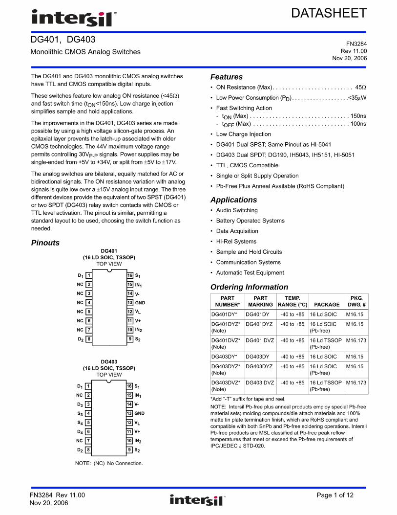
DG401, DG403Monolithic CMOS Analog Switches
DATASHEET
The DG401 and DG403 monolithic CMOS analog switches have TTL and CMOS compatible digital inputs.
These switches feature low analog ON resistance (<45) and fast switch time (tON<150ns). Low charge injection simplifies sample and hold applications.
The improvements in the DG401, DG403 series are made possible by using a high voltage silicon-gate process. An epitaxial layer prevents the latch-up associated with older CMOS technologies. The 44V maximum voltage range permits controlling 30VP-P signals. Power supplies may be single-ended from +5V to +34V, or split from 5V to 17V.
The analog switches are bilateral, equally matched for AC or bidirectional signals. The ON resistance variation with analog signals is quite low over a 15V analog input range. The three different devices provide the equivalent of two SPST (DG401) or two SPDT (DG403) relay switch contacts with CMOS or TTL level activation. The pinout is similar, permitting a standard layout to be used, choosing the switch function as needed.
PinoutsDG401
(16 LD SOIC, TSSOP)TOP VIEW
DG403 (16 LD SOIC, TSSOP)
TOP VIEW
NOTE: (NC) No Connection.
Features• ON Resistance (Max). . . . . . . . . . . . . . . . . . . . . . . . . 45
• Low Power Consumption (PD) . . . . . . . . . . . . . . . . . . .<35W
• Fast Switching Action- tON (Max) . . . . . . . . . . . . . . . . . . . . . . . . . . . . . . . 150ns- tOFF (Max) . . . . . . . . . . . . . . . . . . . . . . . . . . . . . . 100ns
• Low Charge Injection
• DG401 Dual SPST; Same Pinout as HI-5041
• DG403 Dual SPDT; DG190, IH5043, IH5151, HI-5051
• TTL, CMOS Compatible
• Single or Split Supply Operation
• Pb-Free Plus Anneal Available (RoHS Compliant)
Applications• Audio Switching
• Battery Operated Systems
• Data Acquisition
• Hi-Rel Systems
• Sample and Hold Circuits
• Communication Systems
• Automatic Test Equipment
14
15
16
9
13
12
11
10
1
2
3
4
5
7
6
8
D1
NC
NC
NC
NC
NC
D2
NC
S1
V-
GND
VL
V+
IN2
S2
IN1
14
15
16
9
13
12
11
10
1
2
3
4
5
7
6
8
D1
NC
D3
S3
S4
D4
D2
NC
S1
V-
GND
VL
V+
IN2
S2
IN1
Ordering InformationPART
NUMBER*PART
MARKINGTEMP.
RANGE (°C) PACKAGEPKG.
DWG. #
DG401DY* DG401DY -40 to +85 16 Ld SOIC M16.15
DG401DYZ*(Note)
DG401DYZ -40 to +85 16 Ld SOIC(Pb-free)
M16.15
DG401DVZ*(Note)
DG401 DVZ -40 to +85 16 Ld TSSOP (Pb-free)
M16.173
DG403DY* DG403DY -40 to +85 16 Ld SOIC M16.15
DG403DYZ*(Note)
DG403DYZ -40 to +85 16 Ld SOIC(Pb-free)
M16.15
DG403DVZ*(Note)
DG403 DVZ -40 to +85 16 Ld TSSOP (Pb-free)
M16.173
*Add “-T” suffix for tape and reel.
NOTE: Intersil Pb-free plus anneal products employ special Pb-free material sets; molding compounds/die attach materials and 100% matte tin plate termination finish, which are RoHS compliant and compatible with both SnPb and Pb-free soldering operations. Intersil Pb-free products are MSL classified at Pb-free peak reflow temperatures that meet or exceed the Pb-free requirements of IPC/JEDEC J STD-020.
FN3284 Rev 11.00 Page 1 of 12Nov 20, 2006
DG401, DG403
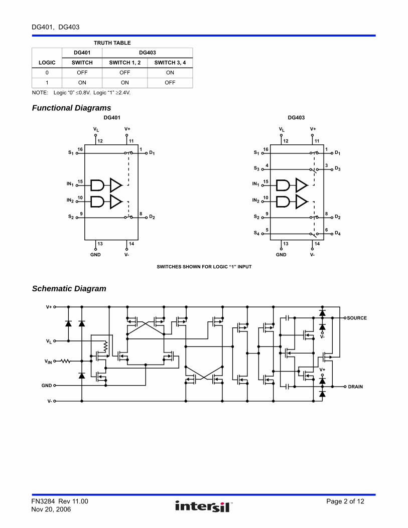
Schematic Diagram
TRUTH TABLE
LOGIC
DG401 DG403
SWITCH SWITCH 1, 2 SWITCH 3, 4
0 OFF OFF ON
1 ON ON OFF
NOTE: Logic “0” 0.8V. Logic “1” 2.4V.
Functional DiagramsDG401 DG403
SWITCHES SHOWN FOR LOGIC “1” INPUT
15
10
9
16
8
1S1
IN1
IN2
S2
D1
D2
VL V+
GND V-
12 11
13 14
15
10
9
4
16
5
8
3
1
6
S1
S3
IN1
IN2
S2
S4
D1
D3
D2
D4
VL V+
GND V-
12 11
13 14
V-
V+
V+
VL
VIN
GND
V-
DRAIN
SOURCE
FN3284 Rev 11.00 Page 2 of 12Nov 20, 2006
DG401, DG403
Absolute Maximum Ratings Thermal Information
V+ to V- . . . . . . . . . . . . . . . . . . . . . . . . . . . . . . . . . . . . . . . . . . 44.0VGND to V-. . . . . . . . . . . . . . . . . . . . . . . . . . . . . . . . . . . . . . . . . . 25VVL. . . . . . . . . . . . . . . . . . . . . . . . . . . . . . (GND - 0.3V) to (V+) +0.3VDigital Inputs VS, VD (Note 1) . . . . . (V-) -2V to (V+) + 2V or 30mA,
Whichever Occurs FirstContinuous Current (Any Terminal) . . . . . . . . . . . . . . . . . . . . . 30mAPeak Current, S or D (Pulsed 1ms, 10% Duty Cycle, Max) . . 100mA
Operating ConditionsTemperature Range . . . . . . . . . . . . . . . . . . . . . . . . . .-40°C to +85°CVoltage Range . . . . . . . . . . . . . . . . . . . . . . . . . . . . . . . . 20V (Max)Input Low Voltage . . . . . . . . . . . . . . . . . . . . . . . . . . . . . 0.8V (Max)Input High Voltage . . . . . . . . . . . . . . . . . . . . . . . . . . . . . . 2.4V (Min)Input Rise and Fall Time . . . . . . . . . . . . . . . . . . . . . . . . . . . . 20ns
Thermal Resistance (Typical, Note 2) JA (°C/W)
SOIC Package . . . . . . . . . . . . . . . . . . . . . . . . . . . . . 115TSSOP Package . . . . . . . . . . . . . . . . . . . . . . . . . . . 150
Maximum Junction Temperature (Plastic Package). . . . . . . . +150°CMaximum Storage Temperature Range . . . . . . . . . . . . -65°C to +150°CMaximum Lead Temperature (Soldering 10s) . . . . . . . . . . . +300°C
(SOIC and TSSOP- Lead Tips Only)
CAUTION: Stresses above those listed in “Absolute Maximum Ratings” may cause permanent damage to the device. This is a stress only rating and operation of thedevice at these or any other conditions above those indicated in the operational sections of this specification is not implied.
NOTES:
1. Signals on SX, DX, or INX exceeding V+ or V- will be clamped by internal diodes. Limit forward diode current to maximum current ratings.
2. JA is measured with the component mounted on a high effective thermal conductivity test board in free air. See Tech Brief TB379 for details.
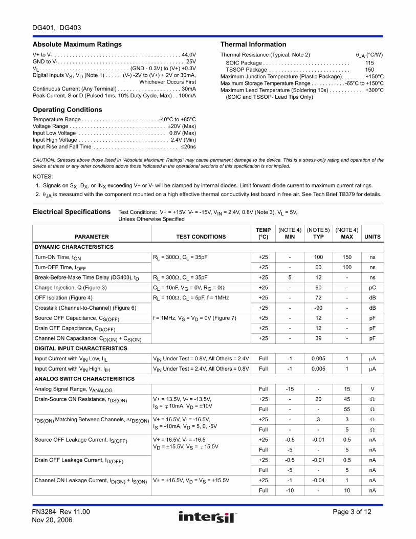
Electrical Specifications Test Conditions: V+ = +15V, V- = -15V, VIN = 2.4V, 0.8V (Note 3), VL = 5V,Unless Otherwise Specified
PARAMETER TEST CONDITIONSTEMP(°C)
(NOTE 4)MIN
(NOTE 5) TYP
(NOTE 4) MAX UNITS
DYNAMIC CHARACTERISTICS
Turn-ON Time, tON RL = 300, CL = 35pF +25 - 100 150 ns
Turn-OFF Time, tOFF +25 - 60 100 ns
Break-Before-Make Time Delay (DG403), tD RL = 300, CL = 35pF +25 5 12 - ns
Charge Injection, Q (Figure 3) CL = 10nF, VG = 0V, RG = 0 +25 - 60 - pC
OFF Isolation (Figure 4) RL = 100, CL = 5pF, f = 1MHz +25 - 72 - dB
Crosstalk (Channel-to-Channel) (Figure 6) +25 - -90 - dB
Source OFF Capacitance, CS(OFF) f = 1MHz, VS = VD = 0V (Figure 7) +25 - 12 - pF
Drain OFF Capacitance, CD(OFF) +25 - 12 - pF
Channel ON Capacitance, CD(ON) + CS(ON) +25 - 39 - pF
DIGITAL INPUT CHARACTERISTICS
Input Current with VIN Low, IIL VIN Under Test = 0.8V, All Others = 2.4V Full -1 0.005 1 A
Input Current with VIN High, IIH VIN Under Test = 2.4V, All Others = 0.8V Full -1 0.005 1 A
ANALOG SWITCH CHARACTERISTICS
Analog Signal Range, VANALOG Full -15 - 15 V
Drain-Source ON Resistance, rDS(ON) V+ = 13.5V, V- = -13.5V, IS = 10mA, VD = 10V
+25 - 20 45
Full - - 55
rDS(ON) Matching Between Channels, rDS(ON) V+ = 16.5V, V- = -16.5V,IS = -10mA, VD = 5, 0, -5V
+25 - 3 3
Full - - 5
Source OFF Leakage Current, IS(OFF) V+ = 16.5V, V- = -16.5VD = 15.5V, VS = 15.5V
+25 -0.5 -0.01 0.5 nA
Full -5 - 5 nA
Drain OFF Leakage Current, ID(OFF) +25 -0.5 -0.01 0.5 nA
Full -5 - 5 nA
Channel ON Leakage Current, ID(ON) + IS(ON) V = 16.5V, VD = VS = 15.5V +25 -1 -0.04 1 nA
Full -10 - 10 nA
FN3284 Rev 11.00 Page 3 of 12Nov 20, 2006
DG401, DG403
POWER SUPPLY CHARACTERISTICS
Positive Supply Current, I+ V+ = 16.5V, V- = -16.5V, VIN = 0V or 5V
+25 - 0.01 1 A
Full - - 5 A
Negative Supply Current, I- +25 -1 -0.01 - A
Full -5 - - A
Logic Supply Current, IL +25 - 0.01 1 A
Full - - 5 A
Ground Current, IGND +25 -1 -0.01 - A
Full -5 - - A
NOTES:
3. VIN = input voltage to perform proper function.
4. The algebraic convention whereby the most negative value is a minimum and the most positive a maximum, is used in this data sheet.
5. Typical values are for DESIGN AID ONLY, not guaranteed nor subject to production testing.
Electrical Specifications Test Conditions: V+ = +15V, V- = -15V, VIN = 2.4V, 0.8V (Note 3), VL = 5V,Unless Otherwise Specified (Continued)
PARAMETER TEST CONDITIONSTEMP(°C)
(NOTE 4)MIN
(NOTE 5) TYP
(NOTE 4) MAX UNITS
Test Circuits and Waveforms
NOTES:
6. Logic input waveform is inverted for switches that have the opposite logic sense.
7. VS = 10V for tON, VS = -10V for tOFF.
FIGURE 1A. MEASUREMENT POINTS
Repeat test for IN2 and S2.For load conditions, see Specifications. CL includes fixture and stray capacitance.
FIGURE 1B. TEST CIRCUIT
FIGURE 1. SWITCHING TIMES
50%
tr < 20nstf < 20ns
tOFF
90%
3V
0V
VS
0V
tON
VO
LOGICINPUT
SWITCHINPUT
SWITCHOUTPUT
90%
-VS
SWITCHINPUT
10%
(NOTE 7)
VO VS
RLRL rDS ON +------------------------------------=
SWITCHINPUT
LOGICINPUT
S1
IN1
V+
D1
RL CL
VO
GND V-
VL
0V -15V
5V +15VRL = 300CL = 35pF
FN3284 Rev 11.00 Page 4 of 12Nov 20, 2006
DG401, DG403
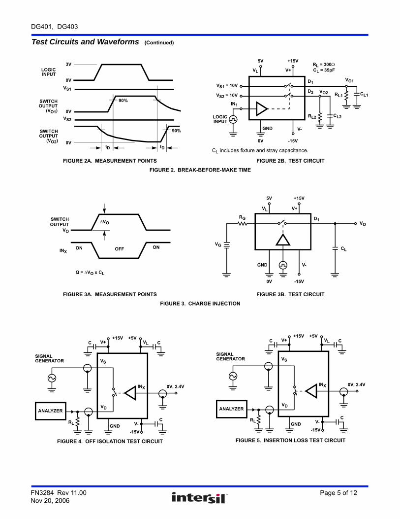
FIGURE 2A. MEASUREMENT POINTS
CL includes fixture and stray capacitance.
FIGURE 2B. TEST CIRCUIT
FIGURE 2. BREAK-BEFORE-MAKE TIME
FIGURE 3A. MEASUREMENT POINTS FIGURE 3B. TEST CIRCUIT
FIGURE 3. CHARGE INJECTION
FIGURE 4. OFF ISOLATION TEST CIRCUIT FIGURE 5. INSERTION LOSS TEST CIRCUIT
Test Circuits and Waveforms (Continued)
90%
3V
0V
tD
0V
LOGICINPUT
SWITCHOUTPUT
SWITCHOUTPUT
VS1
VS2
90%
tD0V
(VO1)
(VO2)
LOGICINPUT
VS1 = 10V
IN1
V+
D1
RL1 CL1
VO1
GND V-
VL
0V -15V
5V +15VRL = 300CL = 35pF
D2
RL2 CL2
VO2VS2 = 10V
VO
VO
INXON OFF ON
Q = VO x CL
SWITCHOUTPUT
V+
D1
CL
VO
V-
RG
VG
VL
0V -15V
5V +15V
GND
ANALYZER
RL
+15V
SIGNALGENERATOR
V+C
V-
-15V
C
0V, 2.4V
VS
VD
INX
GND
+5VVL C
ANALYZER
RL
+15V
SIGNALGENERATOR
V+C
V-
-15V
C
0V, 2.4V
VS
VD
INX
GND
+5VVL C
FN3284 Rev 11.00 Page 5 of 12Nov 20, 2006
DG401, DG403
Application Information
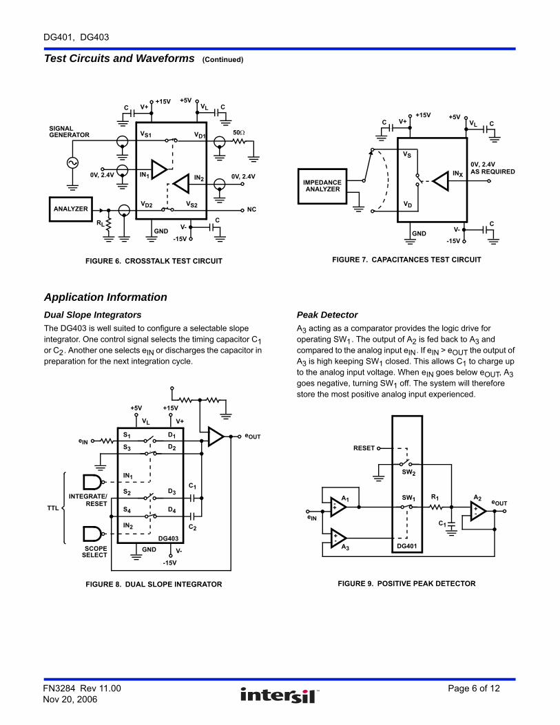
Dual Slope Integrators
The DG403 is well suited to configure a selectable slope integrator. One control signal selects the timing capacitor C1 or C2. Another one selects eIN or discharges the capacitor in preparation for the next integration cycle.
Peak Detector
A3 acting as a comparator provides the logic drive for operating SW1. The output of A2 is fed back to A3 and compared to the analog input eIN. If eIN > eOUT the output of A3 is high keeping SW1 closed. This allows C1 to charge up to the analog input voltage. When eIN goes below eOUT, A3 goes negative, turning SW1 off. The system will therefore store the most positive analog input experienced.
FIGURE 6. CROSSTALK TEST CIRCUIT FIGURE 7. CAPACITANCES TEST CIRCUIT
Test Circuits and Waveforms (Continued)
0V, 2.4V
ANALYZER
+15VV+C
VS1SIGNALGENERATOR
RLGND
IN1
VD1
IN2
50
0V, 2.4V
NC
V-
-15V
C
VD2
+5VVL C
VS2
+15VV+C
GND
VS
VD
INX
V-
-15V
C
IMPEDANCEANALYZER
0V, 2.4V
+5VVL C
AS REQUIRED
V-GND
-15V
IN2
IN1
S3
S1
S2
S4
D1
D2
D3
D4
+15V+5V
VL V+
DG403
C1
C2
eOUTeIN
INTEGRATE/
SCOPE
TTLRESET
SELECT
FIGURE 8. DUAL SLOPE INTEGRATOR
eOUT
eINC1
R1
SW2
SW1
RESET
+-
+-
+-
DG401
A1
A3
FIGURE 9. POSITIVE PEAK DETECTOR
A2
FN3284 Rev 11.00 Page 6 of 12Nov 20, 2006
DG401, DG403
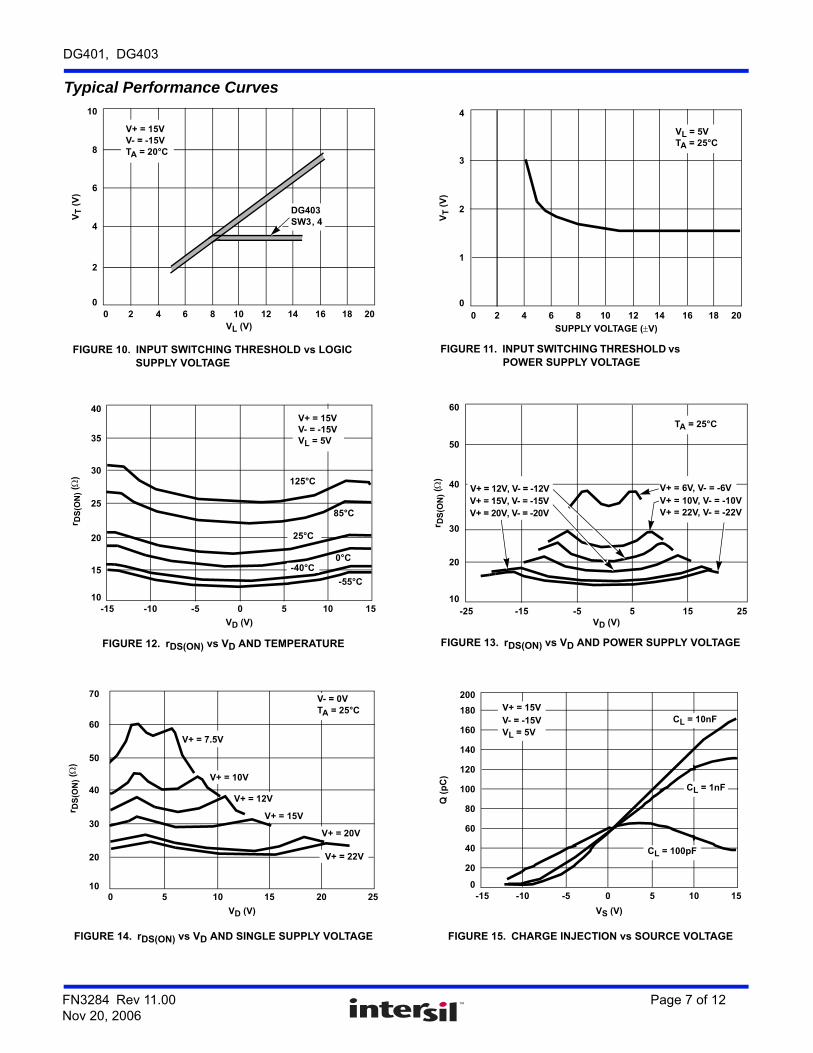
Typical Performance Curves
FIGURE 10. INPUT SWITCHING THRESHOLD vs LOGICSUPPLY VOLTAGE
FIGURE 11. INPUT SWITCHING THRESHOLD vs POWER SUPPLY VOLTAGE
FIGURE 12. rDS(ON) vs VD AND TEMPERATURE FIGURE 13. rDS(ON) vs VD AND POWER SUPPLY VOLTAGE
FIGURE 14. rDS(ON) vs VD AND SINGLE SUPPLY VOLTAGE FIGURE 15. CHARGE INJECTION vs SOURCE VOLTAGE
VT (
V)
VL (V)
10
8
6
4
2
00 2 4 6 8 10 12 14 16 18 20
V+ = 15VV- = -15VTA = 20°C
DG403SW3, 4 V
T (
V)
SUPPLY VOLTAGE (V)
4
3
2
1
00 2 4 6 8 10 12 14 16 18 20
VL = 5VTA = 25°C
0°C
r DS
(ON
) (
)
VD (V)
40
35
30
25
20
15
10-15 -10 -5 0 5 10 15
V+ = 15VV- = -15VVL = 5V
25°C
125°C
85°C
-40°C
-55°C
r DS
(ON
) (
)
VD (V)-15-25 -5 5 2515
60
50
40
30
20
10
TA = 25°C
V+ = 6V, V- = -6VV+ = 10V, V- = -10VV+ = 22V, V- = -22V
V+ = 12V, V- = -12VV+ = 15V, V- = -15VV+ = 20V, V- = -20V
r DS
(ON
) (
)
VD (V)
50 10 15 2520
60
50
40
30
20
10
70
V+ = 7.5V
V+ = 10V
V+ = 15V
TA = 25°C
V+ = 20V
V+ = 22V
V+ = 12V
V- = 0V
Q (
pC
)
VS (V)
200
180
160
140
120
100
80
60
40
20
0-15 -10 -5 5 10 15
V+ = 15V
V- = -15VVL = 5V
CL = 1nF
0
CL = 10nF
CL = 100pF
FN3284 Rev 11.00 Page 7 of 12Nov 20, 2006
DG401, DG403
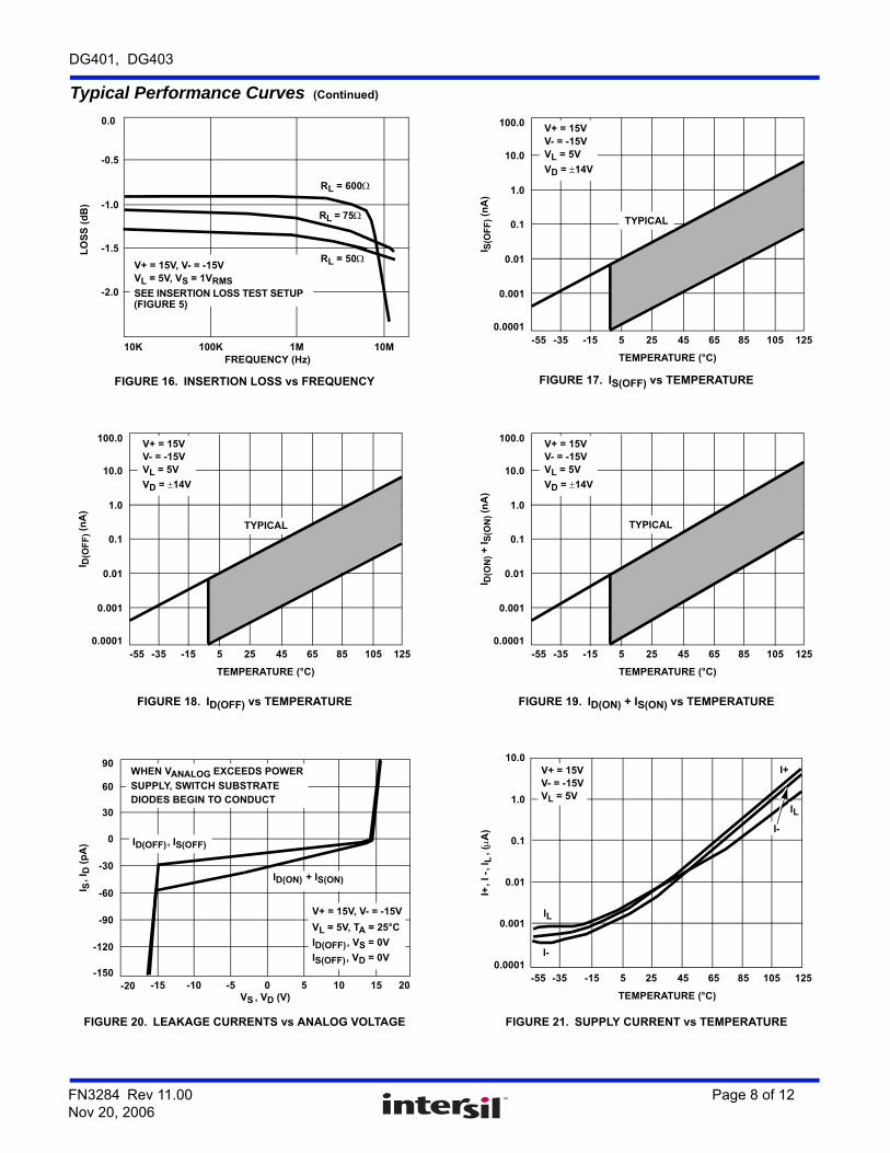
FIGURE 16. INSERTION LOSS vs FREQUENCY FIGURE 17. IS(OFF) vs TEMPERATURE
FIGURE 18. ID(OFF) vs TEMPERATURE FIGURE 19. ID(ON) + IS(ON) vs TEMPERATURE
FIGURE 20. LEAKAGE CURRENTS vs ANALOG VOLTAGE FIGURE 21. SUPPLY CURRENT vs TEMPERATURE
Typical Performance Curves (Continued)
FREQUENCY (Hz)
LO
SS
(d
B)
0.0
-0.5
-1.0
-1.5
-2.0
10K 100K 1M 10M
RL = 600
RL = 75
RL = 50V+ = 15V, V- = -15VVL = 5V, VS = 1VRMSSEE INSERTION LOSS TEST SETUP(FIGURE 5)
TEMPERATURE (°C)
-55 -35 -15 5 25 45 65
I S(O
FF
) (n
A)
85 105 125
100.0
10.0
1.0
0.1
0.01
0.001
0.0001
V+ = 15VV- = -15VVL = 5V
VD = 14V
TYPICAL
TEMPERATURE (°C)
-55 -35 -15 5 25 45 65
I D(O
FF
) (n
A)
85 105 125
100.0
10.0
1.0
0.1
0.01
0.001
0.0001
V+ = 15VV- = -15VVL = 5V
VD = 14V
TYPICAL
TEMPERATURE (°C)
-55 -35 -15 5 25 45 65
I D(O
N)
+ I
S(O
N) (n
A)
85 105 125
100.0
10.0
1.0
0.1
0.01
0.001
0.0001
V+ = 15VV- = -15VVL = 5V
VD = 14V
TYPICAL
90
60
30
0
-30
-90
-150-15 -10 -5 0 5 10 15
VS , VD (V)
I S, I
D (
pA
)
-20 20
-120
-60
V+ = 15V, V- = -15V
VL = 5V, TA = 25°C
ID(OFF), VS = 0V
IS(OFF), VD = 0V
ID(ON) + IS(ON)
ID(OFF), IS(OFF)
WHEN VANALOG EXCEEDS POWER
SUPPLY, SWITCH SUBSTRATE DIODES BEGIN TO CONDUCT
IL
I+, I
-, I
L,
(A
)
TEMPERATURE (°C)
-55 -35 -15 5 25 45 65 85 105 125
10.0
1.0
0.1
0.01
0.001
0.0001
V+ = 15VV- = -15VVL = 5V
I-
I+
IL
I-
FN3284 Rev 11.00 Page 8 of 12Nov 20, 2006
DG401, DG403
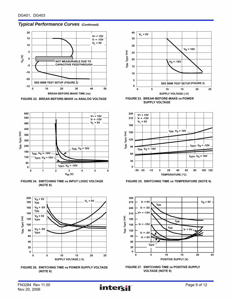
FIGURE 22. BREAK-BEFORE-MAKE vs ANALOG VOLTAGE FIGURE 23. BREAK-BEFORE-MAKE vs POWER SUPPLY VOLTAGE
FIGURE 24. SWITCHING TIME vs INPUT LOGIC VOLTAGE (NOTE 8)
FIGURE 25. SWITCHING TIME vs TEMPERATURE (NOTE 8)
FIGURE 26. SWITCHING TIME vs POWER SUPPLY VOLTAGE (NOTE 8)
FIGURE 27. SWITCHING TIME vs POSITIVE SUPPLY VOLTAGE (NOTE 8)
Typical Performance Curves (Continued)
BREAK-BEFORE-MAKE TIME (ns)
-15
-10
-5
0
5
10
15
-20
20
VS
(V
)
0 5040302010
NOT MEASURABLE DUE TOCAPACITIVE FEEDTHROUGH
SEE BBM TEST SETUP
V+ = 15VV- = -15VVL = 5V
(FIGURE 2)
SUPPLY VOLTAGE (V)
5
10
15
20
25
30
35
0
40
0 252015105
t ON
, tO
FF (
ns
)
SEE BBM TEST SETUP
VS = 10V
VS = -10V
VL = 5V
(FIGURE 2)
VIN (V)
60
120
180
240
300
360
420
0
480
0 54321
t ON
, tO
FF (
ns
)
6
540
600
VL = 5V
V+ = 15VV- = -15V
tON, VS = 10V
tOFF, VS = -10V
tOFF, VS = 10V
tON, VS = -10V
TEMPERATURE (°C)
-55 -35 -15 5 25 45 65 85 105 125
180
150
120
90
60
30
0
t ON
, tO
FF (
ns
)
210
240
VL = 5V
V+ = 15VV- = -15V
tON, VS = 10V
tON, VS = -10VtOFF, VS = -10V
tOFF, VS = 10V
SUPPLY VOLTAGE (V)
0 252015105
120
100
80
60
40
20
0
t ON
, t O
FF (
ns)
140
160
180
200VL = 5V
VS = -5V
VS = -5V
tON
tOFF
tOFF VS = 5V
tON VS = 5V
180
150
120
90
60
30
0
t ON
, t O
FF (
ns
)
210
240
POSITIVE SUPPLY (V)
0 252015105
270
300
V- = -15
V- = 0V
V- = -5V
V- = -15V
V- = -5VV- = 0V
VS = 5VtON
tON
tON
tOFF
V- = 0V
V+ = -15V
FN3284 Rev 11.00 Page 9 of 12Nov 20, 2006
DG401, DG403
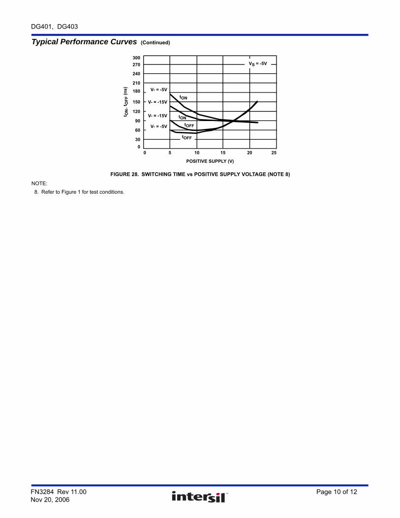
FIGURE 28. SWITCHING TIME vs POSITIVE SUPPLY VOLTAGE (NOTE 8)
NOTE:
8. Refer to Figure 1 for test conditions.
Typical Performance Curves (Continued)
180
150
120
90
60
30
0
t ON
, tO
FF (
ns
)
210
240
POSITIVE SUPPLY (V)
0 252015105
270
300VS = -5V
tON
tON
tOFF
V- = -15V
V- = -5V
V- = -15V
V- = -5V
tOFF
FN3284 Rev 11.00 Page 10 of 12Nov 20, 2006
DG401, DG403
FN3284 Rev 11.00 Page 11 of 12Nov 20, 2006
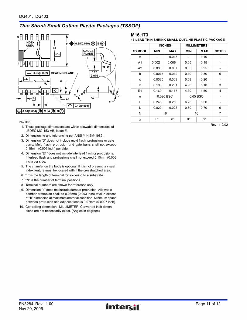
Thin Shrink Small Outline Plastic Packages (TSSOP)
NOTES:
1. These package dimensions are within allowable dimensions of JEDEC MO-153-AB, Issue E.
2. Dimensioning and tolerancing per ANSI Y14.5M-1982.
3. Dimension “D” does not include mold flash, protrusions or gate burrs. Mold flash, protrusion and gate burrs shall not exceed0.15mm (0.006 inch) per side.
4. Dimension “E1” does not include interlead flash or protrusions. Interlead flash and protrusions shall not exceed 0.15mm (0.006inch) per side.
5. The chamfer on the body is optional. If it is not present, a visual index feature must be located within the crosshatched area.
6. “L” is the length of terminal for soldering to a substrate.
7. “N” is the number of terminal positions.
8. Terminal numbers are shown for reference only.
9. Dimension “b” does not include dambar protrusion. Allowable dambar protrusion shall be 0.08mm (0.003 inch) total in excessof “b” dimension at maximum material condition. Minimum spacebetween protrusion and adjacent lead is 0.07mm (0.0027 inch).
10. Controlling dimension: MILLIMETER. Converted inch dimen-sions are not necessarily exact. (Angles in degrees)
INDEXAREA
E1
D
N
1 2 3
-B-
0.10(0.004) C AM B S
e
-A-
b
M
-C-
A1
A
SEATING PLANE
0.10(0.004)
c
E 0.25(0.010) BM M
L0.25
0.010
GAUGEPLANE
A2
0.05(0.002)
M16.17316 LEAD THIN SHRINK SMALL OUTLINE PLASTIC PACKAGE
SYMBOL
INCHES MILLIMETERS
NOTESMIN MAX MIN MAX
A - 0.043 - 1.10 -
A1 0.002 0.006 0.05 0.15 -
A2 0.033 0.037 0.85 0.95 -
b 0.0075 0.012 0.19 0.30 9
c 0.0035 0.008 0.09 0.20 -
D 0.193 0.201 4.90 5.10 3
E1 0.169 0.177 4.30 4.50 4
e 0.026 BSC 0.65 BSC -
E 0.246 0.256 6.25 6.50 -
L 0.020 0.028 0.50 0.70 6
N 16 16 7
0° 8° 0° 8° -
Rev. 1 2/02
FN3284 Rev 11.00 Page 12 of 12Nov 20, 2006
DG401, DG403
Intersil products are manufactured, assembled and tested utilizing ISO9001 quality systems as notedin the quality certifications found at www.intersil.com/en/support/qualandreliability.html
Intersil products are sold by description only. Intersil may modify the circuit design and/or specifications of products at any time without notice, provided that such modification does not, in Intersil's sole judgment, affect the form, fit or function of the product. Accordingly, the reader is cautioned to verify that datasheets are current before placing orders. Information furnished by Intersil is believed to be accurate and reliable. However, no responsibility is assumed by Intersil or its subsidiaries for its use; nor for any infringements of patents or other rights of third parties which may result from its use. No license is granted by implication or otherwise under any patent or patent rights of Intersil or its subsidiaries.
For information regarding Intersil Corporation and its products, see www.intersil.com
For additional products, see www.intersil.com/en/products.html
© Copyright Intersil Americas LLC 1999-2006. All Rights Reserved.All trademarks and registered trademarks are the property of their respective owners.
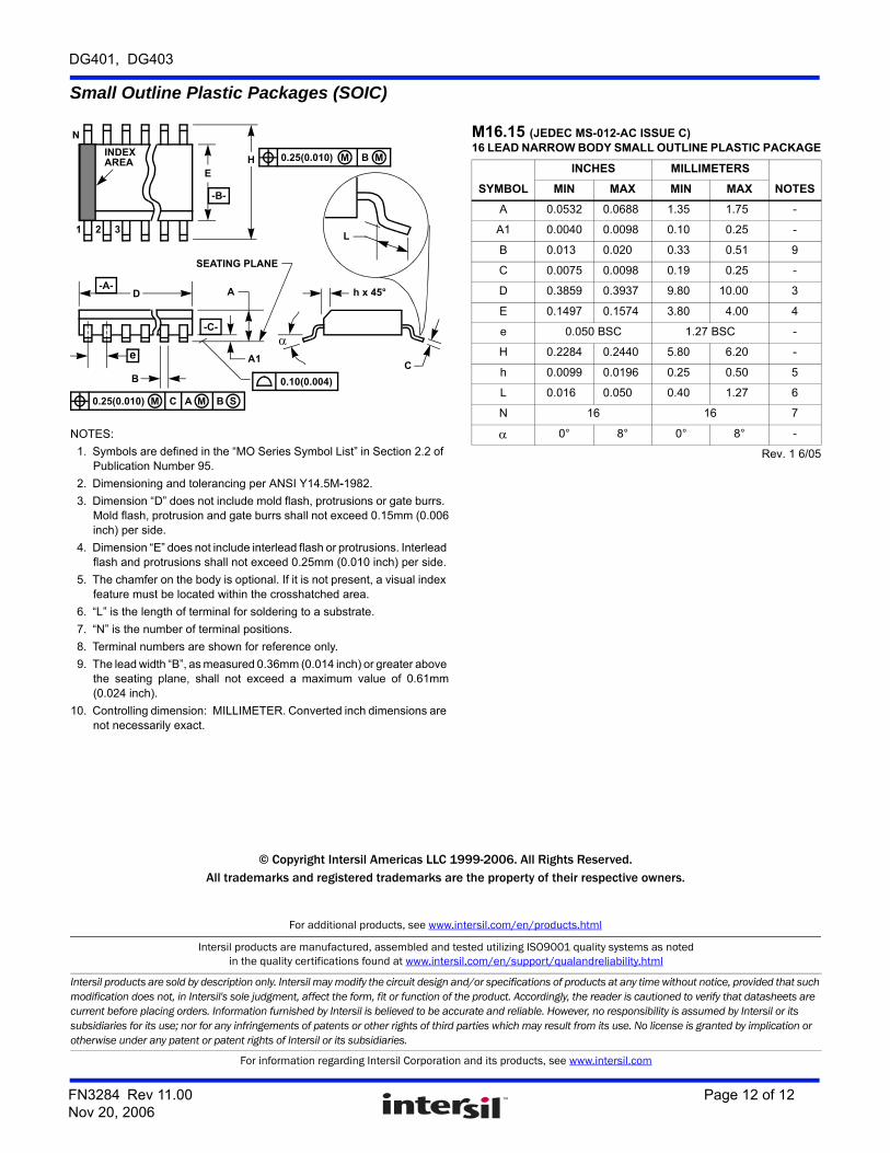
Small Outline Plastic Packages (SOIC)
NOTES:
1. Symbols are defined in the “MO Series Symbol List” in Section 2.2 of Publication Number 95.
2. Dimensioning and tolerancing per ANSI Y14.5M-1982.
3. Dimension “D” does not include mold flash, protrusions or gate burrs. Mold flash, protrusion and gate burrs shall not exceed 0.15mm (0.006inch) per side.
4. Dimension “E” does not include interlead flash or protrusions. Interlead flash and protrusions shall not exceed 0.25mm (0.010 inch) per side.
5. The chamfer on the body is optional. If it is not present, a visual index feature must be located within the crosshatched area.
6. “L” is the length of terminal for soldering to a substrate.
7. “N” is the number of terminal positions.
8. Terminal numbers are shown for reference only.
9. The lead width “B”, as measured 0.36mm (0.014 inch) or greater above the seating plane, shall not exceed a maximum value of 0.61mm(0.024 inch).
10. Controlling dimension: MILLIMETER. Converted inch dimensions are not necessarily exact.
INDEXAREA
E
D
N
1 2 3
-B-
0.25(0.010) C AM B S
e
-A-
L
B
M
-C-
A1
A
SEATING PLANE
0.10(0.004)
h x 45°
C
H 0.25(0.010) BM M
M16.15 (JEDEC MS-012-AC ISSUE C)16 LEAD NARROW BODY SMALL OUTLINE PLASTIC PACKAGE
SYMBOL
INCHES MILLIMETERS
NOTESMIN MAX MIN MAX
A 0.0532 0.0688 1.35 1.75 -
A1 0.0040 0.0098 0.10 0.25 -
B 0.013 0.020 0.33 0.51 9
C 0.0075 0.0098 0.19 0.25 -
D 0.3859 0.3937 9.80 10.00 3
E 0.1497 0.1574 3.80 4.00 4
e 0.050 BSC 1.27 BSC -
H 0.2284 0.2440 5.80 6.20 -
h 0.0099 0.0196 0.25 0.50 5
L 0.016 0.050 0.40 1.27 6
N 16 16 7
0° 8° 0° 8° -
Rev. 1 6/05