Embed Size (px)
Citation preview

ii
DIABETIC FOOT DETECTOR
By
MOHD HANAFI MUSTAFFA
FINAL PROJECT REPORT
Submitted to the Electrical & Electronics Engineering Programme
in Partial Fulfillment of the Requirements
for the Degree
Bachelor of Engineering (Hons) (Electrical & Electronics Engineering)
Universiti Teknologi Petronas
Bandar Seri Iskandar
31750 Tronoh
Perak Darul Ridzuan
Copyright 2010
by
Mohd Hanafi bin Mustaffa, 2010

iii
CERTIFICATION OF APPROVAL
DIABETIC FOOT DETECTOR
by
Mohd Hanafi bin Mustaffa
A project dissertation submitted to the
Electrical & Electronics Engineering Programme
Universiti Teknologi PETRONAS
in partial fulfilment of the requirement for the
Bachelor of Engineering (Hons)
(Electrical & Electronics Engineering)
Approved:
__________________________
Ms. Salina Mohmad
Project Supervisor
UNIVERSITI TEKNOLOGI PETRONAS
TRONOH, PERAK
December 2010

iv
CERTIFICATION OF ORIGINALITY
This is to certify that I am responsible for the work submitted in this project, that the
original work is my own except as specified in the references and acknowledgements,
and that the original work contained herein have not been undertaken or done by
unspecified sources or persons.
__________________________
Mohd Hanafi bin Mustaffa

v
ABSTRACT
Diabetic foot detector is a device use to detect human foot pressure especially
for diabetic patient. The abnormality of the foot pressure is an early indication of the
diabetic foot. Diabetic patient with this symptom cannot control the pressure applied
to the feet resulting tissue injury to the foot even for a short distance walking. The
most common cases occur in the peak plantar surfaces since the transfer of high peak
pressure from heel area to the forefoot area. The data acquisition device embedded to
the shoe sole to collect real time foot pressure. This data acquisition system is
constructed using force sensor and negative feedback circuit. The pressure of the foot
is detected using the force sensor which uses resistance to represent the foot pressure
as the detection system. The voltage from the negative feedback output is then sent to
the microprocessor using radio frequency transmission to convert it to the real value
before the data is transferred to the user interface.

vi
ACKNOWLEDGEMENTS
First of all, there were many people, individuals and parties that involved while working for my final year project which has contributed immeasurable and invaluable amount of help, guidance, assistance, advice, supports, and also supervision.
Special thanks to Miss Salina Mohmad, my final year project supervisor for her support and guidance. I also like to say thank you again to her for given me many supportive, constructive advices, and sharing her technical knowledge. Without her guidance, the project cannot be completed.

vii
TABLE OF CONTENTS
LIST OF TABLES ....................................................................................................... ix
LIST OF FIGURES ...................................................................................................... x
CHAPTER 1 INTRODUCTION .................................................................................. 1
1.1 Background of study ........................................................................ 1
1.2 Problem Statement ........................................................................... 2
1.3 Objective .......................................................................................... 3
1.4 Scope of study .................................................................................. 3
CHAPTER 2 LITERATURE REVIEW ....................................................................... 4
2.1 Diabetic Foot .................................................................................... 4
2.2 Force Sensor ..................................................................................... 5
2.3 Microcontroller ................................................................................. 6
2.4 Radio Frequency Transmission ........................................................ 7
2.5 Liquid Crystal Display ..................................................................... 9
2.6 Diabetic Foot Detector ................................................................... 10
CHAPTER 3 METHODOLOGY ............................................................................... 11
3.1 Procedure Identification ................................................................. 11
3.2 Pressure Sensor Testing ................................................................. 12
3.3 Sensor Circuit Simulation .............................................................. 13
3.4 Sensor Circuit Testing .................................................................... 14
3.5 Microcontroller Programming ........................................................ 15
3.6 Product Testing .............................................................................. 16
3.7 Project Flow ................................................................................... 18
CHAPTER 4 RESULT AND DISCUSSION ............................................................. 19
4.1 Foce Sensor Analysis ..................................................................... 19
4.2 Sensor Circuit Simulation .............................................................. 21
4.2.1 Sensor Circuit Simulation for Sensor A ................................ 21
4.2.2 Sensor Circuit Simulation for Sensor B ................................. 22
4.2.3 Sensor Circuit Simulation for Sensor C ................................. 24
4.2.3 Sensor Circuit Simulation Analysis ....................................... 25
4.3 Sensor Circuit Testing .................................................................... 26
4.4 Transmitter Circuit ......................................................................... 28

viii
4.5 Receiver Circuit .............................................................................. 29
4.6 Data Acquisition Design ................................................................ 30
4.7 Source Code ................................................................................... 31
CHAPTER 5 CONCLUSION AND RECOMMENDATION .................................... 32
5.1 Conclusion ...................................................................................... 32
5.2 Recommendation ............................................................................ 32
REFERENCE .............................................................................................................. 33
APPENDICES ............................................................................................................ 34
APPENDIX A PROGRAMMING SOURCE CODE .......................... 35
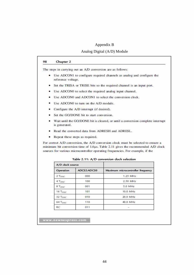
APPENDIX B ANALOG DIGITAL MODULE ................................. 39

ix
LIST OF TABLES
Table 1 16x2 Liquid Crystal Display Pin Descriptions ............................................... 9
Table 2 Resistance for difference mass ...................................................................... 19
Table 3 Voltage for difference resistance (Sensor A) ................................................ 21
Table 4 Voltage for difference resistance (Sensor B) ................................................ 22
Table 5 Voltage for difference resistance (Sensor C) ................................................ 24
Table 6 Output voltage for sensor circuit testing ....................................................... 26

x
LIST OF FIGURES
Figure 1 The usage of 5.07/10g Semmes-Weinstein monofilament ............................ 2
Figure 2 Frequent sites of loss of sensation ................................................................. 4
Figure 3 Ulcers formation on diabetic foot patients..................................................... 4
Figure 4 Force Sensor .................................................................................................. 5
Figure 5 Sites for sensors placement ............................................................................ 5
Figure 6 PIC18F452 microcontroller DIP pin configuration ....................................... 6
Figure 7 Connection between the Microcontroller and the user interface ................... 7
Figure 8 RTF Block Diagram ...................................................................................... 8
Figure 9 RRF Block Diagram ...................................................................................... 8
Figure 10 16x2 Liquid Crystal Display (LCD) ............................................................ 9
Figure 11 Diabetic foot detector ................................................................................ 10
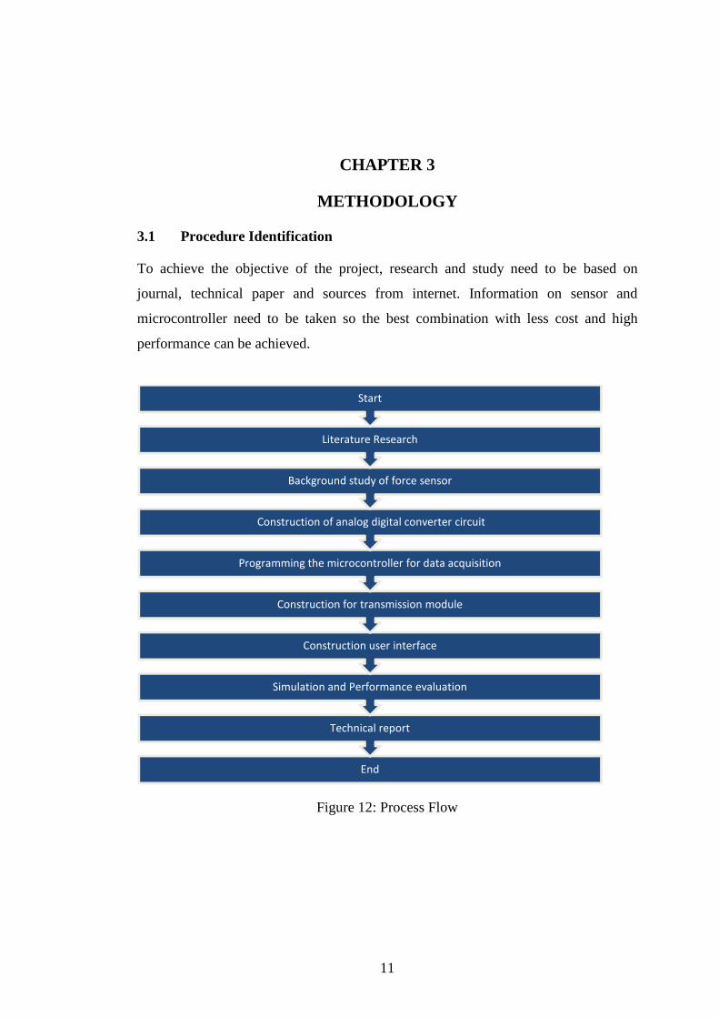
Figure 12 Process Flow .............................................................................................. 11
Figure 13 Mass is applied to the pressure sensor and the sensor testing ................... 12
Figure 14 The resistance reading before the mass is applied and maximum mass .... 12
Figure 15 Simulation sensor circuit ........................................................................... 13
Figure 16 Simulation result for Sensor A (123.3 kΩ) ................................................ 13
Figure 17 Sensor circuit ............................................................................................. 14
Figure 18 Maximum voltage of the circuit reading ................................................... 14
Figure 19 Programming Flow Chart .......................................................................... 15
Figure 20 MikroC C compiler integrated development environment (IDE) ............. 15
Figure 21 Sensor testing ............................................................................................. 16
Figure 22 Data transmission testing ........................................................................... 16
Figure 23 Microcontroller testing .............................................................................. 17
Figure 24 Project flow ................................................................................................ 18
Figure 25 Resistance vs Mass .................................................................................... 20
Figure 26 Vout vs Resistance for Sensor A ............................................................... 22
Figure 27 Vout vs Resistance for Sensor B ................................................................. 23
Figure 28 Vout vs Resistance for Sensor C ................................................................. 25
Figure 29 Vout vs Resistance for Sensor A,B and C .................................................. 25
Figure 30 Vout vs Resistance ...................................................................................... 27
Figure 31 Vout vs Resistance for 1.5kΩ to 92.9kΩ .................................................. 27

xi
Figure 32 Schematic transmitter circuit ..................................................................... 28
Figure 33 Transmitter board layout design ................................................................ 28
Figure 34 Schematic of the receiver circuit ............................................................... 29
Figure 35 Receiver board layout design..................................................................... 30
Figure 36 Site for sensor placement ........................................................................... 30
Figure 37 Sensor placement on shoe sole and in the shoe ......................................... 30
Figure 38 Sensor placement on 1st and 2nd metatarsals and heel ............................. 31

1
CHAPTER 1
INTRODUCTION
1.1 Background of study
The foot pathology (diabetic foot) is the common diabetic complication that
requires the patient to be hospitalized. The total cost of the diabetic foot in the United
State alone is estimated to approach $4 billion annually mostly on ulcer care and
amputations [2,3]. It is presume that the increase in the body weight and the diabetes
lead to increment of the pressure to the foot peak plantar [2,3]. The high foot peak
plantar and incapable to control the applied to the foot pressure due to the neuropathy
(peripheral sensory neuropathy & autonomic and motor neuropathy) causes the
development of the foot ulceration [2,3]. The wound cannot be healed in the normal
way and the diabetic ulcer will stay in the inflammatory stage of wound repair [2,3].
The abnormal foot pressure can be one of the factors leading to the diabetic foot [2,3].
This project aims to collect the data of the foot pressure of the diabetic patient to
monitor any abnormality that can cause diabetic foot to occur [2,3].

2
1.2 Problem statement
Diabetes mellitus is a disease due to the high blood sugar (glucose) levels.
This high blood sugar (glucose) levels are because of defect in insulin secretion or
insulin action or both. Insulin is a hormone that occur is produced in the pancreas,
used to control the blood glucose level in the blood [2,3]. For normal person,
pancreas will release the insulin to the blood when the blood glucose level is high in
order to compensate it. Diabetic can be controlled but it lasts a lifetime [2,3]. One of
the major complications of the diabetes is the diabetic foot ulceration (foot pathology)
[2,3]. This occurs when the feet become pain insensitivity and the development of the
trauma to the feet (high pressure to the feet during walking). Since the patient with
diabetes has impaired wound healing, this complication will lead to the development
of chronic ulceration and amputation of the lower extremity [2,3]. One method to
detect loss of sensation is using the 5.07/10g Semmes-Weinstein monofilament but it
requires the patient to be hospitalized and costly since the treatment can only be done
by the neurologist. The most frequent sites of loss of sensation are:
i. Heel
ii. Second metatarsal
iii. Dorsum of the little toe
iv. The head of the first and third metatarsal
Figure 1: The usage of 5.07/10g Semmes-Weinstein monofilament [12]

3
1.3 Objective
The objectives for this project are:
1. To construct the data acquisition for the foot pressure in the real time by
interface the pressure sensor with the microcontroller.
2. To create the communication between data acquisition module and the user
interface using the radio transmission.
3. To develop the interface to monitor the foot pressure for the monitoring
purpose.
4. To develop interface between the microcontroller and the user using liquid
crystal display.
1.4 Scope of study
This project focuses on the data acquisition of the foot pressure in the real time. The
data is collected by the pressure sensor. The process for data acquisition is done using
pressure sensor and the data is process using microprocessor into the digital data.
Then, the data is transmitted to the receiver using the radio frequency. These sensors
are located at high pressure areas over heel, metatarsal heads and hallux of each foot.
The propose placement of the sensors are at heel and the all five metatarsal heads.
The sensor will be connected to the radio frequency module to make wireless
connection between microprocessor. The microprocessor at data acquisition module
will be programmed to interpret the data into the digital form and display on user
interface. The data collected can be analyzed to determine test subject is having
peripheral neuropathy. This will help to analyzed the diabetic patient quickly and
more accurate.

4
CHAPTER 2
LITERATURE REVIEW
2.1 Diabetic foot
The sensory neuropathy associated with pain insensitivity is the first
indication of the diabetic foot. The existence of trauma is plantar tissue stress and
injury that result from the development of high foot pressure during walking cause
the development of ulceration. The impaired wound healing and reduced blood flow
in the ulcer area prevent wound healing lead to chronic ulceration and sometimes
amputation [2,3]. Figure 2 shows the most frequent sites of loss of sensation are.
Figure 2: Frequent sites of loss of sensation [13]
Figure 3 show the formation of ulcers on first and second metatarsal head on diabetic
foot patients.
Figure 3: Ulcers formation on diabetic foot patients [14]
The preventions actions for those who are prone to have diabetic foot are [15]:
i. Good diabetes control by controlling the insulin levelin blood.
ii. Regular leg and foot self-examinations to detect any trauma on foot.
iii. Obtain knowledge on how to recognize problems related to the diabetic
foot

5
iv. Choose proper footwear with a high and wide toe box to prevent chafing
and pinching that can harm the toes. The shoe should protect the feet from
blisters, bleedings and lesions.
v. Regular exercise.
vi. Avoid injury by keeping footpaths clear.
These prevention actions only reduce the chance for the diabetic patients to have
diabetic foot. Monitoring patient foot pressure is a better solution where the medical
practitioner able to monitor any abnormality of foot pressure.
2.2 Force Sensor
The force sensor acts as a force sensing (foot pressure) resistor in an electrical
circuit. The resistance will determine the force applied to the sensor. When there is no
force applied on the sensor, the resistance is very high (close to open circuit) and the
resistance value is decreased when the force is applied [4]. In this project the pressure
sensor is customized using the conductive sponge and conductive material. The
layout of the sensor is shown in Figure 4.
Figure 4: Force Sensor
Figure 5: Sites for sensors placement [13]
6
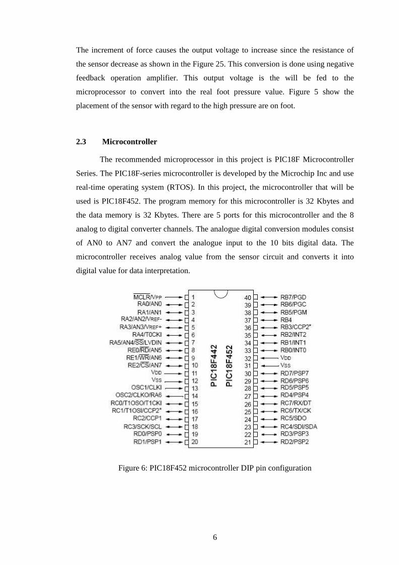
The increment of force causes the output voltage to increase since the resistance of
the sensor decrease as shown in the Figure 25. This conversion is done using negative
feedback operation amplifier. This output voltage is the will be fed to the
microprocessor to convert into the real foot pressure value. Figure 5 show the
placement of the sensor with regard to the high pressure are on foot.
2.3 Microcontroller
The recommended microprocessor in this project is PIC18F Microcontroller
Series. The PIC18F-series microcontroller is developed by the Microchip Inc and use
real-time operating system (RTOS). In this project, the microcontroller that will be
used is PIC18F452. The program memory for this microcontroller is 32 Kbytes and
the data memory is 32 Kbytes. There are 5 ports for this microcontroller and the 8
analog to digital converter channels. The analogue digital conversion modules consist
of AN0 to AN7 and convert the analogue input to the 10 bits digital data. The
microcontroller receives analog value from the sensor circuit and converts it into
digital value for data interpretation.
Figure 6: PIC18F452 microcontroller DIP pin configuration

7
Figure 7: Connection between the Microcontroller and the user interface
Figure 7 show the connection between microcontroller and the user interface using
liquid crystal display. Pressure sensor consists of pressure sensor and sensor circuit
(negative feedback amplifier circuit) will send analog data in voltage ranging from 0
V to 5 V. The analogue digital converter of the microcontroller will convert the
analog data to digital data into 10 bits digital data. These data will be converted into
mass applied to the foot using the equations obtain from the graph resistance vs. mass
and resistance vs. output voltage. The result of the conversion will be sent to the
liquid crystal display (LCD) using The American Standard Code for Information
Interchange (ASCII) format.
2.4 Radio Frequency (RF) Transmission
The wireless transmission in this project is done using radio frequency (RF)
transmission. The transmitter that will be used is FSK Radio Transmitter with Crystal
Oscillator (FM-RTFQ1-433) and the receiver that will be used is FSK Superhet
Receiver with Crystal Oscillator (RRFQ1-433) [10]. The working frequency for this
module is the 433.92 MHz [10]. FM Radio Transmitter & Receivers specifications
are:
1. Transmission range up to 250 m[10].
2. The data link for this module is upto 40 Kbit/s at distances 75 metres in-building
and 300 metres open ground[10].

8
The sizes of both modules are small to make sure it is mobile and do not constraint
the user. The power dissipation for the transmitter is very low about 6.8mA for while
operate and 100nA while standby [10]. This is important since the transmitter module
is mobile. The range of the transmission can be increase by using multi node wireless
link.
Figure 8: RTF Block Diagram
Figure 9: RRF Block Diagram

9
2.5 Liquid Crystal Display (LCD)
The display chose in this project is the HD44780U dot-matrix liquid crystal display
controller and driver LSI displays alphanumeric. A single HD44780U can display up
to one 8-character line or two 8-character lines. This display use low power supply
(2.7V to 5.5V)
Figure 10: 16x2 Liquid Crystal Display (LCD)
Table 1: 16x2 Liquid Crystal Display Pin Descriptions
Pin No. Name Description
1 Vss Ground
2 Vdd Positive Supply
3 Vee Contrast
4 RS Register Select
5 R/W Read/Write
6 E Enable
7 D0 Data bit 0
8 D1 Data bit 1
9 D2 Data bit 2
10 D3 Data bit 3
11 D4 Data bit 4
12 D5 Data bit 5
13 D6 Data bit 6
14 D7 Data bit 7

The function if each connection is shown in table 1. Pin 7 to 14 are the eight data bus
lines (D0 to D7). Data can be transferred to and from the display, either as a single 8
bit byte or as two 4-bit “nibble”. In this project only the upper four data line
D7) is used.
2.6 Diabetic foot detector
The data acquisition module consists of three main components. The first
component is the force sensor. The function of the force sensor is to measure the
force applied to the foot.
for transmission purpose. The receiver will accept the data and send the data to the
microcontroller. The microcontroller will convert the data into the real value and send
to the user interface.
10
The function if each connection is shown in table 1. Pin 7 to 14 are the eight data bus
lines (D0 to D7). Data can be transferred to and from the display, either as a single 8
bit “nibble”. In this project only the upper four data line
foot detector
Figure 11: Diabetic foot detector
he data acquisition module consists of three main components. The first
component is the force sensor. The function of the force sensor is to measure the
to the foot. The output of the sensor will be connected to the transmitter
for transmission purpose. The receiver will accept the data and send the data to the
microcontroller. The microcontroller will convert the data into the real value and send
User Interface
Microcontroller
Transmission module
Data acquisition module
The function if each connection is shown in table 1. Pin 7 to 14 are the eight data bus
lines (D0 to D7). Data can be transferred to and from the display, either as a single 8-
bit “nibble”. In this project only the upper four data line (D4 to
he data acquisition module consists of three main components. The first
component is the force sensor. The function of the force sensor is to measure the
The output of the sensor will be connected to the transmitter
for transmission purpose. The receiver will accept the data and send the data to the
microcontroller. The microcontroller will convert the data into the real value and send
11
CHAPTER 3
METHODOLOGY
3.1 Procedure Identification
To achieve the objective of the project, research and study need to be based on
journal, technical paper and sources from internet. Information on sensor and
microcontroller need to be taken so the best combination with less cost and high
performance can be achieved.
Figure 12: Process Flow
End
Technical report
Simulation and Performance evaluation
Construction user interface
Construction for transmission module
Programming the microcontroller for data acquisition
Construction of analog digital converter circuit
Background study of force sensor
Literature Research
Start

12
3.2 Pressure Sensor Testing
The characteristic of the pressure is tested to identify the range of the resistivity when
the mass is applied on the sensor for different value. Figure 13 show the assembly for
sensor testing.
The sensor is pressure using the mass on top on the ground level to make sure that no
external factor will disrupt the result of the experiment. The resistance value is
measured using the digital multimeter. Figure 14 show the initial value of the
multimeter and the maximum mass that can be applied before the multimeter is short
circuited.
Figure 13: Mass is applied to the pressure sensor and the sensor testing
Figure 14: The resistance reading before the mass is applied and maximum mass

13
3.3 Sensor circuit simulation
Figure 15: Simulation sensor circuit
The result in the sensor test is simulated using the Pspice to verify the linearity
of the output voltage. The circuit in Figure 15 is driven by a -5 VDC excitation
voltage and uses an inverting operational amplifier arrangement to produce an analog
output based on the sensor resistance and a fixed reference resistance (Rref) [4]. The
sensitivity of the sensor is adjusted by changing the reference resistance (RF) and/or
drive voltage (VT) [4]. The low value of the reference resistance will make the sensor
less sensitive and increase the active force range [4]. The output of the circuit (neglect
the output resistor) will be connected to the microcontroller. Part of the simulation
result for this circuit is shown in Figure 16.
Figure 16: Simulation result for Sensor A (123.3 kΩ)

14
3.4 Sensor circuit testing
The actual sensor circuit is built to test whether the actual circuit can perform similar
to the simulation result. Figure 17 show the actual circuit based on the simulation
circuit.
Figure 17: Sensor circuit
The pressure sensor is replaced with the variable resistor (100kΩ) to obtain more
accurate resistance during the test. The sensor circuit is then connected to the supply
and tested to get the resulting voltage over difference resistance. The output voltage
of the circuit is measured using the digital multimeter as shown in figure 18.
Figure 18: Maximum voltage of the circuit reading

15
3.5 Microcontroller programming
The microcontroller uses in this project is 18F452. The compiler use in this project is
mikroC pro for pic. The microcontroller is programmed to convert the input from the
receiver (analog data) into the digital data using analog data converter. The compiler
then will convert the data to the string and send it to the liquid crystal display (LCD)
for display. The flowchart for the program is shown in Figure 19.
Figure 19: Programming Flow Chart
Figure 20: MikroC C compiler integrated development environment (IDE)

16
3.6 Product testing
The product testing is done by checking the output of the sensor when the user wears
the shoe. The testing will determine the resistance produces by the force sensor when
the mass is applied to the sensor. Figure 21 show the setup of the testing.
\
Figure 21: Sensor testing
When the user walks, the resistance output will determine how much force is applied
to the sensor section (heel, 1st and 2nd metatarsal head). During this testing, the
resistance value is determined using digital multimeter. The transmission system of
the data is also tested to determine reliable data transmission. Figure 22 show the
setup of the testing.
\
Figure 22: Data transmission testing
Based on Figure 22, the left side of the picture is the transmitter and the right side is
the receiver. The data is fed to the transmitter and the output of the transmitter is
measured to determine the reliability of the transmission.

17
The microcontroller of this project is also being tested to justify the operation of the
microcontroller. Voltage range from 0-5V is fed to the microcontroller and the liquid
crystal display (LCD) will show the result of the operation. Figure 22 show the
testing of the microcontroller operation.
Figure 23: Microcontroller testing
Based on figure 23, the actual microcontroller circuit is on the left picture.
Microcontroller will convert the analog data from the receiver (replace by the supply
voltage from the dc supply) and convert to the digital data. The data will be converted
to the string and display on the LCD (refer to figure 23 right picture). The display will
show the value of the voltage in term of the mass.

18
3.7 Project Flow
This project will function according to the flowchart in figure 24.
Figure 24: Project flow
The output of the sensor will be fed to the transmitter for transmission via
radio frequency. The receiver will receive the output voltage from the transmitter and
the send to the microcontroller for the analyzing purpose. The microcontroller will
convert the output voltage to real value and send the data to liquid crystal display for
monitoring

19
CHAPTER 4
RESULT AND DISCUSSION
4.1 Force sensor analysis
Pressure sensor analysis is done by providing mass on the top of the force sensor to
measure the resistance of the sensor for the specified mass. The testing process is
explained in part 3.2. The result of the pressure sensor testing is shown in table 1.
Table 2: Resistance for difference mass
Mass (Kg) Sensor A(Ω) Sensor B(Ω) Sensor C(Ω)
10 0.73 M 0.545 M 0.404 M
20 123.0 K 58.2 K 56.0 K
30 50.3 K 25.0 K 18.8 K
40 23.2 K 16.4 K 9.07 K
50 15.02 K 11.0 K 6.8 K
60 8.93 K 7.7 K 4.8 K
70 7.06 K 6.08 K 4.0 K
80 4.2 K 5.0 K 3.26 K
90 3.95 K 4.04 K 2.7 K
100 3.70 K 3.65 K 2.47 K
110 3.33 K 3.34 K 2.22 K
120 3.07 K 2.98 K 1.9 K
130 2.47 K 2.45 K 1.73 K

20
The result is plotted in graph shown in figure 25. The vertical axis of the graph is the
resistance and the horizontal axis is the mass applied to the sensor. The blue line
show the characteristics of the sensor A, the red line is the characteristic for the
sensor B and the green line is the characteristic for the sensor C.
Figure 25: Resistance vs Mass
From the graph, the resistance decrease when the mass is increase and prove the
sensor has ability to detect changes in force applied to the foot. The resulting
resistance from this experiment indicates the force sensor uses in this project are
within the range of 1 kΩ to 100 kΩ. The resistances characteristic for the all sensors
are not identical since the sensors are customized.
0
20
40
60
80
100
120
140
20 30 40 50 60 70 80 90 100 110 120 130
Re
sist
an
ce(k
Ω)
Mass(Kg)
Sensor A
Sensor B
Sensor C

21
4.2 Sensor circuit simulation
The result of the force sensor experiment indicates that the sensor will provide the
resistance within the range of the 1 kΩ to 100 kΩ. The procedure of this simulation is
explained in part 3.3. The input of the sensor will be fed to the sensor circuits and the
reference resistance used is 1 kΩ. The equation Vout = - V1 * (RF/Rin) will determine
the output voltage [4]. The full resistance characteristic over voltage is shown in table
3, table 4 and table 5. The mass chose in this experiment is ranging from 10kg to
100kg and the V1 is -5 V. The data from the table 3, 4 and 5 are plotted as shown in
figure 26, 27 and 28.
4.2.1 Sensor circuit simulation for sensor A
Table 3: Voltage for difference resistance (Sensor A)
Mass (Kg) Resistance (Ω) Output Voltage (V)
10 0.73 M 6.85m
20 123.0 K 40.6m
30 50.3 K 0.10
40 23.2 K 0.22
50 15.02 K 0.33
60 8.93K 0.56
70 7.06 K 0.71
80 4.2 K 1.19
90 3.95 K 1.27
100 3.70 K 1.35
110 3.33 K 1.50
120 3.07 K 1.63

22
130 2.47 K 2.02
Figure 26: Vout vs Resistance for Sensor A
Table 3 and figure 26 show the characteristics for sensor circuit simulation (sensor
A). The resistance in this graph is between 0.73 MΩ to 2.47 kΩ and the output
voltage value is range between 6.85 mV to 2.02 V.
4.2.2 Sensor circuit simulation for sensor B
Table 4: Voltage for difference resistance (Sensor B)
Mass (Kg) Resistance (Ω) Output Voltage (V)
10 0.545 M 9.17m
20 58.2 K 0.09
30 25.0 K 0.20
40 16.4 K 0.30
50 11.0 K 0.45
60 7.7 K 0.65
0
0.5
1
1.5
2
2.5
Vo
ut(
V)
Resistance(kΩ)
Sensor A

23
70 6.08 K 0.82
80 5.0 K 1.00
90 4.04 K 1.24
100 3.65 K 1.37
110 3.34 K 1.50
120 2.98 K 1.68
130 2.45 K 2.04
Figure 27: Vout vs Resistance for Sensor B
Table 4 and Figure 27 show the characteristics for sensor circuit simulation (sensor
A). The resistance in this graph is between 0.545 MΩ to 2.45 kΩ and the output
voltage value is range between 9.17 mV to 2.04 V.
0
0.5
1
1.5
2
2.5
58.2 25 16.4 11 7.7 6.08 5 4.04 3.65 3.34 2.98 2.45
Vo
ut
(V)
Resistance (kΩ)
Sensor B

24
4.2.3 Sensor circuit simulation for sensor C
Table 5: Voltage for difference resistance (Sensor C)
Mass (Kg) Resistance (Ω) Output Voltage (V)
10 0.404 M 12.3 m
20 56.0 k 0.09
30 18.8 k 0.27
40 9.07 k 0.55
50 6.8 k 0.74
60 4.8 k 1.04
70 4.0 k 1.25
80 3.26 k 1.53
90 2.7 k 1.85
100 2.47 k 2.02
110 2.22 k 2.25
120 1.9 k 2.63
130 1.73 k 2.89

25
Figure 28: Vout vs Resistance for Sensor C
Table 5 and Figure 28 show the characteristics for sensor circuit simulation (sensor
A). The resistance in this graph is between 0.404 MΩ to 1.73 kΩ and the output
voltage value is range between 12.3 mV to 2.89 V.
4.2.4 Sensor circuit simulation analysis
Figure 29: Vout vs. Resistance for Sensor A, B and C
The sensor graphs are plotted together in Figure 29 to determine the characteristic of
all the sensors. From the graph, sensor A and sensor B have the almost the same
voltage resistance relationship but the sensor C has different characteristics but all
three sensors have linear relationship with the output voltage, the output can be used
0
0.5
1
1.5
2
2.5
3
3.5
56 18.89.07 6.8 4.8 4 3.26 2.7 2.472.22 1.9 1.73
Vo
ut(
V)
Resistance(kΩ)
Sensor C
0
0.5
1
1.5
2
2.5
3
3.5
56 18.89.07 6.8 4.8 4 3.26 2.7 2.472.22 1.9 1.73
Vo
ut(
V)
Resistance(Ω)
Sensor B
Sensor A
Sensor C

26
in analog to digital conversion (ADC) process. Since the sensors in this project have
different characteristic, the mass voltage equation for all sensor will be difference
4.3 Sensor circuit testing
The sensor circuit is tested to verify the result of the simulation. 100 kΩ variable
resistance is used to replace the sensor to obtain more accurate resistance value. The
procedure for this testing is explained in 3.4. The range of the resistance is 92.9 kΩ
to 2 kΩ based on the sensor analysis. The result of output voltage of the sensor circuit
is shown in Table 6 and the value of the resistance is plotted in figure 30 for data
analysis.
Table 6: Output voltage for sensor circuit testing
Resistance(kΩ) Vout(V)
92.9 0.054
90 0.055
80 0.062
70 0.071
60 0.082
50 0.098
40 0.123
30 0.164
20 0.247
10 0.492
9 0.548

27
8 0.615
7 0.701
6 0.823
5 0.969
4 1.23
3 1.59
2 2.5
1.5 3.23
1 4.77
Figure 30: Vout vs Resistance
The graph for the circuit testing is shown in figure 30. The resulting graph is
exponential which is not favorable for the analog to digital conversion. Since the
minimum resistance for sensors in this experiment is 1.47kΩ, the output from 1.5kΩ
will be used. The graph for output voltage from 1.5kΩ to 92.9kΩ is plotted as shown
in figure 31.
0
0.5
1
1.5
2
2.5
3
3.5
1.5 2 3 4 5 6 7 8 9 10 20 30 40 50 60 70 80 90 92.9
Vo
ut
(V)
Resistance (kΩ)

28
Figure 31: Vout vs Resistance for 1.5kΩ to 92.9kΩ
The graph in figure 31 shows a linear relationship between the resistance and the
output voltage and the data can be used for analog to digital conversion.
4.4 Transmitter circuit
The transmitter circuit is designed to transmit the signal from the sensor under the
shoe sole using the printed circuit board (PCB) designer. The receiver circuit is
shown in Figure 32 and Figure 33:
Figure 32: Schematic transmitter circuit
0
0.5
1
1.5
2
2.5
3
3.5
1.5 2 3 4 5 6 7 8 9
10
20
30
40
50
60
70
80
90
92
.9
Vo
ut
(V)
Resistance (kΩ)

29
Figure 33: Transmitter board layout design
The transmitter circuit board consists of pinheads (linkage between the sensor and the
transmitter, power supply (voltage regulator), operational amplifier (negative
feedback operation) and the transmitter module. The connection of the circuit is based
on the schematic shown in Figure 32 and the finished printed circuit board(PCB) is
shown in Figure 33.
4.5 Receiver circuit
The receiver circuit will receive the signal from the transmitter and it converts the
voltage into the pressure value. The design of the receiver circuit is shown Figure 34
and Figure 35:
Figure 34: Schematic of the receiver circuit

The receiver circuit consists of 40
supply (voltage regulator) and pinhead. The schematic of the receiver circuit is shown
in Figure 34 and the board for the receiver circuit is sho
4.6 Data acquisition
The data acquisition in this project is consisted of the force sensor.
shoe is fitted with pressure sensor
foot. The placements of the sensors are based on the Figure
are the proposed site for sensor placement.
The implementation of the sensors on the shoe sole is
Figure
30
Figure 35: Receiver board layout design
The receiver circuit consists of 40-pin microcontroller, crystal clock oscillator, power
supply (voltage regulator) and pinhead. The schematic of the receiver circuit is shown
and the board for the receiver circuit is shown in Figure 3
acquisition design
The data acquisition in this project is consisted of the force sensor.
shoe is fitted with pressure sensor to obtain the force applied to the specific area on
. The placements of the sensors are based on the Figure 36
are the proposed site for sensor placement.
Figure 36: Site for sensor placement [13]
The implementation of the sensors on the shoe sole is shown in Figure
Figure 37: Sensor placement on shoe sole and in the shoe
r board layout design
pin microcontroller, crystal clock oscillator, power
supply (voltage regulator) and pinhead. The schematic of the receiver circuit is shown
igure 35.
The data acquisition in this project is consisted of the force sensor. The sole of the
to obtain the force applied to the specific area on
[2,3]. The red areas
[13]
igure 37.
and in the shoe

31
Figure 38: Sensor placement on 1st and 2nd metatarsals and heel
These placements are according to high pressure area on normal foot and diabetic
foot. For normal foot pressure, the high force area is at heel and for the diabetic foot;
the high force area is converted to the metatarsal area especially on 1st and 2nd
metatarsal head. The resistance from foot is send to the sensor circuit.
4.7 Source code
The source code for data interpretation the analog input from port A to convert the
output voltage from the receiver into the real value using the microprocessor [1,11].
The program in the figure 37 will convert analog data receive from either port AN0,
AN1 or AN2 and convert to the digital data [11]. The data will be converted to the
value of the mass based on voltage. The character is converted to the string in to
enable the character display on the liquid crystal display (LCD).
In this program PORTC is defined as output and PORTA and PORTB as input by
using the command below [11]:
TRISC = 0x00;
TRISB = 0xFF;
TRISA = 0xFF;
The selection button is initialized using the command below [11]:
#define switch1 portb.f0
#define switch2 portb.f1
#define switch3 portb.f2
Then the LCD is configured and the text “Diabetic Foot Detector” is displayed on the
LCD for two seconds. The A/D is then configured by setting register ADCON1 to
0x80 so the A/D result is right-justified, Vref voltage is set to VDD (+5 V), and all
PORTA pins are configured as analog inputs. The complete programming source
code is on Appendix A.

32
CHAPTER 5
CONCLUSION AND RECOMMENDATION
5.1 Conclusion
The aim this project is to construct monitoring device to monitor foot pressure in the
real time. The foot pressure data is collected using data acquisition module. The data
acquisition achieves by interface the force sensor and the microcontroller. The
wireless communication between the data acquisition and the microcontroller is done
using the Radio Frequency (RF) transmission. The user interface is developed to
enable the medical practitioner to monitor any abnormality and take early
measurement.
5.2 Recommendation
There are some recommendations for this project. The first recommendation is to
replace the force sensor with more accurate and smaller in size sensor. There are two
types of the sensor that can be used in this project, the first is the monofilament force
sensor and the second one is the piezoelectric accelerometer. Both are small in size
and the output of the sensor is more accurate and precise compare to the force sensor
uses in this project. The next recommendation is to replace the radio frequency
transmission module with more robust system for example Zigbee®. This
enhancement will decrease usage of the electronic component and the size as well.
The advantage of replacing the radio transmission also is the user can log the data
into the computer without using the external microcontroller.

33
REFERENCES
[1] Dogan Ibrahim . Microcontroller Projects in C for the 8051, Newnes, 2000
[2] Ward JD, Simms JM, Knight G, Boulton AJM, Sandler DA. Venous
distension in the diabetic neuropathic foot
[3] Christos S. Mantzoros, MD, Dsc, Obesity and Diabetes, Human Press
2006, Second Edition.
[4] http://www.tekscan.com/flexiforce/specs-flexiforce.html
[5] http://www.aetrex.com/#/technology/isteptechnology/
[6] http://www.atmel.com/products/8051/
[7] http://www.medicinenet.com/diabetes_mellitus/article.htm
[8] http://plit.de/asem-51/introv13.htm
[9] http://ieeexplore.ieee.org/xpls/abs_all.jsp?arnumber=96001&tag=1
[10] http://my.farnell.com/rf-solutions/fm-rtfq1-433/ transmitter-fm
-dil250m/dp/1200970
[11] Dogan Ibrahim . Advanced PIC Microntroller Project in C, Newnes, 2008
[12] Michael S Pinzur, MD, Professor, Overview Diabetic Foot,
[13] http://www.mvdiabeticfoot.com/mvh/services.html
[14] http://meds.queensu.ca/courses/assets/modules/msk-gals-screen/legs.html

34
APPENDICES

35
Appendix A
Programming Source Code
sbit LCD_RS at RC2_bit;
sbit LCD_EN at RC3_bit;
sbit LCD_D7 at RC7_bit;
sbit LCD_D6 at RC6_bit;
sbit LCD_D5 at RC5_bit;
sbit LCD_D4 at RC4_bit;
// Pin direction
sbit LCD_RS_Direction at TRISC2_bit;
sbit LCD_EN_Direction at TRISC3_bit;
sbit LCD_D7_Direction at TRISC7_bit;
sbit LCD_D6_Direction at TRISC6_bit;
sbit LCD_D5_Direction at TRISC5_bit;
sbit LCD_D4_Direction at TRISC4_bit;
#define switch1 portb.f0
#define switch2 portb.f1
#define switch3 portb.f2
#define pressed 0

36
Appendix A
Programming Source Code
void main()
unsigned long vin,mv,vdec,vfrac; //assign the variable
unsigned char op[12]; //assign the variable
unsigned char i,j,lcd[5],ch1,ch2,m; //assign the variable
trisc=0x00; //set port c as output
trisb=0xff; //set port b as inout
lcd_init(); //lcd initial
lcd_cmd(_LCD_CLEAR); //clear lcd memory
lcd_out(1,1,"diabetic foot"); //print out the character on first column and row
lcd_out(2,1,"detector"); // print out the character on second column and first row
delay_ms(2000); //delay 2 second
adcon1=0x80; //enable ADC and set 5v as voltage reference
for(;;) //forever loop
if(switch1==pressed) //switch 1 is pressed
lcd_cmd(_lcd_clear);
vin=adc_read(0); //read from channel 0(AN0)
lcd_out(1,1,"SENSOR A");
lcd_out(2,1,"kg= ");
vin=488*vin;
vin=vin/100;
m=108*vin-99; //convert voltage to mass
longtostr(m,op); //convert to string
j=0;

37
Appendix A
Programming Source Code
for(i=0;i<=11;i++)
if(op[i]!=' ')
lcd[j]=op[i];
j++;
lcd_out(2,6,lcd);
delay_ms(1000);
if(switch2==pressed)
lcd_cmd(_lcd_clear);
vin=adc_read(1); //read from channel 1(AN1)
lcd_out(1,1,"SENSOR B");
lcd_out(2,1,"kg= ");
vin=488*vin;
vin=vin/100;
m=108*vin-99; //convert voltage to mass
longtostr(m,op);
j=0;
for(i=0;i<=11;i++)

38
Appendix A
Programming Source Code
lcd_out(2,6,lcd);
delay_ms(1000);
else
lcd_cmd(_lcd_clear);
lcd_out(1,1,"Please Choose");
lcd_out(2,1,"Sensor");
delay_ms(1000);

39
Appendix B
Analog Digital (A/D) Module

40
Appendix B
Analog Digital (A/D) Module

41
Appendix B
Analog Digital (A/D) Module

42
Appendix B
Analog Digital (A/D) Module

43
Appendix B
Analog Digital (A/D) Module
44
Appendix B
Analog Digital (A/D) Module

45
Appendix B
Analog Digital (A/D) Module

46
Appendix B
Analog Digital (A/D) Module

47
Appendix B
Analog Digital (A/D) Module