Embed Size (px)
Citation preview

Chapter 5
Dielectric waveguides
Contents5.1 Introduction . . . . . . . . . . . . . . . . . . . . . . . . . . . . . . . . . . . . . . . . . 5–15.2 Modes of Optical Waveguides . . . . . . . . . . . . . . . . . . . . . . . . . . . . . . 5–55.3 Propagation through dielectric waveguide structures . . . . . . . . . . . . . . . . . 5–215.4 Optical components . . . . . . . . . . . . . . . . . . . . . . . . . . . . . . . . . . . . 5–315.5 Characterization of optical waveguides . . . . . . . . . . . . . . . . . . . . . . . . . 5–455.6 Appendix . . . . . . . . . . . . . . . . . . . . . . . . . . . . . . . . . . . . . . . . . . 5–47
5.1 Introduction
During the last decade, the application of complex optical systems has enormously grown. Thesesystems are applied in such different areas as optical fiber telecommunication, optical datacom,optical data storage (CD-ROM,DVD, Blue-Ray), sensors, printers and many more. Classical op-tical systems consist of a collection of separate optical components (lenses, mirrors, diffractiveelements, light sources, light detectors), which are carefully assembled together. Typically allcomponents need to be aligned very accurately with respect to each other, which makes thesesystems large, less robust and expensive. In the same way as electronics evolved from discretecomponents on printed circuit boards to monolithic integrated circuits, also in optics a miniatur-ization and integration process is ongoing however. The idea of integrated optics was introducedin the late 60s and comprises the integration of different optical functionalities onto a single sub-strate. To route the light through the components, optical waveguides are used instead of freespace propagation. In the early days of integrated optics, most activities were focused on thedevelopment of single components, both passive (couplers, filters) and active (lasers, detectors).Later focus shifted towards bringing these different functions together on a single chip. This led tostate-of-the-art components consisting of a combination of different complicated subcomponents.A typical example demonstrating the strength of optical integration is shown in figure 5.1. The leftpicture shows a fiber-based 4-channel 2x2 cross-connect module while the right picture shows anintegrated device with the same functionality. It is obvious that the latter has a size several orders
5–1

Figure 5.1: Left: compact fiber-based 4-channel 2x2 cross-connect module (Telefonica I&D, Madrid). Right:Photonic integrated 4-channel 2x2 cross-connect module (Cobra Institute, TU/e)
of magnitude smaller than the discrete device. This type of complex integrated components iscurrently in a research phase but there is a rapid evolution towards commercial applications.
The fundamental idea behind integrated optics is the manipulation of light by waveguides and notby free space optical components like lenses and mirrors. The optical field is guided by dielectricwaveguide structures, which is possible because light prefers to be concentrated in the area withthe highest refractive index. Figure 5.2 represents different types of waveguides that are used inintegrated optics. The optical field will always be located in the area with the highest averagerefractive index.
The depicted waveguide structures can be realized in different material systems. Each materialsystem has its own advantages and drawbacks. So for every specific application one will haveto make a well-considered decision for a given material system. Below the properties of someimportant material systems are listed.
• InGaAsP/InP
This crystalline semiconductor material allows for monolithic integration, being the integra-tion of laser diodes and photodiodes together with passive components. This can be done inthe 1.3µm and 1.5µm wavelength range where the optical fiber has the lowest loss. Waveg-uides are formed by epitaxial layer growth on an InP substrate and by etching. Due to thehigh refractive index and the high index contrasts, waveguide structures typically are small(order 1-2µm), which can lead to problems when coupling light from an optical fiber into thewaveguide.
• AlGaAs/GaAs
This crystalline semiconductor material allows for monolithic integration in the 0.8µmwave-length range. The corresponding components are mostly used for short distance communi-
5–2
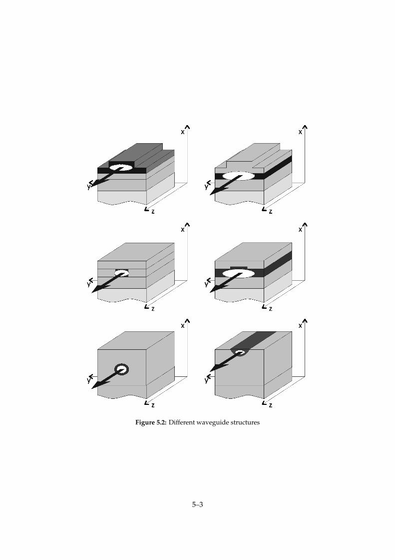
Figure 5.2: Different waveguide structures
5–3

cation, in scanners and in CD-players. The same remarks as in the InP/InGaAsP materialsystem concerning coupling to an optical fiber hold.
• Glass
Waveguides in glass are fabricated using two different types of technologies: diffusion anddeposition. The first technique is based on the ion exchange process in special types ofglasses by pure thermal or field assisted diffusion. The second technique is based on thedeposition of glass (Silica or SiO2) by means of chemical vapour deposition (CVD) or flamehydrolysis (FHD) on a substrate, mostly Silicon. The large waveguide cross-section allowseasy coupling with optical fibers. These are currently the preferred methods for fabricatingpassive optical integrated circuits. Because of the low index contrast, devices are relativelybig however.
• LiNbO3
Lithium niobate is an anisotropic crystalline material with strong electro-optical and acousto-optical properties. Waveguides are fabricated using a diffusion process. Due to the anisotropycomponents always show a large polarization dependence. The electro-optical effect is usedto realize efficient optical switches.
• Polymers
Polymers represent a broad set of materials. For purely passive applications polycarbonate(also used for compact disks) and PMMA are the preferred materials. Other types of poly-mers show a large electro-optical or non-linear coefficient but this is mostly at the expenseof a reduced long term stability.
• Silicon-on-Insulator
Waveguides are fabricated in a Silicon layer (high refractive index), which is bonded on aSilicon wafer via an intermediary silica layer (low refractive index). SOI waveguides exist intwo different varieties with very different properties: ”fiber matched” (typical dimensionsaround 7µm) and high-contrast (typical dimensions 500nm). The advantage of using Silicon-on-Insulator is that standard CMOS technology can be used to fabricate the waveguides.Even CMOS-electronics and optical circuits can be combined on the same substrate. Thehigh-contrast waveguides open the way to very large scale integrated optics.
For a long time, III-V technologies were thought to push aside other technologies because theywere the only ones allowing for monolithic integration. But due to the complicated fabricationprocess, the high cost, the high fiber to chip coupling losses and the high propagation losses of III-V waveguides, different material systems tend to co-exist, each used for their specific application.The chart below gives an overview of the most important properties of the materials discussedhere (T: Telecom / I: Interconnect).
5–4

InP GaAs Glass LiNbO3 Polymers SOITransmitters/Receivers Yes Yes No No No NoPassive optics Yes Yes Yes Yes Yes YesWavelength range T I T,I T,I T,I TFiber to chip coupling loss >2 >2 0.4 <1 <0.5 1Propagation losses (dB/cm) 2 2 <0.1 <0.3 0.1-1.5 2dn/dT [10−4/K] 1.8 2.5 <0.1 <0.1 0.1-1.5 1.7|nTE − nTM| [10−4] 0.1-10 2-10 0.1-0.5 400 2-50 0.1-...long term stability + + + + ? +wafer dimensions 2-3 inch 3 inch ≥ 4 inch 3 inch ≥ 8 inch 8-12 inch
Fiber to chip coupling losses can be improved by the use of tapers.
5.2 Modes of Optical Waveguides
5.2.1 Introduction
The starting point for the theoretical treatment of the interaction of light and dielectric structuresare Maxwells equations. We only assume isotropic and non-magnetic media and a harmonic timedependence of ejωt. In this case, and in the absence of sources and currents, we can write Maxwellsequations as (see also chapter 2):
∇× E(x, y, z) = −jωµ0H(x, y, z)∇×H(x, y, z) = jωε(x, y, z)E(x, y, z)∇ · (ε(x, y, z)E(x, y, z)) = 0∇ ·H(x, y, z) = 0
(5.1)
In these equations the constitutive relations
D = εE = ε0n2E
B = µ0H(5.2)
are implicitly assumed. The real part of the refractive index profile n(x, y, z, ω) relates the wave-length inside the medium λ = λ0
Re(n) and the vacuum wavelength λ0. The imaginary part of therefractive index describes the absorption (or gain) of the optical field.
Based on the Maxwells curl equations, vectorial wave equations for the electric field E and mag-netic field H can be written as
∇2E(r) +∇(∇n2(r)
n2(r) E(r)) + k20n
2(r)E(r) = 0
∇2H(r) + ∇n2(r)n2(r) × (∇×H(r)) + k2
0n2(r)H(r) = 0
(5.3)
In these equations the gradient of the refractive index occurs, which couples the three componentsof the field vector. When the refractive index is piecewise constant however, or if the variationof the refractive index is small, we can neglect these gradients so both vectorial equations (5.3)
5–5
decouple and reduce to the Helmholtz equation for every component of the field vector (bothelectric and magnetic field)
∇2Ψ(r) + k20n
2(r)Ψ(r) = 0 (5.4)
For the further study of optical waveguides, the boundary conditions at the interface between twoisotropic materials with dielectric constants ε1 and ε2 are important. These are:
n× (E1 − E2) = 0n× (H1 −H2) = 0n · (ε1E1 − ε2E2) = 0n · (H1 −H2) = 0
(5.5)
, which means that the tangential components of the electric and the magnetic field and the normalcomponent of the magnetic field are continuous at an interface. The normal component of theelectric field is discontinuous at an interface.
By applying these boundary conditions the field components will in general be related (althoughthey seemed to be uncoupled by neglecting the refractive index gradient terms in equation (5.3)).Note that it is often sufficient to apply the boundary conditions for the tangential componentsbecause then automatically the boundary conditions for the normal components are met.
The general solution of Maxwells equations for an arbitrary dielectric structure ε(x, y, z) requiresthe solution of a complex set of partial differential equations and requires a lot of computationpower. Therefore, in the early days of integrated optics, a lot of effort was put in the developmentof acceptable approximated calculation methods. A typical example is the effective index method.As more powerful computers became available, numerical methods like finite differences and fi-nite elements methods were used for the analysis of waveguide structures. Nevertheless, approx-imated solutions in general and the effective index method in particular remain very importantdesign and modeling tools. Some of the methods will be described later in this chapter.
5.2.2 Modes of longitudinally invariant dielectric waveguide structures
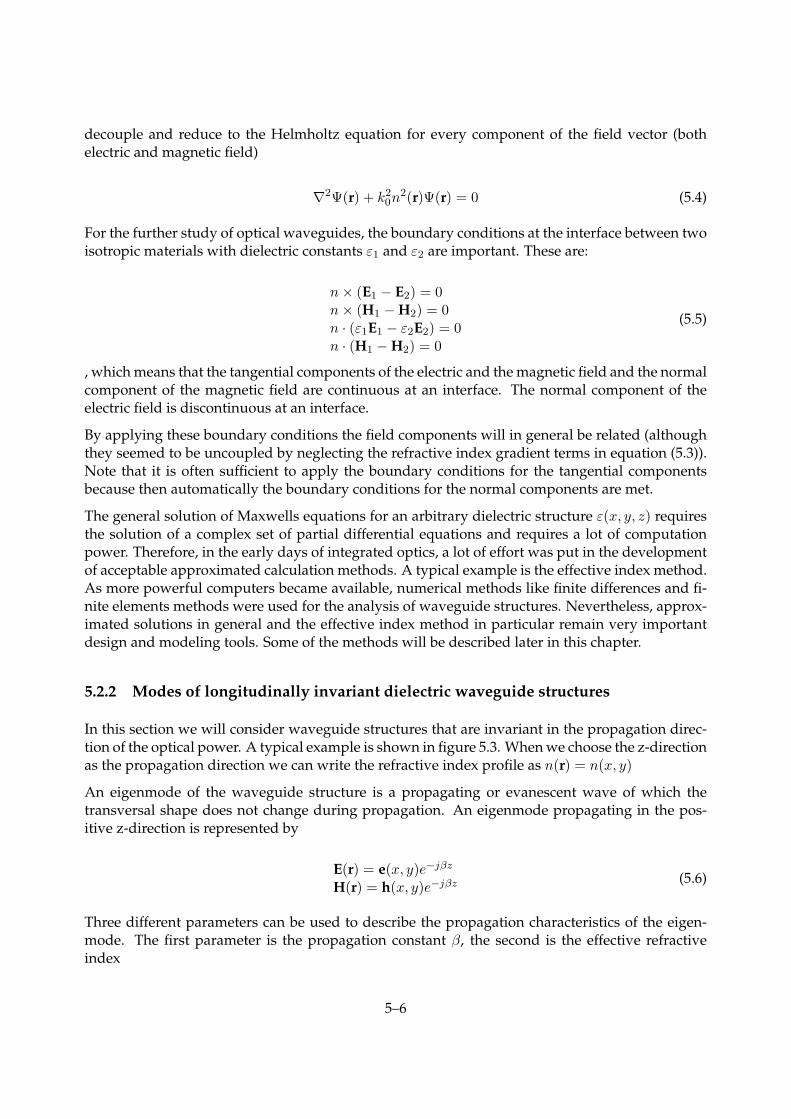
In this section we will consider waveguide structures that are invariant in the propagation direc-tion of the optical power. A typical example is shown in figure 5.3. When we choose the z-directionas the propagation direction we can write the refractive index profile as n(r) = n(x, y)
An eigenmode of the waveguide structure is a propagating or evanescent wave of which thetransversal shape does not change during propagation. An eigenmode propagating in the pos-itive z-direction is represented by
E(r) = e(x, y)e−jβz
H(r) = h(x, y)e−jβz(5.6)
Three different parameters can be used to describe the propagation characteristics of the eigen-mode. The first parameter is the propagation constant β, the second is the effective refractiveindex
5–6

Figure 5.3: Longitudinally invariant waveguide
neff =β
k0(5.7)
and the third parameter is the effective dielectric constant
εeff = n2eff (5.8)
In the following section we will show that this is the eigenvalue of the eigenvalue equation re-sulting from Maxwells equations and for which the eigenmodes are the solutions we are lookingfor. Before we continue with a detailed analysis of the eigenvalue problem, we will first list someimportant properties of lossless optical waveguides, namely waveguides for which
Im(ε(x, y)) = 0 (5.9)
Figure 5.4 shows the dielectric profile of a hypothetic waveguide together with different eigen-modes of the structure. Theoretically one can show that
1. There are no eigenmodes with an eigenvalue larger than the maximum of the dielectric func-tion.
εeff < max(ε(rt)) (5.10)
2. Guided modes belong to a discrete set of eigenvalues. These are in the range
εmax > εeff > max(εclad) (5.11)
For these modes
5–7

Figure 5.4: Eigenmodes in an optical waveguide
lim|rt|→∞
Ψ(rt) = 0 (5.12)
Note that there are waveguide structures that do not support a guided mode.
3. The continuous part of the spectrum is formed by the radiating modes for which the eigen-values
εeff < max(εclad) (5.13)
Radiating modes show an oscillating behaviour along at least one side of the waveguidestructure. Depending on their effective refractive index they are classified as propagating orevanescent radiating modes. In the last case the effective refractive index is purely imagi-nary.
4. Guided and radiating modes form a complete set of functions. This means that every fieldinside the waveguide can be represented by a sum of these modes:
E(x, y, z) =∑m
amem(x, y)e−jβmz +∫a(k)ek(x, y)e−jkzdk (5.14)
In this equation we can see the discrete sum of the guided modes and the continuous spec-trum of radiating modes.
Note that a radiating mode can be associated with a plane wave incident from the side (figure5.5).
5.2.3 The slab waveguide
A further simplification to analyze waveguide structures is to consider waveguide structures thatare not only invariant in the propagation direction but also in the direction perpendicular to the
5–8
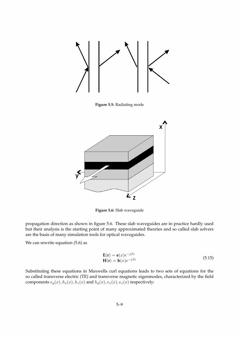
Figure 5.5: Radiating mode
Figure 5.6: Slab waveguide
propagation direction as shown in figure 5.6. These slab waveguides are in practice hardly usedbut their analysis is the starting point of many approximated theories and so called slab solversare the basis of many simulation tools for optical waveguides.
We can rewrite equation (5.6) as
E(r) = e(x)e−jβz
H(r) = h(x)e−jβz(5.15)
Substituting these equations in Maxwells curl equations leads to two sets of equations for theso called transverse electric (TE) and transverse magnetic eigenmodes, characterized by the fieldcomponents ey(x), hx(x), hz(x) and hy(x), ex(x), ez(x) respectively:
5–9

TE
βey(x) = −ωµ0hx(x)dey(x)dx = −jωµ0hz(x)
ω0ε0n2(x)ey(x) = −βhx(x) + j dhz(x)
dx
TM
βhy(x) = ωε0n
2(x)ex(x)dhy(x)dx = jωε0n
2(x)ez(x)ωµ0hy(x) = βex(x)− j dez(x)
dx
(5.16)
in which εr(x) is replaced by n2(x). By eliminating the x and z field components we can derive asecond order differential equation for ey(x) and hy(x) respectively:
d2ey(x)dx2 + k2
0n2(x)ey(x) = β2ey(x)
ddx( 1
k20n
2(x)
dhy(x)dx ) + hy(x) = β2
k20n
2(x)hy(x)
(5.17)
An important type of slab waveguide is the so called multi layer slab waveguide. This waveguideconsists of a number of layers with refractive index ni. Because the refractive index is piecewiseconstant in the multi layer slab waveguide, we can rewrite equations 5.17 as
d2ey,i(x)dx2 + k2
0n2i ey,i(x) = β2ey,i(x)
ddx( 1
k20n
2i
dhy,i(x)dx ) + hy,i(x) = β2
k20n
2ihy,i(x)
(5.18)
and the TE and TM equations become identical. Solutions will be different however because ofthe different boundary conditions for TE and TM field components at the interfaces between thedifferent layers. We will continue to work with the TE equation, in order not to overload thenotation. The analysis for the TM equation is similar.
The general solution to equation 5.18 can be written as
ey,i = Aiejkx,i(x−ai) +Bie
−jkx,i(x−ai) (5.19)
with
kx,i =√k2
0n2i − β2 (5.20)
The used notations are clarified in figure 5.7.
Based on equations 5.5 we can derive the following boundary conditions for the interface betweentwo layers:
ey,i(ai) = ey,i+1(ai)dey,i(ai)
dx = dey,i+1(ai)dx
(5.21)
apply. Using equations 5.21 and 5.19 we can derive the following matrix relation:
5–10

Figure 5.7: Multi layer slab waveguides
[AiBi
]=
12αi
[(αi + αi+1)e−δi+1 (αi − αi+1)eδi+1
(αi − αi+1)e−δi+1 (αi + αi+1)eδi+1
] [Ai+1
Bi+1
](5.22)
By repeating this procedure for all layers, the following matrix equation can be derived:
[A1
B1
]=[t11(β2) t12(β2)t21(β2) t22(β2)
] [ANBN
](5.23)
For guided modes
limx→±∞
ey(x) = 0 (5.24)
and because β > k0nN and β > k0n1 we can write that A1 = BN = 0 (if we choose +j as thesolution to
√−1). From equation 5.23 we can see that this can only be fulfilled if t11(β2) = 0. The
solutions to this dispersion equation yield the guided modes of the structure. Note that this matrixdescription actually is identical to the analysis for the reflection and transmission of a plane waveat a layer stack discussed in the previous chapter.
Finding the solutions to the dispersion equation has to be done numerically. Only in the case of a3-layer slab waveguide some interesting properties can be derived analytically.
In the case of a 3-layer slab waveguide, equation 5.19 can be written as (with the notations asdepicted in figure 5.2.3)
ey = Ae−δx (x ≥ 0)ey = A cos(κx) +B sin(κx) (− d ≤ x ≤ 0)ey = (A cos(κd)−B sin(κd))eγ(x+d) (x ≤ −d)
(5.25)
With
5–11
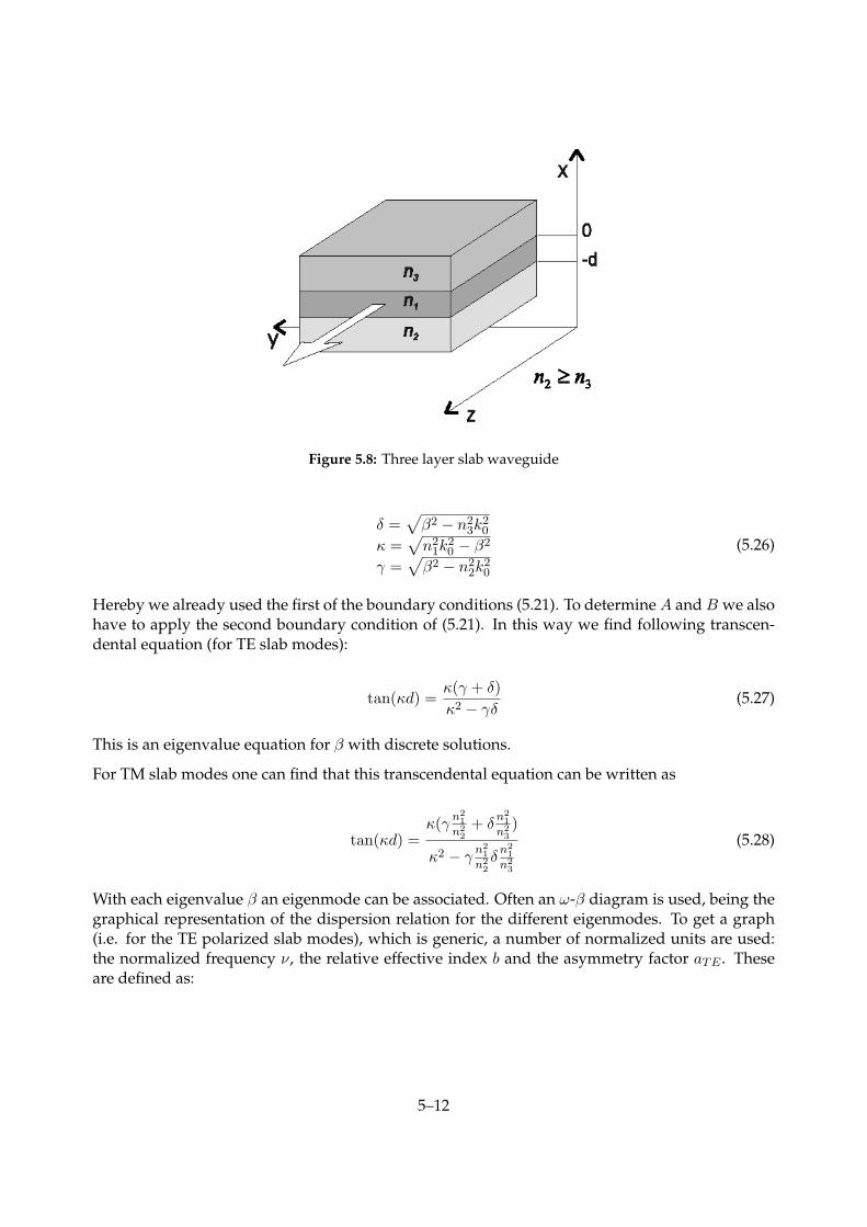
Figure 5.8: Three layer slab waveguide
δ =√β2 − n2
3k20
κ =√n2
1k20 − β2
γ =√β2 − n2
2k20
(5.26)
Hereby we already used the first of the boundary conditions (5.21). To determine A andB we alsohave to apply the second boundary condition of (5.21). In this way we find following transcen-dental equation (for TE slab modes):
tan(κd) =κ(γ + δ)κ2 − γδ
(5.27)
This is an eigenvalue equation for β with discrete solutions.
For TM slab modes one can find that this transcendental equation can be written as
tan(κd) =κ(γ n
21
n22
+ δn2
1
n23)
κ2 − γ n21
n22δn2
1
n23
(5.28)
With each eigenvalue β an eigenmode can be associated. Often an ω-β diagram is used, being thegraphical representation of the dispersion relation for the different eigenmodes. To get a graph(i.e. for the TE polarized slab modes), which is generic, a number of normalized units are used:the normalized frequency ν, the relative effective index b and the asymmetry factor aTE . Theseare defined as:
5–12

Figure 5.9: Waveguide dispersion curves
ν = k0d√n2
1 − n22
b =n2eff−n
22
n21−n2
2
aTE = n22−n2
3
n21−n2
2
(5.29)
These definitions result in the dispersion curves depicted in figure 5.9 for TE eigenmodes (fordifferent values of the asymmetry factor aTE .
The number of guided TE modes can be calculated from equation 5.50 to 5.27:
M = 1 + Int[1π
(ν −Arctan(√aTE)] (5.30)
In this equation Int[. . . ] means the integer part of the argument. For symmetrical waveguides thisformula is simplified to M = 1 + Int[ νπ ]. So there is at least 1 guided mode. In the case of a sym-metrical waveguide knowing the normalized frequency ν is sufficient to determine the amount ofguided modes. Therefore this number is frequently used when describing optical waveguides.
Note that the effective index can be considered as some kind of average refractive index felt bythe guided mode. In this context we can also define the confinement factor Γ. It is defined (for TEpolarization) as
ΓTEi =
∫iE
2ydx∫ +∞
−∞ E2ydx
(5.31)
and is a measure for the confinement of the eigenmode inside layer i. Obviously
5–13
N∑i=1
ΓTEi = 1 (5.32)
The confinement factor is often used in the theory of laser operation, to denote which part of theoptical power is located inside the active layer, where there is gain.
5.2.4 The effective index method
Lets return to the two-dimensional waveguide. For many waveguide types the lateral dimensionsare larger than the transversal dimensions. Moreover, the vertical index contrast often is very low.In that case, the modes of the waveguide often will show a quasi-TE or quasi-TM behaviour andcan be approximately described by the scalar Helmholtz equation. The effective index methodgives an approximate solution to this equation.
As said, the starting point for the effective index method is the scalar Helmholtz equation:
∇2Ψ(x, y, z) + k20n
2(x, y)Ψ(x, y, z) = 0 (5.33)
In this equation Ψ can be replaced by any of the field components. Because we are still consideringlongitudinally invariant waveguide structures, the z dependence of Ψ(x, y, z) is given by
Ψ(x, y, z) = ψ(x, y)e−jβz (5.34)
This way, equation (5.33) becomes
∇2xyψ(x, y) + (k2
0n2(x, y)− β2)ψ(x, y) = 0 (5.35)
This equation can be solved in a number of ways. A first method is the effective index methodwhich is an approximate solution. We start from the assumption that we can write
ψ(x, y) = F (x, y)G(y) (5.36)
in which F (x, y) is a slowly varying function of y, so that we can write that
∂F
∂y= 0 (5.37)
Substitution of equation 5.36 in equation 5.35 leads to
F (x, y)d2G(y)dy2
+ 2∂F (x, y)∂y
dG(y)dy
+G(y)[∂2F (x, y)∂x2
+∂2F (x, y)∂y2
]+ (n2k2
0 − β2)F (x, y)G(y) = 0
(5.38)
5–14

Figure 5.10: Effective index method
Using equation 5.37 this becomes
1G
d2G
dy2+
1F
∂2F
∂x2+ (k2
0n2(x, y)− β2) = 0 (5.39)
We now apply a technique closely resembling the classical technique of separation of variables.The only difference is that F (x, y) shows a weak dependence on y and that we have to introducean y-dependent separation variable neff (y). This way we find
1F∂2F∂x2 + k2
0n2(x, y) = k2
0n2eff (y)
1Gd2Gdy2 − β2 = −k2
0n2eff (y)
(5.40)
These are the fundamental equations of the effective index method. Lets consider the first equa-tion. We divide the two dimensional waveguide in slices for which we can assume the refractiveindex profile as being independent of y. This is very easy for piecewise constant refractive in-dex profiles but is also possible for a continuously varying index profile by applying a staircaseapproximation (figure 5.10).
Equation (5.40) then reduces to
∂2Fi∂x2
+ k20n
2i (x)Fi = k2
0n2eff,iFi (5.41)
If we compare this equation with equation (5.17a) then it is clear that neff,i is the effective indexof a one dimensional slab waveguide with a refractive index profile ni(x). The correspondingmode profile determines Fi(x). Solving the first equation of (5.40) leads to an effective indexdistribution neff (y). Using this function we can solve the second equation of (5.40). This equationcan be rewritten as
5–15

Figure 5.11: one dimensional equivalent
d2G
dy2+ (k2
0n2eff (y)− β2)G = 0 (5.42)
Again, this is the equation for a one dimensional slab waveguide with refractive index profileneff (y). Solving this equation results in the propagation constant β and the mode profile G(y).
Although this method is in principle a scalar method, it still allows to take the polarization of themode ψ(x, y) into account. Say we are interested in the TE eigenmode of the two dimensionalwaveguide. The electric field vector of the mode is pointing along the y-axis, just like for the TEslab modes Fi(x). To keep the same polarization state for the second equation this equation has tobe solved for TM polarization. To calculate the TM eigenmode of the two dimensional waveguide,the appropriate boundary conditions need to be applied.
The errors made using the effective index method are due to the fact that equation (5.37) doesnot apply. This is the case in the vicinity of vertical dielectric interfaces. Generally speaking theeffective index method will overestimate the propagation constants of the waveguide modes.
The effective index method is not only used to calculate two dimensional mode profiles and its cor-responding propagation constants. More often it is used to simplify a two dimensional transversalwaveguide structure to a one dimensional structure which can serve as a starting point for furtheranalysis methods like the mode expansion method or the beam propagation method (figure 5.11).
5.2.5 Numerical methods
Numerical methods like finite difference or finite element methods start of from the vectorial equa-tions or the scalar Helmholtz equation. In a finite difference method, the first step always is thediscretization of the refractive index profile. To do this the waveguide is put inside a box withdimensions that are sufficiently large to suppose that the fields are zero on the edges of the box.Next, the box is divided into basic cells in which the refractive index is constant (meshing). De-pending on the meshing algorithm, the mesh will or will not be equidistant.
In a second step the field equations are discretized by replacing the derivatives by their finitedifference representation. In this way the set of partial differential equations is replaced by alinear set of equations which can be solved using standard algebraic methods.
The errors due to the finite difference method have two causes. There is the finite differenceapproximation of the derivatives and on the other side the approximation that the fields are zero
5–16

Figure 5.12: Discretization for numerical methods
on the edges of the box. To reduce these errors the discretization of the mesh can be refined andthe dimensions of the box can be increased.
Note that there is a fundamental difference between the errors due to an approximate methodlike the effective index method and a numerical method like the finite difference method. Withnumerical methods we can start of with the exact Maxwell equations and the error can alwaysbe reduced by refining the discretization parameter, at the expense of larger calculation times. Inapproximated methods like the effective index methods, the equations are solved rigorously, butthe equations are only approximations of Maxwells equations.
5.2.6 Modes of metal-dielectric surface plasmon waveguide structures
In this section we will discuss the waveguiding properties of an interface between a semi-infinitemetal with a complex permittivity εm = ε′m + jε′′m and a semi-infinite dielectric with permittivityεd = ε′d + jε′′d, as shown in figure 5.2.6.
While this layer structure consists only of two semi-infinite materials, one can still look for guidedmodes with a propagation constant β. If these guided modes exist, their propagation constants canbe found by solving the eigenvalue equation 5.27 and 5.28 for TE and TM polarization respectively,by letting d approach to zero, as this two-layer waveguide can be treated as a limiting case of thethree-layer waveguide stack discussed in the previous section. For TE polarization, this results inan eigenvalue equation
γ = −δ (5.43)
while for TM polarization the eigenvalue equation becomes
γ
εm+
δ
εd= 0 (5.44)
with
5–17

Figure 5.13: Example of 2D mode calculation using a numerical method. The upper row of plots showsthe 0th and 1st order TE mode of a rib waveguide. The second row of plots shows the symmetric andantisymmetric TE mode in two coupled waveguides of the same type as the first row.
Figure 5.14: In this graph we show the effective index of the 0th order mode (TE and TM) of the depicted ribwaveguide, calculated using a numerical mode solver (exact) and the effective index method. The guidinglayer of the rib waveguide is 0.6µm thick. In the low index contrast case (not etched in the guided layer (t <0)) the results of the effective index method closely resemble the exact results. Also when the waveguide isetched completely through the guiding layer (t > 0.6µm) this is the case. Only in the intermediate area theapproximation is less good.
5–18
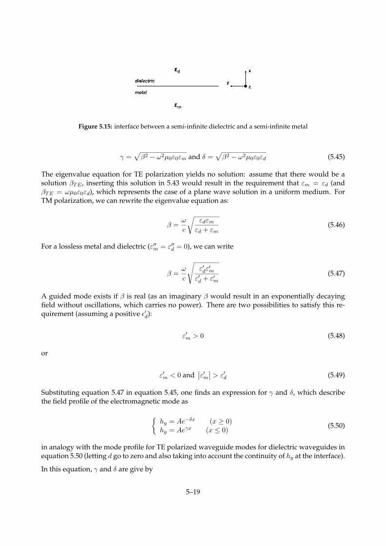
Figure 5.15: interface between a semi-infinite dielectric and a semi-infinite metal
γ =√β2 − ω2µ0ε0εm and δ =
√β2 − ω2µ0ε0εd (5.45)
The eigenvalue equation for TE polarization yields no solution: assume that there would be asolution βTE , inserting this solution in 5.43 would result in the requirement that εm = εd (andβTE = ωµ0ε0εd), which represents the case of a plane wave solution in a uniform medium. ForTM polarization, we can rewrite the eigenvalue equation as:
β =ω
c
√εdεmεd + εm
(5.46)
For a lossless metal and dielectric (ε′′m = ε′′d = 0), we can write
β =ω
c
√ε′dε′m
ε′d + ε′m(5.47)
A guided mode exists if β is real (as an imaginary β would result in an exponentially decayingfield without oscillations, which carries no power). There are two possibilities to satisfy this re-quirement (assuming a positive ε′d):
ε′m > 0 (5.48)
or
ε′m < 0 and∣∣ε′m∣∣ > ε′d (5.49)
Substituting equation 5.47 in equation 5.45, one finds an expression for γ and δ, which describethe field profile of the electromagnetic mode as
hy = Ae−δx (x ≥ 0)hy = Aeγx (x ≤ 0)
(5.50)
in analogy with the mode profile for TE polarized waveguide modes for dielectric waveguides inequation 5.50 (letting d go to zero and also taking into account the continuity of hy at the interface).
In this equation, γ and δ are give by
5–19

Figure 5.16: hy-field of a surface plasmon propagating at the interface between a semi-infinite dielectricand a semi-infinite metal
γ =ω
c
√−ε′2m
ε′m + ε′d(5.51)
and
δ =ω
c
√−ε′2d
ε′m + ε′d(5.52)
When ε′m < 0 and |ε′m| > ε′d (condition 5.49), both γ and δ are real and positive, implying thatthe hy field component of the mode guided at the metal-dielectric interface consists of two ex-ponentially decaying functions, as shown in figure 5.2.6. This mode, which exists at the interfacebetween a semi-infinite dielectric and (perfect) metal is referred to as a surface plasmon mode. Theex and ez field components can easily be calculated from equation 5.16. These are also exponen-tially decaying (with ez being continuous at the interface, while there is a discontinuity in the excomponent). The fields typically penetrate much deeper into the dielectric than into the metal. Thefact that the field peaks at the interface, makes the propagation properties of the surface plasmonmode very sensitive to possible variations in the refractive index at the metal-dielectric interfaceand these modes can therefore be used to sense the presence of a very thin layer at the metalsurface (e.g. the detection of a monolayer of proteins at a chemically activated gold surface).
When ε′m > 0, γ and δ will be imaginary, meaning that the light will not be bound to the interface,and radiate into the two semi-infinite media (radiative surface plasmon mode).
While we assumed a perfect metal in the above discussion, the theory can be extended for the caseof a lossy metal. The above conclusions remain valid, while the propagation constant obtains animaginary part which describes the loss the surface plasmon mode experiences when travellingalong the metal-dielectric interface. Propagation lengths are typically in the order of 10 to 100µm,depending on the metal used and the wavelength.
The real part of the dielectric function of a metal can be described by (according to the free electronmodel of Drude)
ε′1(ω) = 1−ω2p
ω2(5.53)
5–20

with ωp the plasma-frequency. Therefore, a non-radiating surface plasmon (ε′m < 0 and |ε′m| > ε′d)can only exist when
ω <ωp√
1 + ε′d(5.54)
while radiating surface plasmons (ε′m > 0) occur when ω > ωp.
5.3 Propagation through dielectric waveguide structures
In this section we will discuss the propagation of light through waveguide structures for which thetransversal cross section varies along the propagation direction. In some cases approximated semi-analytical calculation methods can be used (mode expansion, coupled mode theory, supermodetheory). In most cases a complete numerical treatment will be necessary.
5.3.1 Mode expansion and propagation method
We assume a one dimensional z invariant waveguide that is excited by a field distribution Ψ(x, z)and we want to see how this field looks like after propagating through the waveguide over adistance L.
The eigenmodes of the waveguide form a complete set and are orthonormal, so we can write
Ψ(x, z = 0) =N−1∑i=0
aiψi(x) with
+∞∫−∞
ψi(x)ψj(x)dx = δij (5.55)
In this equation ψi is the i-th eigenmode of the waveguide. This sum includes all eigenmodes(both the guided and radiating eigenmodes, for which the sum actually has to be replaced by anintegral). The expansion coefficients ai can easily be calculated. By multiplying equation (5.55)with ψj and integrating this equation from −∞ to +∞we find
aj =
+∞∫−∞
Ψ(x, z = 0)ψj(x)dx (5.56)
The propagation of the individual eigenmodes through the waveguide is trivial (multiplyingeach eigenmode by its propagation factor e−jβjz). The field Ψ(x, z)after propagation through thewaveguide over a distance L is then given by
Ψ(x, z = L) =N−1∑i=0
+∞∫−∞
Ψ(x, z = 0)ψi(x)dx
ψi(x)e−jβiL (5.57)
5–21
Suppose this waveguide is coupled to another, also z-invariant waveguide, with eigenmodesφi(x). If we assume that there are no reflections (which is an approximation), the output fieldof the first waveguide becomes the input field of the second waveguide. Just like in equation(5.55) we can decompose this field in the eigenmodes of the second waveguide
Ψ(x, z = L) =N−1∑i=0
aiψi(x)e−jβiL =M−1∑j=0
bjφj(x) (5.58)
Because also the eigenfunctions φi(x) are orthonormal, we can find an expression for bk:
bk =
+∞∫−∞
Ψ(x, z = L)φk(x)dx =N−1∑i=0
ai
+∞∫−∞
ψi(x)φk(x)dxe−jβiL (5.59)
We can now propagate the field (5.58) through the second waveguide:
Ψ(x, z = L+ L′) =M−1∑j=0
bjφje−jγjL′ (5.60)
in which γj are the propagation constants of the eigenmodes in the second waveguide. This pro-cedure can be repeated as often as required and can be written down easily in a matrix notation.
Note that at every vertical waveguide discontinuity a reflected field originates. So, not only thecoupling of the eigenmodes of the first waveguide to the eigenmodes of the second waveguideneeds to be taken into account, but also the coupling back to the eigenmodes of the first waveg-uide needs to be considered. When there is only a weak discontinuity these reflections can oftenbe neglected and in such a case the unidirectional mode expansion propagation method describedabove applies. In some cases it is necessary however to include the reflections and then a bidirec-tional eigenmode expansion propagation method has to be used.
Figure 5.17a shows how the propagation of a field through a gradually broadening waveguidecan be calculated by means of the mode expansion method. Here, the discontinuities are smalland we can neglect the reflected field. For the codirectional coupler of figure 5.17b this is not thecase. In this case reflections play an important role and a bidirectional method has to be used.
5.3.2 Coupled mode theory
In a regular z-independent waveguide, eigenmodes are orthonormal and propagate in an inde-pendent way. The complete field can be written as a linear combination of the eigenmodes. Insome situations the waveguide structure can be seen as a small perturbation of the simple z-independent waveguide structure. In that case, the field can still be written in terms of the modesof the simple waveguide structure, but due to the perturbation these modes will no longer bedecoupled. In the case two modes are dominant, the field can be written as:
Ψ(x, z) = C1(z)e−jβ1zψ1(x) + C2(z)e−jβ2zψ2(x) (5.61)
5–22

Figure 5.17: Waveguide structures
Figure 5.18: Coupled mode theory
Fast longitudinal variations are taken into account by the propagation factor e−jβiz while the z-dependent coefficients C1(z) and C2(z) describe the coupling between the two modes ψ1 and ψ2.An alternative formulation takes all longitudinal variations together in one term Xi(z):
Ψ(x, z) = X1(z)ψ1(x) +X2(z)ψ2(x) (5.62)
We will continue to use the formulation used in equation (5.62). Depending on the envisionedstructure an appropriate choice of ψ1 and ψ2 has to be made. In figure 5.18 a typical exampleis shown of a waveguide structure where coupled mode theory can be applied. Is this case wechoose ψ1 and ψ2 to be the waveguide modes of the unperturbed waveguides. Note that we canconsider this system to be double perturbed.
The uncoupled modes ψ1 and ψ2 satisfy following propagation equations:
5–23

dX1dz = −jβ1X1dX2dz = −jβ2X2
(5.63)
with the obvious solution
X1(z) = e−jβ1z
X2(z) = e−jβ2z (5.64)
Coupled mode theory postulates that linear coupling terms need to be added to this equation todescribe the perturbed system
dX1(z)dz = −jβ1X1(z)− j(κ11X1 + κ12X2)
dX2(z)dz = −jβ2X2(z)− j(κ21X1 + κ22X2)
(5.65)
We will assume that the coupling coefficients are z-independent and that both modes travel inthe same direction (uniform codirectional coupling). Normally, some other assumptions are alsomade:
• The two modes are normalized
• The total power flux in the system can be calculated by the sum of the power carried byevery mode seperately:
P (z) = |X1|2 + |X2|2 (5.66)
Modes have to be power independent for this.
• The complete system is lossless (dP (z)dz = 0). If we calculate dP (z)
dz by means of equation (5.66)and (5.65) we find that
β1, β2, κ11, κ22 are realκ21 = κ12∗
(5.67)
• Based on reciprocity and symmetry around a plane parallel to z=0 we also find (both forlossless and lossy systems) that
κ21 = κ12 (5.68)
This means that in the lossless case all coupling constants are real.
If we choose initial conditions to be X1 = 1 and X2 = 0, which means that only one of the modesis excited, integrating equation (5.65) leads to
X1(z) = e−jβz[cos(δz)− i∆
δ sin(δz)]
X2(z) = e−jβz[−iκ21
δ sin(δz)] (5.69)
5–24
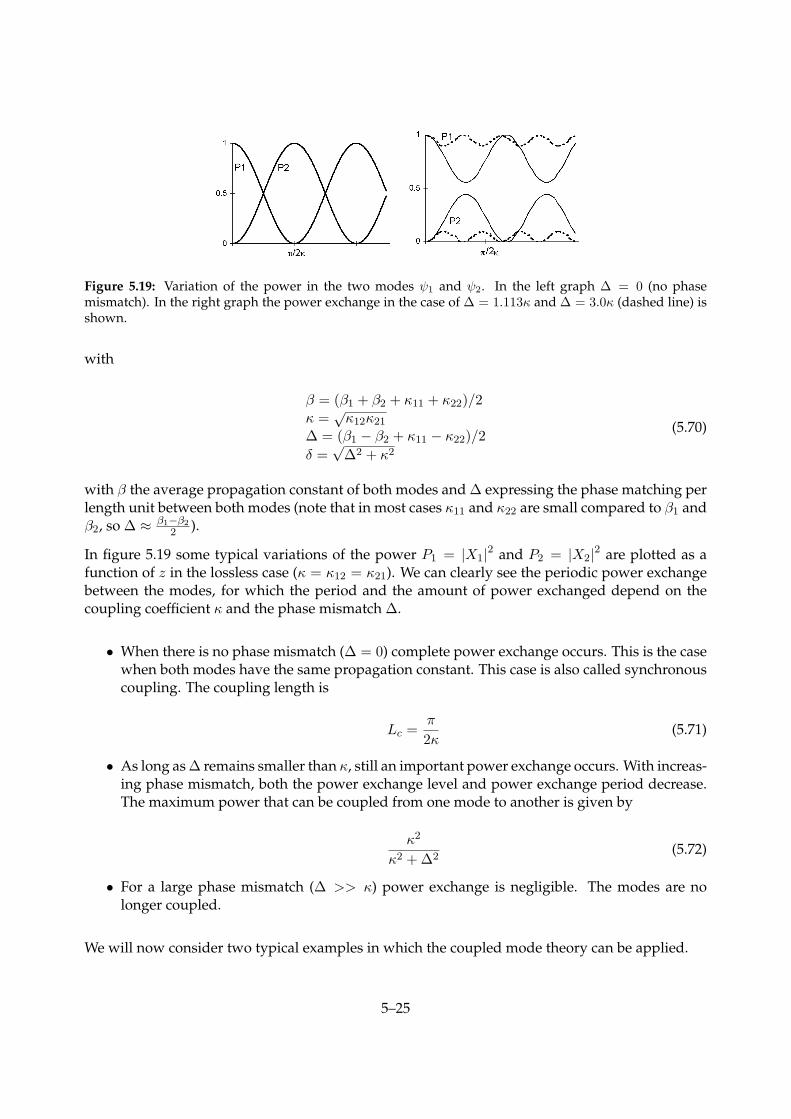
Figure 5.19: Variation of the power in the two modes ψ1 and ψ2. In the left graph ∆ = 0 (no phasemismatch). In the right graph the power exchange in the case of ∆ = 1.113κ and ∆ = 3.0κ (dashed line) isshown.
with
β = (β1 + β2 + κ11 + κ22)/2κ =√κ12κ21
∆ = (β1 − β2 + κ11 − κ22)/2δ =√
∆2 + κ2
(5.70)
with β the average propagation constant of both modes and ∆ expressing the phase matching perlength unit between both modes (note that in most cases κ11 and κ22 are small compared to β1 andβ2, so ∆ ≈ β1−β2
2 ).
In figure 5.19 some typical variations of the power P1 = |X1|2 and P2 = |X2|2 are plotted as afunction of z in the lossless case (κ = κ12 = κ21). We can clearly see the periodic power exchangebetween the modes, for which the period and the amount of power exchanged depend on thecoupling coefficient κ and the phase mismatch ∆.
• When there is no phase mismatch (∆ = 0) complete power exchange occurs. This is the casewhen both modes have the same propagation constant. This case is also called synchronouscoupling. The coupling length is
Lc =π
2κ(5.71)
• As long as ∆ remains smaller than κ, still an important power exchange occurs. With increas-ing phase mismatch, both the power exchange level and power exchange period decrease.The maximum power that can be coupled from one mode to another is given by
κ2
κ2 + ∆2(5.72)
• For a large phase mismatch (∆ >> κ) power exchange is negligible. The modes are nolonger coupled.
We will now consider two typical examples in which the coupled mode theory can be applied.
5–25

Figure 5.20: Directional coupler structure
Figure 5.21: Contradirectional grating coupler
• Directional coupler
In the case of a directional coupler, consisting of two waveguides running parallel to eachother, the coupling coefficients can easily be calculated using perturbation theory (see Ap-pendix). We find that
κ12 = k202
∫(n2
12 − n12)ψ1ψ2dx
κ21 = k202
∫(n2
12 − n22)ψ1ψ2dx
(5.73)
• Contradirectional grating coupler
In the case of a contradirectional grating coupler one chooses the modes ψ1 and ψ2 to beidentical but propagating in the opposite direction. The theory described above can then berepeated, however we have to change equation (5.66) for the z-dependent power flux to
P (z) = |X1|2 − |X2|2 (5.74)
In the chapter on periodic structures this theory will be elaborated. Applications of thecontradirectional coupler are DBR and DFB lasers.
5.3.3 Supermodes
An alternative calculation method uses the theory of supermodes 1. Lets consider again a direc-tional coupler consisting of two identical monomodal waveguides, both with fundamental mode
1Actually this is a simplified form of the general mode expansion theory described in 5.3.1
5–26

ψ0. We can also look at the structure as a whole as being a single waveguide. In this waveguidestructure a symmetrical and antisymmetrical mode φ+ and φ− with propagation constants β+ andβ− can propagate (see also figure 5.13).
When we excite one of the waveguides with its modal field ψ0 then we can write
Ψ(x, z = 0) = ψ0(x) ≈ c+φ+ + c−φ− (5.75)
with c+ = c− = 1/2. After propagation over a distance L this becomes
Ψ(x, z = L) = c+φ+e−jβ+L + c−φ−e
−jβ−L (5.76)
or
Ψ(x, z = L) = c+e−jβ+L
[φ+ + φ−e
+j(β+−β−)L]
(5.77)
When e+j(β+−β−)L = −1 all power will be concentrated in the second waveguide. This way wefind the following relation between the coupling coefficient κ and the difference β+ − β−:
β+ − β− = 2κ (5.78)
Lets now consider an asymmetrical directional coupler. The modes will no longer be perfectlysymmetrical and asymmetrical but tend to look like the modes of the individual waveguides.Equation (5.75) is still valid, but c+ will no longer equal c−.
After propagation over a distance L, we find
Ψ(x, z = L) = c+e−jβ+L
[φ+ +
c−c+φ−e
+j(β+−β−)L
](5.79)
The period of power exchange still is given by
Lc =π
β+ − β−(5.80)
but the power exchange is no longer complete. The amount of power exchange is given by c−c+
. Sowe can write
(β+ − β−) = 2δ = 2√
∆2 + κ2 (5.81)
and if |∆| >> κ
(β+ − β−) ≈ 2 |∆| ≈ |β1 − β2| (5.82)
In certain cases it occurs that the dispersion curves β1(ω) and β2(ω) of the uncoupled waveguidesintersect at a certain frequency. This means that the directional coupler operates in phase matched
5–27

Figure 5.22: Dispersion curves of uncoupled modes and super modes
conditions for this frequency (so there is strong coupling) and for other frequencies the couplingis weak (asynchronous coupling). So we get the picture as shown in figure 5.22 in which β1, β2, β+
and β− are shown as a function of frequency. From this picture it is clear that at low frequencythe supermodes resemble the propagation constant (and field profile) of one of the unperturbedmodes. At the phase matching frequency this behaviour is broken and β+−β− = 2κ. At higher fre-quencies this behaviour changes and each of the supermodes will resemble the other unperturbedwaveguide mode.
5.3.4 Beam propagation method
1. Introduction
The methods described in the previous sections only are applicable for a number of simplewaveguide structures. In most cases there will be some coupling between guided and ra-diating modes. Because of this coupling, part of the optical power will be lost. The mostimportant technique that takes into account this radiation loss is the beam propagationmethod (BPM). BPM allows to calculate the propagation of the optical field over a largedistance (compared to the wavelength) and this for very complex structures. The requiredcomputer code is fairly simple and can easily be extended to waveguides with gain and loss,to waveguides with discrete longitudinal reflections or for polarization sensitive waveguideconfigurations like in the anisotropic LiNbO3 crystal.
The BPM-method can be used to model three dimensional waveguide structures. The sim-ulation can be done in two ways. One can use a full three dimensional version of the BPMcode. This leads to the most accurate results but is very time consuming. A less time con-suming method is the combination of the effective index method and a two dimensionalBPM. This eliminates the large index contrast with air and reduces the simulation time sub-stantially. It is only useful however if the radiation towards the upper and lower half space
5–28

is negligible. In real structures this is often the case. Therefore, we will restrict ourself to thetwo dimensional BPM method. First we will discuss the classical FFT-BPM method.
2. FFT-BPM
Starting point of the discussion is the Helmholtz scalar wave equation in two dimensions
∇2Ψ(x, z) + k20n
2(x, z)Ψ(x, z) = 0 (5.83)
The square of the refractive index profile can be written as
n2(x, z) = n20 + ∆n2(x, z) (5.84)
in which n0 is a well chosen constant refractive index such that
∆n << n0 (5.85)
We propose a solution to equation (5.83) of the form:
Ψ(x, z) = ψ(x, z)e−jk0n0z (5.86)
The fast z-variations in Ψ(x, z) are covered by the propagation factor e−jk0n0z . We can as-sume that ψ(x, z) will only be weakly z-dependent, such that∣∣∣∣∂2ψ
∂z2
∣∣∣∣ << ∣∣∣∣2k0n0∂ψ
∂z
∣∣∣∣ (5.87)
This means that the amplitude function ψ(x, z) varies slowly on the scale of the materialwavelength 2π
k0n0(the so called paraxial approximation).
Substituting equation (5.86) into equation (5.83) we find that (taking equation (5.87) intoaccount)
∂ψ(x, z)∂z
= − j
2k0n0
(∂2ψ(x, z)∂x2
+ k20∆n2(x, z)ψ(x, z)
)(5.88)
This is the scalar Fresnel equation or parabolic wave equation. We can write down equation(5.88) like
∂ψ(x, z)∂z
= (T + N)ψ(x, z) (5.89)
in which
T = − j2k0n0
∂2
∂x2
N = −jk0
2n0∆n2
(5.90)
Integration of equation (5.88) can formally be determined to be
5–29

ψ(x, z + ∆z) = e(T+N)∆zψ(x, z) = eT∆z[eN∆zψ(x, z)
](5.91)
In this solution the step ∆z has to be chosen sufficiently small. On the one hand because then∆n(x, z) can be assumed z-independent over this step, on the other hand because stating that
e(T+N)∆zψ(x, z) = eT∆z[eN∆zψ(x, z)
](5.92)
which means that we apply the operators T and N sequentially and not together, is onlyvalid for sufficiently small ∆z.
This way the field is propagated stepwise through the complete waveguide structure. Wewill now study the operator e(T+N)∆z . Calculating the term
[eN∆zψ(x, z)
]is straightfor-
ward. The field ψ(x, z) is multiplied by an x-dependent phase term. The meaning of theoperator eT∆z is less obvious. Therefore we will first study the influence of the operator ona plane wave ψ = e−jkxx. Developing the operator in a Taylor expansion, we can write:
eT∆ze−jkxx = e− j∆z
2k0n0
∂2
∂x2 e−jkxx
=(
1 + (− j∆z2k0n0
∂2
∂x2 ) + 12(− j∆z
2k0n0
∂2
∂x2 )2 + ...)e−jkxx
= (1 + j2k0n0
∆zk2x + 1
2
(j
2k0n0∆zk2
x
)2+ ...)e−jkxx
= ej
2k0n0∆zk2
xe−jkxx
(5.93)
Therefore the influence of the operator on a plane wave can easily be calculated. Therefore,to calculate the influence of the operator on an arbitrary field ψ(x, z) we first take the fouriertransform of the field. On this plane wave expansion we can apply the operator eT∆z . Bydoing an inverse fourier transform we find the result of eT∆zψ(x, z). Note that this is equiv-alent to the propagation of an arbitrary field through a homogenous medium with refractiveindex n0.
The calculation of the propagated field ψ(x, z = ∆z) out of the original field ψ(x, z) is doneas follows. First a phase correction, due to the index perturbation, is applied (operator eN∆z).Then the field is decomposed into its plane wave components, these are individually propa-gated through a homogenous medium with refractive index n0 and then recomposed to thecomplete field distribution (operator eT∆z).
Note: Calculating e(T+N)∆zψ(x, z) as eT∆z[eN∆zψ(x, z)
]is only an approximation. This is
because the operators do not commute. A better approximation is to write
e(T+N)∆zψ(x, z) = e( T2
)∆zeN∆ze( T2
)∆zψ(x, z) +O(T 3, N3) (5.94)
The analysis is completely analogous to the previous one.
3. Expanding the theory
FFT-BPM method is not often used any more. In most commercial modeling tools a finitedifference BPM algorithm is used. In a finite difference BPM the paraxial wave equationis directly discretized, both longitudinally and transversally. Other extensions to the BPMalgorithm are related to
5–30

• the waveguide structure which is not paraxial (i.e. equation (5.87) is no longer valid)• vectorial calculations• reflections• 3D waveguides• numerical accuracy and efficiency• high contrast waveguides• improved boundary conditions
5.4 Optical components
5.4.1 Loss in straight waveguides
In the previous section the straight waveguide was already extensively analyzed. In this sectionwe will therefore restrict ourself to an aspect that has not yet been dealt with: propagation lossesin waveguides. There are different causes for this loss. The interaction of light and matter resultin absorption and non perfect guiding results in scattering and radiation losses.
When the origin of the loss is uniformly spread over the waveguide length, the guided opticalpower will decrease exponentially with the propagation distance.
P (z) = P0e−αz (5.95)
α is called the power attenuation coefficient. Due to the typical dimensions of an integrated opticalcircuit (cm scale) α typically has to be below 0.1 to 1.0 cm−1, which corresponds to a loss between0.5dB/cm to 5dB/cm. We will now discuss the different loss mechanisms which cause these losses.
• Loss through absorption
In semiconductor materials with a direct bandgap, the easiest absorption mechanism is theelectron-hole pair creation by a photon with a photon energy larger than the bandgap Eg.Sometimes this is wanted (photodetectors) and if this is not the case it can easily be pre-vented by choosing a material composition with a bandgap sufficiently large compared tothe photon energy.
Also free carriers play a role in the absorption process due to inter and intraband transi-tions. For non-intentionally doped semiconductors with a carrier concentration of about1016cm−3 this absorption typically remains below 0.1dB/cm. Also in non semiconductormaterial losses occur due to electronic and molecular transitions.
• Loss through scattering
Scattering losses are caused by spatial fluctuations of the refractive index (volume scattering)or by the roughness at the sidewalls of the waveguide (surface roughness scattering). Thesecan be both etched waveguide boundaries that determine the waveguide or the interface oftwo layers which are grown on top of each other. In practice mostly surface roughness scat-tering seems to be a problem. Based on some simple assumptions, following approximatedequation for the scattering loss at boundaries can be obtained
5–31
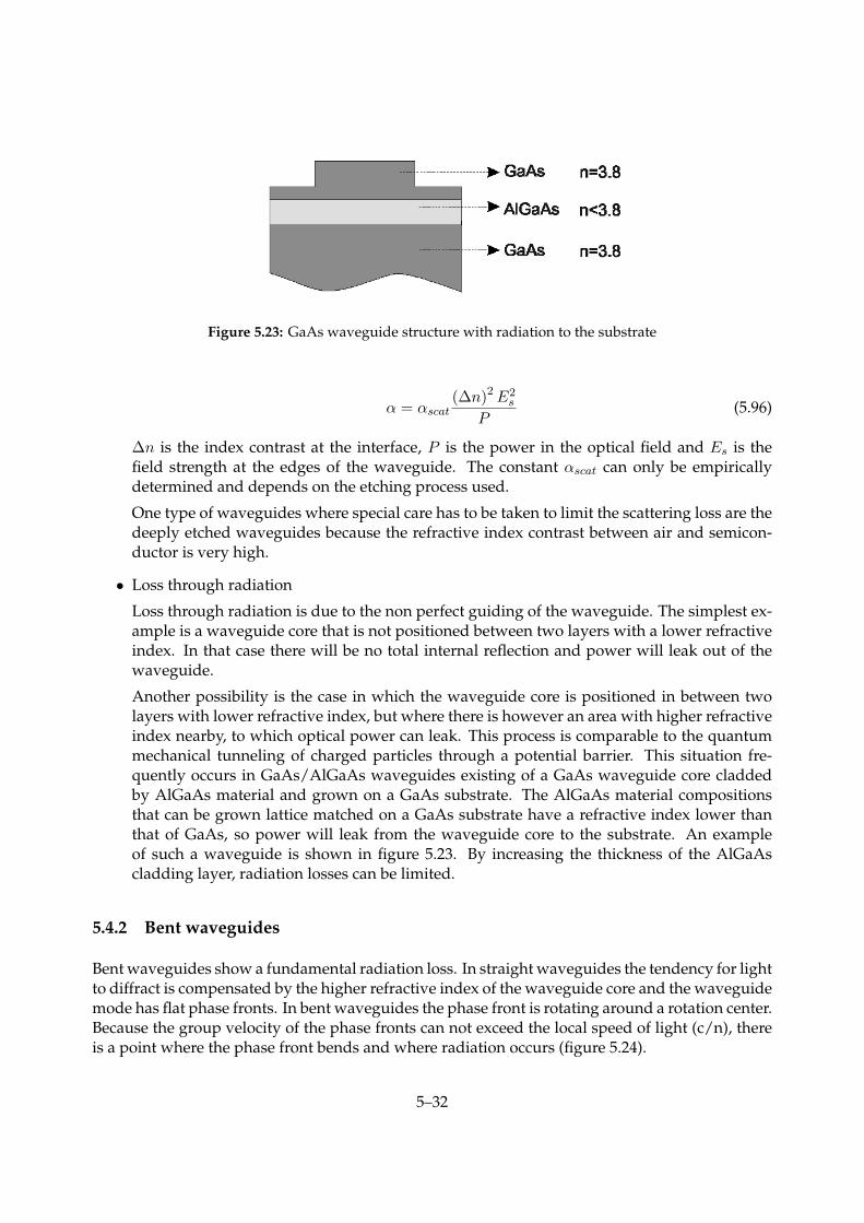
Figure 5.23: GaAs waveguide structure with radiation to the substrate
α = αscat(∆n)2E2
s
P(5.96)
∆n is the index contrast at the interface, P is the power in the optical field and Es is thefield strength at the edges of the waveguide. The constant αscat can only be empiricallydetermined and depends on the etching process used.
One type of waveguides where special care has to be taken to limit the scattering loss are thedeeply etched waveguides because the refractive index contrast between air and semicon-ductor is very high.
• Loss through radiation
Loss through radiation is due to the non perfect guiding of the waveguide. The simplest ex-ample is a waveguide core that is not positioned between two layers with a lower refractiveindex. In that case there will be no total internal reflection and power will leak out of thewaveguide.
Another possibility is the case in which the waveguide core is positioned in between twolayers with lower refractive index, but where there is however an area with higher refractiveindex nearby, to which optical power can leak. This process is comparable to the quantummechanical tunneling of charged particles through a potential barrier. This situation fre-quently occurs in GaAs/AlGaAs waveguides existing of a GaAs waveguide core claddedby AlGaAs material and grown on a GaAs substrate. The AlGaAs material compositionsthat can be grown lattice matched on a GaAs substrate have a refractive index lower thanthat of GaAs, so power will leak from the waveguide core to the substrate. An exampleof such a waveguide is shown in figure 5.23. By increasing the thickness of the AlGaAscladding layer, radiation losses can be limited.
5.4.2 Bent waveguides
Bent waveguides show a fundamental radiation loss. In straight waveguides the tendency for lightto diffract is compensated by the higher refractive index of the waveguide core and the waveguidemode has flat phase fronts. In bent waveguides the phase front is rotating around a rotation center.Because the group velocity of the phase fronts can not exceed the local speed of light (c/n), thereis a point where the phase front bends and where radiation occurs (figure 5.24).
5–32

Figure 5.24: Bent waveguide
Bent waveguides place designers in a dilemma: radiation losses increase nearly exponentiallywith decreasing bend radius. The integration of multiple components on a semiconductor wafer(InP: maximum 2 inch wafers , Silicon: typically 8 inch wafers) requires waveguides that canchange propagation direction on a short distance and without too many losses.
For the theoretical treatment we start off again from a two dimensional waveguide, possibly ob-tained by applying the effective index method. To calculate the waveguide modes we change to acylindrical coordinate system r, φ. The edges of the bent waveguide will coincide with the coordi-nate planes r = R1 and r = R2. In this coordinate system the Helmholtz equation can be writtenas
(∂2
∂r2+
1r
∂
∂r+
1r2
∂2
∂ϕ2+ k2
0n2(r)
)Ψ(r, ϕ) = 0 (5.97)
with n(r) the refractive index profile. We propose a solution
Ψ(r, ϕ) = ψ(r)Φ(ϕ) (5.98)
ψ(r) describes the bend mode profile, while Φ(φ) determines the propagation. Substituting thisequation in the Helmholtz equation results in
(r2
ψ(r)∂2
∂r2+
r
ψ(r)∂
∂r+
r2
ψ(r)k2
0n2(r)
)ψ(r) = − 1
Φ(ϕ)∂2Φ(ϕ)∂ϕ2
(5.99)
5–33

While the left side of equation (5.99) only depends on r and the right side only depends on φ wecan equate both sides with a constant β2
φ. Therefore we can write
1Φ(ϕ)
∂2Φ(ϕ)∂ϕ2
+ β2φ = 0 (5.100)
The general solution to this equation is
Φ(ϕ) = Ce±jβφφ (5.101)
The solution is analogous to the solution for propagation in a straight waveguide. The phase frontscoincide with φ = cte planes. So they turn around the bend. βφ is called the angular propagationconstant (dimension rad−1).
The left side of equation (5.99) can be solved directly by using Bessel functions. This requires thecalculation of Bessel functions with large and complex indices, which leads to a lot of numericalproblems. Another way of solving this equation is the so called conformal transformation. Bysubstituting r = Rte
uRt we can write equation (5.99) like
[∂2
∂u2+ (k2
0n2t (u)− β2
t )]ψ(u) = 0 (5.102)
in which nt(u) = n(u)euRt and βt = βφ
Rt.
This means that in the (u, φ) coordinate system the Helmholtz equation has exactly the same shapeas in a cartesian coordinate system (x, z) when we replace the refractive index profile n(u) bythe transformed index profile nt(u). Modes and propagation constants in bent waveguides cantherefore be calculated by a mode solver developed for solving straight waveguide modes, byintroducing the transformed index profile nt(u). This is schematically depicted in figure 5.25.
Figure 5.26 gives an example of a refractive index profile and the corresponding bend mode profilefor different values of the radius of curvature. Based on the transformed refractive index profile itis easy to understand what happens in a bend:
• From the point where
Re(βt) = nt(u)k0 (5.103)
radiation will occur and the phase front will bend backwards. That way propagation lossesoccur.
• The mode is most strongly guided in the area with the highest refractive index. Therefore,the mode profile will shift towards the outer rim of the bent waveguide. At the transitionfrom straight to bent waveguide mode adaptation losses will occur.
• By decreasing the ring radius, the mode will completely move towards the outer edge ofthe waveguide so that the inner edge of the waveguide does not longer contribute to theguiding of the mode. These modes are called whispering gallery modes. The width of thewaveguide is no longer an issue in the whispering gallery regime.
5–34

Figure 5.25: Conformal transformation
Figure 5.26: Bend mode profiles
5–35

Figure 5.27: Bend mode loss (dB/90 degrees) as a function of radius and refractive index contrast
• By the increased field strength at the outer edge of the waveguide scattering losses will alsoincrease.
These effects are all clearly visible in figure 5.26.
• Radiation losses
Because the refractive index will be larger than the effective index of the waveguide modeat a certain distance from the bend, the effective index of a waveguide bend mode will becomplex. We can write the angular propagation constant as
βφ = β′φ + jαφ (5.104)
and
αφ = αtRt = −Im(neff,t)k0Rt (5.105)
Figure 5.27 shows the attenuation coefficient as a function of the radius and the refractiveindex contrast as a parameter. It is clear that the loss increases rapidly below a certain criticalbend radius.
5–36

Figure 5.28: Adaptations at a straight waveguide / bend waveguide interface
Figure 5.29: BPM calculation of an adiabatic (250um long) and a non-adiabatic (50um long) taper. Bothtapers have a straight input waveguide of 10um long and a straight output waveguide of 100um.
• Mode adaptation losses
In the bend, the mode profile is shifted outwards and is narrower than in the straight waveg-uide. The adaptation losses between straight and bent waveguide can be reduced by reduc-ing the width of the straight waveguide and giving this waveguide an offset with respect tothe bend, such that both waveguide profiles correspond better. The adaptation losses can becalculated by calculating the overlap integral of the bend mode and the mode in the straightwaveguide. An adapted straight waveguide / bend interface is shown in figure 5.28.
5.4.3 Tapers
1. General description
A taper is a smooth transition between two waveguides of different widths or height and isused to couple two components with different waveguide geometry. Changes in the waveg-uide structure result in mode conversion. This means that power is exchanged between thedifferent modes of the waveguide. When power is coupled to radiating modes, loss occurs,but also in the case of multimodal waveguides it is often unwanted that the power is dis-tributed over different waveguide modes. Mode conversion can be suppressed when thechange in waveguide structure is very gentle. In the case we call the adaptation of the modeprofile adiabatic. An adiabatic transition between two waveguide structures is a transitionwhere the mode of the system adapts to the changing geometry without loosing power byconversion to other modes. To analyze taper structures numerical methods need to be used:BPM method or mode expansion and propagation method applied to a staircase approxima-tion of the taper profile.
5–37

Figure 5.30: Definition of the local taper length
Figure 5.31: The linear and parabolic taper
Based on some intuitive considerations it still is possible to derive a criterion to calculate themaximum adiabatic taper angle, which allows an adiabatic transition. As said before, thefundamental mode will transform adiabatically when no power coupling to higher ordermodes occurs. We can assume that especially the coupling to the second order mode isdominant (the first order mode is antisymmetrical). Based on this assumption, we proposethe following criterion for adiabatic transitions: the taper will behave adiabatically when thelocal taper length is larger than the local coupling length between the fundamental mode andthe next symmetrical mode. The local taper length zt is defined as in figure 5.30.
zt =ρ(z)
tan(Ω(z))≈ ρ(z)
Ω(z)(5.106)
The coupling length is given by
zb =π
β0 − β2(5.107)
The criterion then becomes
zt > zb or Ω <
[β0 − β2
π
]ρ (5.108)
Because the difference β0−β2 is proportional to ρ−2 (this will become clear in the discussionon the multimode interference coupler), the maximum taper angle will be larger when thewaveguide is narrower. Therefore, the ideal taper design is parabolic.
2. Improving coupling efficiency to an optical fiber
A typical monomodal optical fiber has a core diameter of 9 µm, has a small refractive indexcontrast between core and cladding layers (∆n ≈ 1%) and the mode is circular. The waveg-
5–38

Figure 5.32: Sections of a directional coupler
uides fabricated in a III-V semiconductor material system typically are a few micrometerwide, have higher refractive index contrast and have non circular mode profiles.
The fundamental modes in the two systems strongly differ, therefore the coupling lossesfrom fiber to waveguide will be high. A possible solution is the use of a taper structure.By narrowing the integrated waveguide (this can be done both transversally or vertically)the mode will expand and a better mode matching can be obtained, thereby reducing thecoupling losses.
5.4.4 Directional coupler
The directional coupler was already treated in previous sections on coupled mode theory andsupermode theory. In these cases always a longitudinally invariant waveguide structure was as-sumed. In reality, a directional coupler consists of a central section (in which the actual couplingtakes place) and an input and output section. In many cases part of the optical power will alreadybe exchanged between the waveguides in the input and output section where the waveguides arealready in close proximity. This needs to be analyzed using the beam propagation method. Themost important application of the directional coupler is the use as a 3dB coupler.
5.4.5 Multimode interference coupler
An alternative to the directional coupler is the use of a multimode interference coupler (MMI). Thecentral part of an MMI is a broad multimode waveguide. Light can be injected in and coupledout of the multimode section through a number of input and output waveguides (figure 5.34).The operation principle of the device is based on the self imaging principle. This is a propertyof multimodal waveguides where an input field is reproduced in single and multiple images atperiodic intervals along the propagation direction of the waveguide. In this way 1xN couplers canbe realized, but also cross couplers and even couplers with an arbitrary coupling ratio.
5–39

Figure 5.33: BPM simulation of a directional coupler. In the upper plots, the intensity profile and theelectrical field profile is shown. The middle graphs show the field distribution at the exit of the directionalcoupler and the refractive index profile of the simulated directional coupler. In the bottom graph the powerin both arms of the coupler is shown. The periodic power exchange is clear.
Figure 5.34: multimode interference coupler
5–40

To gain insight in the operation principle of the MMI, we will use the mode expansion and prop-agation theory. Lets consider the multimodal waveguide of width W which is depicted in figure5.34b. An arbitrary input field Ψ(x, 0) of the MMI can be decomposed in the orthonormal eigen-modes ψi of the MMI.
Ψ(x, 0) =N−1∑i=0
ciψi(x) with ci =∫
Ψ(x, 0)ψi(x)dx (5.109)
In the expansion radiation modes have been neglected, which is acceptable as long as the width ofthe incident field Ψ(x, 0) is sufficiently small compared to the width of the MMI. After propagationover a distance z along the MMI the field becomes
Ψ(x, z) =N−1∑i=0
ciψi(x)e−jβiz = e−jβ0zN−1∑i=0
ciψi(x)ej(β0−βi)z (5.110)
For the modes, the following approximation is made: we assume the shape and propagationconstant of each mode to be given by these of the modes of a waveguide with an infinitely highrefractive index contrast (field is zero at the edges of the waveguide)
ψi(x) = cos(kx,ix) when i is evenψi(x) = sin(kx,ix) when i is oddkx,i = (i+1)π
W
(5.111)
For real waveguide structures this is only an approximation but in the case of high index contrastwaveguides it is a very useful approximation.
As the lateral wave number kx,i and the propagation constant βi are related through
k2x,i + β2
i = k20n
2r (5.112)
we find
βi ≈ k0nr −(i+ 1)2πλ0
4nrW 2(5.113)
Therefore
β0 − βi =i(i+ 2)πλ0
4nrW 2=i(i+ 2)π
3Lπ(5.114)
with
Lπ =π
β0 − β1=
4nrW 2
3λ0(5.115)
5–41
If we substitute this equation into equation (5.110) then we can write down the field in the MMIafter a propagation distance L as (neglecting the common phase term)
Ψ(x, L) =N−1∑i=0
ciψi(x)eji(i+2)π
3LπL (5.116)
From this equation we can deduce some interesting properties of the MMI.
• L = 6LπThen equation (5.116) becomes
Ψ(x, 6Lπ) = Ψ(x, 0) (5.117)
The image at this distance equals the input field
• L = 3LπBecause
ψi(−x) = ψi(x) when i is evenψi(−x) = −ψi(x) when i is odd
(5.118)
we find
Ψ(x, 3Lπ) =N−1∑i=0
ciψi(x)ej[i(i+2)]π
=[N−1∑i=0
ciψi(x)ej[i(i+2)]π
]i=even
+[N−1∑i=0
ciψi(x)ej[i(i+2)]π
]i=odd
=[N−1∑i=0
ciψi(x)]i=even
+[N−1∑i=0−ciψi(x)
]i=odd
=[N−1∑i=0
ciψi(−x)]i=even
+[N−1∑i=0
ciψi(−x)]i=odd
=N−1∑i=0
ciψi(−x)
(5.119)
This means that at a distance 3Lπ the image is the input field, mirrored around the planex = 0.
• L = 3p2Lπ with p odd
After some manipulation we find
Ψ(x, p23Lπ) =N−1∑i=0
ciψi(x)ej[i(i+2)]pπ2
=[N−1∑i=0
ciψi(x)]i=even
+[N−1∑i=0
(−j)pciψi(x)]i=odd
= 1+(−j)p2 Ψ(x, 0) + 1−(−j)p
2 Ψ(−x, 0)(5.120)
5–42

Figure 5.35: BPM simulation of a 1x1 MMI. The dimensions are 15x520 µm2. On the figure the places wheretwo folded (L/2), three folded (L/3,2L/3) and four folded images(L/4,3L/4) are formed, are clearly visible.
Figure 5.36: Y-junction
At this distance we find two images, of which one mirrored, both with amplitude 1/√
2. Soan MMI with this length can be used as a 2x2 3dB coupler.
More general one can show that at the intermediate distances L = 3 pNLπ (with p and N in-
teger numbers without common divider) N multiple images are formed, with an amplitudeof 1√
N. This is illustrated in figure 5.34 and figure 5.35.
5.4.6 Y-junction
The Y-junction is composed of a single waveguide (section A), a taper (section B) and two branchedwaveguides (section C). An important parameter for the Y-junction is the junction angle θ. Whenthe angle is sufficiently small, the fundamental mode will propagate without great losses in bothexit waveguides in section C. This is called an adiabatic Y-junction. The standard Y-junction isdesigned to equally split the input power over both exit waveguides but it is also possible todesign Y-junctions for different splitting ratios.
When we use the Y-junction in the other direction and excite only one branch of the Y-junctionwith the fundamental mode which propagates towards the junction, we can analyze what happensusing the theory of supermodes.
5–43

Figure 5.37: Y-junction used as a combiner
The mode propagating in the lower branch (with amplitude 1) of the Y-junction can be decom-posed into the sum of the local symmetrical and anti-symmetrical supermode each carrying halfof the power (amplitude 1√
2). The symmetrical supermode will adiabatically transform to the fun-
damental mode of the exit waveguide, while the antisymmetric mode will be transformed intothe first order mode. However, when the waveguides are monomodal, this part of the power willradiate. As both super modes carry half of the power, this half is lost. This property can also beexplained based on reciprocity and symmetry of the Y-junction.
In conclusion, we can say that when we use an adiabatically designed Y-junction as a splitter, nolosses occur. When used as a combiner no losses occur when both inputs are excited equally (bothin phase and amplitude). This is the reciprocal situation of the use as a splitter. When only one ofthe inputs is excited, half of the power will be lost and when both inputs are excited equally butin antiphase all power will be lost (for monomodal waveguides).
5.4.7 Diffraction grating
The diffraction grating is analyzed in detail in the chapter on periodic structures. In the integratedversion, the diffraction grating is mostly used as an dispersive element. In this way wavelengthdemultiplexers can be fabricated. Another application is the longitudinal mode selection in a lasercavity. By rotating the diffraction grating a wavelength tunable laser is made.
5.4.8 Phase modulator
Phase modulation in integrated waveguides can be achieved using different physical effects thatinfluence the optical parameters of the material. The most important effects are the electro-opticaleffect, the thermo-optical effect and the influence of free carriers. All these effects create a changein the refractive index of the material which leads to a phase modulation given by
∆φ =2π∆neffL
λ(5.121)
in which L is the length of the waveguide and λ is the operation wavelength.
5–44

5.4.9 Amplifiers
An optical amplifier can be used to boost a signal in a waveguide. The amplifier can for examplebe used in front of a photodetector to reduce the required sensitivity of the photodetector or itcan be used as an in line amplifier for long propagation distances. For this application both adoped optical fiber amplifier (EDFA: Erbium Doped Fiber Amplifier) or an SOA (SemiconductorOptical Amplifier) can be used. Sometimes the amplifier is used to amplify different signals (allat a different wavelength) at the same time. An important issue here is the crosstalk betweendifferent wavelength channel by saturation of the amplifier. A possible solution to this problem isthe so called gain clamped amplifier, where the gain in the amplifier is kept constant.
5.5 Characterization of optical waveguides
Determining the performance of a passive optical waveguide circuit often consists of measuringthe power transmission of the components. A typical measurement setup is shown in figure 5.38.
A light beam from a tunable laser (1) is focused on the right facet of the chip (5) using an opticalfiber (2). The laser spot can be aligned to the waveguides using a micro translation stage (7,8,9)which is often actuated piezo-electrically (11). Part of the laser light will be coupled into thewaveguides. The coupling efficiency is determined by the overlap integral of the laser spot andthe waveguide modes. The coupling efficiency can be increased by using a lensed fiber (4). Aftertransmission through the waveguide light will be coupled out through the left facet and collectedusing an objective lens (6) of which the focus is aligned with the left facet. Using an extra lens (13)this light is focused onto a power meter (15,16). A diafragm (14) makes sure only the light thatcomes from the waveguide is incident on the power meter. When we turn away the power meterit is possible to get a view of the spot with a camera (19,20,21). Polarization can be controlled bypolarization control wheels at the input (3) and a polarization filter (12) at the output. Two othertechniques to couple light in and out of a waveguide are prism coupling and grating assistedcoupling. Grating assisted coupling uses a diffraction grating which is positioned on top of thewaveguide to couple light into the chip.
When we assume that the coupling efficiency into the various waveguides on a chip is equal, wecan this way do relative loss measurements, where different components are compared. Often theloss of the components are measured with the loss of a straight waveguide as a reference.
It is possible to eliminate the coupling efficiency by doing cut-back loss measurements. After aseries of measurements the chip is cleaved in half and one half is used to redo the measurements.The difference between both measurements is the loss in the remaining part. It is clear that thismeasurement technique only works when the coupling efficiencies are equal for both parts.
An alternative way to measure the waveguide losses is the so called Fabry-Perot measurementtechnique. When we couple laser light into a waveguide, reflections occur at the facets which canbe seen as partly reflecting mirrors. By adding the complex wave amplitudes of the subsequentreflections we can calculate the total transmitted power as
T =(1−R)2τ2
(1− τ2R)2 + 4τ2R sin2(βL)with τ2 = e−αL (5.122)
5–45

Figure 5.38: Measurement setup
Figure 5.39: Fabry-Perot resonances in a waveguide
This transmission function is wavelength dependent (through the propagation constant β). Whenwe calculate the ratio Tmax
Tminwe find that
S =Tmax
Tmin=
(1 + τ2R)2
(1− τ2R)2(5.123)
This way we can calculate the attenuation as
αdB =10L
(log(R)− log(√S − 1√S + 1
))[dB/cm] (5.124)
By measuring the transmitted power as a function of wavelength we can easily determine theratio Tmax
Tmin. When we know the reflection coefficientR (typically 0.32 for waveguide in InP) we can
determine the attenuation coefficient of the waveguide. For a correct measurement it is necessaryhowever that only one mode is excited. In figure 5.40 two examples of this type of measurementsare given. For the first measurement the determination of the ratio S is simple. For the secondmeasurement an unambiguous measurement is impossible. There are many possible causes for
5–46

Figure 5.40: Fabry-Perot loss measurements
Figure 5.41: Double perturbed waveguide system
this problem: parasitic reflections in the measurement setup, vibrations, multimodal excitation,wavelength dependence of the focal distance between facet and objective lens...
5.6 Appendix
5.6.1 Calculation of the coupling coefficients κi,j for a directional coupler
For the uncoupled waveguides with respective index profile n1(x) and n2(x) we can write
∂2ϕ1(x)∂x2 + (k2
0n21(x)− β2
1)ϕ1(x) = 0∂2ϕ2(x)∂x2 + (k2
0n22(x)− β2
2)ϕ2(x) = 0(5.125)
For the field in the coupled waveguides we can write
∂2Ψ(x, z)∂x2
+∂2Ψ(x, z)∂z2
+ k20n
212(x)Ψ(x, z) = 0 (5.126)
If we propose following solution for Ψ(x, z)
5–47

Ψ(x, z) = C1(z)ϕ1(x)e−jβ1z + C2(z)ϕ2(x)e−jβ2z (5.127)
in which C1 and C2 slowly vary with z so that we can assume
∣∣∣∣∂2Ci∂z2
∣∣∣∣ << ∣∣∣∣−jβi∂Ci∂z
∣∣∣∣ (5.128)
Substituting equation (5.127) into equation (5.126) and taking equation (5.128) into account, wefind that
[∂2ϕ1(x)∂x2 + (k2
0n212(x)− β2
1)ϕ1(x)]C1e
−jβ1z − 2jβ1ϕ1(x)dC1dz e
−jβ1z
+[∂2ϕ2(x)∂x2 + (k2
0n212(x)− β2
2)ϕ2(x)]C2e
−jβ2z − 2jβ2ϕ2(x)dC2dz e
−jβ2z = 0(5.129)
When we use equation (5.125), this becomes
k20
[n2
12(x)− n21
]ϕ1(x)C1e
−jβ1z − j2β1ϕ1(x)dC1dz e
−jβ1z
+k20
[n2
12(x)− n22
]ϕ2(x)C2e
−jβ2z − j2β2ϕ2(x)dC2dz e
−jβ2z = 0(5.130)
When the eigenmodes are orthonormal
βi
∫ϕi(x)ϕj(x)dx = δij (5.131)
we find that (by multiplying equation (5.130) with ϕ1 and integrating over x):
dC1
dze−jβ1z = −jκ11C1e
−jβ1z − jκ12C2e−jβ2z (5.132)
and by multiplying equation (5.130) with ϕ2 and integrating over x:
dC2
dze−jβ2z = −jκ22C2e
−jβ2z − jκ21C1e−jβ1z (5.133)
with
κ11 = 12k
20
∫(n2
12 − n21)ψ2
1dxκ12 = 1
2k20
∫(n2
12 − n21)ψ1ψ2dx
κ21 = 12k
20
∫(n2
12 − n22)ψ1ψ2dx
κ22 = 12k
20
∫(n2
12 − n22)ψ2
2dx
(5.134)
When
X1(z) = C1(z)e−jβ1z
X2(z) = C2(z)e−jβ2z (5.135)
5–48

equation (5.132) and (5.133) become
dX1dz = −jβ1X1 − j(κ11X1 + κ12X2)dX2dz = −jβ2X2 − j(κ21X1 + κ22X2)
(5.136)
These are the equations proposed by the coupled mode theory.
5–49