Embed Size (px)
Citation preview
Different threshold and bipolar resistive switching mechanisms in reactively sputteredamorphous undoped and Cr-doped vanadium oxide thin filmsJonathan A. J. Rupp, Madec Querré, Andreas Kindsmüller, Marie-Paule Besland, Etienne Janod, ReginaDittmann, Rainer Waser, and Dirk J. Wouters
Citation: Journal of Applied Physics 123, 044502 (2018); doi: 10.1063/1.5006145View online: https://doi.org/10.1063/1.5006145View Table of Contents: http://aip.scitation.org/toc/jap/123/4Published by the American Institute of Physics
Articles you may be interested inEffect of thermal insulation on the electrical characteristics of NbOx threshold switchesApplied Physics Letters 112, 073102 (2018); 10.1063/1.5015941
A metal-insulator transition study of VO2 thin films grown on sapphire substratesJournal of Applied Physics 122, 235102 (2017); 10.1063/1.4997437
NbOx based oscillation neuron for neuromorphic computingApplied Physics Letters 111, 103503 (2017); 10.1063/1.4991917
Analysis of the threshold switching mechanism of a Te–SbO selector device for crosspoint nonvolatile memoryapplicationsApplied Physics Letters 111, 183501 (2017); 10.1063/1.4998493
Light-activated resistance switching in SiOx RRAM devicesApplied Physics Letters 111, 233502 (2017); 10.1063/1.5009069
Irreversible metal-insulator transition in thin film VO2 induced by soft X-ray irradiationApplied Physics Letters 111, 241605 (2017); 10.1063/1.5012940
Different threshold and bipolar resistive switching mechanisms in reactivelysputtered amorphous undoped and Cr-doped vanadium oxide thin films
Jonathan A. J. Rupp,1,a) Madec Querr�e,2 Andreas Kindsm€uller,1 Marie-Paule Besland,2
Etienne Janod,2 Regina Dittmann,3 Rainer Waser,1,3 and Dirk J. Wouters1,a)
1Institut f€ur Werkstoffe der Elektrotechnik II (IWE II), RWTH Aachen, Sommerfeldstraße 24, 52072 Aachen,Germany2Institut des Mat�eriaux Jean Rouxel (IMN), Universit�e de Nantes, CNRS, 2 rue de la Houssiniere, BP 32229,44322 Nantes Cedex 3, France3Forschungszentrum, J€ulich PGI-7, 42425 J€ulich, Germany
(Received 22 September 2017; accepted 17 December 2017; published online 24 January 2018)
This study investigates resistive switching in amorphous undoped and Cr-doped vanadium oxide
thin films synthesized by sputtering deposition at low oxygen partial pressure. Two different vola-
tile threshold switching characteristics can occur as well as a non-volatile bipolar switching mecha-
nism, depending on device stack symmetry and Cr-doping. The two threshold switching types are
associated with different crystalline phases in the conduction filament created during an initial
forming step. The first kind of threshold switching, observed for undoped vanadium oxide films,
was, by its temperature dependence, proven to be associated with a thermally triggered insulator-
to-metal transition in a crystalline VO2 phase, whereas the threshold switch observed in chromium
doped films is stable up to 90 �C and shows characteristics of an electronically induced Mott transi-
tion. This different behaviour for undoped versus doped films has been attributed to an increased
stability of V3þ due to the Cr3þ doping (as evidenced by X-ray photoelectron spectroscopy analy-
sis), probably favouring the creation of a crystalline Cr-doped V2O3 phase (rather than a Cr-doped
VO2 phase) during the energetic forming step. The symmetric Pt/a-(VCr)Ox/Pt device showing
high temperature stable threshold switching may find interesting applications as a possible new
selector device for resistive switching memory (ReRAM) crossbar arrays. Published by AIPPublishing. https://doi.org/10.1063/1.5006145
I. INTRODUCTION
Electrically induced resistive switching phenomena, in
particular in metal oxides, are of strong interest to develop
novel devices enabling new types of memories and logic.
Amongst many transition metal oxides that are subject of
ongoing explorations, the complex material class of vana-
dium oxides spans a broad range with over 20 stable phases1
which possess remarkable electrical switching properties.
Most of the crystalline Magn�eli VnO2n-1 and Wadsley
VnO2nþ1 phases show an Insulator-to-Metal transition
(IMT)2 below room temperature, while to our present
knowledge there are only two well-established phases with
an IMT above room temperature, namely VO2 at 68 �C3 and
V3O5 at 155 �C.4 In the last decade, extensive research was
carried out to exploit the electrical switching ability of VO2
as a selector.5 However, its applicability appeared seriously
limited by its low transition temperature.6 In addition, it has
been shown that increasing Cr-content up to 11 at. % allows
an increase of the IMT temperature of VO2 by only about
11 �C.7 An alternative is the use of NbO2 with a much higher
IMT temperature where the threshold switching was recently
related to an electronic process rather than to the thermally
triggered IMT itself.8 Moreover, the Cr-doped V2O3 phase is
well known as the archetype of Mott insulators,9 in which an
electric-field-driven volatile resistive switching can be
established by triggering of the Mott transition via an elec-
tronic (avalanche breakdown) mechanism.10 Apart from
these specific IMT- and Mott-phase associated resistive
change phenomena, we may expect a non-volatile resistive
switching mechanism based on a valence change (VCM) by
the drift of oxygen vacancies, which is a general observed
process in transition metal oxides.11 All mentioned mecha-
nisms can in theory take place in Cr-doped vanadium oxides
depending on which conditions and crystalline phases come
into play. In this paper, we report on a systematic investiga-
tion of the switching behaviour of low oxygen content (V:O
� 2:3, i.e., close to V2O3) amorphous VOx and (V,Cr)Ox thin
films deposited by reactive physical vapor deposition process
(PVD) using both symmetric and asymmetric metal-insula-
tor-metal (MIM) structures. We show that, after an energetic
forming process, different threshold and bipolar resistive
switching (BRS) mechanisms occur depending on the mate-
rial (Cr doped or undoped) and choice of the electrode
material (Pt or V top electrode). These results might be
understood by the formation of different crystalline material
phases within a switching filament.
II. EXPERIMENTAL DETAILS
Amorphous undoped and Cr-doped VOx films with a
thickness of 90 nm have been deposited by reactive RF mag-
netron sputtering at room temperature with a growth rate of
6.3 nm/min. A one inch metallic vanadium target was useda)[email protected] and [email protected]
0021-8979/2018/123(4)/044502/9/$30.00 Published by AIP Publishing.123, 044502-1
JOURNAL OF APPLIED PHYSICS 123, 044502 (2018)
with a power of PV¼100 W, while (for the Cr-doped films) Cr
was co-sputtered (with a power of PCr¼5–10 W) from a one
inch metallic Cr-target. The distance between target and sub-
strate constituted 5 cm. As determined by X-ray Photoelectron
Spectroscopy (XPS) measurements, the Cr- doping level was
3 at. % Cr for 5 W and 10 at. % for 10 W sputter power—(see
supplementary material Table S1). The base pressure was
held below pbase<1 nbar and the process pressure was fixed at
pprocess¼10 lbar. The oxygen flow was introduced close to the
target. Hereby, the oxygen partial pressure p(O2) was adjusted
by the flux ratio of two mass flow controllers: one with pure
argon (90 sccm) and one with a mixture of argon and oxygen
in the ratio 99:1 (10 sccm). This allowed the control of the
p(O2) in a few 10 nbar range. The relatively low oxygen par-
tial pressure value of 10 nbar was used to target a V:O ratio in
the amorphous film close to 2:3. Indeed, a separate (unpub-
lished) study by the authors of the deposition of crystalline
(Cr)VOx films at high temperature up to 600 �C showed the
desired V2O3 phase at this pressure. High-temperature depos-
ited crystalline films were also used as XPS reference sam-
ples. Thin film morphology was investigated by Scanning
Electron Microscopy (SEM) with a Zeiss “DSM982
GEMINI;” roughness of thin films was calculated out of
1� 1 lm2 area scans using Atomic Force Microscopy (AFM)
measurements performed with a Veeco “di CP II”. Density
and thickness of thin films were extracted from the X-ray
Reflectivity (XRR) measurements obtained with an X-Ray
Diffractometer from PANalytical “X’Pert PRO”. The different
oxidation states of thin films were determined from XPS
analysis using a “PHI 5000 Versa Probe II” of Ulvac-Phi, Inc.
XRR fitting was performed by PANalytical’s “X’pert
Reflectometry” and XPS fitting by “CasaXPS” v2.3.17.
Crystallinity was probed by X-ray diffraction in surface sensi-
tive grazing incidence mode (XRD-GI).
For all analysis, undoped and Cr-doped VOx films were
deposited on a 30 nm thick Pt electrode on SiO2/Si substrates
with a 5 nm Ti sticking layer in between SiO2 and Pt. To pre-
vent layer oxidation of samples for XPS analysis, films were
capped in situ with 50 nm of sputtered Au and transported to
the XPS system where the Au cap was removed inside the
vacuum system just before analysis. Study of the resistive
switching properties of amorphous undoped and Cr-doped
VOx thin films was performed by using symmetric as well as
asymmetric MIM devices (Figs. 3 and 4). For MIM devices,
a 100 nm thick Pt or a stacked (50 nm V/50 nm Pt) electrode
was used on top of (V,Cr)Ox thin films. Devices were pat-
terned by UV-lithography and lift-off processes.
Electrical characterization was performed by quasistatic
I–V measurements from room temperature up to 90 �C on
10� 10 lm2 and 25� 25 lm2 pads which showed similar
behaviour. Here, we report on 25� 25 lm2 devices. The
voltage was imposed on the top electrode whereas the bot-
tom electrode was held on ground potential.
III. RESULTS
A. Layer morphology
As a representative example for all investigated amor-
phous layers, SEM, AFM and fitted XRR-analysis for
undoped and Cr-doped low oxygen content (V:O� 2:3) VOx
films are given in Fig. 1 and Table I.
As displayed, the undoped VOx film exhibits a porous
microstructure [Fig. 1(a)] with a random grain orientation in
cross section [Fig. 1(b)] and a density of 4.0 g/cm3, calculated
by XRR-fitting (Table I). In contrast, the Cr-doped layer/films
(V,Cr)Ox show a denser and vertically aligned columnar struc-
ture where some grain edges emerge out of the surface plane
[Fig. 1(d)] and with low inter-columnar spaces [Fig. 1(e)]. The
higher density is supported by a higher XRR-fitted density of
4.4 g/cm3 (Table I). The mean square roughness extracted from
AFM images [Figs. 1(c) and 1(f)] and XRR-fitting (Table I) is
similar in the 1.3 to 1.5 nm range for both samples.
B. Oxidation state
To evaluate the oxidation states of amorphous layers,
XPS spectra of V2p core level spectra were measured for
both undoped and 10 at. % Cr-doped VOx sputtered amor-
phous thin films (Fig. 2). The relatively high Cr-content was
FIG. 1. SEM plan view and cross section images of 90 nm thick VOx [(a)
and (b)] and (V0.97Cr0.03)Ox [(d) and (e)] thin films deposited on 30 nm Pt.
One can see the same surface roughness but an oriented columnar grain
growth and a higher density for Cr-doped VOx. Bottom part: Topography of
VOx (c) and (V0.97Cr0.03)Ox (f) thin films determined by AFM with rough-
ness as false color scale.
TABLE I. Thickness d, density q, and mean square roughness Rms extracted
from XRR/AFM measurements and fit data.
Material d (nm) q (g/cm3) Rms (nm) (XRR) Rms (nm)(AFM)
VOx 8962 4.060.1 1.560.1 1.360.2
VCrOx 9061 4.460.1 1.360.1 1.260.2
044502-2 Rupp et al. J. Appl. Phys. 123, 044502 (2018)
chosen to ensure a reasonable sensitivity for the Cr-
detection. To fit the data, in addition to literature compari-
son,12–14 crystalline samples of V, VO, V2O3, VO2, and
V2O5 were synthesized where oxidation states betweenþ0
andþ5 (þ1 excluded) could be extracted. These V2p-binding
energies were henceforth taken as reference. Table II sum-
marizes binding energy positions, associated with each oxi-
dation state and used to fit experimental data, as well as
integral peak areas of the oxidation states for both samples.
As displayed in Fig. 2, in both cases, every peak of V2p
core level can be decomposed into three elementary compo-
nents which can be associated with the different oxidation states
of vanadium. Starting from lower binding energy, peaks attrib-
uted to V3þ, V4þ, and V5þ oxidation states should be involved
to fully fit the recorded spectra. Thus, both samples contain a
mix of vanadium valences betweenþ3 andþ5 with a major
contribution of V4þ at 516.1 eV for the V2p 3/2 peak. In the
case of undoped vanadium oxide film, the contributions of V3þ
and V5þ are quite similar (29% and 22%, respectively, as
displayed in Table II), whereas for the Cr-doped sample the
contribution of V3þ significantly increases in comparison to the
undoped layer by a factor of 1.5 from 29% to 45% [shown in
detail at V2p 3/2 in Fig. 2(c)]. For the Cr-doped layer, the V3þ
and V4þ contributions are close together while the V5þ compo-
nent is less significant at 14%. Considering the Cr 2p core level,
chromium appears only oxidized in Cr3þ valence [Fig. 2(d)].
C. Electrical characterization
At first, undoped VOx devices with symmetric Pt-
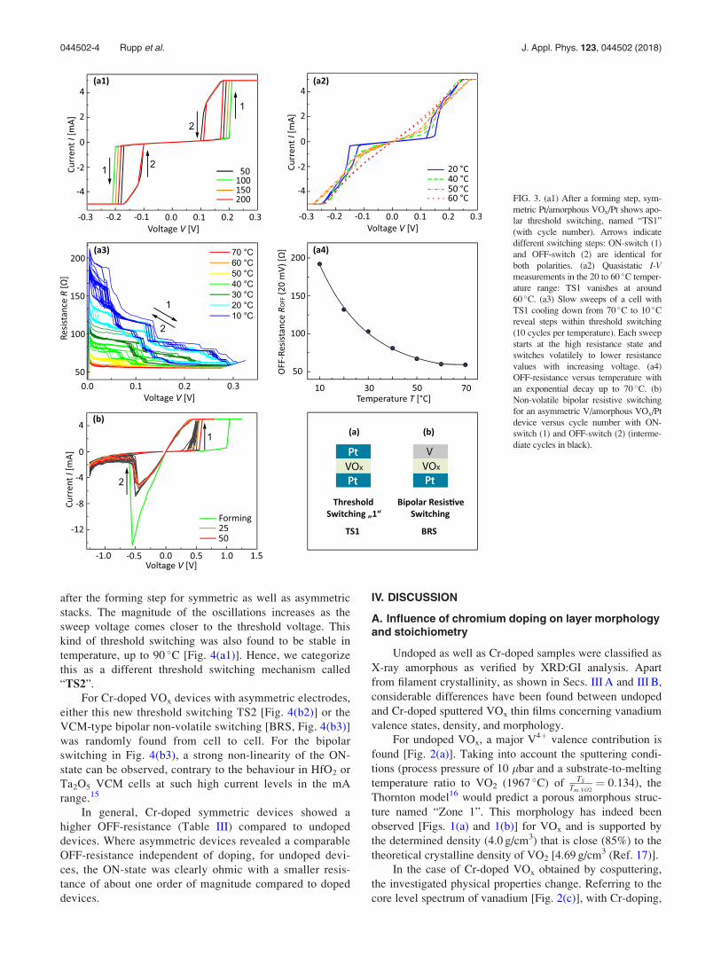
electrodes were investigated [Fig. 3(a)]. After a forming step
(at high voltage and current of at least 7 V and 4 mA, respec-
tively), an apolar volatile threshold switch could be created
independently of the applied polarity [Fig. 3(a1)]. The
threshold voltage VON varied with cycling between 0.1 V up
to a maximum voltage of 0.4 V (here shown up to 0.25 V).
For temperature dependent I-V sweeps, the threshold van-
ished at 60 �C [Fig. 3(a2)]. Such a threshold switch with a
broad hysteresis loop is hereby named “TS1”. In Fig. 3(a3),
TS1 was formed in a cell at room temperature and afterwards
heated up to 70 �C. Then, the pad was cycled with a slow
measurement speed in 10 �C steps while cooling down to
10 �C. The OFF-resistance (measured at constant voltage of
20 mV) increased exponentially from 60 �C downwards [as
seen in Fig. 3(a4)] and discrete volatile resistance jumps
started to form in the R-V sweeps. The lower the tempera-
ture, the more steps were observed. Figure 3(b) depicts I-Vsweeps of an undoped and asymmetric VOx device with
vanadium as top electrode, which after forming (at a lower
voltage of �1 V than symmetric cells) mainly showed bipo-
lar resistive switching (BRS). In very rare cases, asymmetric
stacks also showed threshold switching as well as symmetric
stacks showed BRS.
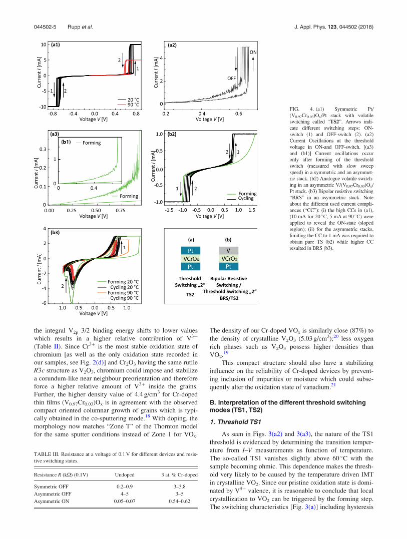
Further, symmetric and asymmetric devices with 3 at. %
Cr-doped VOx films were investigated (Fig. 4). For symmet-
ric devices Pt/(V0.97Cr0.03)Ox/Pt [Fig. 4(a)], it was not possi-
ble to induce TS1 or any non-volatile switching. However, a
threshold switching, very different from the TS1 of undoped
VOx films, is systematically observed [Fig. 4(a1)]. Already
its forming voltage and current (2.5 V/ less than 1 mA) are
indeed lower than for undoped VOx (7 V/ 4 mA). Moreover,
the threshold occurred at much higher voltage than TS1 (for
voltages above 0.6 V instead of 0.25 V for TS1), with narrow
or vanishing hysteresis (VOFF being very close to VON) and
without any intermediate steps as shown for the symmetric
undoped stack in Fig. 3(a3). Rather, at voltages just before
the ON- and after the OFF-switch, the current oscillates right
at the transition from high to low resistive state and vice
versa [Fig. 4(a2)]. Figures 4(a3) and 4(b1) show these oscil-
lations (within a slow sweep speed) becoming active right
FIG. 2. Vanadium V2p core level spectra of amorphous VOx (a) and (V0.9Cr0.1)Ox (b), sputtered at 10 nbar oxygen partial pressure at room temperature.
(c) Comparison of V2p 3/2 peaks recorded for VOx and (VCr)Ox and (d) core level spectra of Chromium Cr 2p.
TABLE II. Binding energies and integral peak area for vanadium 2p 3/2 oxi-
dation statesþ3þ 4 andþ5 in amorphous VOx and (V0.9Cr0.1)Ox.
Oxidation state of vanadium þ3 þ4 þ5
Binding energy EB (eV) 515.060.3 516.260.2 517.360.2
Integral peak area (%) undoped 29 49 22
Integral peak area (%) Cr-doped 45 41 14
044502-3 Rupp et al. J. Appl. Phys. 123, 044502 (2018)
after the forming step for symmetric as well as asymmetric
stacks. The magnitude of the oscillations increases as the
sweep voltage comes closer to the threshold voltage. This
kind of threshold switching was also found to be stable in
temperature, up to 90 �C [Fig. 4(a1)]. Hence, we categorize
this as a different threshold switching mechanism called
“TS2”.
For Cr-doped VOx devices with asymmetric electrodes,
either this new threshold switching TS2 [Fig. 4(b2)] or the
VCM-type bipolar non-volatile switching [BRS, Fig. 4(b3)]
was randomly found from cell to cell. For the bipolar
switching in Fig. 4(b3), a strong non-linearity of the ON-
state can be observed, contrary to the behaviour in HfO2 or
Ta2O5 VCM cells at such high current levels in the mA
range.15
In general, Cr-doped symmetric devices showed a
higher OFF-resistance (Table III) compared to undoped
devices. Where asymmetric devices revealed a comparable
OFF-resistance independent of doping, for undoped devi-
ces, the ON-state was clearly ohmic with a smaller resis-
tance of about one order of magnitude compared to doped
devices.
IV. DISCUSSION
A. Influence of chromium doping on layer morphologyand stoichiometry
Undoped as well as Cr-doped samples were classified as
X-ray amorphous as verified by XRD:GI analysis. Apart
from filament crystallinity, as shown in Secs. III A and III B,
considerable differences have been found between undoped
and Cr-doped sputtered VOx thin films concerning vanadium
valence states, density, and morphology.
For undoped VOx, a major V4þ valence contribution is
found [Fig. 2(a)]. Taking into account the sputtering condi-
tions (process pressure of 10 lbar and a substrate-to-melting
temperature ratio to VO2 (1967 �C) of TS
Tm;VO2¼ 0:134), the
Thornton model16 would predict a porous amorphous struc-
ture named “Zone 1”. This morphology has indeed been
observed [Figs. 1(a) and 1(b)] for VOx and is supported by
the determined density (4.0 g/cm3) that is close (85%) to the
theoretical crystalline density of VO2 [4.69 g/cm3 (Ref. 17)].
In the case of Cr-doped VOx obtained by cosputtering,
the investigated physical properties change. Referring to the
core level spectrum of vanadium [Fig. 2(c)], with Cr-doping,
FIG. 3. (a1) After a forming step, sym-
metric Pt/amorphous VOx/Pt shows apo-
lar threshold switching, named “TS1”
(with cycle number). Arrows indicate
different switching steps: ON-switch (1)
and OFF-switch (2) are identical for
both polarities. (a2) Quasistatic I-Vmeasurements in the 20 to 60 �C temper-
ature range: TS1 vanishes at around
60 �C. (a3) Slow sweeps of a cell with
TS1 cooling down from 70 �C to 10 �Creveal steps within threshold switching
(10 cycles per temperature). Each sweep
starts at the high resistance state and
switches volatilely to lower resistance
values with increasing voltage. (a4)
OFF-resistance versus temperature with
an exponential decay up to 70 �C. (b)
Non-volatile bipolar resistive switching
for an asymmetric V/amorphous VOx/Pt
device versus cycle number with ON-
switch (1) and OFF-switch (2) (interme-
diate cycles in black).
044502-4 Rupp et al. J. Appl. Phys. 123, 044502 (2018)
the integral V2p 3/2 binding energy shifts to lower values
which results in a higher relative contribution of V3þ
(Table II). Since Cr3þ is the most stable oxidation state of
chromium [as well as the only oxidation state recorded in
our samples, see Fig. 2(d)] and Cr2O3 having the same rutile
R3c structure as V2O3, chromium could impose and stabilize
a corundum-like near neighbour preorientation and therefore
force a higher relative amount of V3þ inside the grains.
Further, the higher density value of 4.4 g/cm3 for Cr-doped
thin films (V0.97Cr0.03)Ox is in agreement with the observed
compact oriented columnar growth of grains which is typi-
cally obtained in the co-sputtering mode.18 With doping, the
morphology now matches “Zone T” of the Thornton model
for the same sputter conditions instead of Zone 1 for VOx.
The density of our Cr-doped VOx is similarly close (87%) to
the density of crystalline V2O3 (5.03 g/cm3);20 less oxygen
rich phases such as V2O3 possess higher densities than
VO2.19
This compact structure should also have a stabilizing
influence on the reliability of Cr-doped devices by prevent-
ing inclusion of impurities or moisture which could subse-
quently alter the oxidation state of vanadium.21
B. Interpretation of the different threshold switchingmodes (TS1, TS2)
1. Threshold TS1
As seen in Figs. 3(a2) and 3(a3), the nature of the TS1
threshold is evidenced by determining the transition temper-
ature from I–V measurements as function of temperature.
The so-called TS1 vanishes slightly above 60 �C with the
sample becoming ohmic. This dependence makes the thresh-
old very likely to be caused by the temperature driven IMT
in crystalline VO2. Since our pristine oxidation state is domi-
nated by V4þ valence, it is reasonable to conclude that local
crystallization to VO2 can be triggered by the forming step.
The switching characteristics [Fig. 3(a)] including hysteresis
FIG. 4. (a1) Symmetric Pt/
(V0.97Cr0.03)Ox/Pt stack with volatile
switching called “TS2”. Arrows indi-
cate different switching steps: ON-
switch (1) and OFF-switch (2). (a2)
Current Oscillations at the threshold
voltage in ON-and OFF-switch. [(a3)
and (b1)] Current oscillations occur
only after forming of the threshold
switch (measured with slow sweep
speed) in a symmetric and an asymmet-
ric stack. (b2) Analogue volatile switch-
ing in an asymmetric V/(V0.97Cr0.03)Ox/
Pt stack. (b3) Bipolar resistive switching
“BRS” in an asymmetric stack. Note
about the different used current compli-
ances (“CC”): (i) the high CCs in (a1),
(10 mA for 20 �C, 5 mA at 90 �C) were
applied to reveal the ON-state (sloped
region); (ii) for the asymmetric stacks,
limiting the CC to 1 mA was required to
obtain pure TS (b2) while higher CC
resulted in BRS (b3).
TABLE III. Resistance at a voltage of 0.1 V for different devices and resis-
tive switching states.
Resistance R (kX) (0.1V) Undoped 3 at. % Cr-doped
Symmetric OFF 0.2–0.9 3–3.8
Asymmetric OFF 4–5 3–5
Asymmetric ON 0.05–0.07 0.54–0.62
044502-5 Rupp et al. J. Appl. Phys. 123, 044502 (2018)
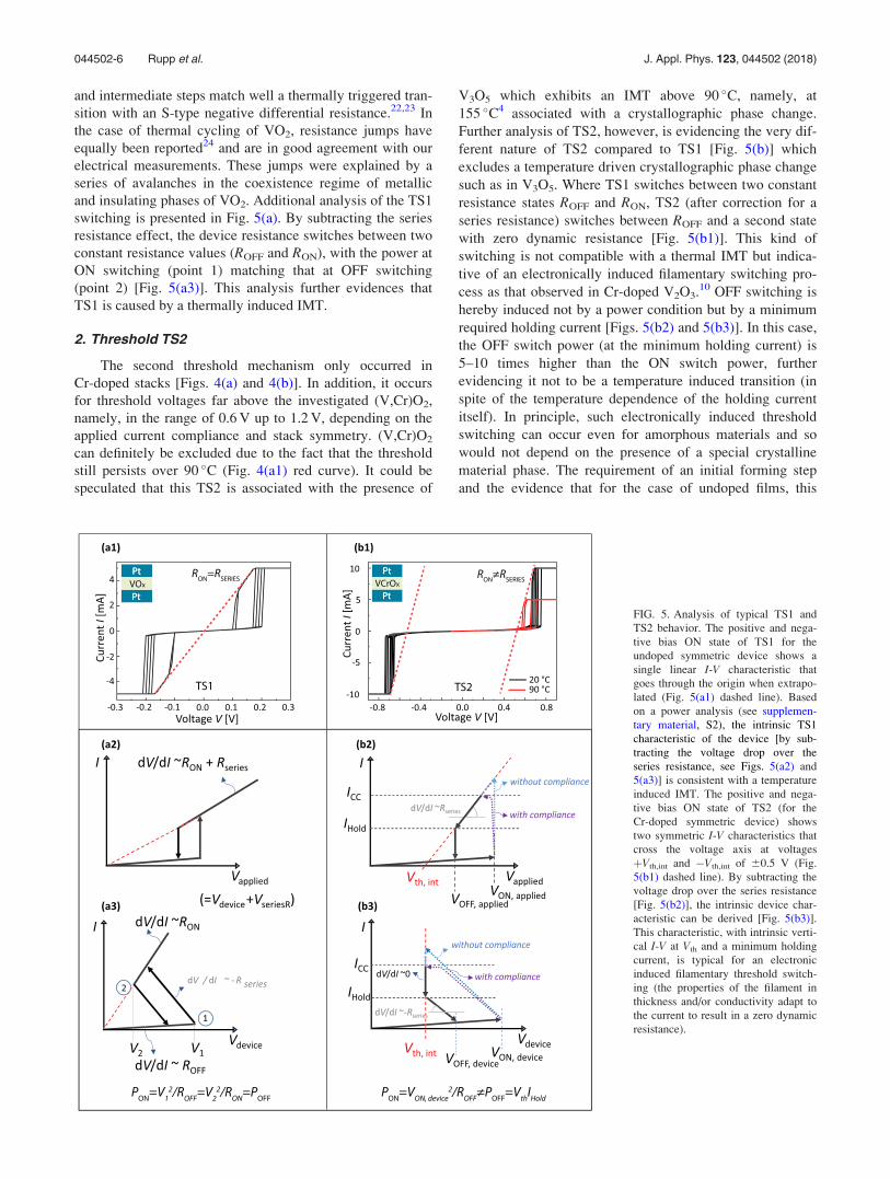
and intermediate steps match well a thermally triggered tran-
sition with an S-type negative differential resistance.22,23 In
the case of thermal cycling of VO2, resistance jumps have
equally been reported24 and are in good agreement with our
electrical measurements. These jumps were explained by a
series of avalanches in the coexistence regime of metallic
and insulating phases of VO2. Additional analysis of the TS1
switching is presented in Fig. 5(a). By subtracting the series
resistance effect, the device resistance switches between two
constant resistance values (ROFF and RON), with the power at
ON switching (point 1) matching that at OFF switching
(point 2) [Fig. 5(a3)]. This analysis further evidences that
TS1 is caused by a thermally induced IMT.
2. Threshold TS2
The second threshold mechanism only occurred in
Cr-doped stacks [Figs. 4(a) and 4(b)]. In addition, it occurs
for threshold voltages far above the investigated (V,Cr)O2,
namely, in the range of 0.6 V up to 1.2 V, depending on the
applied current compliance and stack symmetry. (V,Cr)O2
can definitely be excluded due to the fact that the threshold
still persists over 90 �C (Fig. 4(a1) red curve). It could be
speculated that this TS2 is associated with the presence of
V3O5 which exhibits an IMT above 90 �C, namely, at
155 �C4 associated with a crystallographic phase change.
Further analysis of TS2, however, is evidencing the very dif-
ferent nature of TS2 compared to TS1 [Fig. 5(b)] which
excludes a temperature driven crystallographic phase change
such as in V3O5. Where TS1 switches between two constant
resistance states ROFF and RON, TS2 (after correction for a
series resistance) switches between ROFF and a second state
with zero dynamic resistance [Fig. 5(b1)]. This kind of
switching is not compatible with a thermal IMT but indica-
tive of an electronically induced filamentary switching pro-
cess as that observed in Cr-doped V2O3.10 OFF switching is
hereby induced not by a power condition but by a minimum
required holding current [Figs. 5(b2) and 5(b3)]. In this case,
the OFF switch power (at the minimum holding current) is
5–10 times higher than the ON switch power, further
evidencing it not to be a temperature induced transition (in
spite of the temperature dependence of the holding current
itself). In principle, such electronically induced threshold
switching can occur even for amorphous materials and so
would not depend on the presence of a special crystalline
material phase. The requirement of an initial forming step
and the evidence that for the case of undoped films, this
FIG. 5. Analysis of typical TS1 and
TS2 behavior. The positive and nega-
tive bias ON state of TS1 for the
undoped symmetric device shows a
single linear I-V characteristic that
goes through the origin when extrapo-
lated (Fig. 5(a1) dashed line). Based
on a power analysis (see supplemen-
tary material, S2), the intrinsic TS1
characteristic of the device [by sub-
tracting the voltage drop over the
series resistance, see Figs. 5(a2) and
5(a3)] is consistent with a temperature
induced IMT. The positive and nega-
tive bias ON state of TS2 (for the
Cr-doped symmetric device) shows
two symmetric I-V characteristics that
cross the voltage axis at voltages
þVth,int and �Vth,int of 60.5 V (Fig.
5(b1) dashed line). By subtracting the
voltage drop over the series resistance
[Fig. 5(b2)], the intrinsic device char-
acteristic can be derived [Fig. 5(b3)].
This characteristic, with intrinsic verti-
cal I-V at Vth and a minimum holding
current, is typical for an electronic
induced filamentary threshold switch-
ing (the properties of the filament in
thickness and/or conductivity adapt to
the current to result in a zero dynamic
resistance).
044502-6 Rupp et al. J. Appl. Phys. 123, 044502 (2018)
results in the formation of a crystalline (VO2) phase, how-
ever, strongly suggest that also here we probably form a
crystalline phase, which then cannot stem from a phase
showing a thermal IMT as VO2. In addition, the strong
current oscillations jumping back and forth (right at the
threshold voltage) can be explained by a metastable conduc-
tive filament as result of an electronically induced Mott-
transition.10 There, a persisting competition arises between
an electrically triggered conductive path and—by associated
Joule heating—a thermally induced relaxation of metallic
domains to an insulating state. This is in strong contrast to a
Joule-heating driven transition to a conductive state in VO2
(or V3O5) with each conductive jump arising one after the
other solely towards further ON-switch (increasing voltage)
or further OFF-switch (decreasing voltage).
For these reasons, we clearly favour the explanation
according to which TS2 is related to the presence of a crys-
talline (V0.97Cr0.03)2O3 Mott phase.
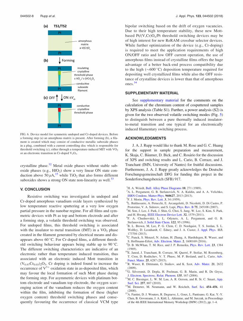
C. Device model
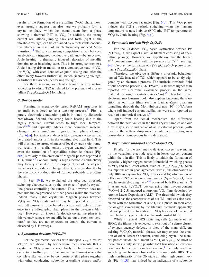
Forming in metal-oxide based ReRAM structures is
generally considered to be a two-step process.25 First, a
purely electronic conduction path is initiated by dielectric
breakdown. Second, the strong Joule heating due to the
highly localized current leads to high local tempera-
tures26,27 and typically induces more permanent material
changes like atomic/ionic migration and phase changes
[Fig. 6(a)]. For instance, defects like oxygen vacancies can
be created and/or drift in the existing electrical field. This
will thus lead to strong changes of local oxygen stoichiome-
try, resulting in a filamentary oxygen vacancy cluster or
even the formation of crystalline suboxide phases [Fig.
6(b)] similarly to the creation of Magn�eli phases reported in
TiOx films.28 Concomitantly, a high electronic conductivity
may locally arise due to the doping effect of the oxygen
vacancies (i.e., valence change effect), or more directly by
the electronic conductivity of formed suboxide crystalline
phases.
In Sec. IV B, we explained the observed threshold
switching characteristics by the presence of specific crystal-
line phases controlling the current. This, however, does not
preclude the co-presence of other phases inside the filament.
Indeed, many stable crystalline Magn�eli phases between
V2O3 and VO2 exists and so may be expected to form as
well (all possess a rutile based structure with only a differ-
ence in crystallographic shear planes in the oxygen sublat-
tice). However, all known (undoped) crystalline phases in
this valency range show metallic behaviour at room tempera-
ture,2 so they are not expected to control the current as
observed by I–V-sweeps.
1. Symmetric devices Pt/VOx/Pt
For the symmetric devices with undoped VOx films Pt/
VOx/Pt, we showed by temperature measurements that a
crystalline VO2 phase is very likely to be formed as a
current-controlling part of the conductive filament where the
complete filament may be composite of this phase together
with other conducting suboxide crystalline phases and/or
domains with oxygen vacancies [Fig. 6(b)]. This VO2 phase
induces the (TS1) threshold switching when the filament
temperature is raised above 68 �C (the IMT temperature of
VO2) by Joule heating [Fig. 6(c)].
2. Symmetric devices Pt/(V,Cr)Ox/Pt
For the Cr-doped VOx based symmetric devices Pt/
(V,Cr)Ox/Pt, we expect a similar filament consisting of crys-
talline phase(s). However, we hypothesize that the higher
V3þ content associated with the presence of Cr3þ [see Fig.
2(d)] favours the formation of a (V0.97Cr0.03)2O3 phase rather
than a (V0.97Cr0.03)O2 phase.
Therefore, we observe a different threshold behaviour
named TS2 instead of TS1 which appears to be solely trig-
gered by an electronic process. The intrinsic threshold field
of our observed process (�60 kV/cm) is 10 times higher than
reported for electronic avalanche process in the same
material for single crystals (�6 kV/cm).29 Therefore, other
electronic mechanisms could also explain triggering the tran-
sition in our thin films such as Landau-Zener quantum
tunnelling through the Mott-Hubbard gap (102–103 kV/cm)
where self-induced current oscillations were also reported as
result of a numerical analysis.30
Apart from the actual mechanism, the difference
between the field values in the thick crystal samples and our
films may also be indicative of an interfacial process (with
most of the voltage drop over the interface, resulting in a
non-realistic homogenous field calculation).
3. Asymmetric undoped and Cr-doped VOx
Finally, for the asymmetric devices, oxygen scavenging
by the vanadium electrode results in lower oxygen content
within the thin film. This is likely to inhibit the formation of
(especially higher oxygen content) threshold switching phases
as VO2 and to a lesser effect, even of (V0.97Cr0.03)2O3. Such
assumptions are in good agreement with (i) the observation of
only BRS in asymmetric VOx devices and (ii) observation of
a BRS or a TS2 behaviour in asymmetric (V0.97Cr0.03)Ox devi-
ces. Interestingly, Singh et al.31 observed both BRS and a TS
in asymmetric Pt/VOx/Ti devices using high oxygen content
(V:O¼1:2–2:5) undoped amorphous VOx films deposited by
Atomic Layer Deposition (ALD). The threshold switch they
observed has the characteristics of our TS1 and was also asso-
ciated with the formation of a VO2 IMT phase. In their case,
the oxygen scavenging by the titanium electrode apparently
did not prevent the formation of VO2 because of the initial
much higher oxygen content in the as-deposited films.
While in typical BRS switching cells (as made out of
HfO2), the filament is expected to exist out of a dense cluster
of oxygen vacancy defects, in view of the many different
existing VzCryOx material phases, we may expect the crea-
tion of other, lower O-content, conducting crystalline mate-
rial phases inside the filament as V4O7 or V8O15. As most of
these phases only show a possible IMT transition at low tem-
peratures far below room temperature,2 the only resistive
switching mechanism observed is a non-volatile BRS. The
high non-linearity of the ON-state at rather high current lev-
els [Fig. 4(b3)] may indeed be an indication of a suboxide
044502-7 Rupp et al. J. Appl. Phys. 123, 044502 (2018)
crystalline phase.32 Metal oxide phases without stable sub-
oxide phases (e.g., HfO2) show a very linear ON state con-
duction above 50 lA,15 while TiO2 that also forms different
suboxides shows a strong ON state non-linearity as well.33
V. CONCLUSION
Resistive switching was investigated in undoped and
Cr-doped amorphous vanadium oxide layers synthesized by
low temperature reactive sputtering at a very low oxygen
partial pressure in the nanobar regime. For all films and sym-
metric devices with Pt as top and bottom electrode and after
a forming step, a volatile threshold switching was observed.
For undoped films, this threshold switching is associated
with the insulator to metal transition (IMT) in a VO2 phase
created in the filament generated by electrical means and dis-
appears above 60 �C. For Cr-doped films, a different thresh-
old switching behaviour appears being stable up to 90 �C.
The different switching characteristics are indicative of an
electronic rather than temperature induced transition, thus
associated with an electronic induced Mott transition in
(V0.97Cr0.03)2O3. Cr doping is indeed found to increase the
occurrence of V3þ oxidation state in as-deposited film, which
may favour the local formation of such Mott phase during
the forming step. For asymmetric devices with platinum bot-
tom electrode and vanadium top electrode, the oxygen scav-
enging action of the vanadium reduces the oxygen content
within the film, inhibiting the formation of these (higher
oxygen content) threshold switching phases and conse-
quently favouring the occurrence of classical VCM type
bipolar switching based on the drift of oxygen vacancies.
Due to their high temperature stability, these new Mott-
based Pt/(V,Cr)Ox/Pt threshold switching devices may be
of high interest for new ReRAM crossbar selector devices.
While further optimization of the device (e.g., Cr-doping)
is required to meet the application requirements of high
ON/OFF ratio and low OFF current operation, the use of
amorphous films instead of crystalline films offers the huge
advantage of a better back-end process compatibility due
to the high (�600 �C) deposition temperature required for
depositing well crystallized films while also the OFF resis-
tance of crystalline devices is lower than that of amorphous
ones.34
SUPPLEMENTARY MATERIAL
See supplementary material for the comments on the
calculation of the chromium content of cosputtered samples
by XPS analysis (Table S1). Further, a power analysis (S2) is
given for the two observed volatile switching modes (Fig. 5)
to distinguish between a pure thermally induced insulator-
to-metal transition and one typical for an electronically
induced filamentary switching process.
ACKNOWLEDGMENTS
J. A. J. Rupp would like to thank M. Rose and G. C. Huang
for the support in sample preparation and measurement,
K. Skaja, C. B€aumer, D. Bick, and C. Ros�ario for the discussion
of XPS and switching results and L. Cario, B. Corraze, and J.
Tranchant (IMN, University of Nantes) for fruitful discussions.
Furthermore, J. A. J. Rupp greatly acknowledges the Deutsche
Forschungsgemeinschaft DFG for funding this project in the
Sonderforschungsbereich (SFB) 917.
1H. A. Wriedt, Bull. Alloy Phase Diagrams 10, 271 (1989).2A. L. Pergament, G. B. Stefanovich, N. A. Kuldin, and A. A. Velichko,
ISRN Condens. Matter Phys. 960627, 2013 (2013).3F. J. Morin, Phys. Rev. Lett. 3, 34 (1959).4L. Baldassarre, A. Perucchi, E. Arcangeletti, D. Nicoletti, D. Di Castro, P.
Postorino, V. A. Sidorov, and S. Lupi, Phys. Rev. B 75, 245108 (2007).5M. Son, J. Lee, J. Park, J. Shin, G. Choi, S. Jung, W. Lee, S. Kim, S. Park,
and H. Hwang, IEEE Electron Device Lett. 32, 1579 (2011).6F. A. Chudnovskii, L. L. Odynets, A. L. Pergament, and G. B.
Stefanovich, J. Solid State Chem. 122, 95 (1996).7B. L. Brown, M. Lee, P. G. Clem, C. D. Nordquist, T. S. Jordan, S. L.
Wolfley, D. Leonhardt, C. Edney, and J. A. Custer, J. Appl. Phys. 113,
173704 (2013).8C. Funck, S. Menzel, N. Aslam, H. Zhang, A. Hardtdegen, R. Waser, and
S. Hoffmann-Eifert, Adv. Electron. Mater. 2, 1600169 (2016).9D. B. McWhan, T. M. Rice, and J. P. Remeika, Phys. Rev. Lett. 23, 1384
(1969).10E. Janod, J. Tranchant, B. Corraze, M. Querr�e, P. Stoliar, M. Rozenberg,
T. Cren, D. Roditchev, V. T. Phuoc, M. P. Besland, and L. Cario, Adv.
Funct. Mater. 25, 6287 (2015).11R. Waser, R. Dittmann, G. Staikov, and K. Szot, Adv. Mater. 21, 2632
(2009).12G. Silversmit, D. Depla, H. Poelman, G. B. Marin, and R. De Gryse,
J. Electron. Spectrosc. Relat. Phenom. 135, 167 (2004).13M. C. Biesinger, L. W. M. Lau, A. R. Gerson, and R. St. C. Smart, App.
Surf. Sci. 257, 887 (2010).14M. Demeter, M. Neumann, and W. Reichelt, Surf. Sci. 454–456, 41
(2000).15A. Fantini, D. J. Wouters, R. Degraeve, L. Goux, L. Pantisano, G. Kar, Y.-Y.
Chen, B. Govoreanu, J. A. Kittl, L. Altimime, and M. Jurczak, in Proceedings
of the 4th IEEE International Memory Workshop (IMW) (2012), pp. 1–4.
FIG. 6. Device model for symmetric undoped and Cr-doped devices. Before
a forming step (a) an amorphous matrix is present. After forming (b), a fila-
ment is created which may consist of conductive metallic suboxide phases
in a plug, combined with a current controlling disc which is responsible for
threshold switching (c), either through a temperature-induced MIT with VO2
or an electronic transition in Cr-doped V2O3.
044502-8 Rupp et al. J. Appl. Phys. 123, 044502 (2018)
16J. A. Thornton, J. Vac. Sci. A 4, 3059 (1986).17G. Andersson, Acta Chem. Scand. 8, 1599 (1954). ICCD: 00-009-
0142.18M. Querr�e, E. Janod, L. Cario, J. Tranchant, B. Corraze, V. Bouquet, S.
Deputier, S. Cordier, M. Guilloux-Viry, and M.-P. Besland, Thin Solid
Films 617, 56–62 (2016).19B. D. Gauntt, Ph.D. thesis (Pennsylvania State University, 2011), p. 19.20M. C. Morris, H. F. McMurdie, E. H. Evans, B. Paretzkin, H. S. Parker,
and N. C. Panagiotopoulos, Natl. Bur. Stand. (U.S.) Monogr. 25 20, 108
(1981). ICCD: 00-034-0187.21G. H. Kelsall, I. Thompson, and P. A. Francis, J. Appl. Electrochem. 23,
417 (1993).22A. Pergament, G. Stefanovich, V. Malinenko, and A. Velichko, Adv.
Condens. Matter Phys. 2015, 654840.23C. Ko and S. Ramanathan, Appl. Phys. Lett. 93, 252101 (2008).24A. Sharoni, J. G. Ram�ırez, and I. K. Schuller, Phys. Rev. Lett. 101,
026404 (2008).25A. Sharma, M. Noman, M. Abdelmoula, M. Skowronski, and J. A. Bain,
Adv. Funct. Mater. 24, 5522 (2014).
26S. Menzel, M. Waters, A. Marchewka, U. Boettger, R. Dittmann, and R.
Waser, Adv. Funct. Mater. 21, 4487 (2011).27B. Govoreanu, S. Clima, I. Radu, Y. Chen, D. Wouters, and M. Jurczak,
IEEE Trans. Electron Devices 60, 2471 (2013).28D.-H. Kwon, K. M. Kim, J. H. Jang, J. M. Jeon, M. H. Lee, G. H. Kim, X.-
S. Li, G.-S. Park, B. Lee, S. Han, M. Kim, and C. S. Hwang, Nat.
Nanotechnol. 5, 148 (2010).29P. Stoliar, L. Cario, E. Janod, B. Corraze, C. Guillot-Deudon, S. Salmon-
Bourmand, V. Guiot, J. Tranchant, and M. Rozenberg, Adv. Mater. 25,
3222 (2013).30T. Oka, R. Arita, and H. Aoki, Phys. Rev. Lett. 91, 066406 (2003).31T. Singh, S. Wang, N. Aslam, H. Zhang, S. Hoffmann-Eifert, and S.
Mathur, Chem. Vap. Depos. 20, 291–297 (2014).32J. Woo, S. Kim, W. Lee, D. Lee, S. Park, G. Choi, E. Cha, and H. Hwang,
Appl. Phys. Lett. 102, 112115 (2013).33F. Lentz, B. Roesgen, V. Rana, D. J. Wouters, and R. Waser, IEEE
Electron Device Lett. 34, 996 (2013).34J. A. J. Rupp, R. Waser, and D. J. Wouters, in Proceedings of the 8th IEEE
International Memory Workshop (IMW) (2016), pp. 37–40.
044502-9 Rupp et al. J. Appl. Phys. 123, 044502 (2018)