Embed Size (px)
Citation preview
DIGITAL BiCMOS INTEGRATED CIRCUIT DESIGN
THE KLUWER INTERNATIONAL SERIES IN ENGINEERING AND COMPUTER SCIENCE
VLSI, COMPUTER ARCIllTECfURE AND DIGITAL SIGNAL PROCESSING
Latest Titles
Consulting Editor Jonathan Allen
N,ural M od,1s ,,,ul Algorithms for Digital T,sting, S. T. Chakradhar, V. D. Agrawal, M L. Bushnell,
ISBN: 0-7923-9165-9 Mont, CarloDlVic, Simulation: Full Barul arul Beyorul, Karl Hess, editor
ISBN: 0-7923-9172-1 Th' D,sign of Communi eating Syst,ms: A Syst,m Engin"ring Approach,
C.J. Koomen ISBN: 0-7923-9203-5
Pam'''' AlgorIJhms and An:hlt,etu"sfor DSP AppUeations, M. A. Bayouml, editor
ISBN: 0-7923-9209-4 Digital Spllch Proe,ssing: Spllch Coding, Synthesis arul R,cognition
A. Nejat Ince, editor ISBN: 0-7923-9220-5
S'qu,ntial Logic Synth,sis, P. Ashar, S. Devadu, A. R. Newton ISBN: 0-7923-9187-X
S,qu,ntial Logic T,sting and V,riJication, A. Ohosh, S. Devadas, A. R. Newton ISBN: 0-7923-9188-8
Introduction to th, D,sign of Transcoruluctor-Capacitor Fill,rs, J. E. Kardontchlk
ISBN: 0-7923-9195-0 Th, Synth,sisApproach to Digital Syst,mD,sign, P. Michel, U. Lauther, P. Duzy
ISBN: 0-7923-9199-3 Fault CoP,ring Prob"msln R,conjigurabl, VLSl Syst,ms, R.Ubeskind-Hadas,
N. Hassan, J. Cong, P. McKinley, C. 1.. Uu ISBN: 0-7923-9231-0
High L,v,1 Synth,sis of ASICs Under Timing and Synchranir.ation Constraints D.C. Ku, O. De Michell
ISBN: 0-7923-9244-2 Th, SECD Mieroproc,ssor, A V,rijication Cas, Study, B.T. Graham
ISBN: 0-7923-9245-0 Fi,Id-Programmabl' Gat, AmlYs, S.D. Brown, R. J. Francis, J. Rose,
Z.O. Vraneslc ISBN: 0-7923-9248-5
Anatomy of A Silicon Compil", R.W. Brodersen ISBN: 0-7923-9249-3
E l,efronic CAD Fram,works, T J. Barnes, D. Harrison, A.R. Newton, R.L. Splckelmler
ISBN: 0-7923-9252-3 VHDL for Simulation, Synth,sls and FOI7IIII' Proofs ofHanlwtll'l, J. Mermel
ISBN: 0-7923-9253-1 Wav,let Th,ory and iU Applications, R. K. Young
ISBN: 0-7923-9271-X
DIGITAL BiCMOS INTEGRATED CIRCUIT DESIGN
by
Sherif H.K. Embabi Texas A & M University
Abdellatif Bellaouar University of Waterloo
Mohamed 1. Elmasry University of Waterloo
Springer Science+ BusÎness Media, LLC
Library of Congress Cataloglng-ln-Publlcatlon Data
Embabi, S. H. K. (Sherif H. K.) Digital BiCMOS integrated circuit design / by S.H.K. Embabi, A.
Bellaour, M.I. Elmasry. p. cm. -- (Kluwer international series in engineering and
computer science) Inc1udes bibliographical references and index.
ISBN 978-1-4613-6391-0 ISBN 978-1-4615-3174-6 (eBook) DOI 10.1007/978-1-4615-3174-6 1. Digital integrated circuits--Design and construction. 2. Metal
oxide semiconductors, Complementary. 3. Bipolar integrated circuits. I. Bellaouar, A. II. Elmasry, Mohamed 1., 1943-III. Title. IV. Series. TK7874.E52 1993 621.3815--dc20 92-29636
CIP
Copyright © 1993 by Springer Science+Business Media New York Originally published by Kluwer Academic Publishers in 1993 Softcover reprint ofthe hardcover Ist edition 1993
AII rights reserved. No part of this publication may be reproduced, stored in a retrieval system or transmitted in any form or by any means, mechanical, photo-copying, record ing, or otherwise, wilhout the prior written permission of the publisher, Springer Science+Business Media, LLC.
Printed on acid-free pa per.
To
Afaf. Hassan. Dina. Ahmed. and Aya Embabi
Mohamed and Massaouda Bellaouar
Elizabeth. Carmen. Samir. Nadia. and Hassan Elmasry
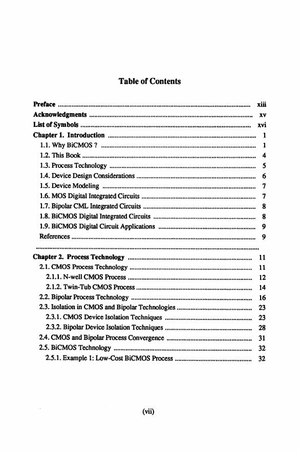
Table of Contents
Preface . ....... .................................. ....................................................................... xiii
Acknowledgments ................................................................................................ xv List of Symbols .................................................................................................... xvi
Chapter 1. Introduction ................ .............. ......................................... ................ 1
1.1. Why BiCMOS? ........................................................................................... 1
1.2. This Book.. ............ ................. ......... ....... ............ ................. ............ ..... ......... 4 1.3. Process Technology ...................................................................................... 5
1.4. Device Design Considerations ...................................................................... 6 1.5. Device Modeling .......................................................................................... 7
1.6. MOS Digital Integrated Circuits .......... ................................................ ......... 7 1.7. Bipolar CML Integrated Circuits .. ........................ ................................. ....... 8 1.8. BiCMOS Digital Integrated Circuits ............................................................ 8 1.9. BiCMOS Digital Circuit Applications ......................................................... 9
References ................. .................... ............ ..................... ............................. ......... 9
Chapter 2. Process Technology......................................................................... 11
2.1. CMOS Process Technology........................................................................ 11 2.1.1. N-well CMOS Process ......................................................................... 12 2.1.2. Twin-Tub CMOS Process .................................................................... 14
2.2. Bipolar Process Technology....................................................................... 16 2.3. Isolation in CMOS and Bipolar Technologies ............................................ 23
2.3.1. CMOS Device Isolation Techniques ................................................... 23 2.3.2. Bipolar Device Isolation Techniques ................................................... 28
2.4. CMOS and Bipolar Process Convergence .................................................. 31 2.5. BiCMOS Technology ................................................................................. 32
2.5.1. Example 1: Low-Cost BiCMOS Process ............................................. 32
(vii)
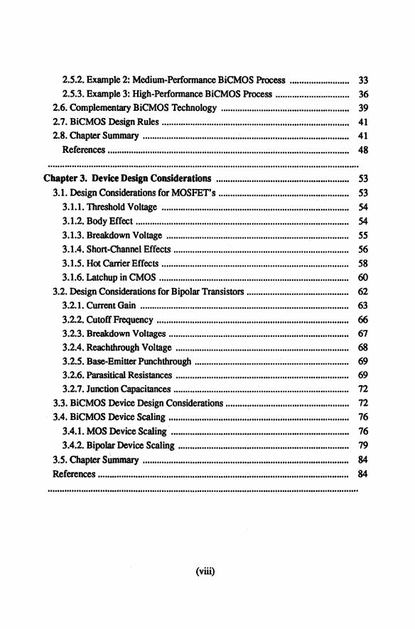
2.5.2. Example 2: Medium-Performance BiCMOS Process ......................... 33 2.5.3. Example 3: High-Performance BiCMOS Process ............................... 36
2.6. Complementary BiCMOS Technology...................................................... 39 2.7. BiCMOS Design Rules ............................................................................... 41 2.8. Chapte,r Summary ........................................ ~............................................... 41
References .......................................................................•........•...................•. 48
Chapter 3. Device Desip Considerations ........................................................ 53 3.1. Design Considerations for MOSFET's ....................................................... 53
3.1.1. Threshold Voltage ............................................................................... 54 3.1.2. Body Effect .......................................................................................... 54
3.1.3. Breakdown Voltage ...................................... , ..................... ~................ S5 3.1.4. Short-Channel Effects ....................... ~.................................................. 56 3.1.5. Hot Carrier Effects ............................................................................... 58
3.1.6. utchup in CMOS ................................................................................ 60 3.2. Design Considerations for Bipolar Transistors ........................................... 62
3.2.1. Current Gain •...••....•.•.••••...•••••••••.•.•••.•.•.••••.•••••..•.•.••••••••••••••••••.••..•••••••• 63
3.2.2. Cutoff' Freq,uency ................................................................................. 66 3.2.3. Breakdown Voltages ............................................................................ 67 3.2.4. Reachthrough Voltage ......................................................................... 68 3.2.5. Base:-Bmiuer Punchthrough ................................................................. 69 3.2.6. Parasitical ResistaJlceS ......................................................................... 69 3.2.7. Junction Capacitances .......................................................................... 72
3.3. BiCMOS Device Design Considerations .................................................... 72 3.4. BiCMOS Device Scaling ....................................................................... ~.... 76
3.4.1. MOS I>evice Scaling' ........................................................................... 76 3.4.2. Bipc>lar Device Scaling ........................................................................ 79
3.S. Chapter sUmmary .......................................................•..........•.........•....•..... 84-Refel'ences .......................................................................................................... 84
(viii)
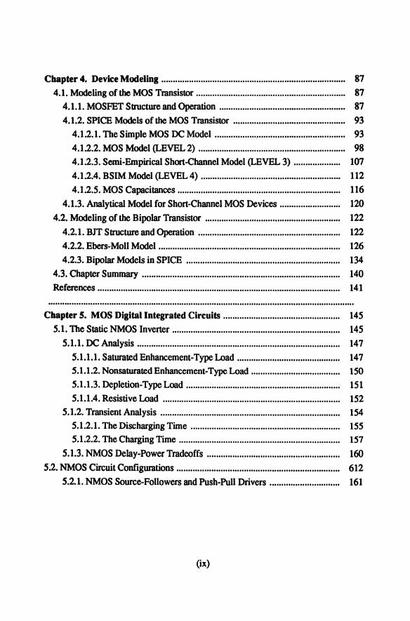
Chapter 4. Device Modeling ............................................................................... 87 4.1. Modeling of the MOS Transistor ................................................................ 87
4.1.1. MOSFET Structure and Operation ...................................................... 87 4.1.2. SPICE Models of the MOS Transistor ................................................ 93
4.1.2.1. The Simple MOS DC Model......................................................... 93 4.1.2.2. MOS Model (LEVEL 2) ............................................................... 98 4.1.2.3. Semi-Empirical Short-Channel Model (LEVEL 3) .................... 107 4.1.2.4. BSIM Model (LEVEL 4) ............................................................ 112 4.1.2.5. MOS Capacitances ...................................................................... 116
4.1.3. Analytical Model for Short-Channel MOS Devices .......................... 120 4.2. Modeling of the Bipolar Transistor .......................................................... 122
4.2.1. BIT Structure and Operation ............................................................. 122 4.2.2. Ebers-Moll Model .............................................................................. 126 4.2.3. Bipolar Models in SPICE .................................................................. 134
4.3. Chapter Summary ..................................................................................... 140 References ...................................................................... .................................. 141
Chapter S. MOS Digital Integrated Circuits .................................................. 145 5.1. The Static NMOS Inverter ........................................................................ 145
5.1.1. DC Analysis ....................................................................................... 147 5.1.1.1. Saturated Enhancement-Type Load ............................................ 147 5.1.1.2. Nonsaturated Enhancement-Type Load ...................................... 150 5.1.1.3. Depletion-Type Load .................................................................. 151 5.1.1.4. Resistive Load ............................................................................ 152
5.1.2. Transient Analysis ............................................................................. 154 5.1.2.1. The Discharging Time ................................................................ 155 5.1.2.2. The Charging Time ..................................................................... 157
5.1.3. NMOS Delay-Power Tradeoffs ......................................................... 160 5.2. NMOS Circuit Configurations ...................................................................... 612
S.2.1. NMOS Source-Followers and Push-Pull Drivers .............................. 161
(ix)
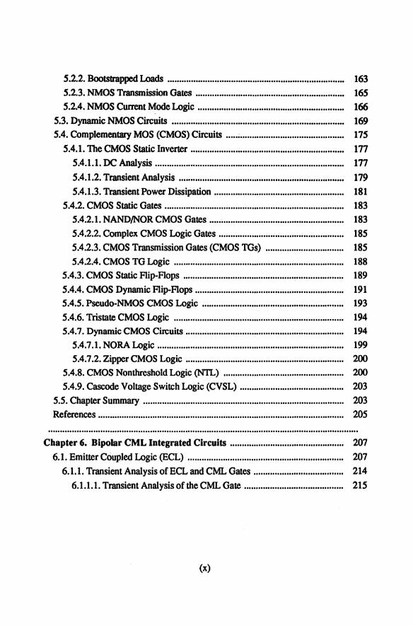
5.2.2. Bootstrap)JCd. I..oads .......................................................................... . 5.2.3. NMOS Transmission Gates ............................................................. .. 5.24. NMOS Current Mode Logic ............................................................. .
5.3. Dynamic NMOS Cireuits ........................................................................ . 5.4. Complementary MOS (CMOS) Circuits •••.. ; .......................................... ..
5.4.1. The CMOS Static Inverter ................................................................ . 5.4.1.1. DC Analysis ............................................................................... .
5.4.1.2. Tl'8IlSient Analysis ..................................................................... . 5.4.1.3. Tl'8IlSient Power Dissipation ...................................................... .
S.4.2. CMOS Static Gates ........................................................................... . 5.4.2.1. NANDIN'OR CMOS Gates ...................................................... ... 5.4.2.2. Complex CMOS Logic Gates ................................................... .. 5.4.2.3. CMOS Transmission Gates (CMOS TGs) ............................... .. 5.4.2.4. CMOS TG Logic ....................................................................... .
5.4.3. CMOS Static Flip-Flops ................................................................... . 5.4.4. CMOS Dynamic Flip-Flops .............................................................. . 5.4.S. Pseudo-NMOS CMOS Logic ........................................................... . 5.4.6. Trista.te CMOS I..ogic .....•...••••••••...•.....••••..•.••..•.•...•..•••..•••.•..•.••...•....• 5.4.7. Dynamic CMOS Circuits ................................................................. ..
5.4.7.1. NORAwgic •••............•..................•..•.....•••••••••..••••••..••.••••••••..•••• 5.4.7.2. Zipper CMOS Logic .................................................................. .
5.4.8. CMOS Nonthreshold Logic (NTL) .................................................. .
5.4.9. Cascade Voltage Switch Logic (CVSL) .......................................... .. S.S. Chapter Summary .................................................................................... . References ....................................................................................................... .
Chapter 6. Bipolar CML Integrated Circuits ............................................... .
6.1. Emitter Coupled Logic (ECL) ................................................................. . 6.1.1. Transient Analysis of ECL and CML Gates .................................... ..
6.1.1.1. Transient Analysis of the CML Gate ....................................... ...
(x)
163 165 166 169 175 171
177 179 181
183 183 185 185 188
189 191 193 194 194 199 200 200 203 203 205
207 207 214
215
6.1.1.2. Transient Analysis of the ECL Gate ........................................... 221 6.1.2. ECL Current Sources ......................................................................... 224 6.1.3. ECL Reference Voltages ................................................................. ~. 226
6.2. Emitter Function Logic (EFL) .................................................................. 227 6.2.1. EFL Cell Implementation .................................................................. 232 6.2.2. EFL Logic Building Blocks: Combinatorial Logic Elements ........... 234 6.2.3. EFL Logic Building Blocks: Sequential Logic Elements .................. 240
6.3. OC Specifications for a Practical EFL ...................................................... 247 6.4. Chapter Summary ..................................................................................... 249 References ........................................................................................................ 249
Chapter 7. BiCMOS Digital Integrated Circuits ........................................... 251 7.1. Comparison between Bipolar and MOS Transistors ................................ 251 7.2. BiCMOS Totem-Pole Inverter .................................................................. 255
7.2.1. DC Characteristics of the BiCMOS Inverter ..................................... 259 7.2.2. Transient Analysis of the Totem-pole BiCMOS Inverter .................. 265 7.2.3. Delay Dependence on the Device Parameters ................................... 278 7.2.4. BiCMOS Circuit Design .................................................................... 278 7.2.5. Comparing CMOS and BiCMOS Inverters' Speed ........................... 283 7.2.6. Layout of the BiCMOS Inverter ........................................................ 287 7.2.7. BiCMOS Gates .................................................................................. 289
7.3. Full-Voltage-Swing BiCMOS Drivers ..................................................... 290 7.3.1. The AC Effects on the Swing of the Conventional BiCMOS Gate... 290 7.3.2. BiNMOS- Circuits .............................................................................. 294 7.3.3. Full-Swing BiCMOS Circuits with Shunting Techniques ................ 295 7.3.4. Full-Swing Common-Follower Complementary BiCMOS Circuits. 300 7.3.5. Full-Swing Common-Emitter Complementary BiCMOS Circuits... 303 7.3.6. CMOS versus BiCMOS under Supply Voltage Scaling ................... 310
7.4. Current Mode BiCMOS Circuits .............................................................. 313 7.4.1. The Basic MOS/Bipolar Merged CMS Cell ...................................... 315
(xi)
7.4.2. MOS/Bipolar Merged CML Gates .................................................... 317 7.4.3. Multi-Emitter MOS/Bipolar Merged CML Gates ............................. 321
7.5. Chapter Summary ..................................................................................... 323 References ........................................................................................................ 325
Chapter 8. BiCMOS Digital Circuit Applications ......................................... 329 8.1. Adders ....................................................................................................... 329
8.1.1. Combinational Full-Adder ................................................................. 329 8.1.2. Carry Lookahead Adder ..................................................................... 332 8.1.3. Carry Propagation Adder ................................................................... 341
8.2. Multiplier .......................... ..... ......... ........................... ............................ ... 346 8.3. Random Access Memory .......................................................................... 348
8.3.1. Read Only Memory ........................................................................... 348 8.3.2. Static RAM ........................................................................................ 353 8.3.3. Dynamic RAM ................................................................................... 366 8.3.4. Content Addressable Memory ........................................................... 367
8.4. Programmable Logic Arrays ..................................................................... 371 8.5. Data Path ................................................................................................... 376
8.5.1. Arithmetic Logic Unit ........................................................................ 376 8.5.2. Shifter ................................................................................................ 377 8.5.3. Register File ....................................................................................... 378
8.6. BiCMOS Logic Cells ................................................................................ 380 8.7. BiCMOS Gate Arrays ............................................................................... 381 8.8. Chapter Summary ..................................................................................... 389 References ...................... ....... .......... ........................ ..... ................. ................... 390
Index .................................................................................................................... 395
(xii)
Preface BiCMOS has faced, as any emerging technology, fierce opposition, but nevertheless has been widely accepted. The need for BiCMOS has been and still is a controversial issue. The cost of high-performance BiCMOS process speaks against it. However, there are other arguments supporting the need for such a technology. The comparison between the cost of CMOS and BiCMOS is not trivial especially if we account for the increasing expenses· of scaling CMOS. In other words, adding bipolar to an existing CMOS process might be cheaper than scaling CMOS to obtain the same performance improvemenL On the other hand, the high cost of BiCMOS may be justified by the high performance it can offer. In general, the application itself will dictate the technology that is to be used. If CMOS alone can satisfy the requirements, then it is more cost effective to use CMOS. Yet there are applications where the requirements can be only satisfied by using BiCMOS. There are currently commercial BiCMOS digital products such as high-speed SRAMs, fast microprocessors, gate arrays, in addition to digital, analog and mixed signal BiCMOS ASICs.
The technology for BiCMOS fabrication has matured over the last decade, yet the development of circuits and systems for such a technology is still lagging. There is a great interest among digitaVanalog circuit and system designers to develop techniques to exploit the flexibility that BiCMOS offers.
A large number of reports and technical papers have been published on the development of BiCMOS processes, circuits and systems. This book is an attempt to introduce many of the published ideas and concepts in order to assist students, researchers and design engineers to review the progress achieved so far. For example, in Chapter 2, we introduce the main BiCMOS processes and their performance/cost tradeoffs. In Chapter 7, we present the basic digital BiCMOS structures. The advantages of such circuits over CMOS are explained as well as their limitations. The application of BiCMOS for digital circuits and systems is illustrated in Chapter 8. Moreover, we have added two overview chapters; Chapter 5 on MOS IC's and Chapter 6 on bipolar current mode logic circuits. These two chapters were added because it is expected that future BiCMOS systems will not be limited to the use of BiCMOS circuit structures. The synergy of different structures and logic families will allow for better management of the overall speed and power. Therefore, we believe that those who work in this field should be familiar with the fundamentals of MOS and bipolar CML as well.
This book is also intended for senior undergraduate and graduate Electrical and Computer Engineering students who are interested in digital circuit design. Exposing the students at an early stage to the different technologies and design styles
(xiii)
is of great benefit to them. To those students we have also included Chapters 3 and 4, which introduce important basic infonnation regarding the sttuctures, operation and modeling of MOS and bipolar ttansistors. Such basic knowledge is essential for circuit designers because of the close interaction between device characteristics and circuit perfonnance. This book is an early contribution to the field of digital BiCMOS circuit design. It contains a collection of the contributions of all those who have devoted their time and effort to help us learn more about this field. We do not claim that this text is complete. In many instances, we have tried to summarize the work of others. So those who have special interest in one of the topics have to refer to the given references. There is still the need for more research, investigation and experimentation to fmd answers to many of the unanswered questions regarding the optimum use of BiCMOS circuit structures. We are sure that the relentless search for better perfonnance and quality will continue and will result in interesting and innovative ideas. We hope that the readers of this book will find it useful and that it will add to their knowledge and assist them in contributing to the state-of-the-art of BiCMOS digital circuit design.
(xiv)
S.H.K. Embabi A. Bellaouar M.I. Elmasry
Acknowledgements We would like, first of all, to acknowledge the countless blessings of God Almighty throughout our tifes. We would also like to thank our families whose support and endurance helped us to complete writing this book.
Writing this book would have been impossible without the knowledge contributed by the researchers and workers in this area. Their effort is deeply appreciated. We also extend our thanks to Mr. Carl Harris from Kluwer Academic Publishers for encouraging us to work on this project.
We would also like to thank the reviewers for their careful and thorough review as well as their valuable comments and suggestions which resulted in some improvements. Special thanks to Drs. S. Rofail and Ali Salama for their critical review of the manuscript and fruitful discussions. Our gratitude goes to all our colleagues in the Department of Electrical and Computer Engineering at the University of Waterloo for their support and encouragement, in particular, M. Elrabaa, W. AI-Mulla and P. Harvey.
The research work of the authors reported in this book has been supported in part by NSERC, BNR, NTE, ITRC and MICRONET. This support is greatly appreciated. One of the authors, S.H.K. Embabi, would like to thank his colleagues in the Department of Electrical Engineering at Texas A&M University for their support, in particular, Professor E. Sanchez-Sinencio and Professor J.W. Howze. We appreciate the effort of those who assisted us in various ways to prepare the manuscript and the figures, in particular, J. Pache, D. Pu, A. Dajani, P. Regier and T. Creasy.
(xv)
AE Ac PI (orp,,)
P BVDS
BVCBO
BVCEO
Ct:
C. C. C. Cd
C"" CL
CD C"
DIIIJ
DpE
DJ
Eo f.
Ir Y YE IDS
I DS6111
IB Ic
List of Symbols
emitter area
collector area
maximum forward current gain.
forward current gain as function of the collector cmrenL drain-source breakdown voltage.
collector-base breakdown voltage.
collector-emitter breakdown voltage.
base-collector capacitance.
base-emitter capacitance.
collector-substrate capacitance.
Gate capacitance.
source (drain) depletion capacitance.
gate to source (drain) overlap capacitance.
external load capacitance. diffusion capacitance. total output capacitance.
diffusion constant for the electrons in the base. diffusion constant for the holes in the emitter.
implantation dose to adjust the threshold voltage.
permittivity of oxide.
permittivity of silicon.
cutoff frequency.
body effect coefficient. emitter injection efficiency.
drain-soUlCe cmrenL
drain-source saturation cmrent.
basecmrenL
collector cmrent.
(xvi)
IE emitter current.
I K forward knee current.
IHu high level injection current
I. transport saturation current
I.. eML current
ITF 'tlo high-current parameter.
h forward knee current density.
k Boltzman constant. KN NMOS saturation current factor
Kp PMOS saturation current factor
L drawn channel length. L.JJ effective channel length.
A channel length modulation factor. N. channel doping concentration at the surface.
N 1M . channel doping concentration below the surface.
N B base doping concentration.
Nc collector doping concentration.
NE emitter doping concentration.
N.pi epitaxial layer doping concentration.
N G acceptor doping concentration.
Nd donor doping concentration.
Mj junction exponent (grading factor) .
• j junction built-in potential.
•• surface potential of silicon.
..... gate electrode and silicon work function difference.
RB base resistance.
RBe extrinsic base resistance.
RBi intrinsic base resistance.
Rc collector resistance.
RE emitter resistance.
(xvii)
T temperature.
1./0 minimum forward transit time.
1./ forward transit time.
to% gate oxide thickness.
S subthreshold swing. VAF forward early voltage
VAR reverse early voltage
VB MOS bulk (substrate) voltage.
VBC base-collector voltage.
VBE base-emitter voltage.
VBEoli tum ON base-emitter voltage.
VCE collector-emitter voltage.
VCE.rat saturation collector-emitter voltage.
VFB flat band voltage.
VGS gate-source voltage.
VDS drain-source voltage.
VDSsat saturation drain-source voltage.
V"" power supply voltage.
ViII input voltage.
Vo output voltage.
Vpt punchthrough voltage.
V,t reachthrough voltage.
V .. Voltage swing.
Vt thermal voltage.
VTF 1./ VBC dependence coefficient.
Vr MOS threshold voltage.
Vro MOS threshold voltage when VB=O.
VrN NMOS threshold voltage.
Vrp PMOS threshold voltage.
v .. .., carrier saturation velocity.
(xviii)
W..,. effective channel width.
W D depletion layer width in the bulk of the MOSFET.
WN NMOSFET device width.
Wp PMOSFET device width.
W B emitter width.
WB base width.
We collector width.
XTF 'tf dependence coefficient.
x) source/drain junction depth.
xjB emitter junction depth.
(xix)
DIGITAL BiCMOS INTEGRATED CIRCUIT DESIGN