Embed Size (px)
Citation preview

1
1
Digital Circuits II
Review
Chapter 4 Programmable Logic Devices:
CPLDs and FPGAs with VHDL DesignReferences (Text Book):
1) Digital Electronics, 9th editon, by William Kleitz, published by Pearson
Spring 2015
Paul I-Hai Lin, Professor of ECET
Dept. of Computer, Electrical and Information Technology
Indiana University-Purdue University Fort Wayne
Prof. Paul Lin
2
Topics of Discussion
PLD (Programmable Logic Devices)
Computer-aided design (CAD) tools
VHDL - VHSIC Hardware Description Language
• VHSIC - Very High Speed Integrated Circuit
PLD Design Process
Altera Quartus II
Examples: Combinational Logics Designs
Prof. Paul Lin

2
3
PLD (Programmable Logic Devices) and CAD
Design Tools
PLD
• Contains thousands of basic logic gates in a single package
• Capable of performing advanced sequential functions
• Must be configured to perform a specific function
Figure 4.1 Sample PLDs: (a) Altera MAX CPLD; (b) Altera Cyclone
FPGA.
Prof. Paul Lin
4
PLD (Programmable Logic Devices) and CAD
Design Tools
PLD
Computer-aided design (CAD) is used to draw the
schematic.
Schematic Capture converts to a binary file.
• Program uses the file to alter PLD internal connections,
implementing the desired function.
VHDL - VHSIC Hardware Description Language
• VHSIC - Very High Speed Integrated Circuit
Prof. Paul Lin

3
5
Six Steps in the PLD Design Flow
1. Define the problem
2. Develop the equations
3. Enter the design
4. Simulate the input/output
conditions
5. Program the PLD
6. Test the final programmed PLD
Prof. Paul Lin
6
PLD Design Flow Example
Implementing the equation X = A’B + (B+C)’ using
7400—series logic ICs
Prof. Paul Lin

4
7
PLD Design Flow Example
Implementing the equation X = A’B + (B+C)’ using a
PLD: Altera MAX EPM7128S
Prof. Paul Lin
8
PLD Architecture
SPLD (Simple Programmable Logic Device)• Four basic types: SPLDs, CPLDs, FPGAs, and
ASICs
• Most basic and least expensive
• Configurable logic gates
• Programmable interconnection points
• Memory flip-flops
• Typically 16 inputs plus complements and10 outputs
• AND gate outputs called product terms
Prof. Paul Lin

5
9
PLD Architecture
PAL (Programmable Array Logic)
• Gives sum-of-products form
• Uses fixed-input OR gates
PLA (Programmable Logic Array)
• Gives sum-of-products form
• Uses programmable-input OR gates
Flip-flop memory section
Data steering circuitry
Prof. Paul Lin
10
PLD Architecture
PAL16L8
• The number 16 means 16 inputs
• The number 8 means 8 outputs
• The letter L means outputs are active LOW
Prof. Paul Lin

6
11
PLD Architecture
CPLD (Complex Programmable Logic Device)
• Combines several PAL-type SPLDs into a single
package
• Nonvolatile – memory is not lost when power is
removed
• Can be repeatedly programmed to implement
different functions
Prof. Paul Lin
12
PLD Architecture
FPGA (Field-Programmable Gate Array)
• Uses a look-up table (LUT) – a truth table listing
all possible input/output combinations.
• More dense and faster than CPLDs
• Volatile – programming is lost when power is
removed.
Must be reprogrammed each time power is
applied
• The Altera Cyclone series is a good example
Prof. Paul Lin

7
13
PLD Architecture
ASIC stands for application-specific
integrated circuit.
• Used for large quantity demand
• After testing on FPGA design is transferred to
ASIC.
• Nonvolatile so programming not lost when power
is removed.
• Can be pin compatible with FPGA
Prof. Paul Lin
14
Using PLD to Solve Basic Logic Designs
Schematic editor
• Connect pre-defined logic symbols
VHDL editor
• Define the logic
Compiler
• Language and symbol translation program
Waveform simulator
• To check the logic operation
Prof. Paul Lin
8
15
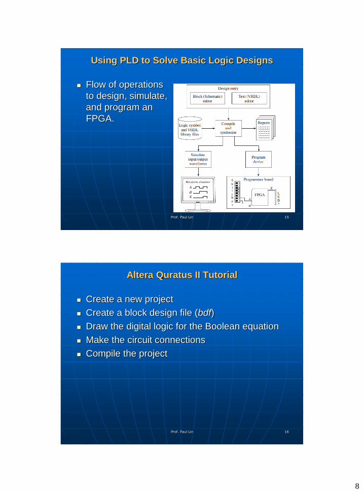
Using PLD to Solve Basic Logic Designs
Flow of operations
to design, simulate,
and program an
FPGA.
Prof. Paul Lin
16
Altera Quratus II Tutorial
Create a new project
Create a block design file (bdf)
Draw the digital logic for the Boolean equation
Make the circuit connections
Compile the project
Prof. Paul Lin

9
17
Altera Quratus II Tutorial
Create a vector waveform file (vwf)
Add inputs and outputs to the waveform display
Create timing waveforms for the inputs
Perform a functional simulation of the x-output
Prof. Paul Lin
18
Altera Quratus II Tutorial
Use the Altera development and education
board to program an FPGA.
• Assign pins
• Recompile the project
• Program the FPGA
• Test the logic
Use the VHDL text editor to recreate the design
used in the block design.
Prof. Paul Lin

10
19
Design Example
Figure 4-13: Two-Input NAND Gate
Prof. Paul Lin
20
Example 4-1 (e): X = A + (BC’); Y = AB + (B+C)’
Prof. Paul Lin

11
21
Example 4-1 (e): X = A + (BC’); Y = AB + (B+C)’
Prof. Paul Lin
22
Example 4-2: X = AB’ + A’B
Prof. Paul Lin
12
23
Example 4-2: X = AB’ + A’B
Prof. Paul Lin
24
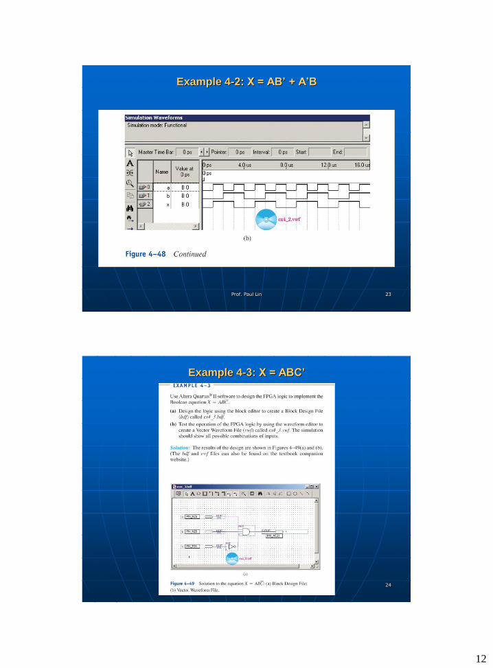
Example 4-3: X = ABC’
Prof. Paul Lin

13
25
Example 4-3: X = ABC’
Prof. Paul Lin
26
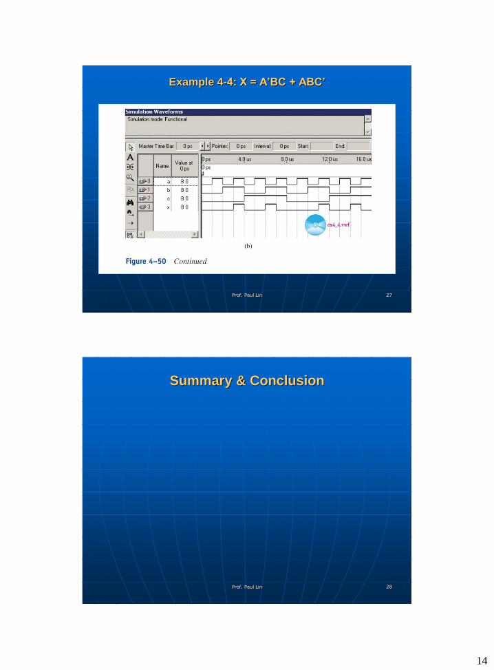
Example 4-4: X = A’BC + ABC’
Prof. Paul Lin
14
27
Example 4-4: X = A’BC + ABC’
Prof. Paul Lin
Summary & Conclusion
Prof. Paul Lin 28