Embed Size (px)
DESCRIPTION
Digital Cochlea Model Implementation Using Xilinx XC3S500E Spartan-3E FPGA. Isabel Gambin, Ivan Grech, Owen Casha, Edward Gatt and Joseph Micallef Department of Microelectronics and Nanoelectronics University of Malta. Overview. Biological Cochlea Cochlear Model Digital Filter Design - PowerPoint PPT Presentation
Citation preview
Isabel Gambin, Ivan Grech, Owen Casha, Edward Gatt and Joseph Micallef
Department of Microelectronics and NanoelectronicsUniversity of Malta
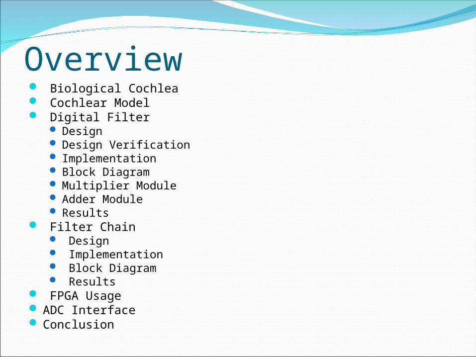
Overview Biological Cochlea Cochlear Model Digital Filter
Design Design Verification Implementation Block Diagram Multiplier Module Adder Module Results
Filter Chain Design Implementation Block Diagram Results
FPGA Usage ADC Interface Conclusion
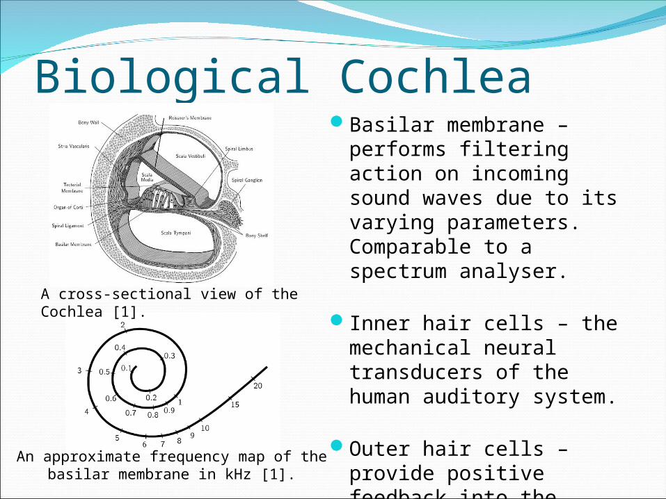
Biological CochleaBasilar membrane –
performs filtering action on incoming sound waves due to its varying parameters. Comparable to a spectrum analyser.
Inner hair cells – the mechanical neural transducers of the human auditory system.
Outer hair cells – provide positive feedback into the membrane to amplify otherwise inaudible sounds. Comparable to an AGC system.
A cross-sectional view of the Cochlea [1].
An approximate frequency map of the basilar membrane in kHz [1].
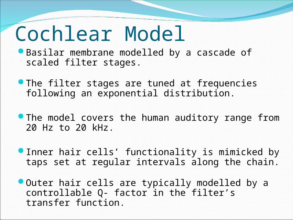
Cochlear ModelBasilar membrane modelled by a cascade of
scaled filter stages.
The filter stages are tuned at frequencies following an exponential distribution.
The model covers the human auditory range from 20 Hz to 20 kHz.
Inner hair cells’ functionality is mimicked by taps set at regular intervals along the chain.
Outer hair cells are typically modelled by a controllable Q- factor in the filter’s transfer function.
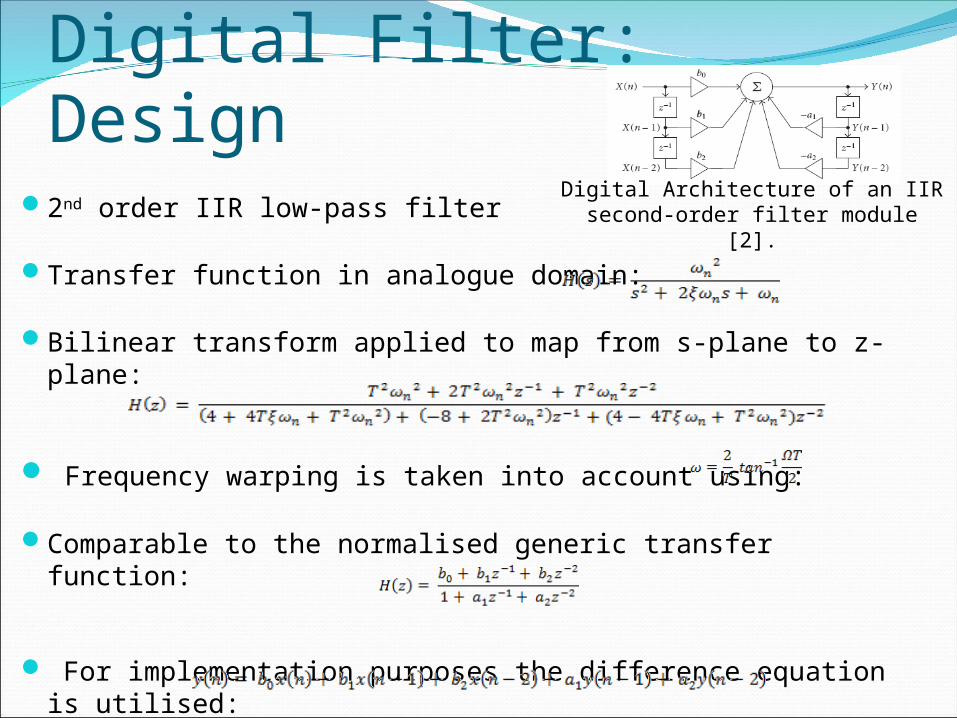
Digital Filter: Design 2nd order IIR low-pass filter
Transfer function in analogue domain:
Bilinear transform applied to map from s-plane to z-plane:
Frequency warping is taken into account using:
Comparable to the normalised generic transfer function:
For implementation purposes the difference equation is utilised:
Digital Architecture of an IIR second-order filter module [2].
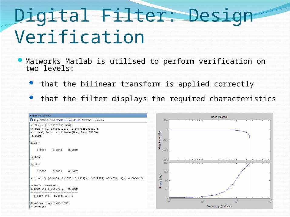
Digital Filter: Design VerificationMatworks Matlab is utilised to perform verification on two
levels:
that the bilinear transform is applied correctly
that the filter displays the required characteristics
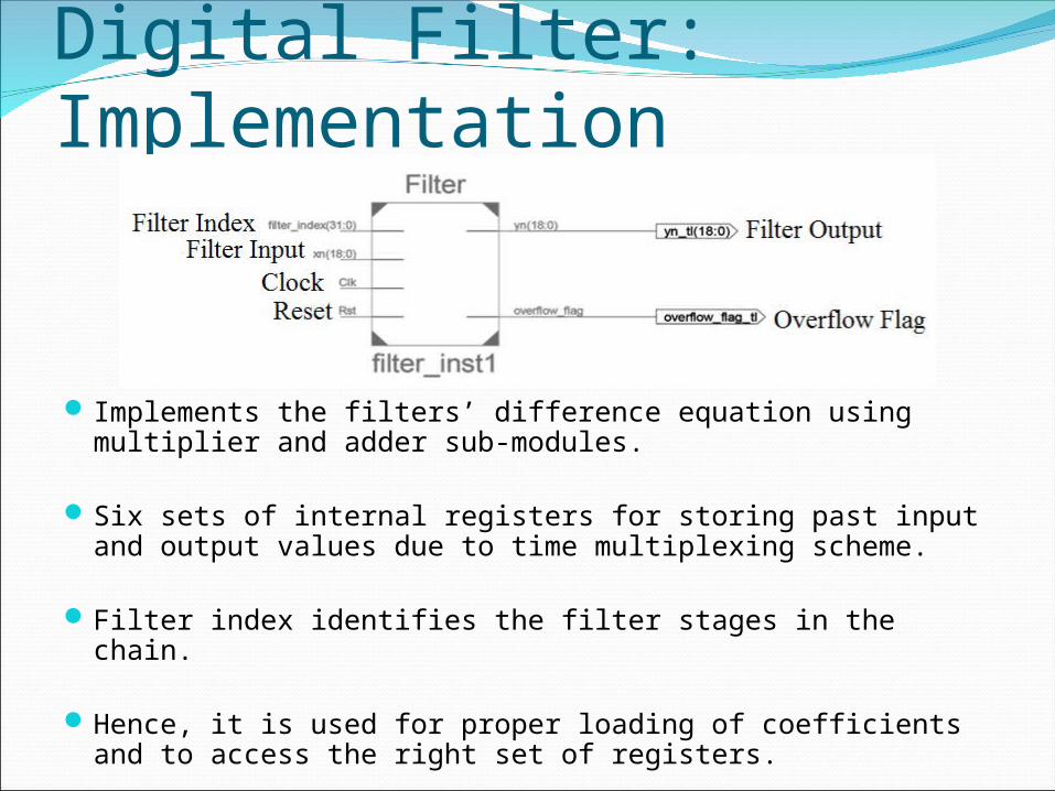
Digital Filter: Implementation
Implements the filters’ difference equation using multiplier and adder sub-modules.
Six sets of internal registers for storing past input and output values due to time multiplexing scheme.
Filter index identifies the filter stages in the chain.
Hence, it is used for proper loading of coefficients and to access the right set of registers.
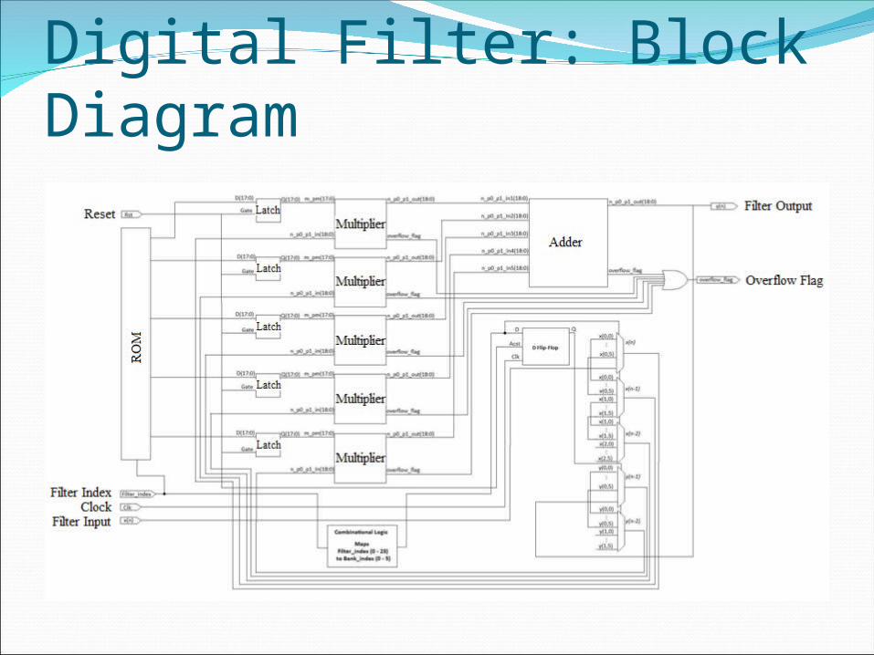
Digital Filter: Block Diagram

DFX Representation UsedUses a single bit exponent to choose between two
fixed point representations, lower Num 0 range and a higher Num 1 range
DFX representation implemented is 19_16_8 (n_p0_p1)n - word lengthp0/p1 - positions of the radix from the LSB for the lower
and higher range respectively.
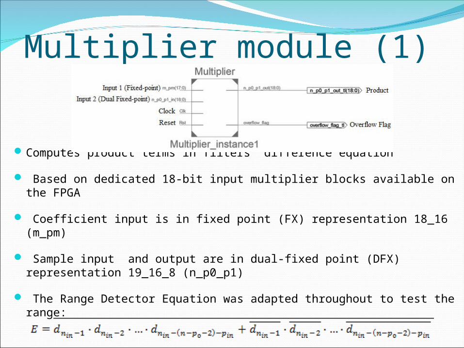
Multiplier module (1)
Computes product terms in filters’ difference equation
Based on dedicated 18-bit input multiplier blocks available on the FPGA
Coefficient input is in fixed point (FX) representation 18_16 (m_pm)
Sample input and output are in dual-fixed point (DFX) representation 19_16_8 (n_p0_p1)
The Range Detector Equation was adapted throughout to test the range:
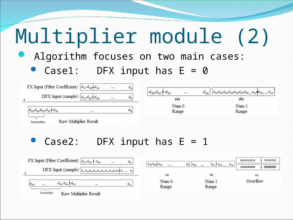
Multiplier module (2) Algorithm focuses on two main cases:
Case1: DFX input has E = 0
Case2: DFX input has E = 1
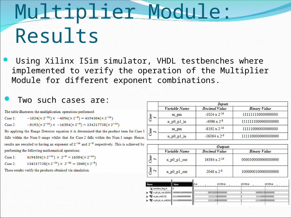
Multiplier Module: Results
Two such cases are:
Using Xilinx ISim simulator, VHDL testbenches where implemented to verify the operation of the Multiplier Module for different exponent combinations.
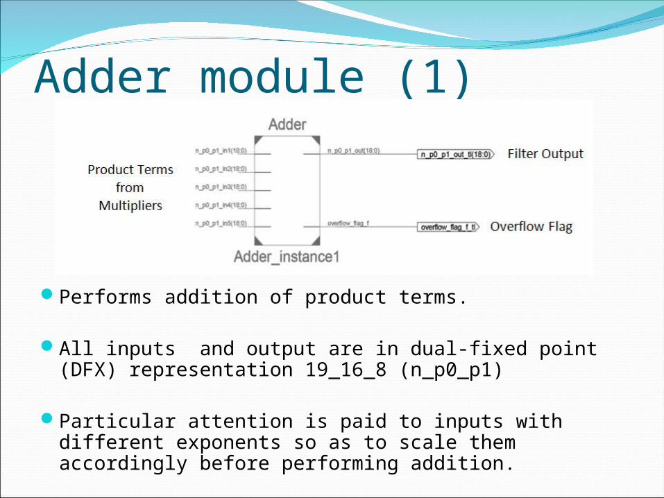
Adder module (1)
Performs addition of product terms.
All inputs and output are in dual-fixed point (DFX) representation 19_16_8 (n_p0_p1)
Particular attention is paid to inputs with different exponents so as to scale them accordingly before performing addition.
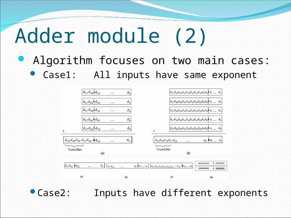
Adder module (2) Algorithm focuses on two main cases:
Case1: All inputs have same exponent
Case2: Inputs have different exponents

Adder Module: Results Using Xilinx ISim simulator, VHDL testbenches are implemented to
verify the operation of the Adder Module for different exponent combinations.
One such case is:
Digital Filter: Results (1)Tests to verify correct functionality of filter module
when all the registers in a particular set are in use.
Tests t0 confirm correct switching between sets of registers to retrieve the past input and output values according to filter stage index.
Input signals, output signals and contents of sub-modules are monitored at each clock cycle during testing.
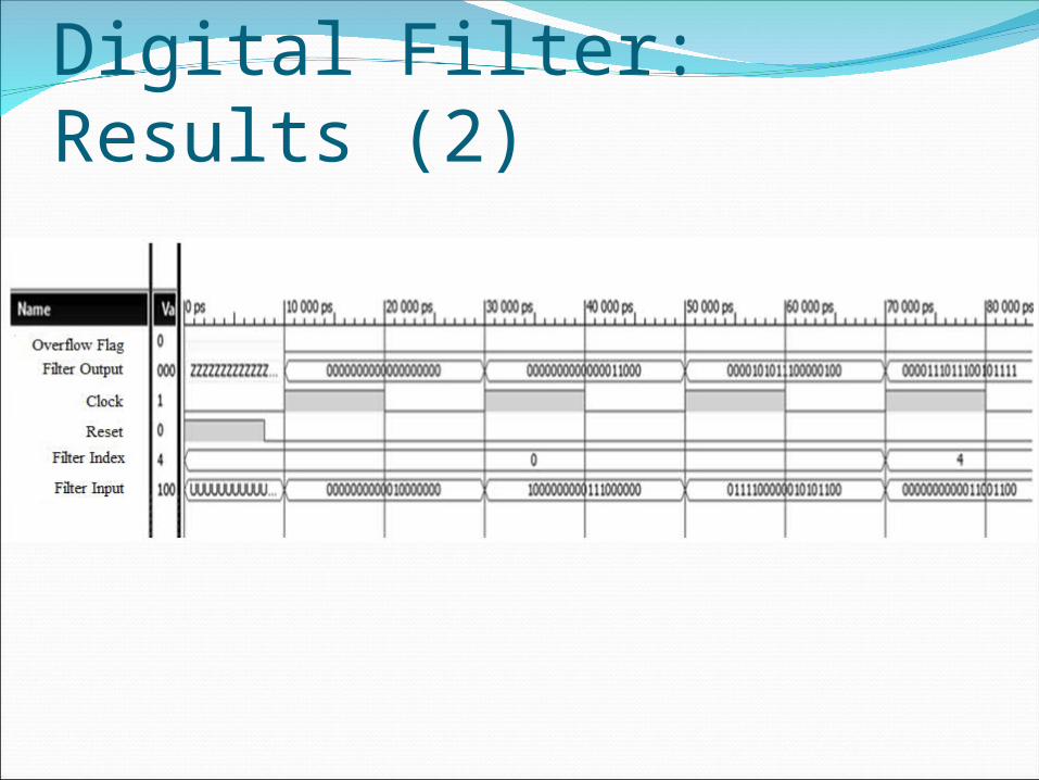
Digital Filter: Results (2)
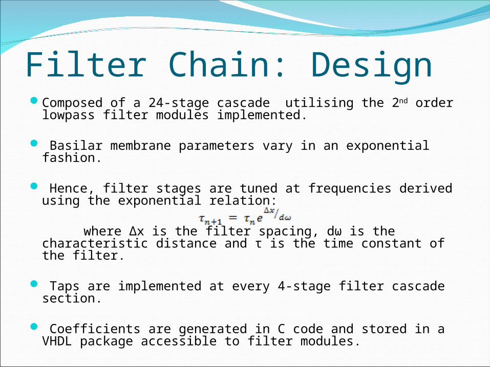
Filter Chain: DesignComposed of a 24-stage cascade utilising the 2nd order
lowpass filter modules implemented.
Basilar membrane parameters vary in an exponential fashion.
Hence, filter stages are tuned at frequencies derived using the exponential relation:
where Δx is the filter spacing, dω is the characteristic distance and τ is the time constant of the filter.
Taps are implemented at every 4-stage filter cascade section.
Coefficients are generated in C code and stored in a VHDL package accessible to filter modules.
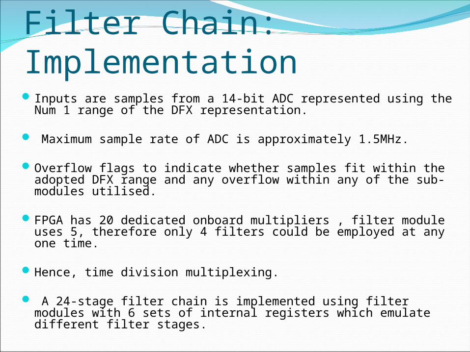
Filter Chain: Implementation Inputs are samples from a 14-bit ADC represented using the
Num 1 range of the DFX representation.
Maximum sample rate of ADC is approximately 1.5MHz.
Overflow flags to indicate whether samples fit within the adopted DFX range and any overflow within any of the sub-modules utilised.
FPGA has 20 dedicated onboard multipliers , filter module uses 5, therefore only 4 filters could be employed at any one time.
Hence, time division multiplexing.
A 24-stage filter chain is implemented using filter modules with 6 sets of internal registers which emulate different filter stages.
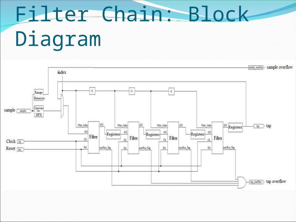
Filter Chain: Block Diagram
Filter Chain: Results (1)
Verified that sample values are represented correctly in DFX format.
Verified correct propagation of samples throughout the filter chain by monitoring intermediate signals and variables.
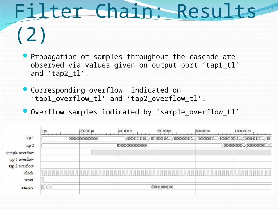
Filter Chain: Results (2) Propagation of samples throughout the cascade are observed
via values given on output port ‘tap1_tl’ and ‘tap2_tl’.
Corresponding overflow indicated on ‘tap1_overflow_tl’ and ‘tap2_overflow_tl’.
Overflow samples indicated by ‘sample_overflow_tl’.
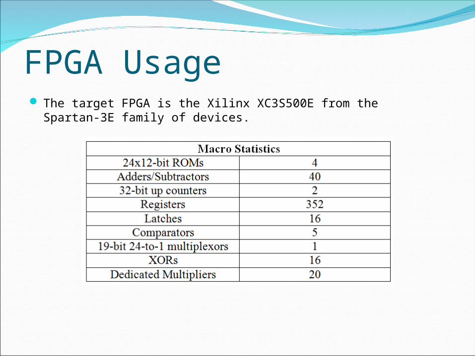
FPGA Usage The target FPGA is the Xilinx XC3S500E from the
Spartan-3E family of devices.
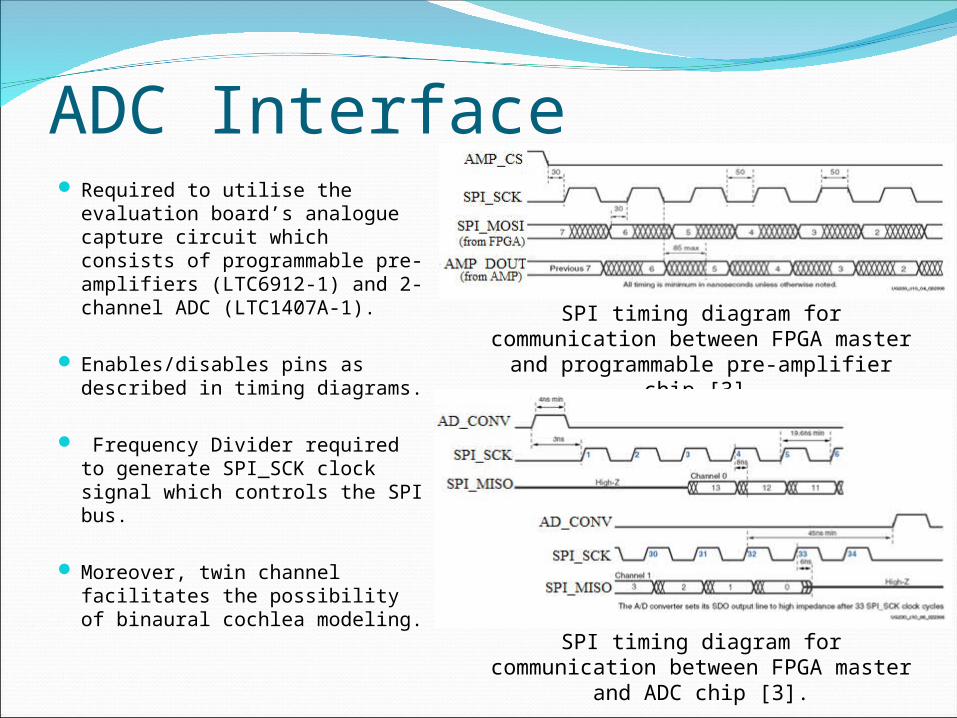
ADC Interface Required to utilise the
evaluation board’s analogue capture circuit which consists of programmable pre-amplifiers (LTC6912-1) and 2-channel ADC (LTC1407A-1).
Enables/disables pins as described in timing diagrams.
Frequency Divider required to generate SPI_SCK clock signal which controls the SPI bus.
Moreover, twin channel facilitates the possibility of binaural cochlea modeling.
SPI timing diagram for communication between FPGA master and
programmable pre-amplifier chip [3].
SPI timing diagram for communication between FPGA master and ADC chip [3].
ConclusionThe qualitative behaviour of the biological cochlea
designed as a cascade of 2nd order IIR lowpass filter modules.
DFX arithmetic allowing the model to operate on a wider range of audio samples without overflow.
In future work, the design could be enhanced by: Modelling to a greater degree of accuracy the nonlinearities
produced by outer hair cells (Automatic Gain Control). Designing a means for outputting data from the cochlear
filter model.Including post-cochlea processing such as pitch detection,
amplitude modulation detection, correlation , speech recognition, monaural and binaural sound localization cues extraction.
References[1]Lloyd Watts, “Cochlear Mechanics: Analysis and
Analog VLSI”, Ph.D. Thesis, California Institute of Technology, 1993
[2]M. P. Leong, Craig T. Jin, Philip H. W. Leong, “An FPGA-Based Electronic Cochlea”, EURASIP Journal on Applied Signal Processing, Vol. 2003, No. 7, pp. 629-638, January 2003
[3]Xilinx. (March 2006), Spartan-3E Starter Kit Board User Guide Version 1.0a, [Online]. Available: http://www.digilentinc.com/Data/Products/S3EBOARD/S3EStarter_ug230.pdf
![Automatic Cochlea Multi-modal Images Segmentation · 2018-04-03 · Automatic Cochlea Multi-modal Images Segmentation Al-Dhamari, CI2018 Methods: Cochlea Model 9 [5] Gerber et al,](https://img.pdfslide.net/doc/110x75/5f8e42f1fe0c2a0180250f2a/automatic-cochlea-multi-modal-images-segmentation-2018-04-03-automatic-cochlea.jpg)