Embed Size (px)
Citation preview
ECE 4850
May 6, 2011
Matthew Fox, Thomas Gilbert, Raysa Suazo
Utah State University, College of Engineering, Electrical and Computer Engineering Department
Digital FM Radio Implementing Stereo Decoding Radio Enforcer

Matthew Fox Paul Gilbert Raysa Suazo [email protected] [email protected] [email protected]
Cell: 435-232-4501 Cell: 801-391-9443 Cell: 435-512-3933 May 6, 2011 Dr. Donald Cripps Department of Electrical and Computer Engineering Utah State University Dr. Cripps,
Enclosed is a copy of our senior design project. We have decided to construct a radio
receiver that can pass the entire FM band and then use frequency-selective tuning in order to
pass the desired channel(s) to a DSP board for the necessary demodulation in order to recover
the transmitted signal. We plan on accomplishing this using a superheterodyne receiver due to
their high frequency selectivity and sensitivity characteristics. We were able to build our own
design based on the frequency plan that we choose to use. Also, we design our own power
circuitry that will feed the radio. As part of the project we achieve stereo sound. For future
design we propose to include multiple-signal demodulation in order to facilitate simultaneous
station recovery. This would allow several stations to be played in different locations without
the need for a separate tuner. This has numerous potential applications in both home and
business settings.
Our team members have all had classes in basic/intermediate electromagnetic theory,
signal processing, digital and wireless communications, and antennas, all of which provide the
base knowledge required for undertaking a project of this scope. We are all available to provide
answers to any questions you may have or provide more information using the supplied contact
information.
Sincerely, Matthew Fox Paul Gilbert Raysa Suazo

Table of Contents
1. Introduction .......................................................................................................................................... 7
2. Review of Conceptual and Preliminary Design ................................................................................... 10
2.1 Problem Analysis ......................................................................................................................... 10
2.1.1 Summary of Specifications .................................................................................................. 10
2.1.2 Summary of Basic Engineering Approach .......................................................................... 12
2.2 Decision analysis ........................................................................................................................ 13
3. Basic Solution Description ................................................................................................................. 15
3.1. Theory ......................................................................................................................................... 15
3.2. Analog Front End ......................................................................................................................... 18
3.2.1. Hardware ............................................................................................................................ 18
3.3 Digital .......................................................................................................................................... 21
3.3.1. Hardware ............................................................................................................................ 22
3.3.2. Software .............................................................................................................................. 22
4. Performance Optimization and System Components ........................................................................ 23
4.1 System Overview ....................................................................................................................... 23
4.2 Analog section ............................................................................................................................. 23
4.2.1. Hardware ............................................................................................................................ 24
4.3. Digital Section ............................................................................................................................. 32
4.4 The Construction or Fabrication ................................................................................................. 34
5. Project Implementation/Operation and Assessment ................................................................... 34
5.1 Testing Results ............................................................................................................................ 35
5.1.1. Low-Noise Amplifier (RAMP-33LN) .................................................................................... 35
5.1.2. Bandpass Filter (SXBP-100) ................................................................................................ 37
5.1.3. Lowpass Filter (SXLP-95) .................................................................................................... 38
5.1.4. Voltage Controlled Oscillator (ZOS-150) ............................................................................ 39
5.1.5. Frequency Mixer (ZX05-1MHW) ......................................................................................... 40
5.1.6. Low-Noise Amplifier (ZFL-1000LN) ..................................................................................... 41
5.1.7. Bandpass Filter (SBP-10.7) ................................................................................................. 41
5.2. Complete RF Front End ............................................................................................................... 41
6. Final Scope of Work Statement .......................................................................................................... 42

6.1. Task to be done ........................................................................................................................... 42
6.2 Lessons Learned .......................................................................................................................... 42
6.3 Suggestions for future works ...................................................................................................... 43
6.4 Project Specifics .......................................................................................................................... 44
8. Cost Estimation ................................................................................................................................... 44
8.1 Other Issues ................................................................................................................................ 45
9. Project Management Summary .......................................................................................................... 46
9.1 Tasks ............................................................................................................................................ 47
9.2 Time Line ..................................................................................................................................... 48
10. Conclusion ...................................................................................................................................... 49
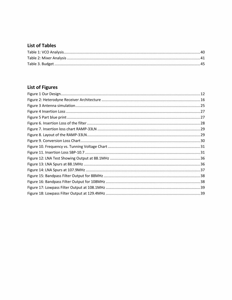
List of Tables Table 1: VCO Analysis .................................................................................................................................. 40 Table 2: Mixer Analysis ............................................................................................................................... 41 Table 3. Budget ........................................................................................................................................... 45
List of Figures Figure 1 Our Design ..................................................................................................................................... 12 Figure 2: Heterodyne Receiver Architecture .............................................................................................. 16 Figure 3 Antenna simulation ....................................................................................................................... 25 Figure 4 Insertion Loss ................................................................................................................................ 27 Figure 5 Part blue print ............................................................................................................................... 27 Figure 6. Insertion Loss of the filter ............................................................................................................ 28 Figure 7. Insertion loss chart RAMP-33LN .................................................................................................. 29 Figure 8. Layout of the RAMP-33LN ............................................................................................................ 29 Figure 9. Conversion Loss Chart .................................................................................................................. 30 Figure 10. Frequency vs. Tunning Voltage Chart ........................................................................................ 31 Figure 11. Insertion Loss SBP-10.7 .............................................................................................................. 31 Figure 12: LNA Test Showing Output at 88.1MHz ...................................................................................... 36 Figure 13: LNA Spurs at 88.1MHz ............................................................................................................... 36 Figure 14: LNA Spurs at 107.9MHz ............................................................................................................. 37 Figure 15: Bandpass Filter Output for 88MHz ............................................................................................ 38 Figure 16: Bandpass Filter Output for 108MHz .......................................................................................... 38 Figure 17: Lowpass Filter Output at 108.1MHz .......................................................................................... 39 Figure 18: Lowpass Filter Output at 129.4MHz .......................................................................................... 39

1. Introduction
Practically everyone has owned and operated an AM/FM radio at some point in their
lives. For the past century, radio has been one of the most effective forms of long-distance
communication due to its flexibility and reliability. In terms of performance, FM radio far
surpasses the sound quality of AM radio, although it makes up for it by requiring at least as
much bandwidth as AM in theory. In practice, however, it is always more. As technology
advances, higher sampling rates for ADC (analog to digital converters) have become available,
making digital radio something that can now easily be achieved.
Digital radio is the process of receiving a signal and processing it digitally as opposed to
the classical analog methods of slope detection, envelope detection, etc. True digital radio
performs all necessary functions for demodulation and downconversion using programmable
DSP (digital signal processing) boards. Since we are taking the ECE department’s Digital Radio
class we must meet the requirement of having an analog front end to receive radio signals and
mix them to a lower IF (intermediate frequency). All of our knowledge for building our receiver
will come from the aforementioned radio receiver class that all members of this project group
are currently taking.
For our project, we will design a front end that can receive the entire FM band (88-
108MHz), downconvert the station of interest to an IF of 10.7MHz, and then process the signal
using the USRP (universal software radio peripheral). The USRP has been provided by Dr.
Gunther and the ECE department for use by anyone taking the radio receiver class. We plan on
being able to tune in any FM station and recover the original stereo audio that was transmitted.

We also hope to be able to recover more than one station at a time, in other words perform
dual-channel recovery.
For our design we decided to go with the tried and true heterodyne architecture due to
a couple inherent advantages to the design which we will discuss later in this report. Our first
order of business was to scour the internet for parts that we could use to build or receiver all
while staying within an allotted budget for the class. All of our components were selected based
upon their ability to meet our frequency plan as well as other important factors such as cost,
size, connector type, and required supply voltage. We managed to find all of our parts through
one online vendor, Mini Circuits, which was very fortunate. Unfortunately, we were informed
by Dr. Gunther to try to reuse any parts that had already been purchased which led to some
design issues that we will touch on later.
After our part selection was complete we had to design the layout of our components as
well as design the supply circuitry to power the components. After much trouble trying to
regulate a computer power supply we decided to go with 9V batteries which turned out to be
more of a hassle that they were probably worth.
Next, we decided to design our own antenna since none of the ones that were available
to us seemed to work very well. This was a fairly simple process that only took a couple hours,
after which we had a functional antenna that could receive FM stations.
Finally, we had to learn to use the USRP and GNU Radio software which allows for easy
interfacing with the USRP using a block diagram approach akin to Simulink. This was sometimes
very frustrating due to our previous lack of exposure to both Linux, which GNU Radio runs on,
and Python, which is the connecting “glue” of the GNU Radio framework.
Overall this has been an enjoyable, if sometimes frustrating project to work on. The
frustration was caused mostly from component failures and other things out of our control,
however. Our final result turned out well. We are able to receive any FM station and can
recover the full stereo recording. Unfortunately, we have been unsuccessful in recovering more
than one station at a time.
In this report we cover our preliminary design and discuss the basic engineering
approach to our design as well as the requirements the design must meet. We then discuss the
basic solution description which contains schematics of all components and initial system
performance estimates.
Next, we touch on our design process and optimization and how we arrived at our final
design choice. This provides a more in-depth look at how our receiver functions on both system
and component levels followed by our testing procedures and our results. We also cover the
scope of our project and what we have accomplished as well as any other issues we have come
across. This will be where we discuss all of the difficulties we have faced over the course of this
project.
Then we have included a cost estimation section which covers the component and man-
hour costs of our project and a project management summary of what has been done and a
Gantt chart of our progress throughout the semester.
Finally, our conclusion restates the purpose of our project and basically summarizes our
final design as well as our costs and timeline. We will also include an appendix that will contain
other useful information such as a bibliography and our part data sheets.

2. Review of Conceptual and Preliminary Design
We want to meet the wants and needs of the consumer by building a portable and
cheap radio. Also we would like to add a few extra things that no other radio can do. In this
section we describe the problem that we addressed and the design analysis of our project.
2.1 Problem Analysis
Nowadays, people want new and exciting devices that can be both cheap and long
lasting. By us exploring and doing some research on different types of radio receiver
architectures, we feel that we can come up with a solution to their demands. Also we would
like to recover two different stations simultaneously and have each station being played at the
same time, one through the right speaker and the other through the left speaker. One other
thing that we are going to do is recover the stereo portion of a Single FM station. So basically
the consumer can either listen to two different stations at the same time or they can choose to
listen to the stereo portion.
2.1.1 Summary of Specifications
A main goal is to implement and test a receiver of our design using the entire FM band.
We need to design a receiver to acquire and demodulate the desired signal(s) as good as we
can. The receiver will be divided into two sections: the RF to IF analog section and the IF to
baseband digital processing section. The analog section is our design of the radio receiver front
end which, consists of specific parts that we need to find that will be inexpensive but still
perform at a high level. The digital section is the part that we use the USRP to demodulate and
recover the FM signals and writing code to perform these tasks using GNU radio.

To address the problem for our consumers to make a cheap and durable radio, we
chose to design our radio receiver front end using the heterodyne architecture for a couple of
reasons:
1. It is one of the most widely used architectures in wireless transceivers. The first
part is where the RF is down-converted to an IF and the second part is where the IF is converted
to baseband. A block diagram of this architecture is shown in figure 2.1.
Figure 2.1 Block diagram of a typical Heterodyne Receiver
2. For the second part where the IF is converted to baseband we are using the
USRP which will do that part for us in software. This was one of the main selling points for us in
this type of architecture, because it minimized the parts that we needed to buy and by doing
that it made the radio receiver front end a lot cheaper. Below in figure 2.2 is a block diagram of
our design.

Figure 1 Our Design
The FM band exists at 88 MHz to 108 MHz so all of the components that we need were
to operate at those frequencies. To limit the image frequency that happens when you down
convert a signal to and intermediate frequency we used two filters a band pass filter and a low
pass filter. By doing this we could practically eliminate the image band which could cause
problems in the down converting process. Since we are using the USRP for the demodulation
sampling at the intermediate frequency will be no problem, because the USRP was built to do
that and also it can perform multiple signal processing at the same time. With the USRP we are
using GNU radio so we can do the real time processing.
First we needed to write out code in Matlab to help us understand how the FM
demodulation works. Second we needed to turn the Matlab code into C code so we could
actually use it in the GNU radio and actually perform the real time processing in our system.
2.1.2 Summary of Basic Engineering Approach
In our radio receiver front end the heterodyne architecture was broken down into
hardware and software. In the hardware side which was the analog part we needed to design a
system that would bring in a radio frequency, a local oscillator frequency, and convert them
into an intermediate frequency. The analog parts consisted of a antenna, amplifiers, filters, a
mixer and a local oscillator. The front ended to be designed to plug into the USRP.
The software side which is the digital part, signal processing was wrote in Matlab so we
could get a more understanding how to write it in C. After we did that we needed to write a
custom block in GNU radio which Dr. Gunther provided us with the steps on how to do that.
Once our custom block was made all we had to do was put our C code in there and GNU radio
did the rest. The final result will be an actual radio front end that you can listen to multiple
stations on the PC or just the stereo part.
The success of this receiver shows that by using the USRP and the heterodyne
architecture that you can limit the amount of analog parts making the cost of a radio less and
use less power to power the analog parts. These benefits provide our consumers with a more
eco friendly environment.
2.2 Decision analysis
The Homedyne and the Low IF architectures are other alternatives to the heterodyne
architecture that we ended up using. We will discuss a little bit about each one and give you
reasons why we went with the heterodyne architecture.
Homodyne receivers translate the channel of interest directly from RF to baseband in a
single stage. For frequency and phase modulated signals, down conversion must provide
quadrature outputs so as to avoid loss of information. The advantages using the Homedyne
architecture:

1. Uses less analog parts
2. No image problem.
3. No mixing down to an IF stage.
4. Power saving because less parts to power.
5. No impedance match required for the LNA because no image reject filter
between LNA and mixer.
Disadvantages using the Homedyne architecture:
1. LO Leakage, this LO leakage mixes with original LO and produces DC offsets in
the mixer output and causes saturation in the rest of the system.
2. DC offset errors; it is the most serious problem in the baseband section of the
homodyne receivers. Since LO frequency is same as carrier frequency, it leaks from receiver to
antenna which interferes with the received frequency band.
3. I/Q miss-match
4. Even order distortion
In Low-IF receiver architecture all the RF signals are translated to a low-IF frequency
which is then down-converted to a base band signal in digital process. Low-IF architecture
comprises the advantages of both heterodyne and homodyne receivers. After filtering and
amplification, all the RF channels are quadrature mixed and down converted to low IF
containing both wanted and unwanted signals. The IF frequency is just one or two channels
bandwidth away from DC, which is just enough to overcome DC offset problems. This was our
second choice.

We chose the heterodyne architecture because it is the most widely used architecture in
wireless communications. By this the parts for the front end will be more widely available. Since
we are using the USRP we will be using fewer parts than the other architectures, because the
USRP does the quadrature mixing for us. Therefore the cost will be less than the other
architectures. Heterodyne architecture has an image reject filter for better channel selection
and has good sensitivity. Basically our project will show that the heterodyne architecture is the
best option for providing customers with what they want and desire in a radio receiver front
end.
3. Basic Solution Description
For our system we decided to implement a heterodyne architecture due to the inherent
advantages of this particular style of FM receiver. This section gives a general overview of the
heterodyne architecture and its implementation.
3.1. Theory
For our design we need to take the entire commercial FM band, which is 20 MHz wide
centered at about 98 MHz and pass it through a frequency mixer that will downconvert the
entire band to allow for signal processing to recover the transmitted information. An
intermediate frequency (IF) of 10.7 MHz was chosen as its popularity in commercial FM receiver

design allows for easier part acquisition and will greatly aid our prototyping process. There are
several different receiver architectures available to us, and we are focusing on a heterodyne
design since its inherent characteristics more closely match intended device usage. This
architecture is shown in figure 1.
Figure 2: Heterodyne Receiver Architecture
The signal to be processed will be collected by an antenna designed for FM frequencies
and sent to a pre-selection filter which will remove all unwanted frequencies outside of the FM
range. This helps remove out-of-band signal energy and partially reject images. The output of
this filter is then fed to a low-noise amplifier in order to boost the signal to a more acceptable
level. Exact gain specifications will be chosen during the actual design and testing phases after
all other parts’ gains/losses have been accounted for. Following that, the amplifier output is
sent through an image rejection (IR) filter which further suppresses the unwanted signals
located at the image frequencies which are determined by the mixer further downstream.
In the next stage, the signal will be passed through a mixer which will perform the initial
downconversion and center the entire FM band at 10.7 MHz. At this point, we can use either a

voltage-controlled oscillator (VCO) or a fixed crystal oscillator for our local oscillator (LO) input
to the mixer depending on whether we want to pass a block of frequencies or tune to a specific
frequency. Since our design purpose is to demodulate any FM station with the hope of
simultaneous recovery, we will need the entire FM block to be mixed, thus leading the use of a
VCO due to its tuning capabilities.
From here, the signal is normally passed through a channel-select filter and then
amplified again before being downconverted to baseband and demodulated through digital
signal processing (DSP) methods. For our application, we most likely will modify the channel-
select filter to act as a smaller block filter if the computer interface cannot process the entire
FM band and/or to perform further image suppression since we want to process multiple
signals. This downconversion will be accomplished through a quadrature method which outputs
the in-phase and quadrature components. Luckily for us the USRP internal FPGA does this for us
using a DDC (digital down converter), so no secondary oscillator or any other hardware
components are needed.
For our DSP purposes, we will be using the aforementioned USRP2010N interfaced to a
computer through GNU Radio software. This allows for a block style program interface akin to
Simulink as well as allowing us to write our own code using C++ to overwrite existing block
functions for any purpose we would deem necessary. The computer hardware will then be used
to output the received signals in real-time as the interface allows for direct output to a sound
card.

3.2. Analog Front End
The analog portion of our design must be able to receive any broadcast FM radio station
and downconvert them to our IF of 10.7MHz. Due to the inherent low power for any received
station, we first amplify the signal being captured by our antenna and then feed it through a
bandpass filter to suppress unwanted frequencies outside the FM band. We then pass the
signal through a lowpass filter in order to suppress image band frequencies. From there, the
signal is passed through a mixer which is fed by a VCO which can tune any FM station to our
chosen IF.
Finally, the signal is amplified again before being sent through one last low pass filter
whose purpose is to remove unwanted signals outside the bandwidth of the desired station. It
has a large enough bandwidth to allow for possible secondary channel recovery, however.
3.2.1. Hardware
All of our analog components were purchased from a single online vendor, Mini Circuits.
We shopped around at a few other vendor sites and decided to go with Mini Circuits due to the
fact that their selection of parts that matched our performance specifications seemed to be
larger than that of their competitors. We were hoping to be able to order all of our components
from one location so this made things much simpler. Our final part selection was made after
extensive evaluation of different oscillator frequencies and their respective characteristics,
image band consideration, gain/loss of each component stage, and cost, as well as ease of use.
We purchased one LNA (low noise amplifier), two bandpass filters, and one lowpass
filter, as well as three test boards for the LNA, lowpass filter, and one bandpass filter since they

were all surface mount components. They had parts that used SMA (coaxial) connectors, but
we liked the specifications of the surface mount parts and don’t mind a little soldering. The test
boards all use SMA connectors as well so no ease of connectivity was lost in our decision. The
VCO, mixer, and secondary amplifier are all parts left over from a previous class since Dr.
Gunther asked us to reuse whatever we could. All of the parts are 50Ω impedance matched so
we don’t have to worry about internal reflections reducing the integrity of our signals. We did
construct our own antenna since we were dissatisfied with the few antennas that were
available in the Anderson Wireless Center. All of these components will be discussed further in
the following paragraphs.
For the antenna we decided to go with a quarter-wavelength monopole design since
they are easy to construct, have an omnidirectional radiation pattern, and have roughly twice
the gain of the same size dipole design as well as a radiation resistance half as large. The
quarter-wavelength was chosen due to it being more manageable as far as portability is
concerned. We soldered on a 50Ω female SMA connector to facilitate easy connection and
removal from our system.
The bandpass filter that we chose for our preselection filter was purchased from Mini
Circuits (PN#SXBP-100). The passband for this filter is from 87-117MHz which goes slightly
above the upper FM range of 108MHz and into the image band for our HSLO (high side local
oscillator) frequencies. This is why we chose a secondary filter to help attenuate our image
band frequencies. The SXBP-100 has a steep roll off; >20dB for frequencies <66MHz and
>143MHz, while for frequencies above and below this range, the attenuation increases sharply
to beyond 40dB. This was a surface mount design that required soldering to a test board also
from Mini Circuits (TB-368) which comes with SMA connectors and has 50Ω impedance.
Our LNA was the RAMP-33LN which we purchased from Mini Circuits along with a test
board to solder it to (TB-10). The test board utilizes SMA connectors and has 50Ω impedance.
This amplifier was chosen due to its overwhelmingly strong performance characteristics as
compared to the other amplifiers we had seen. It has an extremely low noise figure of 1.1dB, a
wide operational bandwidth, a high ITOI (input third-order intercept point), and a relatively
large gain of 22dB for our frequency range. All of this adds up to an amplifier which adds very
little distortion and can amplify relatively strong input signals with little spurious output.
We purchased our secondary or image rejection filter from Mini Circuits (PN#SXLP-95)
as well as a test board (TB-368) for mounting it. This is the same test board used for our pre-
selection filter above. We chose this filter due to the fact that it passes up to 95MHz with very
little loss and its 3dB break point is 108MHz which is the very upper end of the FM band. From
there the attenuation increases sharply to almost 30dB by 146MHz.
The VCO that we chose to use was a leftover part from a previous class also purchased
from Mini Circuits (PN#ZOS-150). This came in an easy to connect package utilizing SMA
connectors and was also 50Ω matched. This coupled with the fact that it would output our LO
frequency range made it an easy substitute for the VCO that we wanted to purchase. It has a
linear tuning range over 75-150MHz and excellent harmonic suppression, typically >23dBc. It
outputs an LO power of +9dBm.
Our mixer was also a pre-used part purchased from Mini Circuits (PN#ZX05-1MHW). It
has an operating range of 0.5-600MHz and uses SMA connectors that are 50Ω impedance. This
mixer has a fairly low conversion loss of 5.8dB as well as good LO-RF and LO-IF isolation; >40dB
in both cases.
Our secondary amplifier was used by a previous class and was also from Mini Circuits
(PN#ZFL-1000LN). It is also a low noise amplifier (2.9dB noise figure) with a large gain, typically
28dB. It is in a casing that uses SMA connectors and is also 50Ω matched. This will further
amplify our incoming signal after it has been selectively filtered and mixed to our IF of 10.7MHz
which will allow for easier signal recovery due to an increased SNR, aided by the fact that both
of our amplifiers have low-noise characteristics.
The final part purchased from Mini Circuits was our channel selection filter (PN#SBP-
10.7). This filter uses SMA connectors and is 50Ω impedance matched the same as all of our
other parts. It was specifically designed for the typical commercial FM radio IF of 10.7MHz
which is why we chose that for our intermediate frequency. This filter had a passband of about
2MHz which will allow for recovery of a tuned station as well as leaving room to try dual-
channel recovery. At >15MHz and <7.5MHz the attenuation is >20dB so this filter also has a
sharp roll off.
3.3 Digital
The digital piece of our radio receiver consists has both hardware and software. The
digital processing takes the incoming signal from our front end and downconverts it to
baseband using a digital downconverter and outputs the data in complex form. Then the signal
is demodulated and output to the sound card of the PC using DSP.
3.3.1. Hardware
The hardware portion of our digital end consists of the USRP connected to a PC for
interfacing and programming. The USRP utilizes a Xilinx Spartan 3A-DSP FPGA and contains a
32-bit RISC microprocessor which is capable of processing signals at rates of up to 100MS/s
(mega-samples per second). There are two onboard digital downconverters that mix, filter, and
decimate incoming signals down to baseband. The USRP is capable of processing signals up to
100MHz wide and can stream signals 50MHz wide through a Gigabit Ethernet connection to a
PC. There are a variety of daughterboards that can be purchased to add to the USRP that
provide flexible, fully integrated front-ends. Basically, the USRP can handle anything we can
throw at it, at least as far as the scope of our project is concerned.
3.3.2. Software
For the software component of our design we first experimented with MATLAB coding
to see how FM demodulation is performed. After that, we moved on to the GNU Radio
software to learn how their block diagrams system programming works and to see how their
pre-made blocks functioned. GNU Radio uses a combination of Python and C++; the operational
code for block internals is written in C while the top level modules are glued together using
Python.
In order to recover stereo sound, we have to first demodulate the incoming FM signal. This
leaves us with a baseband signal about 100 kHz wide, which is the bandwidth of a typical FM

station after it is brought to baseband. Next, the stereo L-R information is AM modulated up to
38 kHz so we must perform AM demodulation on that in order to process the signal for output.
Finally, the monaural L+R information at baseband to about 16 kHz is added to the L-R
information to recover the left channel and subtracted from the L-R information to recover the
right channel. This is how stereo audio decoding is performed in a typical stereo FM receiver.
4. Performance Optimization and System Components
The following section describes the steps that we took to achieve the best optimization to our design.
4.1 System Overview
This section is going to talk about the different analog components that we used and
why we chose them. How GNU radio and the USRP work and why we chose to use them. Also
we will include schematics, the construction, and all of the parts that we used to build the radio
receiver front end.
4.2 Analog section
We had several options of vendors that we could have ordered parts from like: Mini
Circuits, Analog Devices, Maxim, and Texas Instruments just to name a few. We found that Mini
Circuits was the best one for us. They were a little bit more inexpensive than the rest and had
all of the components that we needed to build the front end and were all available. The time it
took to get the parts in was only a week after the order was complete. The components also all
had the same connectors to connect all of the components together. This way we didn’t have
to buy any adaptors and we could use the same thing as all of them.

4.2.1. Hardware
Pretty much all of the components for this project we got was from Mini Circuits, except
for a couple of them which was available to us from Utah State University. Also, Utah State
University provided us with wiring, tools that we used, and various other things that we could
purchase through the ECE store that will be discussed in the construction part. The only thing
that we had to custom make is the antenna since; the one that was available didn’t work up to
our expectations.
4.2.1.1 Antenna Construction
For our antenna there is just one major equation that you need to know and that is the
calculation of λ/4. When using the formula since we are using the entire FM band, you need to
use the center of that band in the equation to determine λ/4. The formula is shown below.
λ4
= 14
cf
Where c is equal to the speed of light which is 3 x 10^8 m/s and f is equal to the
frequency which in this case is the center of the FM band. Since the FM band is at 88 MHz to
108 MHz the centered frequency is at 98 MHz .Shown below is how we used this equation to
determine the length of our antenna.
λ4
= 14∗
3 x 108m/s98 MHz
= 0.765 m
After this calculation we used a free software program that you can easy down load off
of the internet called NEC2. By using this program you can determine the design of your
antenna like what gauge wire will work best and how well it will perform. In our simulation with
wavelength equal to 0.765 m and a frequency of 98 MHz we found that our monopole antenna

worked best with 10 gauge wire and we had a gain of 1.79 dBi. The NEC2 simulation pattern is
shown below in figure.
Figure 3 Antenna simulation
After the simulation and found out what works the best this is how we built the
antenna. First we needed to get the 10 gauge wire which is at length 0.765 m and that converts
to about 30.118 inches and straighten it out. Second we used a half inch PVC cap that we drilled
a hole about the size of the 10 gauge wire so we could put the wire through the hole. This will
act as the base of the antenna so it will stand up straight. Third we drilled another hole into the
side of the pvc cap so we could solder a sma connector to the 10 gauge wire. A picture of the
antenna is shown below.

Figure 4 Antenna
Once the antenna was built we did one more test to it which was connecting it to the
spectrum analyzer. By doing this we could actually see what signals the antenna was receiving
and what the power level was at each signal or station. Below are the results of the spectrum
analyzer.
Figure 5 Antenna Spectrum Results

Band Pass Filter
The basic purpose of this component is to filter out all of the unwanted signals that the
antenna picks up. The pass band of this filter is from 87 MHz to 117 MHz which is in the range
of our FM band. This component (SXBP-100) was bought from Mini Circuits and its case style is
an HF1139. It requires an evaluation board called TB-368 that it needs to be soldered too so we
can used SMA connectors. In figure is the insertion loss, figure is the actual part.
Figure 6 Insertion Loss
Figure 7 Part blue print

4.2.1.2. Low Pass Filter
This filters purpose is mainly to get rid of the unwanted frequencies that previous filter
was unable to get rid of. Since the previous filter went about 11 MHz outside of the FM band.
This filter will reduce the strength of those signals by about half of their signal power so that
the image frequency doesn’t affect any of the signals that we are trying to demodulate and
recover. This component (SXLP-95) was bought from Mini Circuits and it also requires an
evaluation board which is shown above in figure. This filter starts to roll off at 95 MHz and at
108 MHz it is about 3 dB down which is half power. In figure is the insertion loss and figure is
the actual part.
Figure 8. Insertion Loss of the filter
4.2.1.3. Low Noise Amplifier
The purpose of this component is to boost the signal up so it is easier to recover at the
end of the system. Also, to provide as less noise to system as possible that’s why it is a low
noise amplifier. It has a gain of 20 dB, low noise figure of 1.1 dB, and a high IP3 of 30 dBm. This

component (RAMP-33LN) was purchased from mini Circuits and is the last one that requires an
evaluation board (TB-10). In figure is the gain, figure is the actual component.
Figure 9. Insertion loss chart RAMP-33LN
Figure 10. Layout of the RAMP-33LN
4.2.1.4. Mixer
This component is the mixer that takes the RF frequency and the LO frequency and
mixes it down to IF frequency. It also centers the IF frequency at 10.7 MHz. The purpose of this

is so that the frequency is at a lower frequency and it makes it a lot easier to recover the signal
on the Digital side of things. This component was bought from Mini Circuits (ZX05-1MHW) and
is connected by SubMiniature version A (SMA) connectors. In figure is the conversion loss.
Figure 11. Conversion Loss Chart
4.2.1.5. Voltage Controlled Oscillator
This component creates the LO frequency and it depends on what frequency it creates
by the amount of voltage that is fed into it. The range that we need so that we can capture the
entire FM band is from 5 volts to 9 volts. For example if we give it 5 volts it will produce a
frequency that will be fed into the mixer that was stated above and the station 88.1 will be
centered at 10.7 MHz for demodulation. This component was bought from Mini Circuits (ZOS-
150) and is connected by SMA connectors. In figure is the frequency and tuning voltage and
figure is the actual component.

Figure 12. Frequency vs. Tunning Voltage Chart
4.2.1.6. Band Pass Filter no. 2
The main purpose of this filter is basically to filter out the stations that we are not going
to demodulate. So basically it will just pass through a couple of stations and not the entire FM
band. This filter is 2 MHz wide and is centered at 10.7 MHz. This component was bought from
Mini Circuits (SBP-10.7) and is connected with sma connectors. In figure is the insertion loss and
figure is the actual component.
Figure 13. Insertion Loss SBP-10.7
4.3. Digital Section
All of our DSP takes place inside the USRP using GNU Radio as the interface between our
PC and the USRP. The USRP has a DDC (digital down converter) onboard its FPGA that it uses to
reduce any incoming signal to baseband. For our application, 10.7MHz is used as our IF
frequency so in GNU Radio we have set the USRP Source block to have a center frequency of
10.7MHz with a 1MHz bandwidth. In order to pass a signal this wide, we set the source
sampling rate to be 2.205MS/s which is greater than the Nyquist rate and allows for easy
decimation down to the sound card sampling rate of 44.1kHz. This causes the DDC to shift the
10.7MHz IF to baseband, effectively removing the carrier frequency from our received station,
and is then output as complex valued data. The 1MHz bandwidth allows us to process more
than one FM station at a time since each station is allowed 200MHz of bandwidth.
After that, we need to find the instantaneous frequency of the received signal in order
to recover the transmitted information. In order to do this we implement a quadrature
demodulation block that uses complex data for input and outputs floating point data. In order
to compute the instantaneous frequency we followed a few simple steps. First, we computed
the angle between two consecutive samples by multiplying one by the complex conjugate of
the other and then taking the arctangent of the product. In order to recover the instantaneous
frequency, this signal is multiplied by the sample rate which gives the radian frequency, ω
which is then divided by 2π to give the instantaneous frequency. Then, following in the
footsteps of GNU Radio, we divided by the deviation of the FM station to normalize the signal,

which is 75kHz for broadcast FM. This is accomplished by copying a complex in/float out GNU
Radio block and writing our own C++ class for the demodulation operation.
The next piece involves reversing the pre-emphasis added to boost the SNR (signal-to-
noise ratio) of the higher frequencies of an FM broadcast transmission. This is accomplished
through the use of GNU Radio’s De-emphasis block. This block uses a first-order IIR filter in
order to remove the pre-emphasis added to the signal. This leaves us with a 1MHz wide
baseband signal that we must either lowpass filter to recover the single station originally at
10.7MHz, or bandpass filter to recover multiple stations simultaneously. Since our goal is to
recover more than one station at a time, we will have to implement both filtering operations in
order to do so. For an FM station, the monaural information is recorded as L+R and is from
roughly DC to about 16kHz, so we use GNU Radio’s Low Pass Filter block to recover the mono
signal. We set the passband to be 15kHz with a stop band at 16kHz and decimate by 50 in order
to get the 44.1kHz sampling rate we need for outputting to the sound card.
We are limited to stations that are within 1MHz of each other so we decided to use
95.9MHz as our baseband signal and 96.7MHz as our secondary station. This means that the
secondary station is 800kHz above baseband so we use GNU Radio’s Bandpass Filter block in
order to recover it. We set the lower cutoff to be 800kHz, the upper cutoff to be 815kHz, the
transition bands to be 1kHz on each side, and finally decimate the signal by 50. This will allow
recovery of the mono piece of the secondary station.
When we aren’t implementing the dual recovery capability of our receiver we are stereo
decoding a single FM station and outputting it to both speakers from the audio card. This
involves recovering the mono information as above and then bandpass filtering in order to

recover the L-R piece of the transmission which has been AM modulated up to 38kHz as DSB-SC
(double-sideband, suppressed carrier) on top of the FM. This is accomplished using a Bandpass
Filter block with the lower cutoff set to 38kHz, the upper set to 53kHz, and decimating by 50.
This is AM demodulated using GNU Radio’s AM Demodulation block after performing a float to
complex type conversion on the data. Finally, the L+R and L-R are added together to produce
the left channel and subtracted to produce the right channel.
4.4 The Construction or Fabrication
After we figured out all of the components that we needed for our radio front end, we used
a 12 X12 square piece of aluminum to mount the parts too. Since this was just a prototype all
we did was use double sided sticky tape to actually mount the pieces onto the board. We used
a breadboard to distribute the power throughout the layout of the front end. The breadboard
used a series of resistors, capacitors, and voltage regulators, which gave each component the
correct voltage supply that they required. The voltage supply that we used to power the
breadboard was a standard 18 volt supply that was from an older laptop. Each component was
connected with a coax cable with SMA connectors on each end and the total lengths of the
wires are 6 – 8 inches. The size of wires that was used to supply each component with voltage
was 22 gauge wires. We also used a potentiometer that was used to change to different
stations.
5. Project Implementation/Operation and Assessment
To put into operation this design we ensure the proper performance of the devices in
the system as well as the analysis of the methods used it to build it. This section describes both

testing of the physical front end and the software part of the radio receiver. The testing process
of the front end includes test of each individual part, then we tested small, interconnected
subsystems, and finally the entire RF front end. What follows is a summary of our testing
procedures and results for each component of our FM receiver front end.
We tested each successive component added with the preceding component to ensure
the desire output. The testing procedure involved: feeding each part with a mono-frequency
signal at a fixed power level using a signal generator, monitoring the output on a spectrum
analyzer, and then repeating this procedure for either different frequencies or different power
levels. It is important to notice that there is 20 dB attenuation due to the machinery used to
measure the gadgets.
To test the entire system we connect it to the USRP which will display the signal and all
the data as power, gain and frequency. Also we are able to calculate the cascade gain of the
system to determine the effects of the gain distribution on the linearity of the system.
5.1 Testing Results
The analog and digital components were tested and the follower figures described each
of the results measured:
5.1.1. Low-Noise Amplifier (RAMP-33LN)
This is the first component in our design layout. It is connected directly to our antenna
in order to boost the incoming FM stations that we are trying to receive. First, we input an
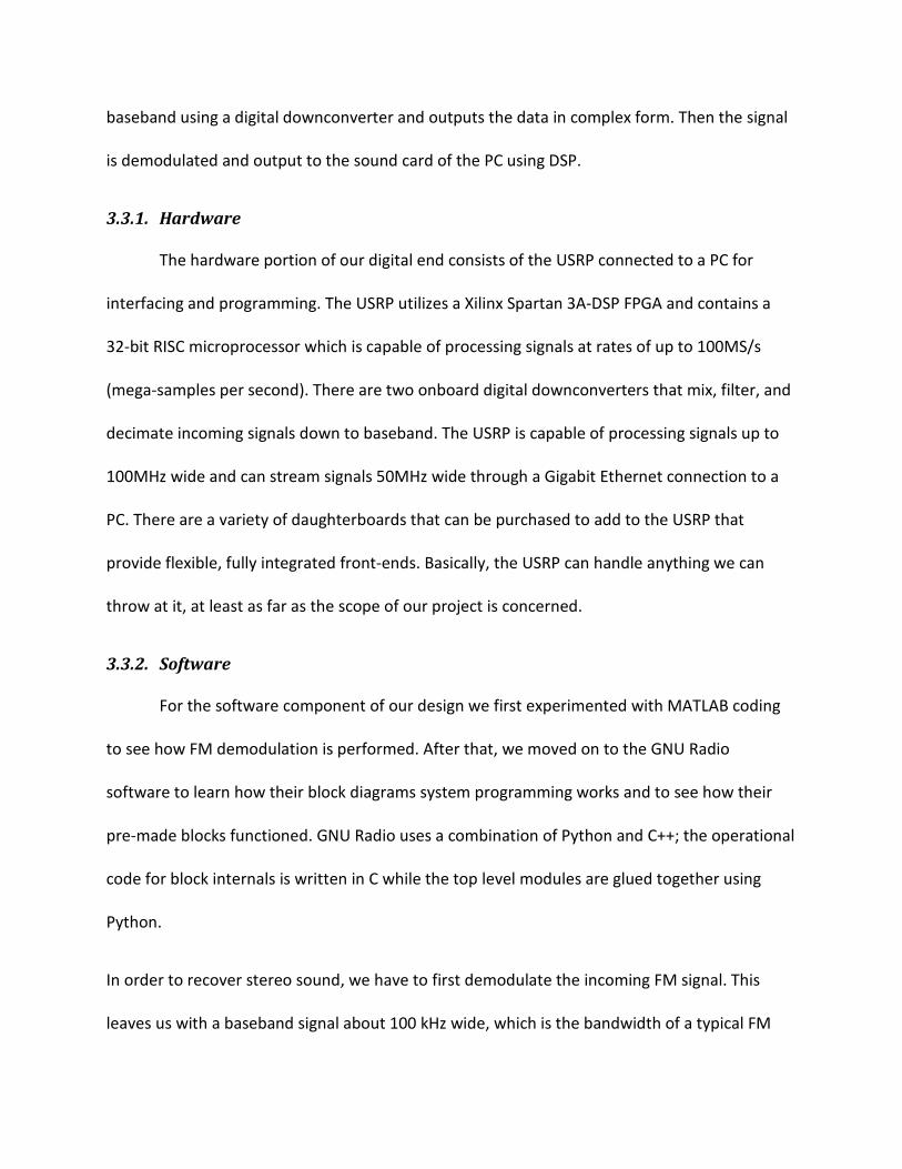
88.1MHz signal at -20dBm and observed the output was at -1.17dB for a gain of about 19dB.
This is shown in the following figure along with the first spur generated by the amplifier
nonlinearities.
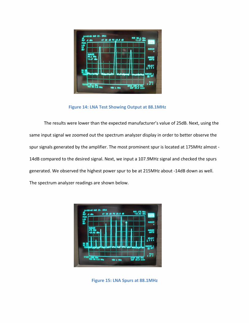
Figure 14: LNA Test Showing Output at 88.1MHz
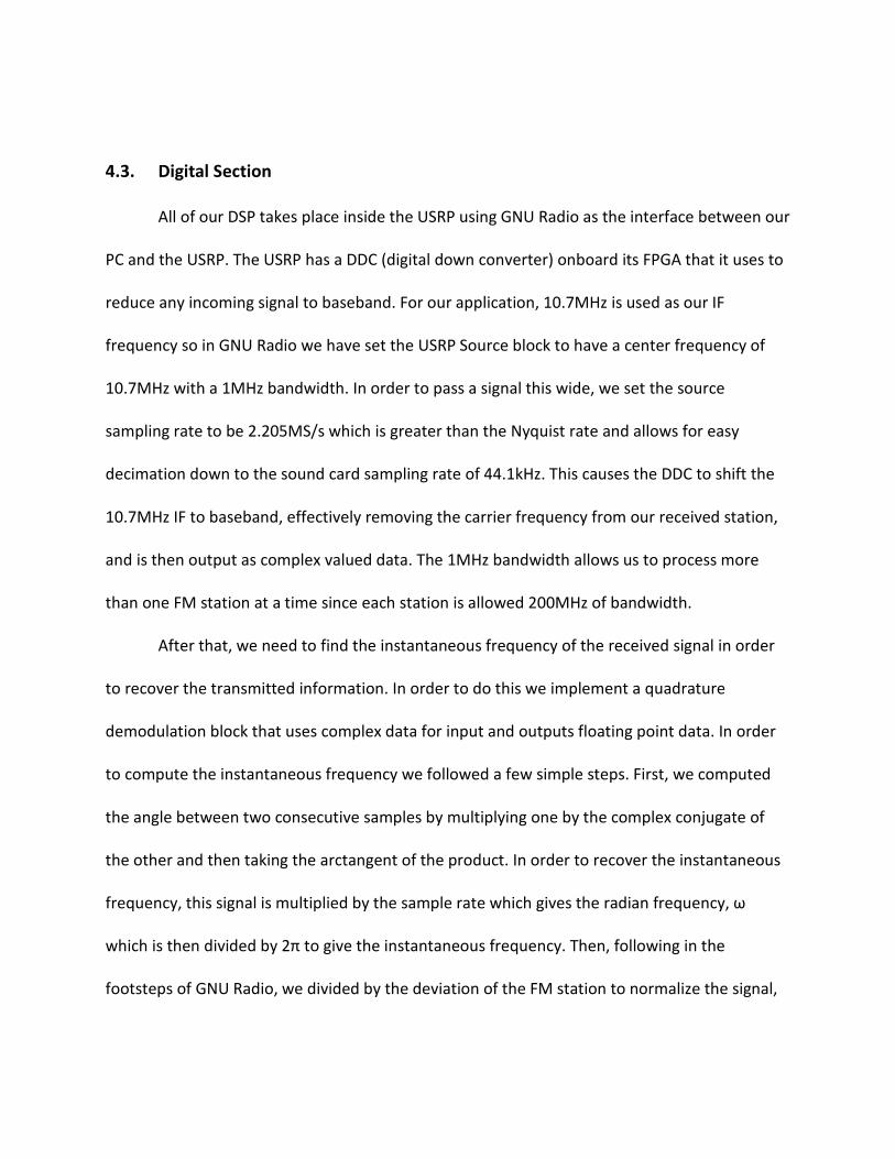
The results were lower than the expected manufacturer’s value of 25dB. Next, using the
same input signal we zoomed out the spectrum analyzer display in order to better observe the
spur signals generated by the amplifier. The most prominent spur is located at 175MHz almost -
14dB compared to the desired signal. Next, we input a 107.9MHz signal and checked the spurs
generated. We observed the highest power spur to be at 215MHz about -14dB down as well.
The spectrum analyzer readings are shown below.
Figure 15: LNA Spurs at 88.1MHz

Figure 16: LNA Spurs at 107.9MHz
5.1.2. Bandpass Filter (SXBP-100)
This is our main bandpass filter that receives the signal from the RAMP. Its purpose is to
limit undesired signal powers outside of the FM band. We only needed to confirm the
manufacturer’s data for the part resembled the observed results. First, we input an 88MHz
signal at 0dBm to measure the low end passband attenuation. We observed a loss of about a
2dB at this frequency. Next, we input a 108MHz signal at 0dBm to measure the high end
passband attenuation. We observed a loss of about 2dB here as well. The results we obtained
were consistent with the data sheet for the part. The spectrum analyzer readings are shown in
the two figures below.

Figure 17: Bandpass Filter Output for 88MHz
Figure 18: Bandpass Filter Output for 108MHz
5.1.3. Lowpass Filter (SXLP-95)
This is a lowpass filter that we decided to implement in our design to make up for the
SXBP’s slightly lower attenuation of the higher out-of-band frequencies. The testing for this
filter was much the same as for the SXBP-100; we needed to check the filter’s real world
performance. We fed the filter with a 108.1MHz signal at 0dBm and observed a loss of 3dB. We
then input a 129.4MHz signal at 0dBm to measure the high end image frequency attenuation.

We observed a loss of about 27dB. This closely resembled the data sheet specifications. The
spectrum analyzer readings are shown in the figures below.
Figure 19: Lowpass Filter Output at 108.1MHz
Figure 20: Lowpass Filter Output at 129.4MHz
5.1.4. Voltage Controlled Oscillator (ZOS-150)
This is the VCO chosen to provide our system with the necessary range of LO
frequencies. Its output operating range is 75MHz to 150MHz. For testing, we used a DC power
supply connected to the tuning input to find the exact voltages needed to generate our range
of LO frequencies. We found that an input voltage of 5.77V would produce 98.7MHz which is
our low end LO frequency. Since we were planning on using 9V batteries for our power supply,
we are limited on the high end to about 9.6V, but chose conservatively to check the output for
a 9.05V input.
We observed 118MHz at the VCO output which is only 0.7MHz shy of the highest
frequency needed for the highest FM station. These values were similar to the data provided by
the manufacturer. The spurs for each input are listed in the following table. Keep in mind there
is a 20dB attenuation provided by the analyzer itself.
Table 1: VCO Analysis
VCO Spur Analysis
Input Output Spur 1 Spur 2 Spur 3 Spur 4
5.77V 98.7MHz
-7dB
197.5MHz
-33dB
297.5MHz
-28dB
395MHz
-39dB
493.8MHz
-45dB
9.05V 118MHz
-7dB
235MHz
-37dB
355MHz
-27dB
473MHz
-39dB
593MHz
-45dB
5.1.5. Frequency Mixer (ZX05-1MHW)
This is the mixer we chose for our design to mix the incoming RF signal and the LO signal
provided by the VCO down to our chosen IF of 10.7MHz. It has a range of operation from
0.5MHz to 600MHz. We decided to test the mixer with an RF input of 98.7MHz, which is the
middle of the FM band, and an LO frequency of 108.7MHz. This should give an IF output of
10MHz. Our results are summarized in the table below.
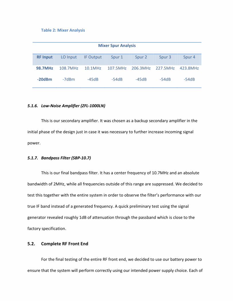
Table 2: Mixer Analysis
Mixer Spur Analysis
RF Input LO Input IF Output Spur 1 Spur 2 Spur 3 Spur 4
98.7MHz
-20dBm
108.7MHz
-7dBm
10.1MHz
-45dB
107.5MHz
-54dB
206.3MHz
-45dB
227.5MHz
-54dB
423.8MHz
-54dB
5.1.6. Low-Noise Amplifier (ZFL-1000LN)
This is our secondary amplifier. It was chosen as a backup secondary amplifier in the
initial phase of the design just in case it was necessary to further increase incoming signal
power.
5.1.7. Bandpass Filter (SBP-10.7)
This is our final bandpass filter. It has a center frequency of 10.7MHz and an absolute
bandwidth of 2MHz, while all frequencies outside of this range are suppressed. We decided to
test this together with the entire system in order to observe the filter’s performance with our
true IF band instead of a generated frequency. A quick preliminary test using the signal
generator revealed roughly 1dB of attenuation through the passband which is close to the
factory specification.
5.2. Complete RF Front End
For the final testing of the entire RF front end, we decided to use our battery power to
ensure that the system will perform correctly using our intended power supply choice. Each of
the parts selected works as expected. One of the amplifiers that we used need to be replaced
because it was damaged at the time of assembling the receiver. The antenna works properly as
we expected. The entire system works as we expected.
6. Final Scope of Work Statement
The project accomplishes the objectives anticipated in the proposal. We were able to
design, build and test a radio receiver that receives an FM band between 88-108 MHz, center
the station to an IF of 10.7 MHz and processes using the USRP. Also it performs our main goal
which is to recover stereo audio. The timeline propose to complete the design, building and
testing process were follow as detailed in the proposal.
6.1. Task to be done
The main goal of this design is to build a front end receiver that will be able to receive
any FM station and with further digital signal processing, using the USRP, recover full stereo
recording. The intent to recovering more than one station at a time, this goal can be done with
a deeper research of the USRP function.
Besides the modification suggested above, the hardware design of this project needs a
little modification from this point on. Further improvements that can be done to this design can
be summarizing in future digital processing work.
6.2 Lessons Learned
The entire process of building our receiver taught us important procedures and
calculations that need to be done in order to successfully build a prototype for a radio.
In order to build our radio front end we learned how the selection of the different parts
will influence the final product. A frequency plan needs to be done, which explains in detail
what RF, IF and LO frequencies the system will need. This frequency plan helped us to select the
adequate parts needed for the design. A cascade and mixer analysis needs to be done. During
the assembly of our front end, we encounter a few problems with the circuitry of our power
supply and malfunction of the parts. We were able to learn how to design a circuitry to power
our voltage control oscillator and our amplifiers to guarantee a better performance of the
receiver.
As stated in the class syllabus of our digital radio class we were able to understand how
the Universal Software Radio Peripheral (USRP) can be used as a FM radio receiver, as testing
equipment and as a digital signal processing tool. We learned that to be able to perform dual-
channel recovery we need to rebuild our hardware design and to implement the USRP with a
deeper knowledge of it.
6.3 Suggestions for future works
Due to time constrains we were able to recover one station at a time; however we were
not able to perform dual-channel recovery. We learned that this could have been done through
a different design of our front end by adding more filters. Those filters will have been able to
capture each of one of the stations that later we want to recover. Even though, this design was
one of our pre-design options, we did not implement because it will need a big amount of
filters. In addition, we deduce that this can be done with the help of the USRP. An extensive

research of the USRP can be done to be able to use this digital signal processing tool to perform
dual-channel recovery.
Another improvement that we observe can be done due to recover dual-channel
stations is to implement a different made code that can be added to the USRP interface.
6.4 Project Specifics
Due to budget limitation we utilized parts that already were able from previous digital
radio class. Some of these parts have a broad frequency range that our design needs and
demand a different voltage supply. Because of that we could not be able to restrain the power
consumption of one of our amplifiers, so we have to include two different power supplies. For
simplicity and the addition of a new amplifier we rebuilt or power circuitry different times to
meet our constraints.
8. Cost Estimation
For this project we have a limited budget of 500 dollars. Dr. Gunther allows us to use
some parts from previous classes and financially support us with the purchase of others parts to
build the front end receiver. High-cost items such as the computer and the USRP were provided
for us from the Electrical Engineering Department. The following is an actual budget that details
the cost of the parts of this project.

Table 3. Budget
Item Quantity Price per Unit Total Price
Antenna 1 $3.00 $3.00
ZFL-1000 LN 1 $89.95 $89.95
Band Pass Filter (SXBP-100) 1 $15.95 $15.95
Evaluation Board (TB-368) 2 $34.95 $69.90
Low Pass Filter (SXLP-95) 1 $11.45 $11.45
Evaluation Board (TB-10) 1 $29.95 $29.95
Low Noise Amplifier (RAMP-33LN) 1 $19.95 $19.95
ZOD-150 1 $119.95 $119.95
ZXO5-1MHW 1 $39.95 $39.95
SBP-10.7 1 $42.95 $42.95
USRP 2010N 1 $1500.00 $1500.00
PC 1 $500.00 $500.00
Batteries 9V, 4 pack 4 $9.50 $38.00
Board 1 $5.00 $5.00
Miscellaneous $60.00 $60.00
Total $2546.00
8.1 Other Issues
Over the course of our project we ran into a couple of unforeseen difficulties the most
prominent of which was figuring out power delivery for each of the components. We initially

tried to use a typical 7805 linear regulator which worked initially except for our VCO which had
a lot of signal drift on its output due to the slight voltage swing appearing on the output of the
regulator. We managed to find integrated circuit (IC) voltage regulator chips that would meet
our needs in the form of National Semiconductor’s LM723C which can be configured in a
number of operating modes. We used an 18.5V computer power supply connected to four of
these regulators to supply all of our operating voltages. We are using two regulators as 15V
supplies for the amplifiers, a 12V regulator for our VCO supply, and a 5V regulator for VCO
tuning. These parts have no observable drift which allows for very precise tuning of our VCO as
an additional bonus.
The original regulators also seemed to play a part in three separate part failures, both of
our amplifiers and our VCO, due to possible lack of foresight on our part to regulate the current
being supplied to our devices even though our initial measurements showed current draws
within acceptable limits. Due to this, we had to find replacement parts that would still work
acceptably for our design within a very short time frame. We managed to find a new VCO and
two more amplifiers that, while not as effective as our original part selection, still allow us to
have a functional FM receiver.
9. Project Management Summary
Our team consists of three senior students majoring in Electrical Engineering. At the
same time, we are current students of the Digital Radio class, in which we were able to obtain
the necessary knowledge and resources required to build the front end prototype and the
necessary dexterity to effectively utilize the USRP to demodulate.

Some of the challenging tasks that we encounter doing this project were the research
that we have to put into the first weeks of class and the testing period. The first two months of
this semester we learned the necessary tools, both for hardware and software, to effectively
design the receiver. A fair estimate of hours that each of us spend on this project per week goes
around eight to ten hours. We spend an entire semester of sixteen weeks total working in this
project; this gives a total of 128 hours per person and 384 hours altogether.
9.1 Tasks
The following is a list that contains the tasks that were been done during the development
of this project:
1) Research
a. Information about the USRP
2) Design
a. Propose a Frequency plan
b. Allocate the necessary LO and IF
c. Select parts needed
3) Building Process
a. Construct front end receiver
b. Power constraints
c. Testing
4) USRP
5) Documentation
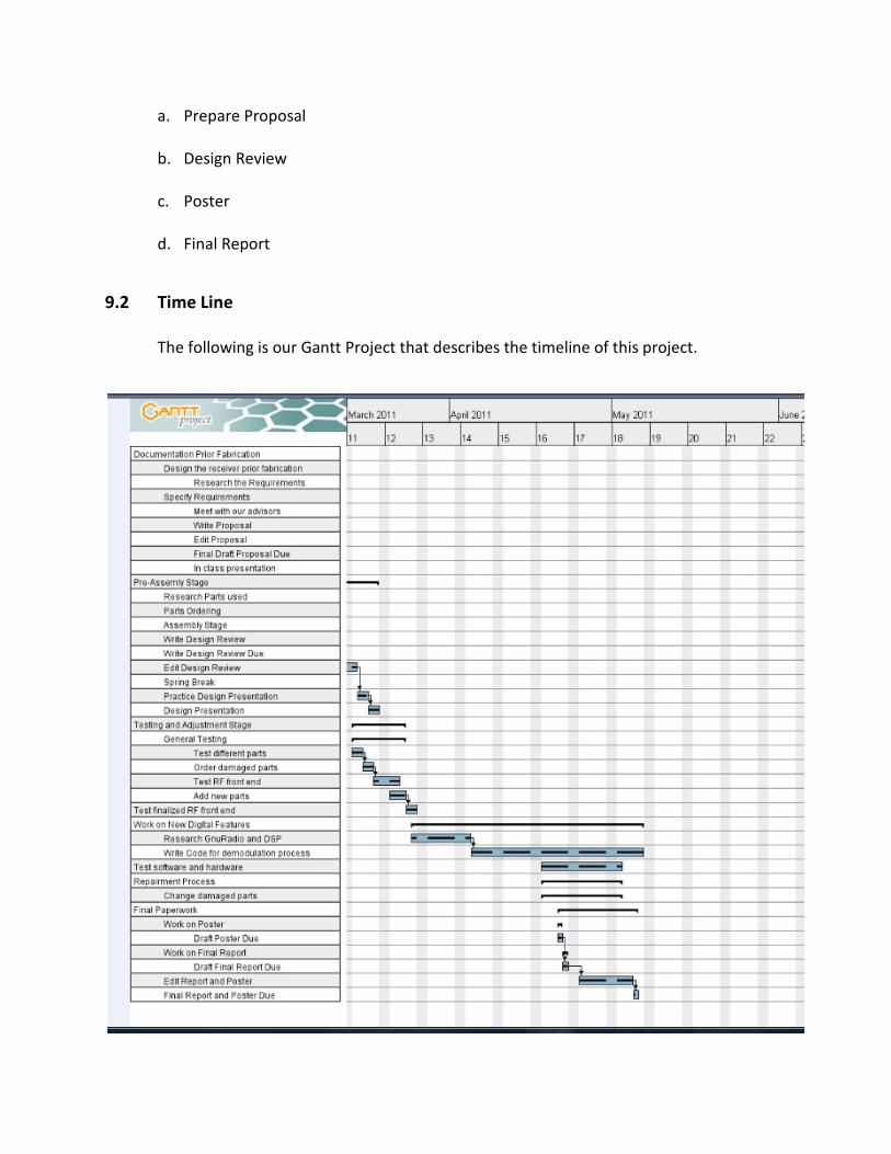
a. Prepare Proposal
b. Design Review
c. Poster
d. Final Report
9.2 Time Line
The following is our Gantt Project that describes the timeline of this project.

10. Conclusion
In conclusion, this project was to research the different types of architectures and pick
the one that we felt was the best one. Using that architecture that we picked we needed to
build a simple radio receiver front end that receives the entire FM band and send a couple
signals to the USRP so we can demodulate them at the same time and send them out to the PC.
With all of the complications that we encountered we were unable to demodulated and send
out two different ones at the same time. So instead we were able to recover the stereo portion
of a single station and have that played through the speakers. We successfully have a working
prototype and the schematics are included in the upper portion of the document. The budget
for this project was $500.00. If there are any questions or concerns about this project feel free
to contact us at any time.
Matthew Fox Paul Gilbert Raysa Suazo [email protected] [email protected] [email protected]
Cell: 435-232-4501 Cell: 801-391-9443 Cell: 435-512-3933

Appendix