Embed Size (px)
Citation preview
DIC-Lec2 [email protected] 1
Digital Integrated CircuitsLecture 2: MIPS Processor Example
Chih-Wei Liu
VLSI Signal Processing LAB
National Chiao Tung University
DIC-Lec2 [email protected] 2
Outline
Design Partitioning
MIPS Processor ExampleArchitecture
Microarchitecture
Logic Design
Circuit Design
Physical Design
Fabrication, Packaging, Testing
DIC-Lec2 [email protected] 5
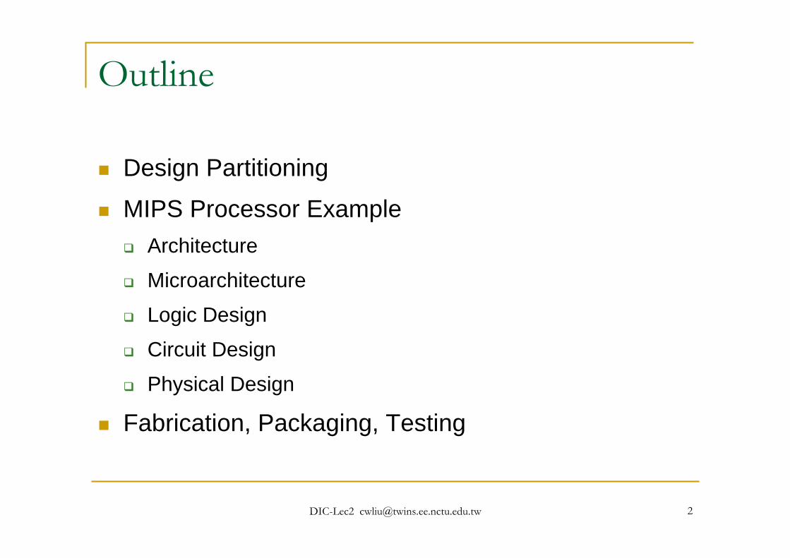
Coping with Complexity
How to design System-on-Chip?Many millions (even billions!) of transistors
Tens to hundreds of engineers
Structured Design
Design Partitioning
DIC-Lec2 [email protected] 6
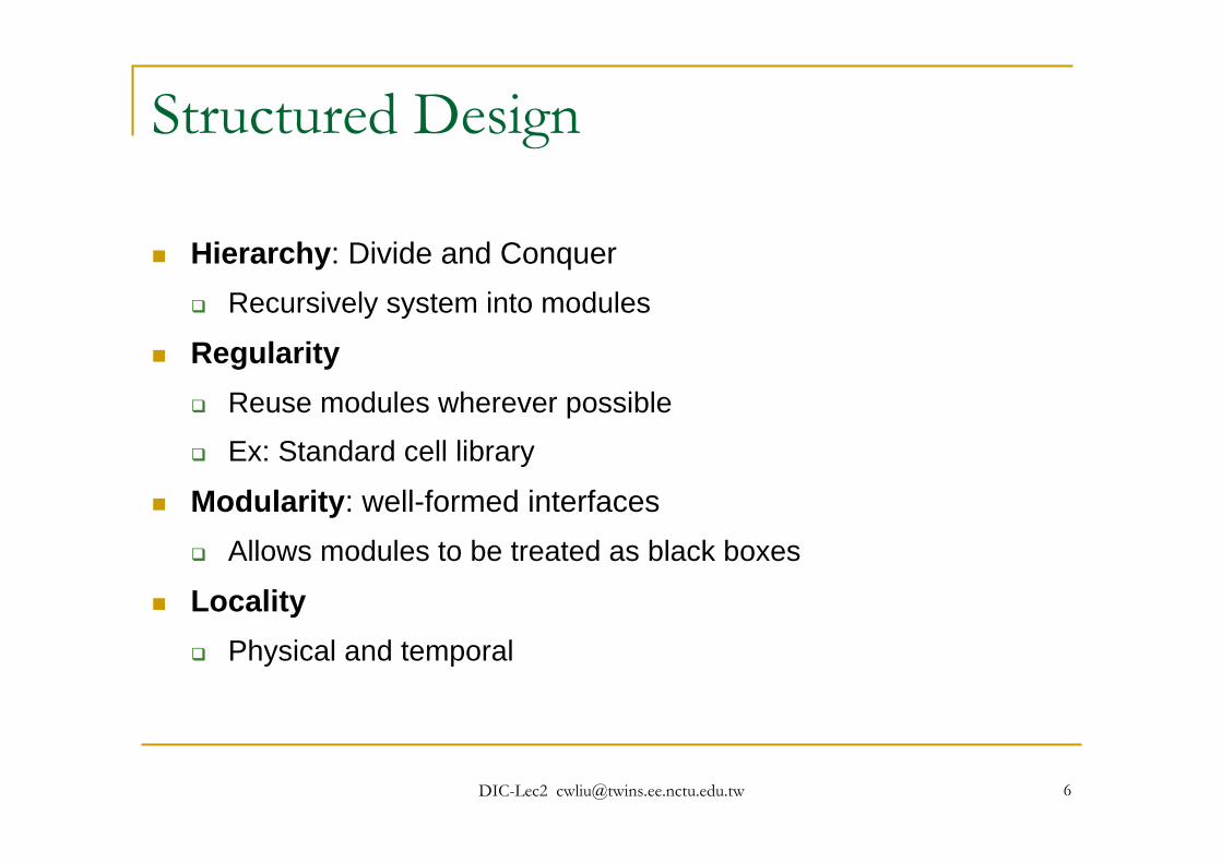
Structured Design
Hierarchy: Divide and ConquerRecursively system into modules
RegularityReuse modules wherever possible
Ex: Standard cell library
Modularity: well-formed interfacesAllows modules to be treated as black boxes
LocalityPhysical and temporal
DIC-Lec2 [email protected] 7
Design Partitioning
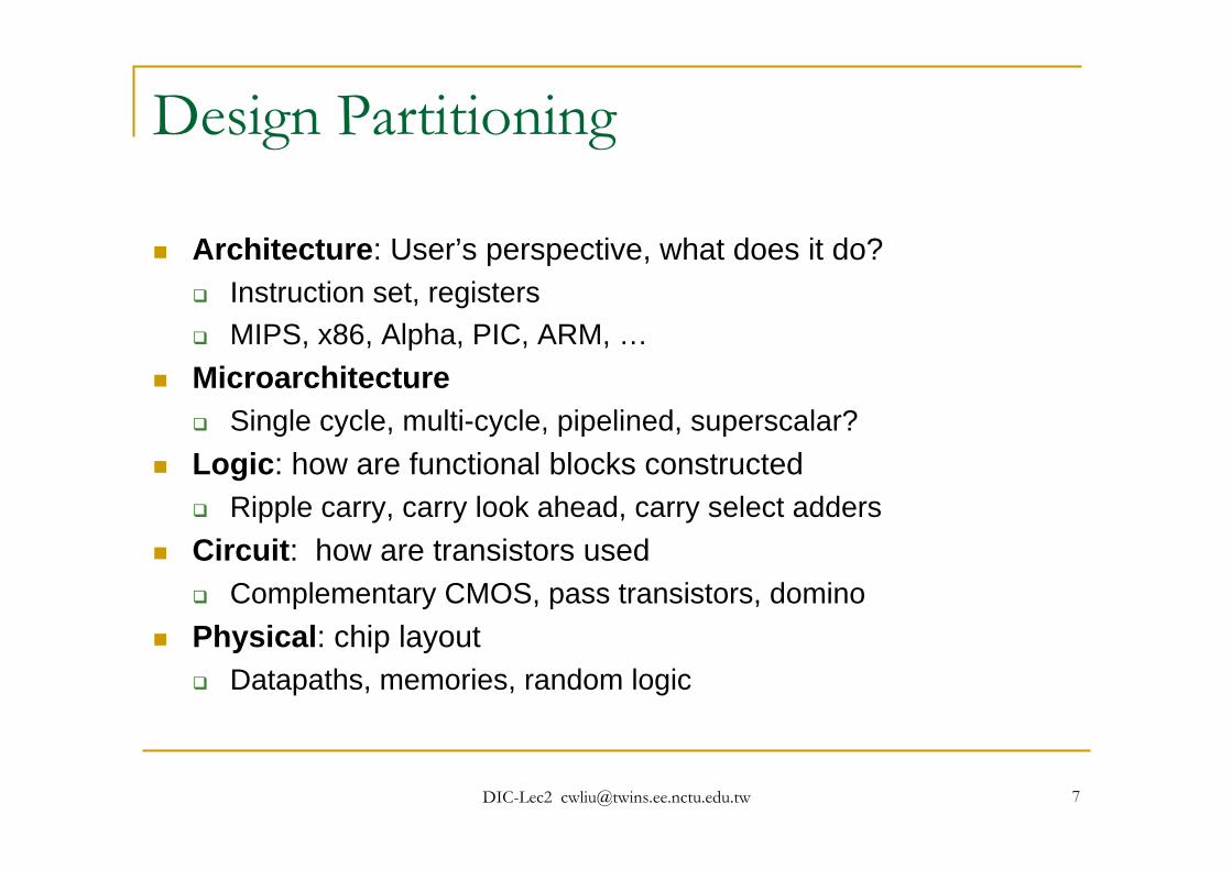
Architecture: User’s perspective, what does it do?Instruction set, registersMIPS, x86, Alpha, PIC, ARM, …
MicroarchitectureSingle cycle, multi-cycle, pipelined, superscalar?
Logic: how are functional blocks constructedRipple carry, carry look ahead, carry select adders
Circuit: how are transistors usedComplementary CMOS, pass transistors, domino
Physical: chip layoutDatapaths, memories, random logic
DIC-Lec2 [email protected] 9
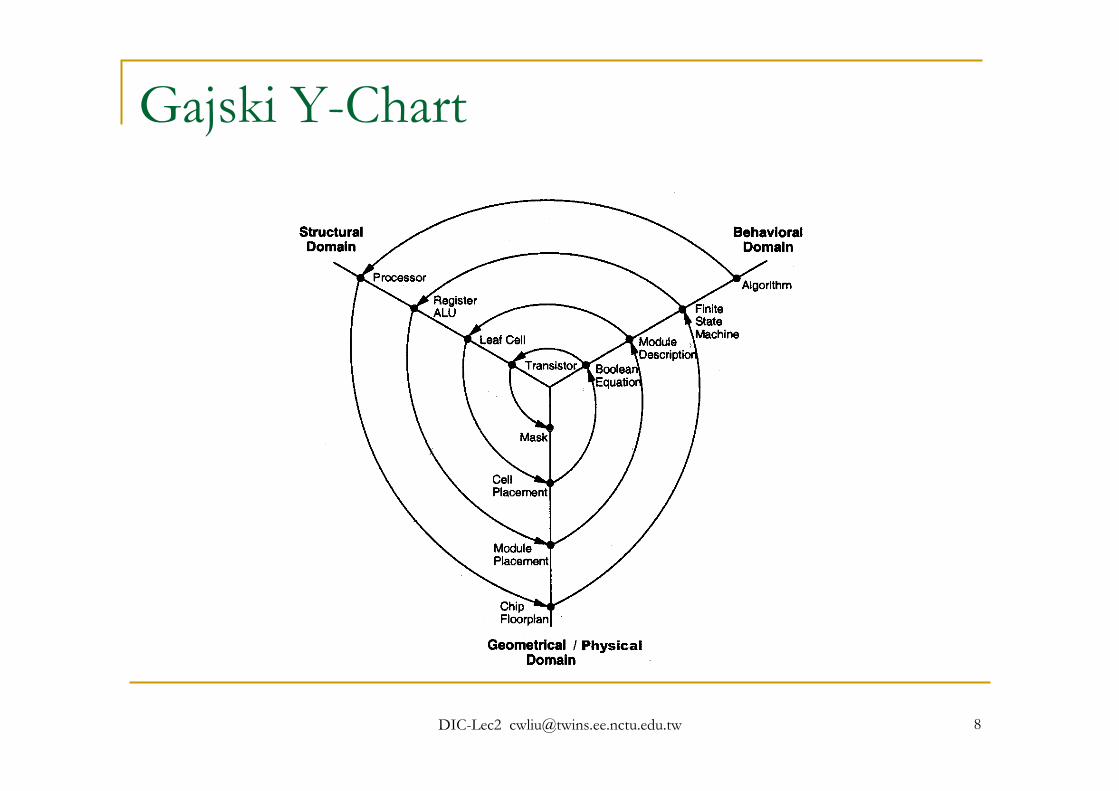
MIPS Architecture
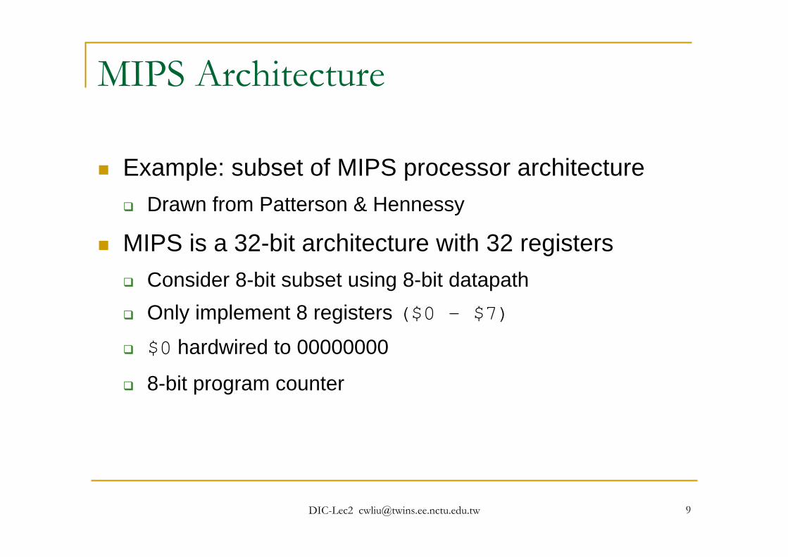
Example: subset of MIPS processor architectureDrawn from Patterson & Hennessy
MIPS is a 32-bit architecture with 32 registersConsider 8-bit subset using 8-bit datapathOnly implement 8 registers ($0 - $7)
$0 hardwired to 00000000
8-bit program counter
DIC-Lec2 [email protected] 11
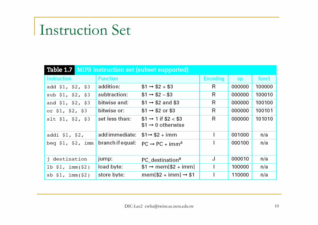
Instruction Encoding
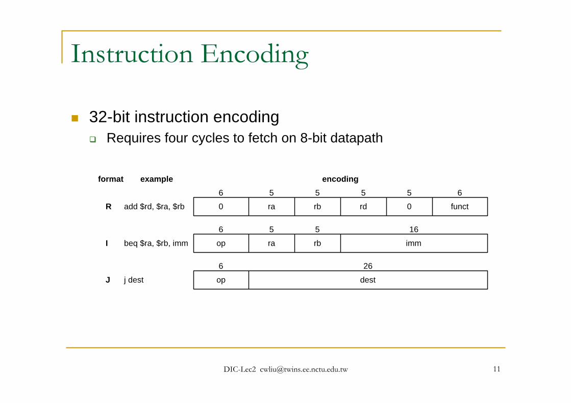
32-bit instruction encodingRequires four cycles to fetch on 8-bit datapath
format example encoding
R
I
J
0 ra rb rd 0 funct
op
op
ra rb imm
6
6
6
65 5 5 5
5 5 16
26
add $rd, $ra, $rb
beq $ra, $rb, imm
j dest dest
DIC-Lec2 [email protected] 12
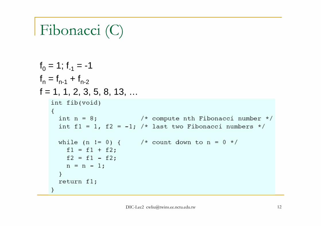
Fibonacci (C)
f0 = 1; f-1 = -1fn = fn-1 + fn-2
f = 1, 1, 2, 3, 5, 8, 13, …
DIC-Lec2 [email protected] 13
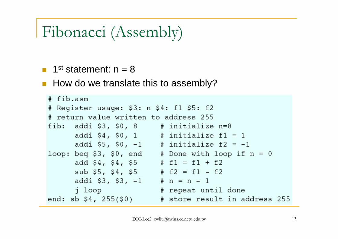
Fibonacci (Assembly)
1st statement: n = 8How do we translate this to assembly?
DIC-Lec2 [email protected] 14
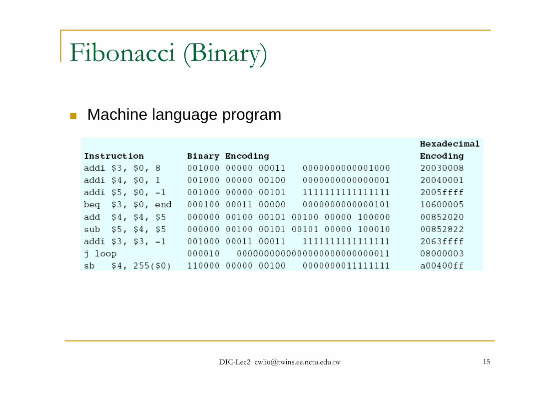
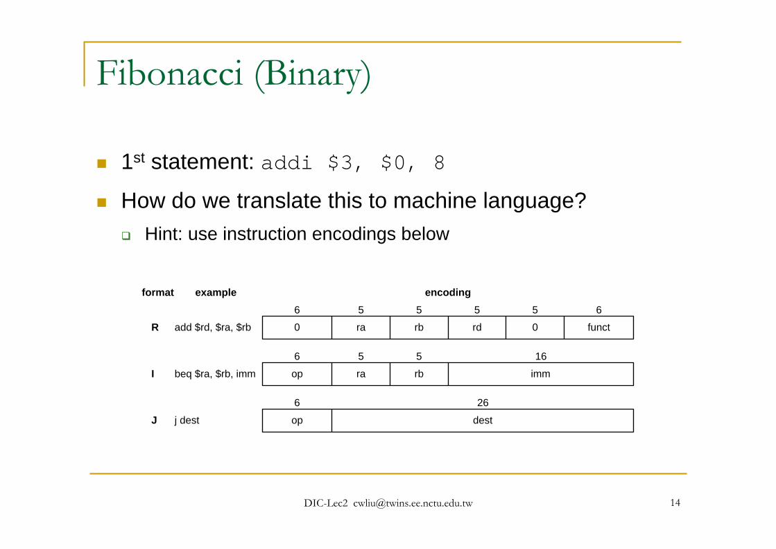
Fibonacci (Binary)
1st statement: addi $3, $0, 8
How do we translate this to machine language?Hint: use instruction encodings below
format example encoding
R
I
J
0 ra rb rd 0 funct
op
op
ra rb imm
6
6
6
65 5 5 5
5 5 16
26
add $rd, $ra, $rb
beq $ra, $rb, imm
j dest dest
DIC-Lec2 [email protected] 16
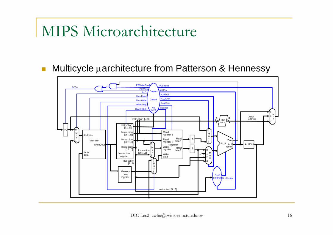
MIPS Microarchitecture
Multicycle μarchitecture from Patterson & Hennessy
PCMux
0
1
RegistersWriteregister
Writedata
Readdata 1
Readdata 2
Readregister 1
Readregister 2
Instruction[15: 11]
Mux
0
1
Mux
0
1
1
Instruction[7: 0]
Instruction[25 : 21]
Instruction[20 : 16]
Instruction[15 : 0]
Instructionregister
ALUcontrol
ALUresult
ALUZero
Memorydata
register
A
B
IorD
MemRead
MemWrite
MemtoReg
PCWriteCond
PCWrite
IRWrite[3:0]
ALUOp
ALUSrcB
ALUSrcA
RegDst
PCSource
RegWriteControl
Outputs
Op[5 : 0]
Instruction[31:26]
Instruction [5 : 0]
Mux
0
2
JumpaddressInstruction [5 : 0] 6 8
Shiftleft 2
1
1 Mux
0
32
Mux
0
1ALUOut
MemoryMemData
Writedata
Address
PCEn
ALUControl
DIC-Lec2 [email protected] 17
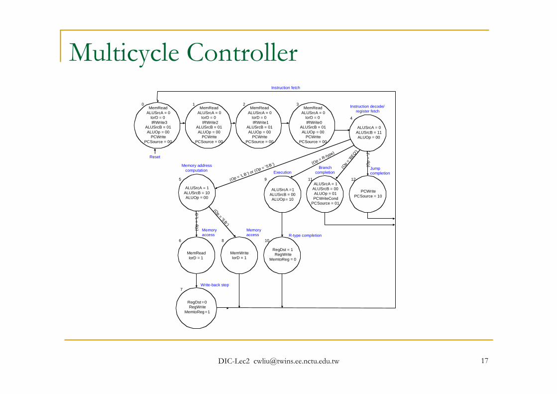
Multicycle Controller
PCWritePCSource = 10
ALUSrcA = 1ALUSrcB = 00ALUOp = 01PCWriteCond
PCSource = 01
ALUSrcA =1ALUSrcB = 00ALUOp= 10
RegDst = 1RegWrite
MemtoReg = 0MemWriteIorD = 1
MemReadIorD = 1
ALUSrcA = 1ALUSrcB = 10ALUOp = 00
RegDst=0RegWrite
MemtoReg =1
ALUSrcA = 0ALUSrcB = 11ALUOp = 00
MemReadALUSrcA = 0
IorD = 0IRWrite3
ALUSrcB = 01ALUOp = 00
PCWritePCSource = 00
Instruction fetch
Instruction decode/register fetch
Jumpcompletion
BranchcompletionExecution
Memory addresscomputation
Memoryaccess
Memoryaccess R-type completion
Write-back step
(Op = 'LB ') or (Op = 'SB ') (Op = R-type)
(Op = 'B
EQ')
(Op
='J
')
(Op = 'S B')
(Op
='L
B')
7
0
4
121195
1086
Reset
MemReadALUSrcA = 0
IorD = 0IRWrite2
ALUSrcB = 01ALUOp = 00
PCWritePCSource = 00
1MemRead
ALUSrcA = 0IorD = 0IRWrite1
ALUSrcB = 01ALUOp = 00
PCWritePCSource = 00
2MemRead
ALUSrcA = 0IorD = 0IRWrite0
ALUSrcB = 01ALUOp = 00
PCWritePCSource = 00
3
DIC-Lec2 [email protected] 18
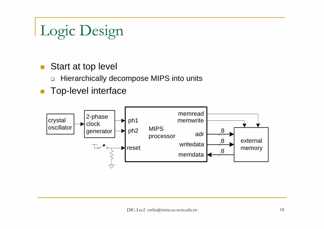
Logic Design
Start at top levelHierarchically decompose MIPS into units
Top-level interface
reset
ph1
ph2
crystaloscillator
2-phaseclockgenerator MIPS
processor adr
writedata
memdata
externalmemory
memreadmemwrite
8
8
8
DIC-Lec2 [email protected] 19
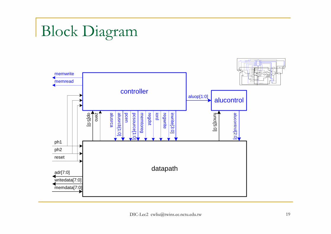
Block Diagram
datapath
controlleralucontrol
ph1
ph2
reset
memdata[7:0]
writedata[7:0]
adr[7:0]
memread
memwrite
op[5:0]
zero
pcen
regwrite
irwrite[3:0]
mem
toreg
iord
pcsource[1:0]
alusrcb[1:0]
alusrca
aluop[1:0]
regdst
funct[5:0]
alucontrol[2:0]
PCMux
0
1
RegistersWriteregister
Writedata
Readdata 1
Readdata 2
Readregister 1
Readregister 2
Instruction[15: 11]
Mux
0
1
Mux
0
1
1
Instruction[7: 0]
Instruction[25 : 21]
Instruction[20 : 16]
Instruction[15 : 0]
Instructionregister
ALUcontrol
ALUresult
ALUZero
Memorydata
register
A
B
IorD
MemRead
MemWrite
MemtoReg
PCWriteCond
PCWrite
IRWrite[3:0]
ALUOp
ALUSrcB
ALUSrcA
RegDst
PCSource
RegWriteControl
Outputs
Op[5 : 0]
Instruction[31:26]
Instruction [5 : 0]
Mux
0
2
JumpaddressInstruction [5 : 0] 6 8
Shiftleft 2
1
1 Mux
0
32
Mux
0
1ALUOut
MemoryMemData
Writedata
Address
PCEn
ALUControl
DIC-Lec2 [email protected] 20
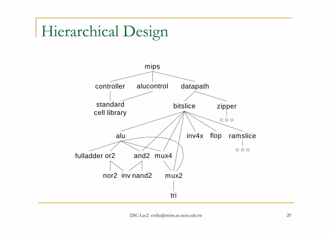
Hierarchical Design
mips
controller alucontrol datapath
standardcell library
bitslice zipper
alu
and2
flopinv4x
mux2
mux4
ramslice
fulladder
nand2nor2
or2
inv
tri
DIC-Lec2 [email protected] 21
HDLs
Hardware Description LanguagesWidely used in logic design
Verilog and VHDL
Describe hardware using codeDocument logic functions
Simulate logic before building
Synthesize code into gates and layoutRequires a library of standard cells
DIC-Lec2 [email protected] 22
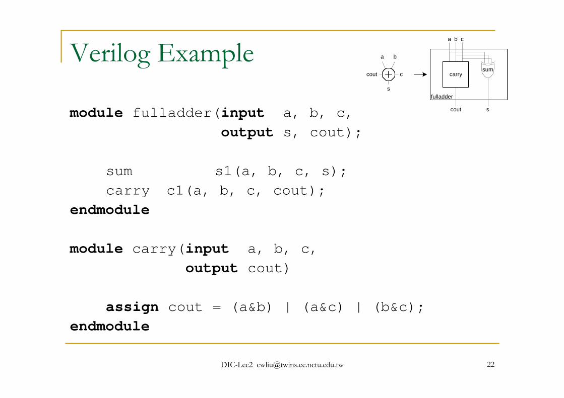
Verilog Example
module fulladder(input a, b, c, output s, cout);
sum s1(a, b, c, s);carry c1(a, b, c, cout);
endmodule
module carry(input a, b, c, output cout)
assign cout = (a&b) | (a&c) | (b&c);endmodule
a b
c
s
cout carrysum
s
a b c
cout
fulladder
DIC-Lec2 [email protected] 23
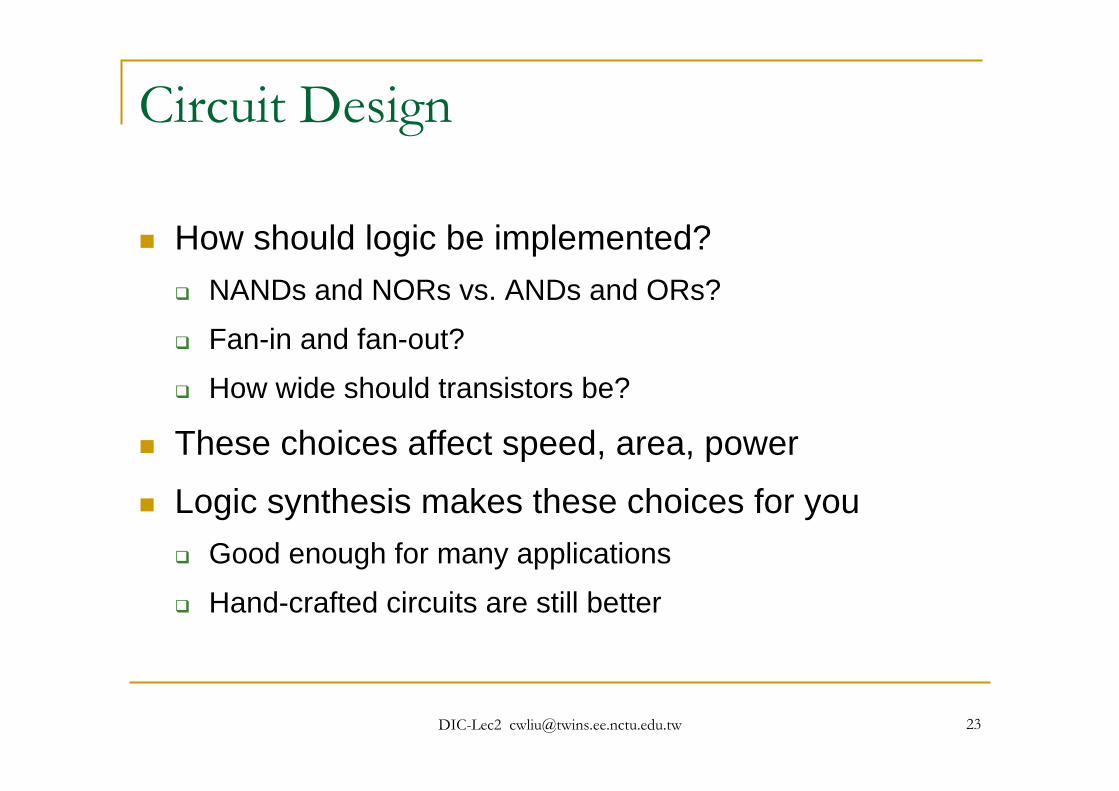
Circuit Design
How should logic be implemented?NANDs and NORs vs. ANDs and ORs?
Fan-in and fan-out?
How wide should transistors be?
These choices affect speed, area, power
Logic synthesis makes these choices for youGood enough for many applications
Hand-crafted circuits are still better
DIC-Lec2 [email protected] 24
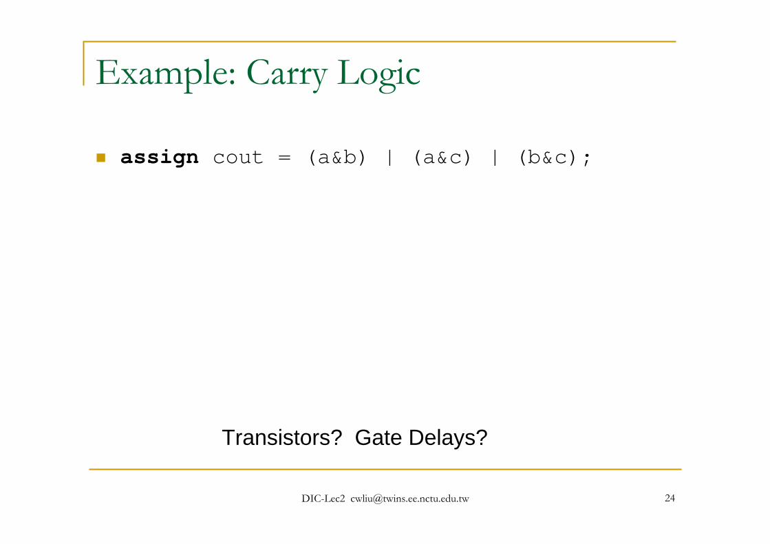
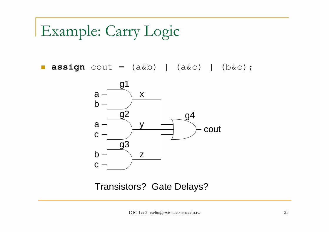
Example: Carry Logic
assign cout = (a&b) | (a&c) | (b&c);
Transistors? Gate Delays?
DIC-Lec2 [email protected] 25
Example: Carry Logic
assign cout = (a&b) | (a&c) | (b&c);
ab
ac
bc
cout
x
y
z
g1
g2
g3
g4
Transistors? Gate Delays?
DIC-Lec2 [email protected] 26
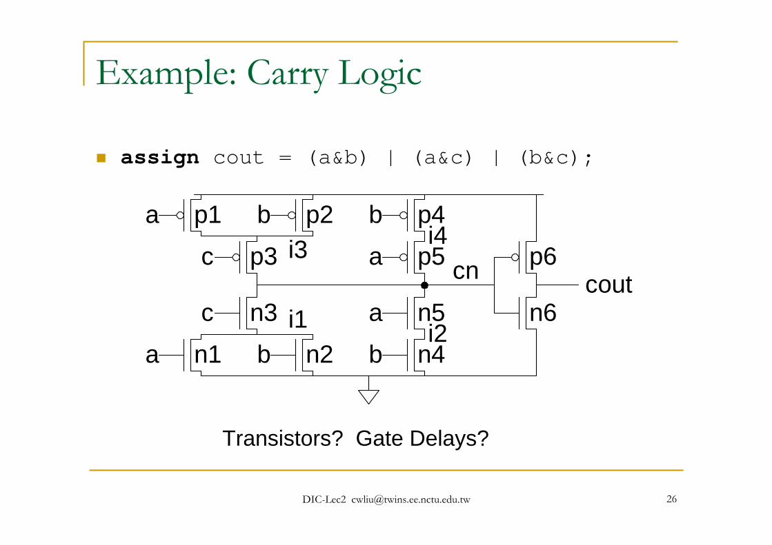
Example: Carry Logic
assign cout = (a&b) | (a&c) | (b&c);
Transistors? Gate Delays?
a b
c
c
a b
b
a
a
b
coutcn
n1 n2
n3
n4
n5 n6
p6p5
p4
p3
p2p1
i1
i3
i2
i4
DIC-Lec2 [email protected] 27
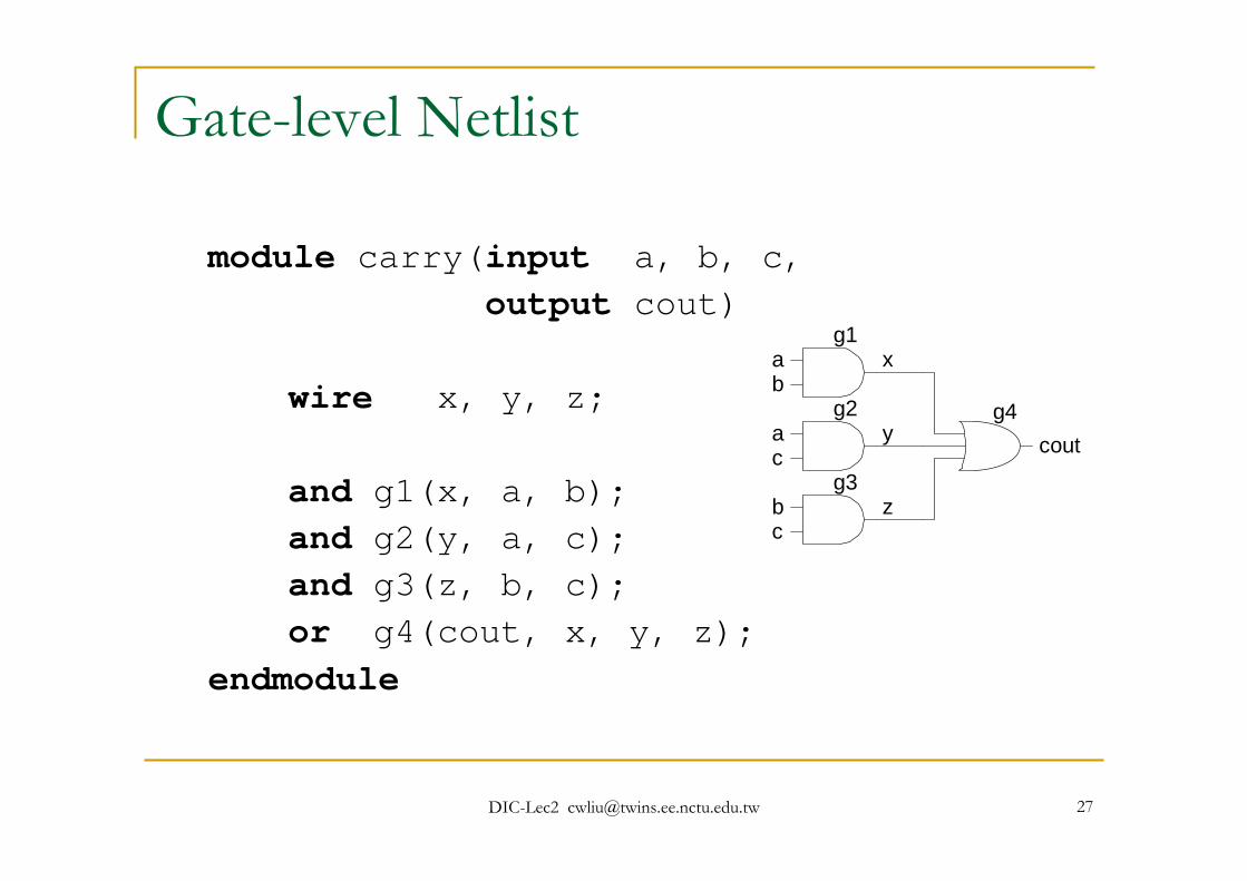
Gate-level Netlist
module carry(input a, b, c, output cout)
wire x, y, z;
and g1(x, a, b);and g2(y, a, c);and g3(z, b, c);or g4(cout, x, y, z);
endmodule
ab
ac
bc
cout
x
y
z
g1
g2
g3
g4
DIC-Lec2 [email protected] 28
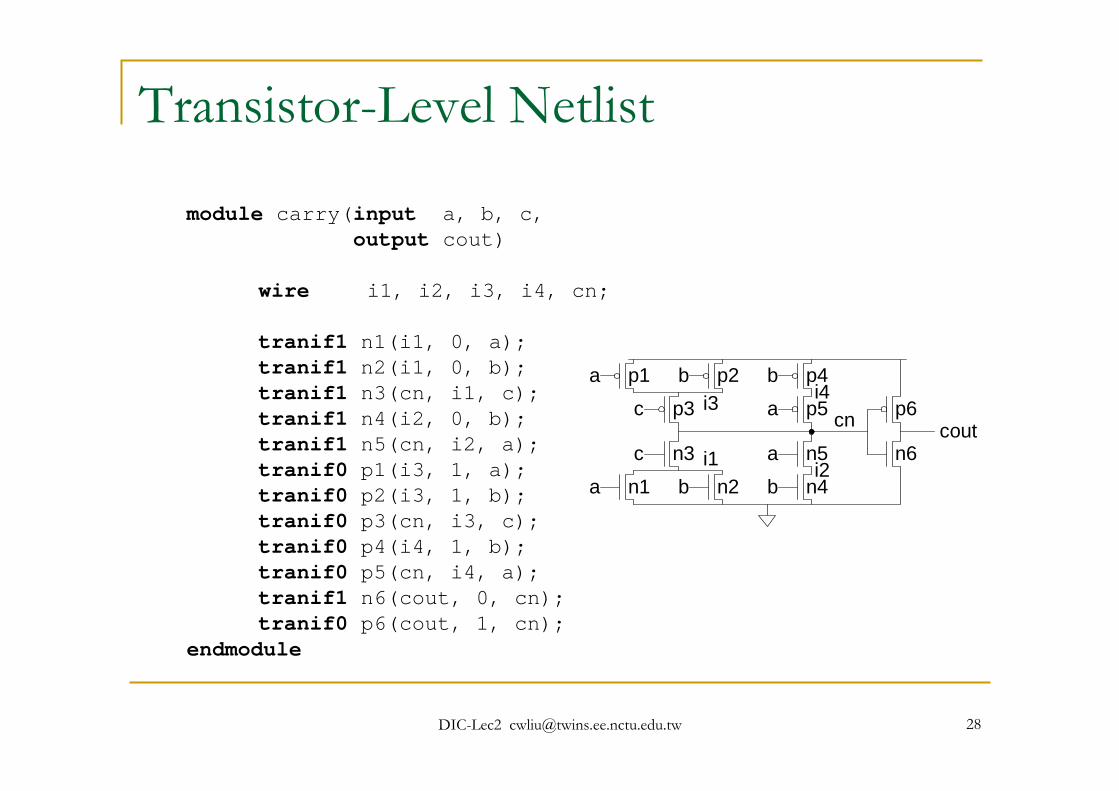
Transistor-Level Netlist
a b
c
c
a b
b
a
a
b
coutcn
n1 n2
n3
n4
n5 n6
p6p5
p4
p3
p2p1
i1
i3
i2
i4
module carry(input a, b, c, output cout)
wire i1, i2, i3, i4, cn;
tranif1 n1(i1, 0, a);tranif1 n2(i1, 0, b);tranif1 n3(cn, i1, c);tranif1 n4(i2, 0, b);tranif1 n5(cn, i2, a);tranif0 p1(i3, 1, a);tranif0 p2(i3, 1, b);tranif0 p3(cn, i3, c);tranif0 p4(i4, 1, b);tranif0 p5(cn, i4, a);tranif1 n6(cout, 0, cn);tranif0 p6(cout, 1, cn);
endmodule
DIC-Lec2 [email protected] 29
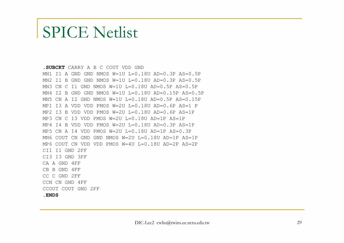
SPICE Netlist
.SUBCKT CARRY A B C COUT VDD GNDMN1 I1 A GND GND NMOS W=1U L=0.18U AD=0.3P AS=0.5PMN2 I1 B GND GND NMOS W=1U L=0.18U AD=0.3P AS=0.5PMN3 CN C I1 GND NMOS W=1U L=0.18U AD=0.5P AS=0.5PMN4 I2 B GND GND NMOS W=1U L=0.18U AD=0.15P AS=0.5PMN5 CN A I2 GND NMOS W=1U L=0.18U AD=0.5P AS=0.15PMP1 I3 A VDD VDD PMOS W=2U L=0.18U AD=0.6P AS=1 PMP2 I3 B VDD VDD PMOS W=2U L=0.18U AD=0.6P AS=1PMP3 CN C I3 VDD PMOS W=2U L=0.18U AD=1P AS=1PMP4 I4 B VDD VDD PMOS W=2U L=0.18U AD=0.3P AS=1PMP5 CN A I4 VDD PMOS W=2U L=0.18U AD=1P AS=0.3PMN6 COUT CN GND GND NMOS W=2U L=0.18U AD=1P AS=1PMP6 COUT CN VDD VDD PMOS W=4U L=0.18U AD=2P AS=2PCI1 I1 GND 2FFCI3 I3 GND 3FFCA A GND 4FFCB B GND 4FFCC C GND 2FFCCN CN GND 4FFCCOUT COUT GND 2FF.ENDS
DIC-Lec2 [email protected] 30
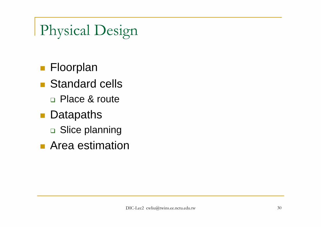
Physical Design
FloorplanStandard cells
Place & routeDatapaths
Slice planningArea estimation
DIC-Lec2 [email protected] 31
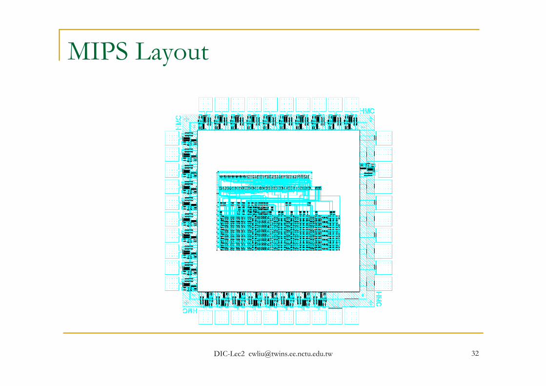
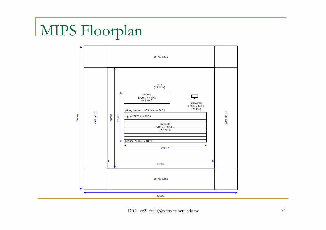
MIPS Floorplan
datapath2700 λ x 1050 λ
(2.8 Mλ2)
alucontrol200 λ x 100 λ
(20 kλ2)
zipper 2700 λ x 250 λ
2700 λ
1690 λ
wiring channel: 30 tracks = 240 λ
mips(4.6 Mλ2)
bitslice 2700 λ x 100 λ
control1500 λ x 400 λ
(0.6 Mλ2)
3500 λ
3500 λ
5000λ
5000 λ
10 I/O pads
10 I/O pads
10 I/O pads
10 I/O pads
DIC-Lec2 [email protected] 33
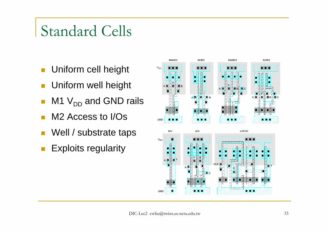
Standard Cells
Uniform cell height
Uniform well height
M1 VDD and GND rails
M2 Access to I/Os
Well / substrate taps
Exploits regularity
DIC-Lec2 [email protected] 34
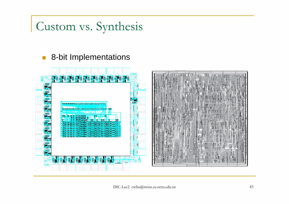
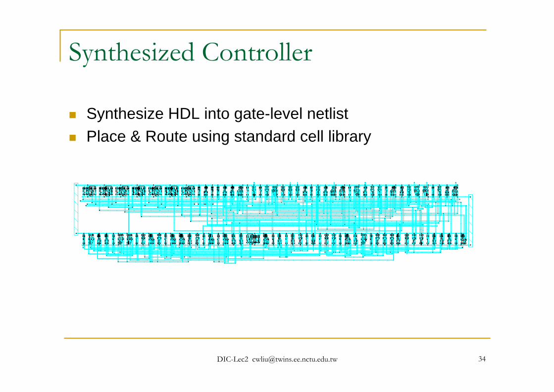
Synthesized Controller
Synthesize HDL into gate-level netlistPlace & Route using standard cell library
DIC-Lec2 [email protected] 35
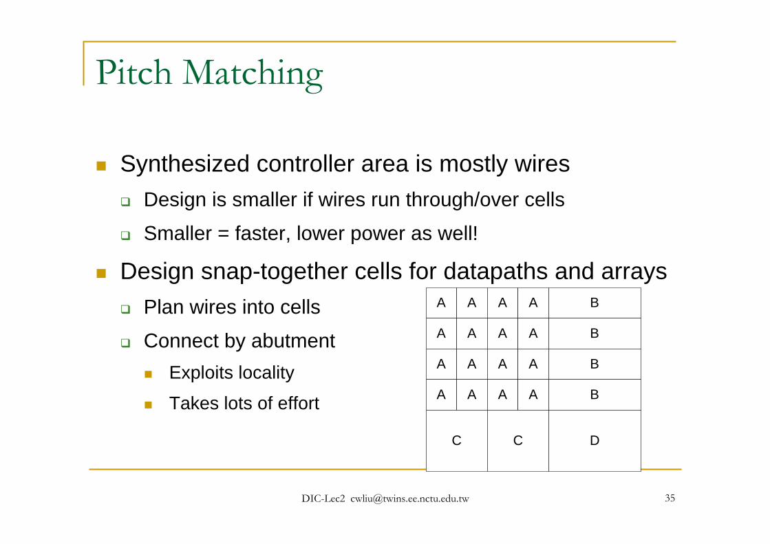
Pitch Matching
Synthesized controller area is mostly wiresDesign is smaller if wires run through/over cells
Smaller = faster, lower power as well!
Design snap-together cells for datapaths and arraysPlan wires into cells
Connect by abutmentExploits locality
Takes lots of effort
A A A A
A A A A
A A A A
A A A A
B
B
B
B
C C D
DIC-Lec2 [email protected] 36
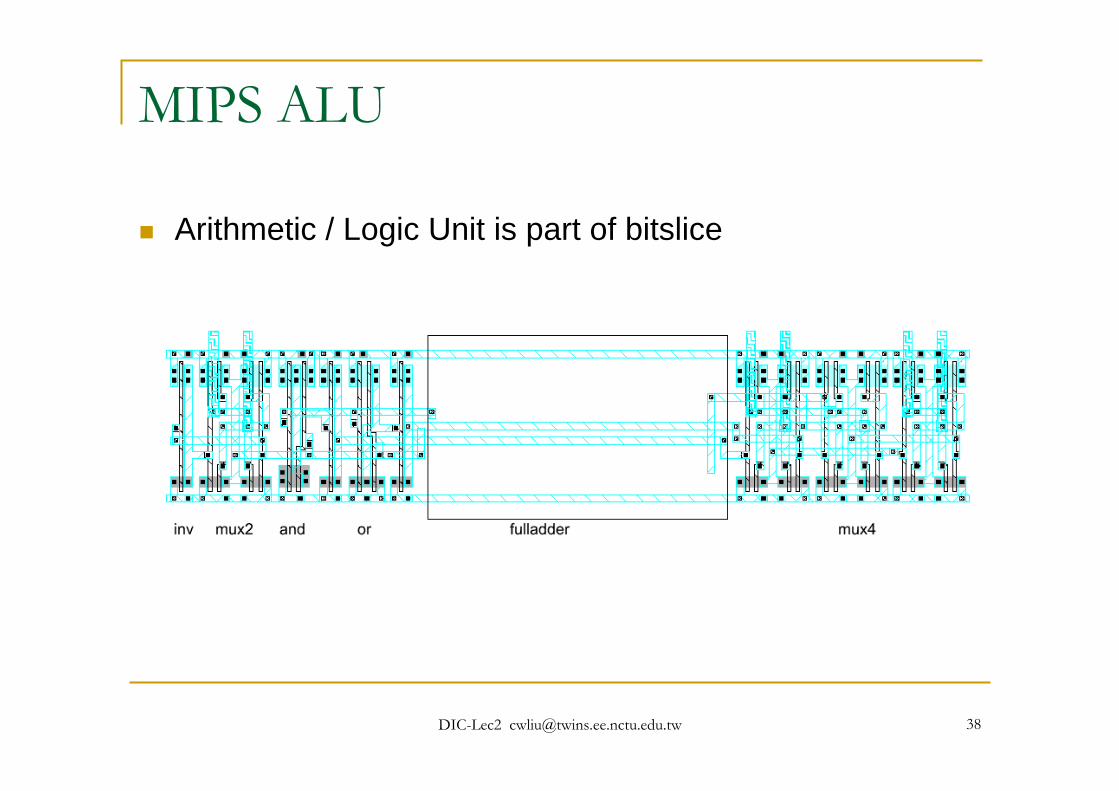
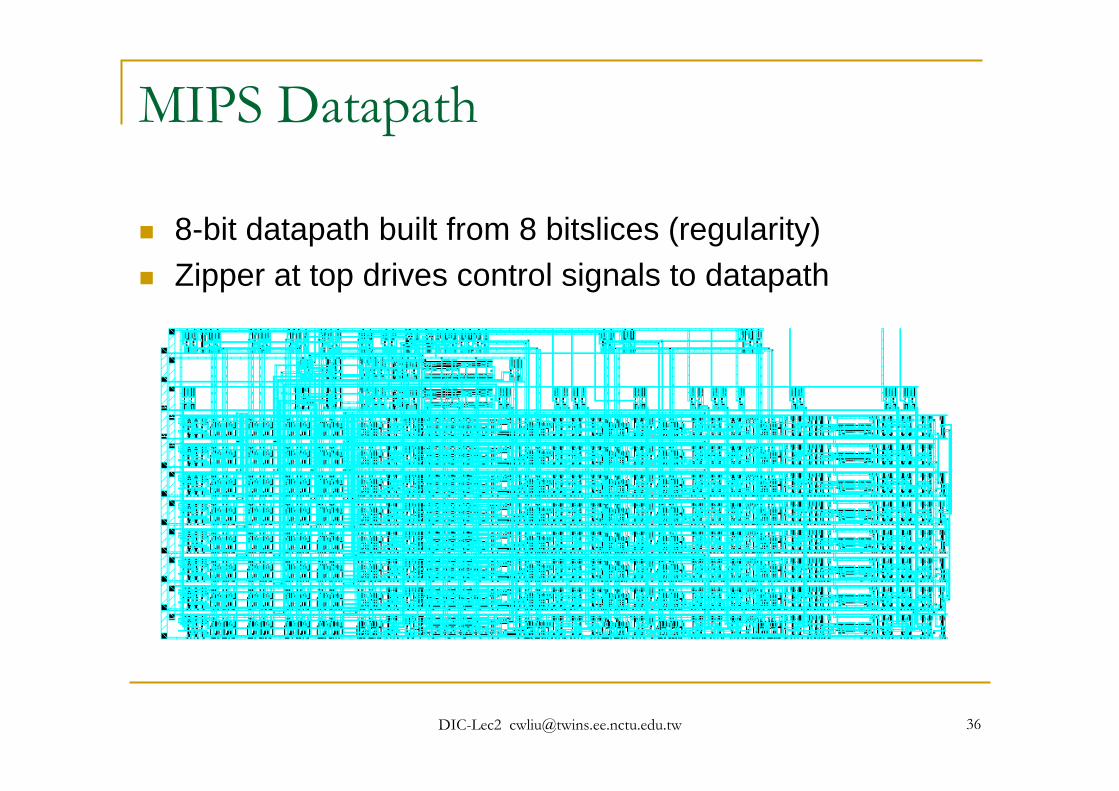
MIPS Datapath
8-bit datapath built from 8 bitslices (regularity)Zipper at top drives control signals to datapath
DIC-Lec2 [email protected] 37
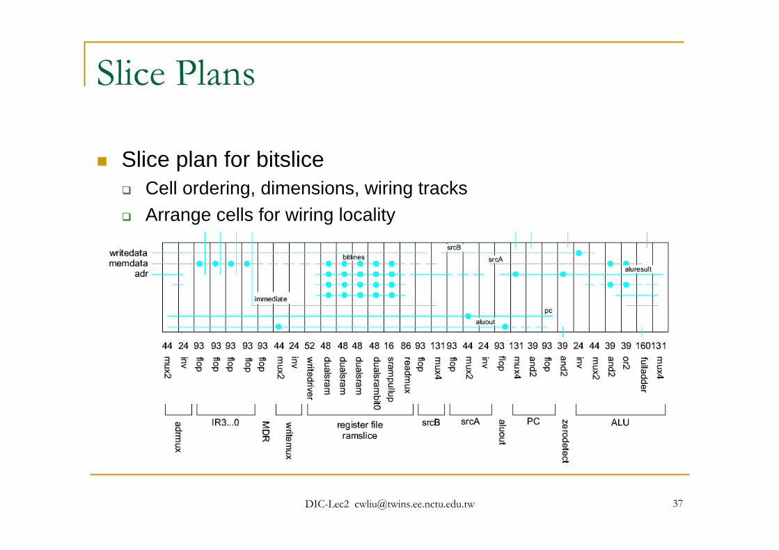
Slice Plans
Slice plan for bitsliceCell ordering, dimensions, wiring tracksArrange cells for wiring locality
DIC-Lec2 [email protected] 39
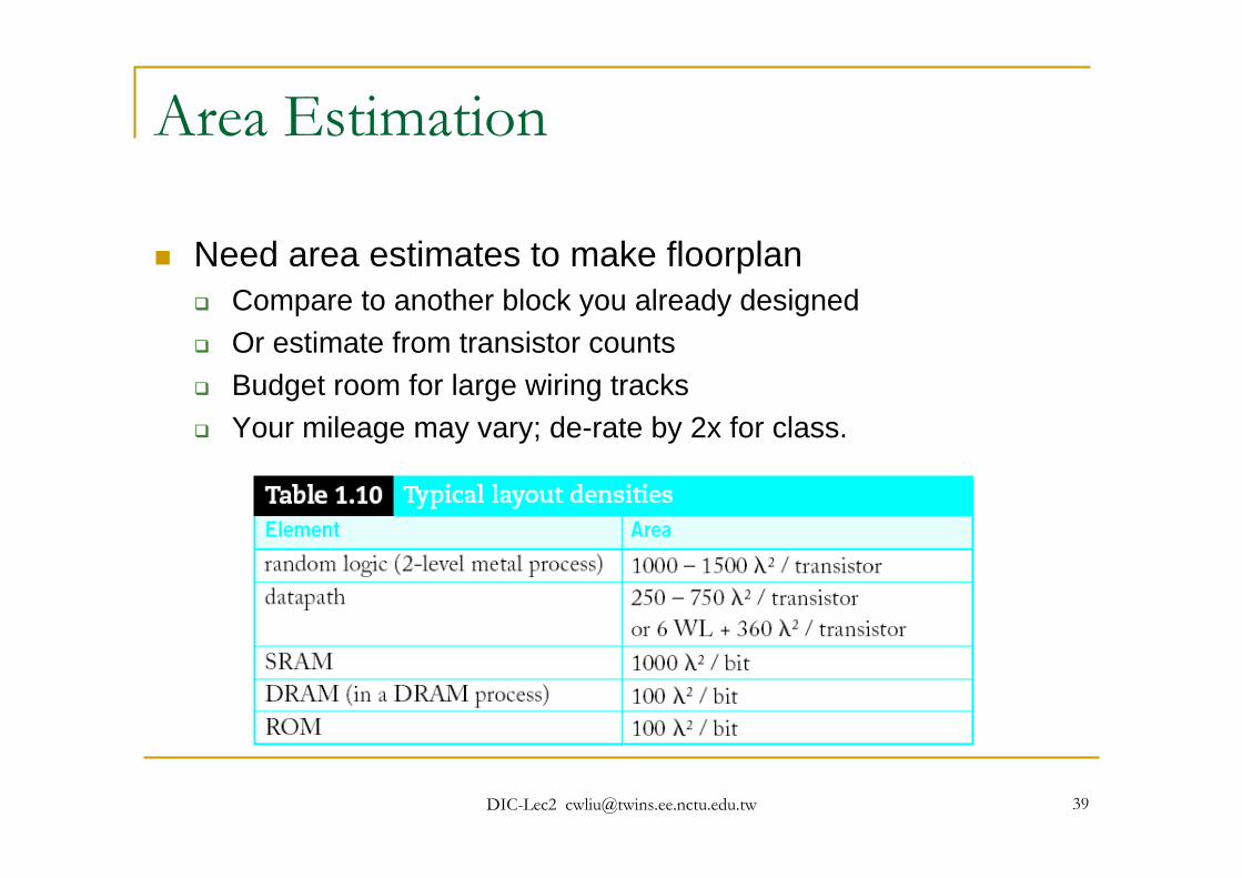
Area Estimation
Need area estimates to make floorplanCompare to another block you already designedOr estimate from transistor countsBudget room for large wiring tracksYour mileage may vary; de-rate by 2x for class.
DIC-Lec2 [email protected] 40
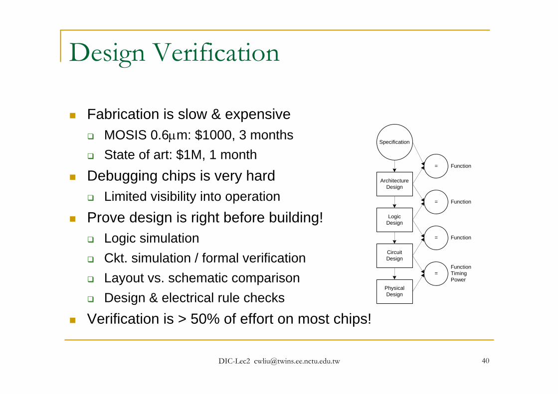
Design Verification
Fabrication is slow & expensiveMOSIS 0.6μm: $1000, 3 monthsState of art: $1M, 1 month
Debugging chips is very hardLimited visibility into operation
Prove design is right before building!Logic simulationCkt. simulation / formal verificationLayout vs. schematic comparisonDesign & electrical rule checks
Verification is > 50% of effort on most chips!
Specification
ArchitectureDesign
LogicDesign
CircuitDesign
PhysicalDesign
=
=
=
=
Function
Function
Function
FunctionTimingPower
DIC-Lec2 [email protected] 41
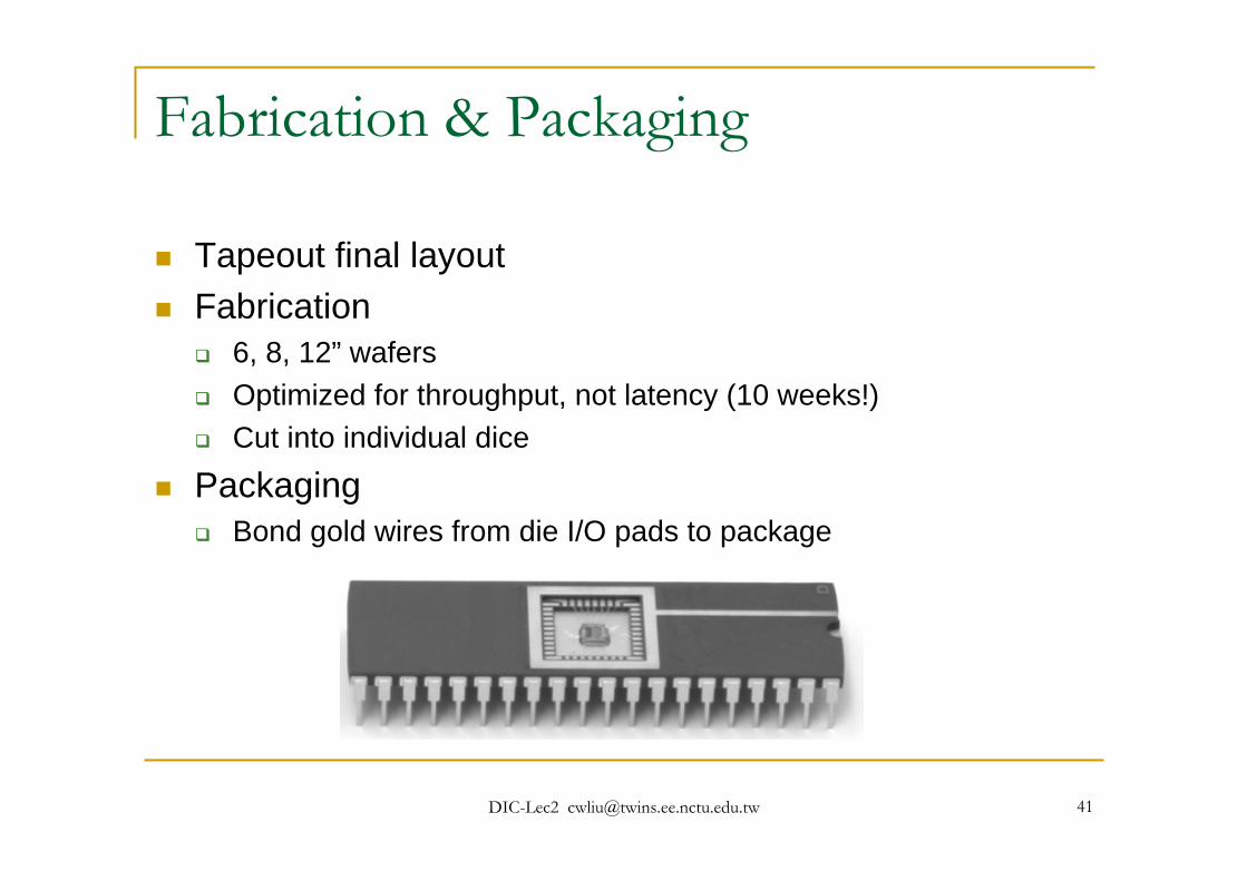
Fabrication & Packaging
Tapeout final layoutFabrication
6, 8, 12” wafersOptimized for throughput, not latency (10 weeks!)Cut into individual dice
PackagingBond gold wires from die I/O pads to package
DIC-Lec2 [email protected] 42
Testing
Test that chip operatesDesign errors
Manufacturing errors
A single dust particle or wafer defect kills a dieYields from 90% to < 10%
Depends on die size, maturity of process
Test each part before shipping to customer
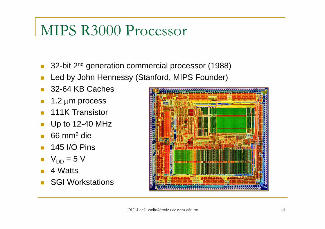
DIC-Lec2 [email protected] 44
MIPS R3000 Processor
32-bit 2nd generation commercial processor (1988)Led by John Hennessy (Stanford, MIPS Founder)32-64 KB Caches1.2 μm process111K TransistorUp to 12-40 MHz66 mm2 die145 I/O PinsVDD = 5 V4 WattsSGI Workstations