Embed Size (px)
Citation preview

EE 171 (Spring 2007)
1
EE 171
Digital Logic(Chapter 6)
University of California, Santa CruzMay 31, 2007
EE 171 (Spring 2007)
2
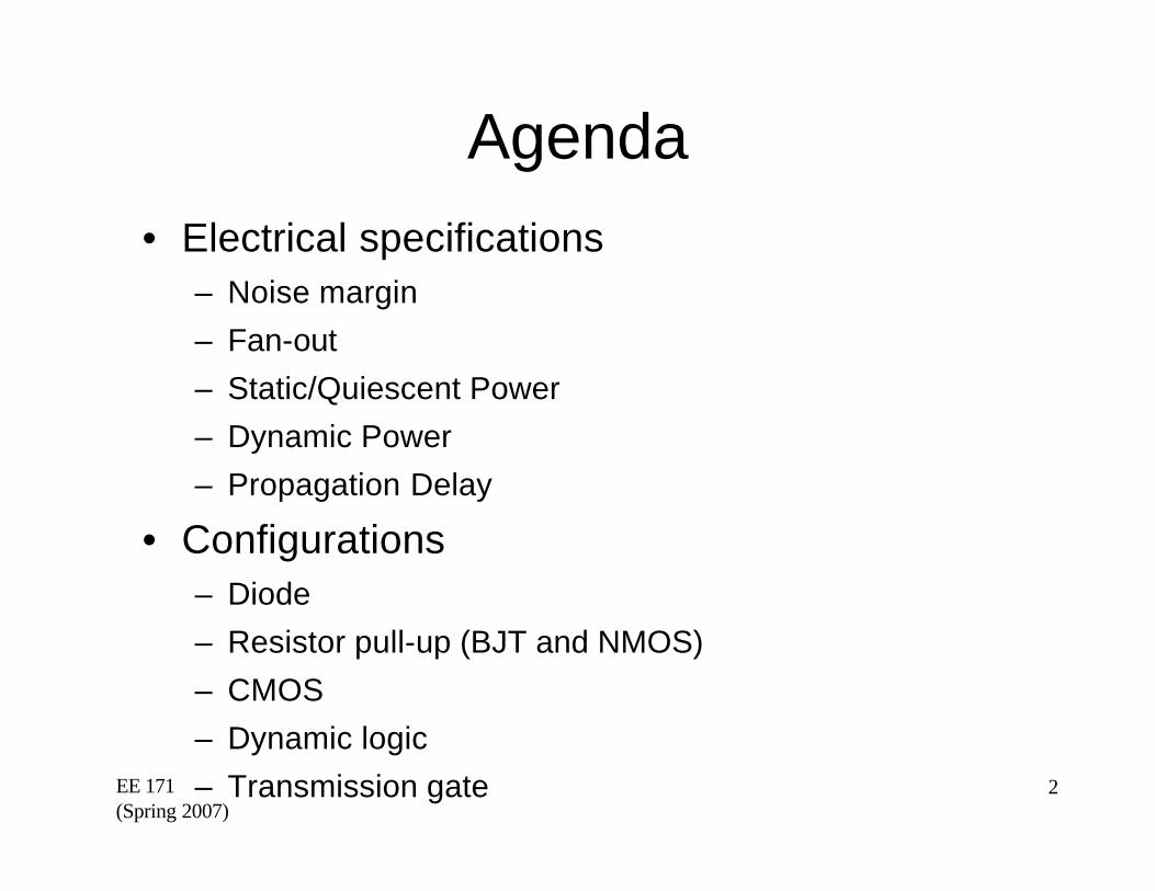
Agenda• Electrical specifications
– Noise margin
– Fan-out
– Static/Quiescent Power
– Dynamic Power
– Propagation Delay
• Configurations– Diode
– Resistor pull-up (BJT and NMOS)
– CMOS
– Dynamic logic
– Transmission gate

EE 171 (Spring 2007)
3Output voltage ranges for the 7400 ALS TTL logic family.
Logic Inverter• Digital signals are one of two possible states (on, off)
• Actual analog voltages get interpreted as either logic “1” logic “0” or “undefined”• Accounts for noise

EE 171 (Spring 2007)
4Voltage ranges for the 7400 ALS TTL logic
family operated from a +5-V supply.
Input and Output Voltage Ranges
VOH and VOL
VIH and VIL
• Logic circuits need to specify…• Worst case voltages produced at the output (VOH, VOL)• Minimum acceptable voltages on the input (VIH, VIL)• Need VOH > VIH and VIL > VOL

EE 171 (Spring 2007)
5
The inverter has a fan-out of 3 (i.e., the inverter drives 3 inputs).
Fan-Out
• Output can only drive a limited number of additional gates• Limited by the current that can
be supplied at the output• A certain input current is also
needed to ensure that switching time is reasonable
• Take the ratio• Minimum of IOH / IIH or IOL / IIL• For MOS logic, input I = 0
• Iout = CIN dv/dt• CIN depends on fan-out• Want short dv/dt
EE 171 (Spring 2007)
6
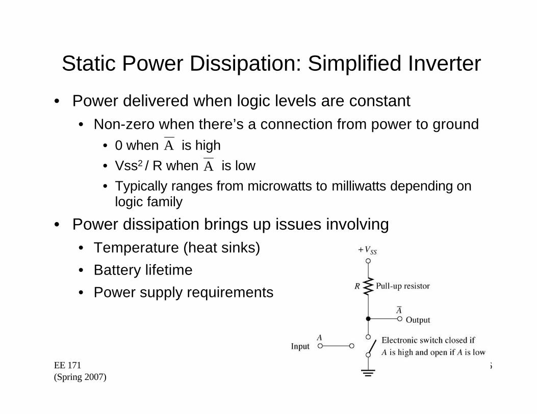
Static Power Dissipation: Simplified Inverter
• Power delivered when logic levels are constant• Non-zero when there’s a connection from power to ground
• 0 when is high• Vss2 / R when is low• Typically ranges from microwatts to milliwatts depending on
logic family
• Power dissipation brings up issues involving • Temperature (heat sinks)
• Battery lifetime
• Power supply requirements
AA

EE 171 (Spring 2007)
7
• Power needed to charge up/down capacitors when there is a change in state• Typical capacitance: fF to pF range
• Pdynamic = f Cin Vss2
• Energy stored in a capacitor: 1/2 CLVSS2 (units: Joules)
• All the stored energy in cap is dissipated in the switch in H to L transition (half-cycle)
• Power = Energy per unit time
Load capacitance causes dynamic power dissipation in a logic gate.
Dynamic Power Dissipation
Total Power Dissipation = Pstatic+Pdynamic

EE 171 (Spring 2007)
8
Transient Response of an Inverter
Propagation Delay, Rise and Fall Time
• Due to capacitance, logic levels do not go from high to low instantly• Rise/fall times: tr, tf
• Time it takes to go between the 10% and 90% points
• Propagation delay: tPHL, tPLH
• Time it takes for the output to transition, compared to the input
• Measured from 50% point
2tt
t PLHPHLpd
+=
EE 171 (Spring 2007)
9
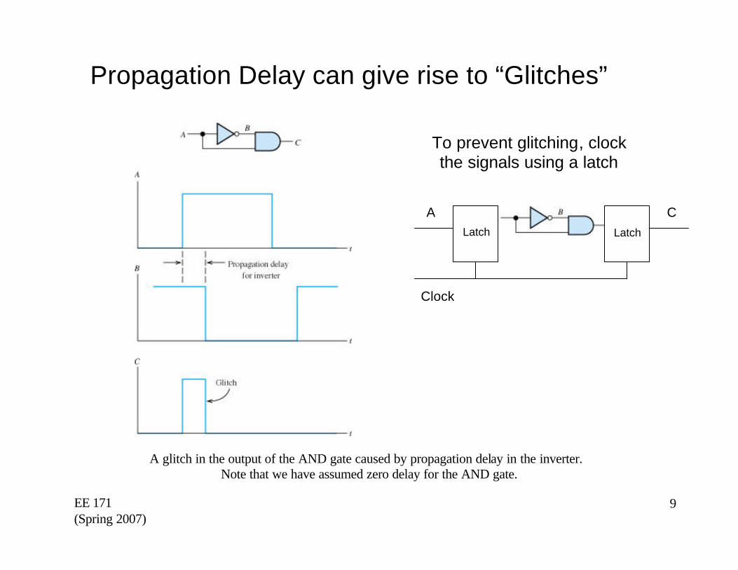
A glitch in the output of the AND gate caused by propagation delay in the inverter.Note that we have assumed zero delay for the AND gate.
Propagation Delay can give rise to “Glitches”
Latch Latch
Clock
To prevent glitching, clock the signals using a latch
Latch
A C
EE 171 (Spring 2007)
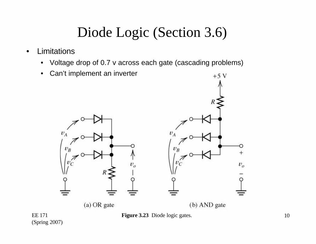
10Figure 3.23 Diode logic gates.
Diode Logic (Section 3.6)• Limitations
• Voltage drop of 0.7 v across each gate (cascading problems) • Can’t implement an inverter

EE 171 (Spring 2007)
11
BJT Digital Logic (Section 4.9)
• Early on, the BJT was used as logic switch in a logic family known as resistor-transistor logic (RTL)
• RTL inverter – If input = 0, BJT operates in cutoff. No current passes
through Rc and Vo equal to supply voltage

EE 171 (Spring 2007)
12
• For Vin > 0.7 v, the BJT turns on– Use input load-line to find base current
• Use a load-line on the output characteristics to find Vo– Minimum VOL = 0.2 v
Load-Line Analysis0ViRV BEbBin =−−
0ViRV CEcccc =−−
Note: assumes no loading
B
inBE
Bb R
VV
R1
i +−=
c
ccCE
cc R
VV
R1
i +−=
EE 171 (Spring 2007)
13
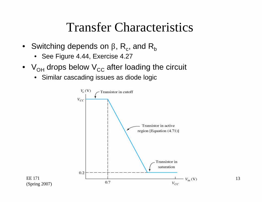
Transfer Characteristics• Switching depends on β, Rc, and Rb
• See Figure 4.44, Exercise 4.27
• VOH drops below VCC after loading the circuit• Similar cascading issues as diode logic
EE 171 (Spring 2007)
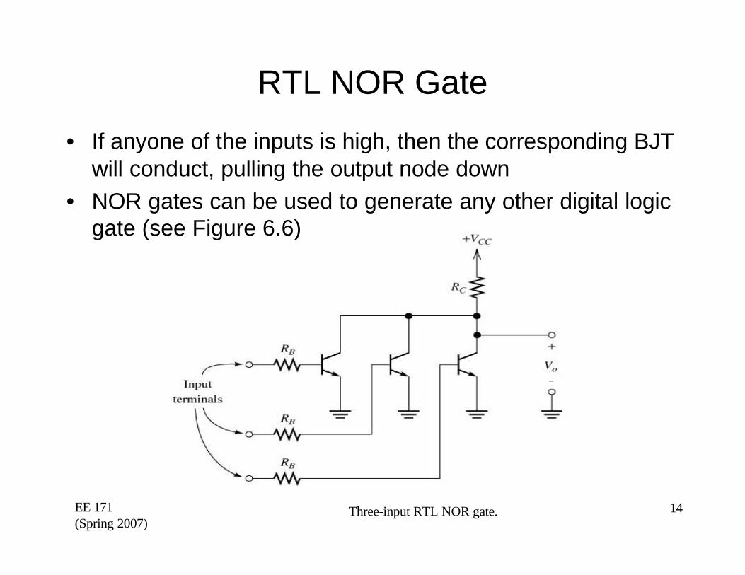
14Three-input RTL NOR gate.
RTL NOR Gate
• If anyone of the inputs is high, then the corresponding BJT will conduct, pulling the output node down
• NOR gates can be used to generate any other digital logic gate (see Figure 6.6)
–

EE 171 (Spring 2007)
15
90 kΩ
NMOS Inverter with Pull-Up Resistor
VOH = VDD
VOL = Ron / (RD+Ron) VDD
Want Ron << RD for good noise margin (VOL ~ 0)
• Similar to BJT RTL inverter• If VI = low, transistor is in cutoff (Vo = VDD)• If VI = high, transistor is in linear mode (Vo = VDS = low)
• Model transistor as a resistor and use voltage division
)VVV( TOGSDS −<<
−−=
2
VV)VV(
LW
KPI2
DStoGSdDS
DStoGSd V)VV(LW
KPI −=
)VV(LW
KP
1I
VR
toGSd
DSon
−==
Use large W/L ratio to keep Ron small

EE 171 (Spring 2007)
16
Loadline Analysis for the NMOS Inverter
VTO=1V
KP=50 µA/V2
λ=0
W/L=1/2
90 kΩ
D
DDDS
DD
DSDDDD
RV
VR1
i
0VRiV
+−=
=+−
VI = VGS = VDD = 5 v
Vo = low
VI = VGS = 0 vVo = VDS = 5 v

EE 171 (Spring 2007)
17
Inverter Transfer Characteristic
• Define VIL and VIH as points where the slope = –1

EE 171 (Spring 2007)
18
Low to High Output Transition
• VI = VDD to 0• NMOS turns off • Vo = low (VOH) to VDD
• Transient response resembles an RC circuit• Time constant = RDC
EE 171 (Spring 2007)
19
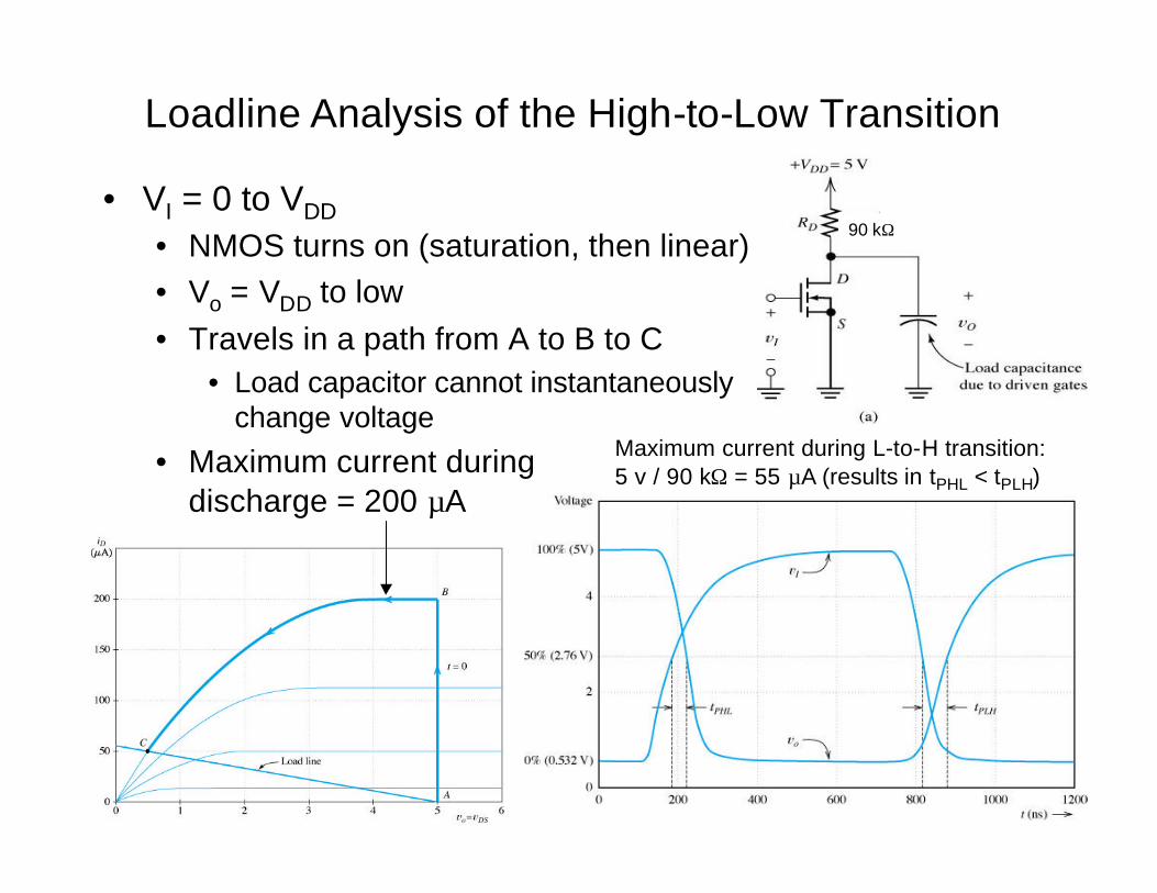
Loadline Analysis of the High-to-Low Transition
• VI = 0 to VDD
• NMOS turns on (saturation, then linear)• Vo = VDD to low• Travels in a path from A to B to C
• Load capacitor cannot instantaneously change voltage
• Maximum current during discharge = 200 µA
90 kΩ
Maximum current during L-to-H transition: 5 v / 90 kΩ = 55 µA (results in tPHL < tPLH)
EE 171 (Spring 2007)
20
90 kΩ
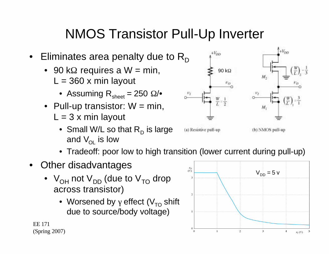
NMOS Transistor Pull-Up Inverter
• Eliminates area penalty due to RD
• 90 kΩ requires a W = min, L = 360 x min layout
• Assuming Rsheet = 250 Ω/•
• Pull-up transistor: W = min, L = 3 x min layout
• Small W/L so that RD is large and VOL is low
• Tradeoff: poor low to high transition (lower current during pull-up)
• Other disadvantages• VOH not VDD (due to VTO drop
across transistor)• Worsened by γ effect (VTO shift
due to source/body voltage)
VDD = 5 v

EE 171 (Spring 2007)
21
Other Pull-Up Configurations• Use a higher gate voltage on the pull-up transistor
• Eliminates VOH drop due to VTO
• Problem: requires 2 power supply voltages
• Use a depletion mode transistor as the pull-up• VTO < 0
EE 171 (Spring 2007)
22
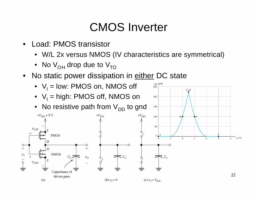
CMOS Inverter• Load: PMOS transistor
• W/L 2x versus NMOS (IV characteristics are symmetrical)• No VOH drop due to VTO
• No static power dissipation in either DC state• VI = low: PMOS on, NMOS off• VI = high: PMOS off, NMOS on• No resistive path from VDD to gnd

EE 171 (Spring 2007)
23
Graphical Analysis of a CMOS Inverter
DDIDDGSNGSP VVVVV −=−=
5VGSP −=
3VGSP −=
5.2VGSP −=
2VGSP −=
0VGSP =
DDDSPDSN VVV +=
Add VDD
VDSP
Transfer Characteristics
A: NMOS cutoff, PMOS offB: NMOS sat, PMOS linearC: NMOS sat, PMOS satD: NMOS sat, PMOS satE: NMOS: linear, PMOS satF: NMOS: off, PMOS cutoff

EE 171 (Spring 2007)
24
Propagation Delay: High to Low Transition
• Current used to discharge the capacitor is NMOS saturation• Assume λ = 0 and VDD/2 point is still in saturation• Similar equation for tPLH (use PMOS)
2TODDN
N
DDL
2TODD
N
N
DDL
2TOGS
LPHL
)VV(KPLW
VC
)VV(2
KPLW
2VC
)VV(2
KPLW
VCIQ
t−
=−
=−
∆==
x -
-
A: initial condition (Vin = low, Vout = high)B: Vin = high (capacitive load)C: Vout = 50% point

EE 171 (Spring 2007)
25
CMOS Logic Gates
Three-input NOR gate.
• 2-input NOR gate• If A or B is high, output is low• Output = high only if A and B are both low
• To maintain symmetry (transfer characteristic changes at VDD/2), different W/L ratios may be used• 2-input NOR: (W/L)p = 4 (W/L)n
• 2-input NAND: (W/L)p = (W/L)n
Goal: effective PMOS W/L = 2x effective NMOS W/L

EE 171 (Spring 2007)
26
Two Input NAND Gate
Transfer Function
A: sweep, B = VDD
A =VDD, B = sweep
A: sweep, B: sweep
Propagation Delay
Both PMOS transistorscharge up the load
Results depend on which Inputs are switching
EE 171 (Spring 2007)
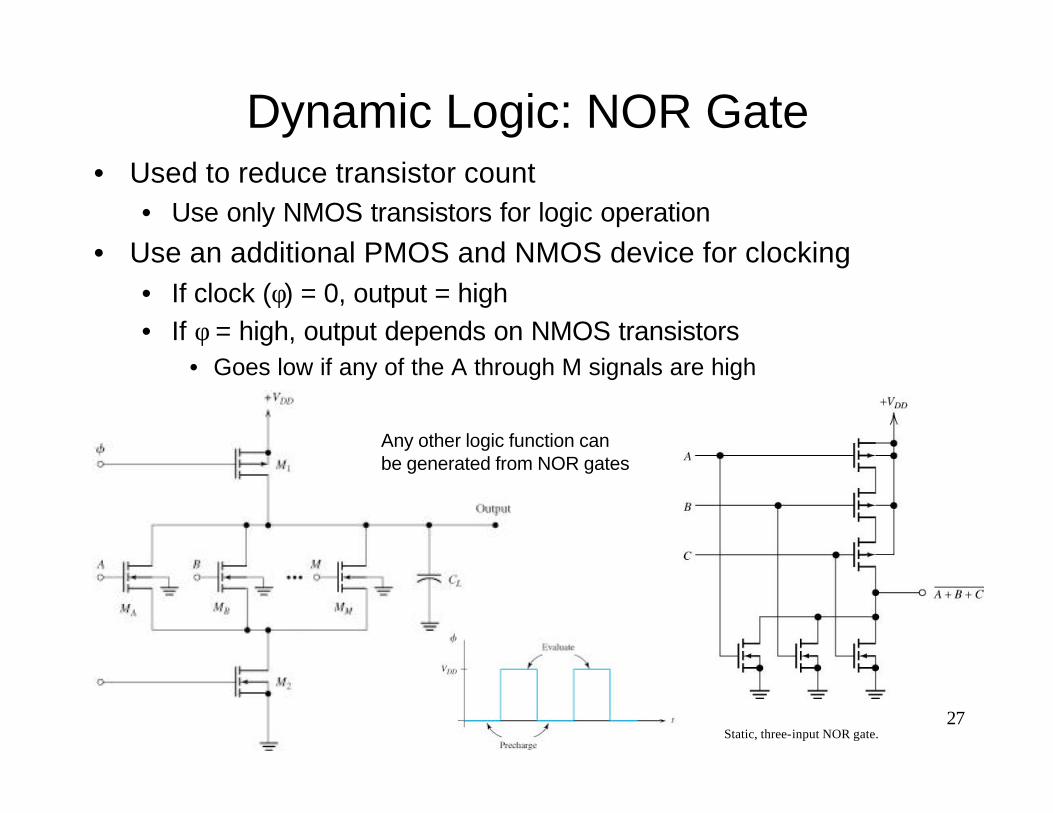
27
Dynamic Logic: NOR Gate• Used to reduce transistor count
• Use only NMOS transistors for logic operation
• Use an additional PMOS and NMOS device for clocking• If clock (φ) = 0, output = high• If φ = high, output depends on NMOS transistors
• Goes low if any of the A through M signals are high
Static, three-input NOR gate.
Any other logic function canbe generated from NOR gates

EE 171 (Spring 2007)
28
CMOS Analog Switch (Pass Gate)• Connects 1 to 2 if C is high
• Use 2 transistors to avoid VTO drop
• Can be used to implement logic
• Can be used as a switch