Embed Size (px)
Citation preview

Digital Logic Design ENEE 244-010x
Lecture 19
Announcements
• Homework 8 due on Monday, 11/23.
Agenda
• Last time: – Timing Considerations (6.3)
– Master-Slave Flip-Flops (6.4)
• This time: – Edge-Triggered Flip-Flops (6.5)
– Characteristic Equations (6.6)
– Registers (6.7)
– Counters (6.8-6.9)
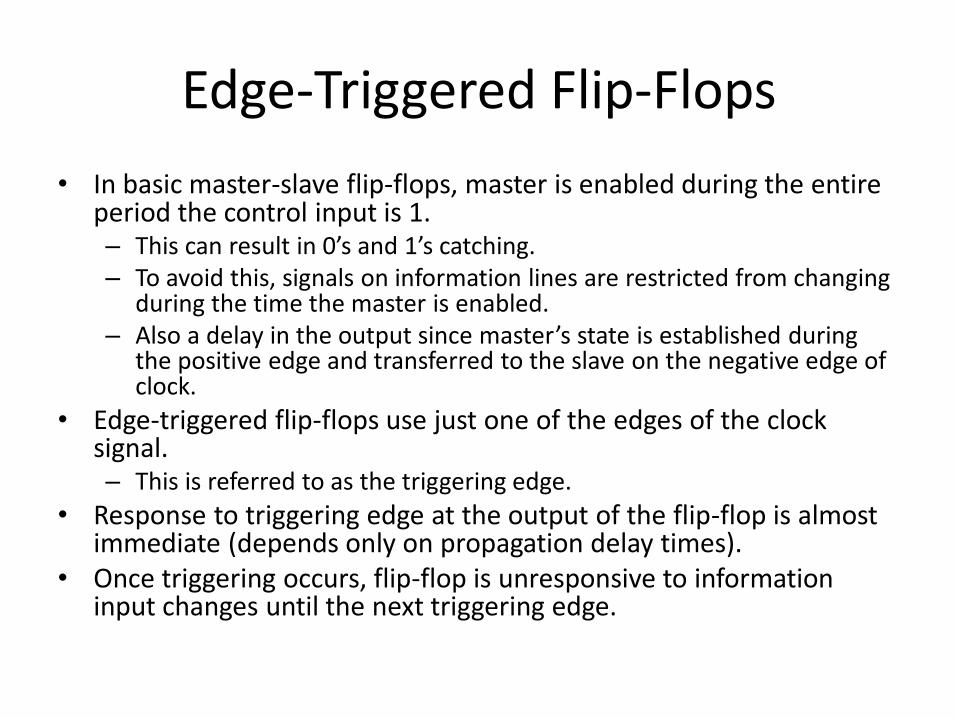
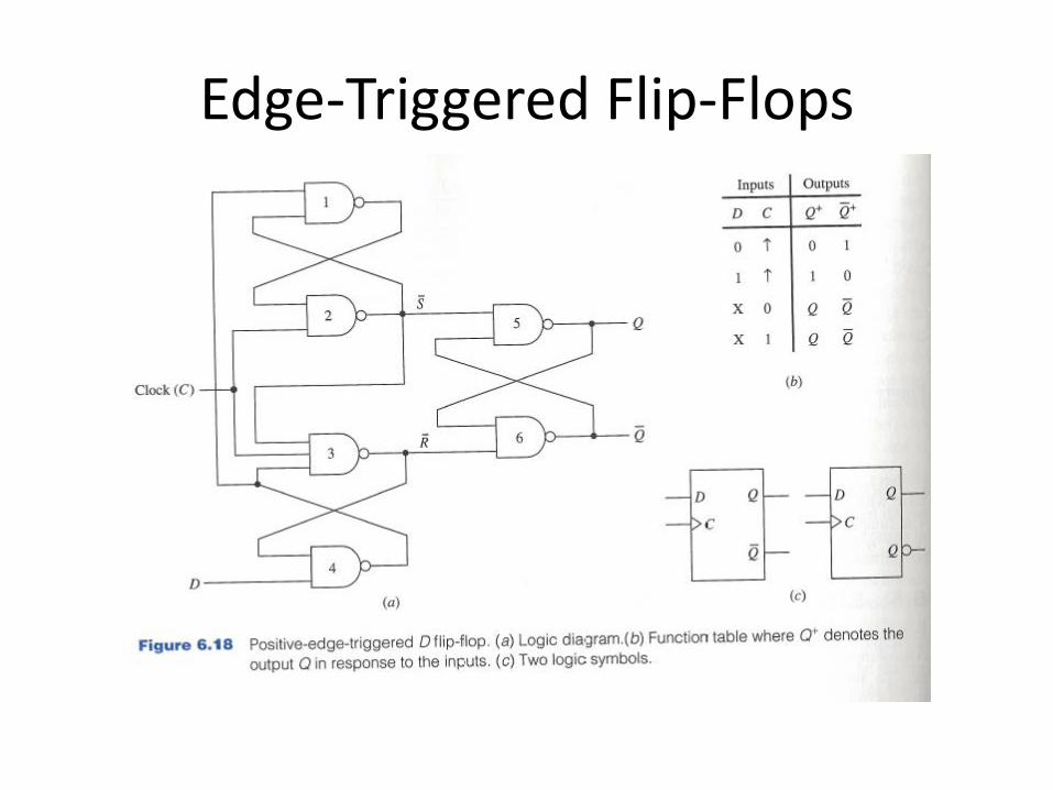
Edge-Triggered Flip-Flops
• In basic master-slave flip-flops, master is enabled during the entire period the control input is 1. – This can result in 0’s and 1’s catching. – To avoid this, signals on information lines are restricted from changing
during the time the master is enabled. – Also a delay in the output since master’s state is established during
the positive edge and transferred to the slave on the negative edge of clock.
• Edge-triggered flip-flops use just one of the edges of the clock signal. – This is referred to as the triggering edge.
• Response to triggering edge at the output of the flip-flop is almost immediate (depends only on propagation delay times).
• Once triggering occurs, flip-flop is unresponsive to information input changes until the next triggering edge.
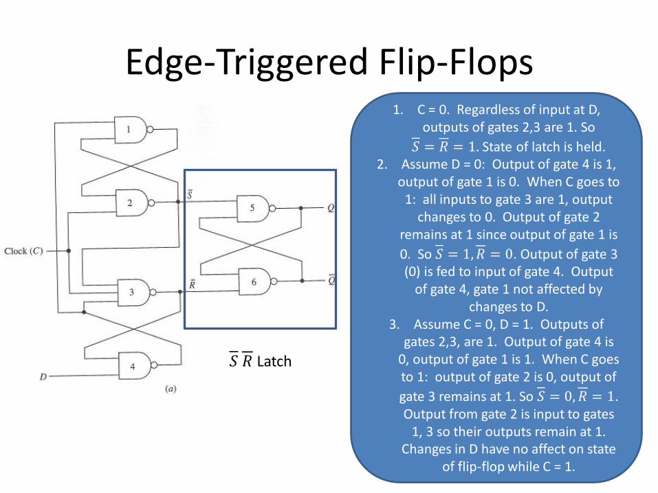
Edge-Triggered Flip-Flops 1. C = 0. Regardless of input at D,
outputs of gates 2,3 are 1. So
𝑆 = 𝑅 = 1. State of latch is held. 2. Assume D = 0: Output of gate 4 is 1,
output of gate 1 is 0. When C goes to 1: all inputs to gate 3 are 1, output
changes to 0. Output of gate 2 remains at 1 since output of gate 1 is
0. So 𝑆 = 1, 𝑅 = 0. Output of gate 3 (0) is fed to input of gate 4. Output
of gate 4, gate 1 not affected by changes to D.
3. Assume C = 0, D = 1. Outputs of gates 2,3, are 1. Output of gate 4 is
0, output of gate 1 is 1. When C goes to 1: output of gate 2 is 0, output of
gate 3 remains at 1. So 𝑆 = 0, 𝑅 = 1. Output from gate 2 is input to gates
1, 3 so their outputs remain at 1. Changes in D have no affect on state
of flip-flop while C = 1.
𝑆 𝑅 Latch
Edge-Triggered Flip-Flops

Timing Diagram
During setup and hold times 𝑡𝑠𝑢, 𝑡ℎ with respect to the triggering edge of the clock, D input must not change.
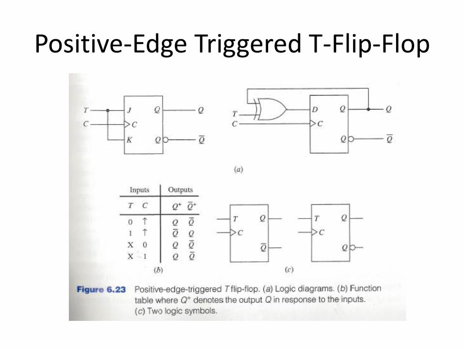
Positive-Edge Triggered T-Flip-Flop
Characteristic Equations
• Next state table: Shows the value of the next state of the flip-flop for each combination of values to the present state of the flip-flops and their information lines.
• The algebraic description of the next-state table of a flip-flop is called the characteristic equation of the flip-flop.
• Obtained by constructing the K-map for 𝑄+ in terms of the present state and information input variables.
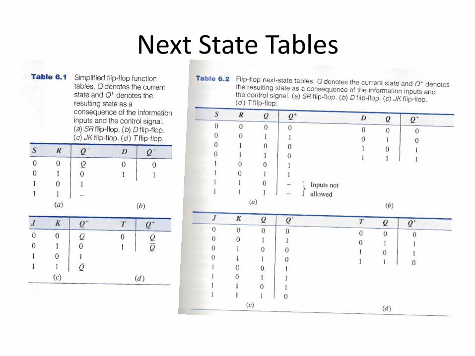
Next State Tables
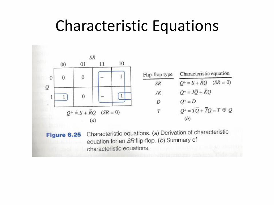
Characteristic Equations
Registers
• A collection of flip-flops taken as an entity. • Function: Hold information within a digital
system so that it is available to the logic elements during the computing process.
• Each combination of stored information is known as the state or content of the register.
• Shift register: Registers that are capable of moving information upon the occurrence of a clock-signal. – Unidirectional – bidirectional
Registers
• Two basic ways in which information can be entered/outputted – Parallel: All 0/1 symbols handled simultaneously. Require
as many lines as symbols being transferred.
– Serial: Involves the symbol-by-symbol availability of information in a time sequence.
• Four possible ways registers can transfer information: – Serial-in/serial-out
– Serial-in/parallel-out
– Parallel-in/parallel-out
– Parallel-in/serial-out
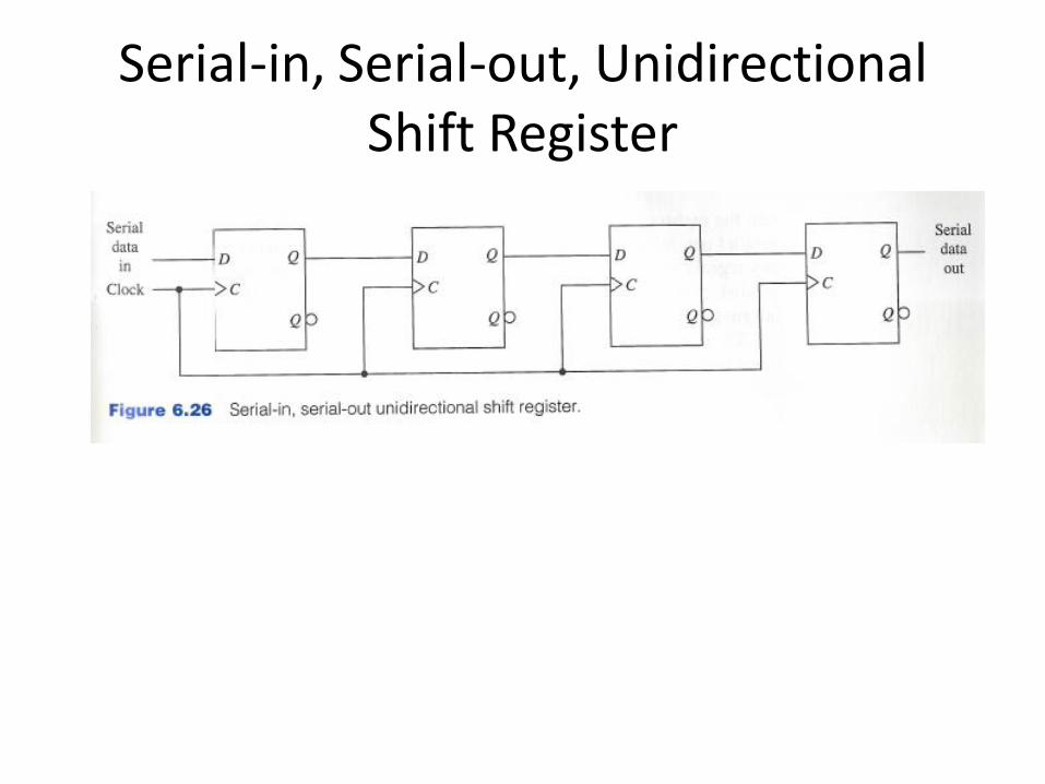
Serial-in, Serial-out, Unidirectional Shift Register
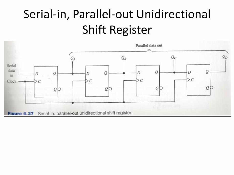
Serial-in, Parallel-out Unidirectional Shift Register
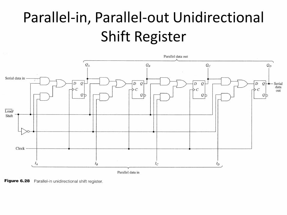
Parallel-in, Parallel-out Unidirectional Shift Register

Universal Shift Register
A bidirectional shift register. Capable of shifting contents either left or right depending upon the signals present on appropriate control input lines.
Universal shift register: Depending on the signal values on the select lines of the multiplexers, the register can retain its current state, shift right, shift left or be loaded in parallel. Each operation is
the result of a positive edge on the clock line.
Counters • An example of a register. • Primary purpose is to produce a specified output
pattern sequence. – Also called a pattern generator
• Each stored 0/1 combination is called the state of the counter.
• The total number of states is called its modulus. – If a counter has m distinct states then it is called a
mod-m counter.
• The order in which states appear is referred to as its counting sequence. – Depicted by a directed graph called a state diagram.
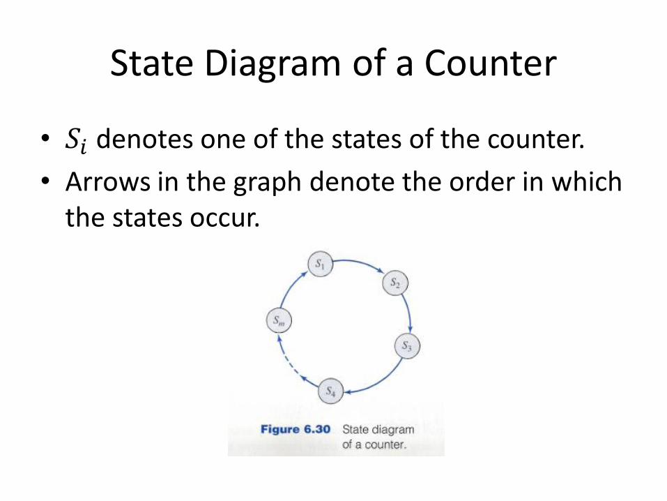
State Diagram of a Counter
• 𝑆𝑖 denotes one of the states of the counter.
• Arrows in the graph denote the order in which the states occur.
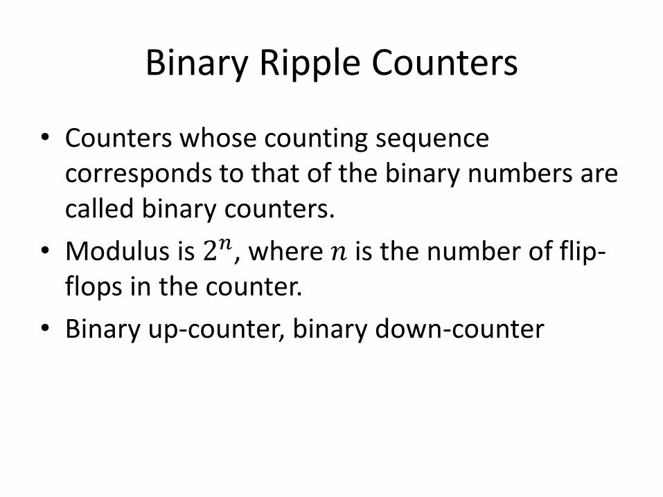
Binary Ripple Counters
• Counters whose counting sequence corresponds to that of the binary numbers are called binary counters.
• Modulus is 2𝑛, where 𝑛 is the number of flip-flops in the counter.
• Binary up-counter, binary down-counter

4-bit Binary Ripple Counter • Recall positive edge-triggered T-Flip-Flop.
– Each positive transition from logic-0 to logic-1 causes the flip-flop to toggle.

4-bit Binary Ripple Counter

4-bit Binary Ripple Counter • Known as a ripple counter since a change in the state of the
𝑄𝑖−1flip-flop is used to toggle the 𝑄𝑖 flip-flop. – The effect of a count pulse must ripple through the counter. – Ripple counters also referred to as asynchronous counters.
• Propagation Delay – There is a propagation delay between the input and output of a
flip-flop. – Rippling behavior affects the overall time delay between the
occurrence of a count pulse and when the stabilized count appears at the output terminals.
– Worst Case? – Going from 111 ⋯ 111 to 000 ⋯ 000 since toggle signals must
propagate through the entire length of the counter.
– For n-stage binary ripple counter, the worst case time is 𝑛 ⋅ 𝑡𝑝𝑑, where 𝑡𝑝𝑑 is the propagation delay time associated with each flip-flop.

Synchronous Binary Counters
• All flip-flops change simultaneously after the appropriate propagation delay associated with a single flip-flop.
• Count pulses are applied directly to the control inputs, C, of all the clocked flip-flops.
– All flip-flops change simultaneously after the appropriate propagation delay associated with a single flip-flop.
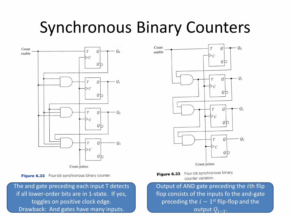
Synchronous Binary Counters
The and gate preceding each input T detects if all lower-order bits are in 1-state. If yes,
toggles on positive clock edge. Drawback: And gates have many inputs.
Output of AND gate preceding the 𝑖th flip flop consists of the inputs fo the and-gate
preceding the 𝑖 − 1st flip-flop and the output 𝑄𝑖−1.

Mod-m Counter
• Use a mod-2𝑛 counter as a mod-𝑚 counter. – Load an initial binary number prior to the counting
operation.
– Counter structure is modified to allow for parallel loading.
– JK flip-flops are used instead of T flip-flops.
• Two enable signals: – Load enable: Allows parallel loading of data inputs
𝐷0, 𝐷1, 𝐷2, 𝐷3
– Count enable: allows for counting.
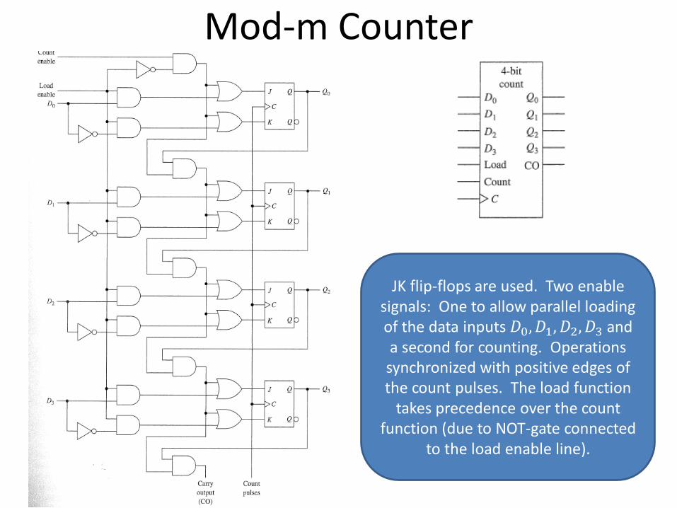
Mod-m Counter
JK flip-flops are used. Two enable signals: One to allow parallel loading of the data inputs 𝐷0, 𝐷1, 𝐷2, 𝐷3 and a second for counting. Operations synchronized with positive edges of the count pulses. The load function
takes precedence over the count function (due to NOT-gate connected
to the load enable line).

Mod-10 Counter

![Journal of Experimental Zoology Part a Ecological Genetics and Physiology Volume 275 Issue 2-3 1996 [Doi 10.1002%2F%28sici%291097-010x%2819960601%2F15%29275%3A2%2F3%3C217%3A%3Aaid-Jez13%3E3.0.Co%3B2-g]](https://img.pdfslide.net/doc/110x75/577cdf1c1a28ab9e78b08029/journal-of-experimental-zoology-part-a-ecological-genetics-and-physiology-volume.jpg)