Embed Size (px)
Citation preview
Digital Signal Processing Hardware
for a Fast Fourier Transform Radio Telescopeby ARCHrES
Jonathan L. Losh
S.B., Electrical Engineering M.I.T., 2011
Submitted to the Department of Electrical Engineering
and Computer Science
in Partial Fulfillment of the Requirements for the Degree of
Master of Engineering in Electrical Engineering and Computer Science
at the Massachusetts Institute of Technology
May 2012
Copyright 2012 Jonathan L Losh. All rights reserved.
The author hereby grants to M.I.T. permission to reproduce and to distribute publicly paperand electronic copies of this thesis document in whole and in part in any medium now known
or hereafter created.
Author:Department of Electrical Engineering and Computer Science
May 21, 2012
Certified by:Max Tegmark, Department of Physics
May 21, 2012
Accepted by:.Prof. Denmiis M Freeman, Chairman, Masters of Engineering Thesis Commitee
May 21, 2012
1
Digital Signal Processing Hardware for a Fast Fourier Transform Radio Telescope
by
Jonathan L. Losh
Submitted to the Department of Electrical Engineering
and Computer Science
May 21, 2012
in Partial Fulfillment of the Requirements for the Degree of
Master of Engineering in Electrical Engineering and Computer Science
at the Massachusetts Institute of Technology
Abstract21-cm tomography is a devoloping technique for measuring the Epoch of Reioniza-
tion in the universe's history. The nature of the signal measured in 21-cm tomography
is such that a new kind of radio telescope is needed: one that scales well into very large
numbers of antennas. The Omniscope, a Fast Fourier Transform telescope, is exactly
such a telescope. I detail the implementation of the digital signal processing backend
of a 32-channel interferometer designed to help characterize the non-digital parts of
the system, starting at the point analog signal enters the FPGA and ending when it is
written to a file on a computer. I also describe the accompanying subsystems, my im-
plementation of a scaled-up, 64 channel design, and lay out a framework for expanding
to 256 channels.

Acknowledgements
I would like to thank everyone I've worked with these past two and a half
years: Nevada Sanchez and Jack Hickish for mentoring me and putting up
with my incessant questions. Eben Kunz for his down-to-earth advice on
all matters. Ashley Perko and Hrant Gharibyan for testing my early de-
signs. Andy Lutomirski for answering the most impossibly obscure queries.
Adrian Liu for teaching me the actual astrophysics that this machine is
calculating. Kevin Zheng for helping me debug extremely strange digital
problems. loana Zelko and Devon Rosner for being diligent pupils. Jeff
Zheng for his invaluable and diligent help in finding and fixing countless
bugs in my design. Finally, Max Tegmark for getting me to work on this
project, without which I would have never learned, kicking and screaming,
an impressive set of engineering tools.
On a more personal note, I'd like to thank all of my friends, who have
made MIT the incredible experience it has been. I'd also like to thank my
parents, whom this thesis is dedicated to, for working so hard to give me
the opportunity to grow so much.


Contents
List of Figures
List of Tables
1 Introduction
1.1 32-channel interferometer . . .
1.2 Programmable DSP Hardware.
1.3 CASPER Hardware
1.4 A Roadmap for This Thesis
2 F-Engine
2.1 Purpose .............
2.2 Overview ............
2.3 ADC ...............
2.4 Windowing .............
2.5 FFT ..................
2.6 Shifter/Truncator .........
2.7 Spectrum Divider .........
2.8 Transposer ...........
2.9 10-Gigabit Ethernet . . . . . .
2.10 Monitoring BRAM . . . . . . .
3 X-Engine
3.1 Purpose . . . . . . .
3.2 Overview . . . . . .
3.3 10Gbe Receiving System .
vii
ix
1
. 2
. 3
. 4
. 4
7
7
7
7
9
10
12
14
15
18
19
21
21
21
22
.
. . . . . . . . . . . . . . . . . . . . . . . . . . . . .
. . . . . . . . . . . . . . . . . . . . . . . . . . . . .
CONTENTS
. . . . . . . . . . . . . . . . . . . 24
. . . . . . . . . . . . . . . . . . . 24
3.4 Cross-correlator ...............
3.5 Vector Accumulator ...........
4 Transmitting and Receiving Software
4.1 Purpose
4.2
4.3
4.4
Overview .......
Transmitting Software
Receiving Software . .
5 ROACH Viewer
5.1 Purpose . . . . .
5.2 Overview . . . .
6 Swapper
6.1 Purpose . . . . .
6.2 Overview . . . .
6.3 Digital swapping
6.4 Analog swapping
6.5 Zeroing ......
7 64-Channel F-engine
7.1 Purpose ............
7.2 Overview ...........
7.3 Changes in F-engine . . . . .
7.4 Changes in X-engine . . . . .
7.5 Changes in receiving software
8 Quad F-engine Roadmap
8.1 Purpose ............
8.2 Overview ...........
8.3 Clocking ...............
8.4 X-engine changes ........
27
27
27
27
29
35
. ... . 35
.... . 35
37
. . . . . . . . . . . . . . 37
. . . . . . . . . . . . . . 37
. . . . . . . . . . . . . . 38
. . . . . . . . . . . . . . 38
. . . . . . . . . . . . . . 38
43
43
43
44
45
45
47
47
47
48
49
. . . . . . . . . . . . . . . . . . . . . . . . . 52
. . . . . . . . . . . . . . . . . . . . . . .
. . . . . . . . . . . . . . . . . . . . . . .
8.5 Receiving software changes
CONTENTS
9 Conclusion 53
9.1 Summary of Results ............................ . 53
9.2 Future Work ....... ................ ............... .. 53
Bibliography 55

CONTENTS
List of Figures
1.1 Timeline of the universe . . . . . . . . . . . . . . . . . . . . .
1.2 Overview of the 32-channel correlator . . . . . . . . . . . . .
1.3 System diagram for CASPER's ROACH board . . . . . . . .
2.2
2.3
2.4
2.5
2.6
2.7
2.8
2.9
ADC data format . . . . . . . . . . . . . . . . . . . . . . . . . . . . . . . 8
4-tap polyphase filtering calculation for FFT length 256 . . . . . . . . . 10
Modified FIR filter . . . . . . . . . . . . . . . . . . . . . . . . . . . . . . 11
FFT data format . . . . . . . . . . . . . . . . . . . . . . . . . . . . . . . 12
Diagram of shifter/truncator . . . . . . . . . . . . . . . . . . . . . . . . 13
Dataflow for spectrum divider module. . . . . . . . . . . . . . . . . . . . 14
Data order out of the FFT . . . . . . . . . . . . . . . . . . . . . . . . . 15
Data order correlator expects . . . . . . . . . . . . . . . . . . . . . . . . 16
3.1 Block diagram of X-engine . . . . . . . . . . . . . . . . . . . . . . . . . .
3.2 10gbe Buffer . . . . . . . . . . . . . . . . . . . . . . . . . . . . . . . . .
3.3 Vector accumulator for vector length 3 . . . . . . . . . . . . . . . . . . .
4.1 Block diagram of software chain . . . . . . . . . . . . . . . . . . . . . . .
4.2 Time-multiplexed UDP sending for 2 X-engines . . . . . . . . . . . . . .
4.3 Receiving software reconstruction of accumulation . . . . . . . . . . . .
4.4 Multi-process X-engine receiving software for 2 X-engine case . . . . . .
5.1 Screenshot of the ROACH Viewer . . . . . . . . . . . . . . . . . . . . . .
6.1 Analog hardware . . . . . . . . . . . . . . . . . . . . . . . . . . . . . . .
6.2 Signals for analog hardware . . . . . . . . . . . . . . . . . . . . . . . . .
1
3
5
21
23
25
28
30
31
32
36
39
40
LIST OF FIGURES
6.3 Transient behavior of ZMAS-1 switch ...... ................... 41
7.1 System for halving time data ........................ 44
8.1 Clock distribution system . . . . . . . . . . . . . . . . . . . . . . . . . . 48
8.2 Block diagram for X-engine receiving from 4 F-engines . . . . . . . . . . 50
8.3 Multi-10gbe buffer for two 10gbe channels . . . . . . . . . . . . . . . . . 51

List of Tables
2.1 BRAM usage for major subsystems...................... 17

LIST OF TABLES

1
Introduction
Dark EnergyAccelerated Expansion
Afterglow LightPattern D ark Ages Development of
380.000 yrs. Galaxies, Planets, etc. 7
Inflation,-
9 WMIAP
QuantumFluctuations-
1 st Starsabout 400 million yrs.
Big Bang Expansion
13.7 billion years
Figure 1.1: Timeline of the universe - Time proceeds from the Big Bang at the left to
the present day at the right. The Omiscope aims to measure the "Dark Ages," starting
at around 400,000 years after the Big Bang and continuing for about 200 million years.
The goal of the Omniscope is to measure the early universe. Because electromag-
netic radiation travels at a finite speed, we can actually look at electromagnetic (EM)
waves emitted from back then to see what was going on. An era of great interest to
1. INTRODUCTION
us is the Epoch of Reionization, a period of time when the universe, which was com-
prised of mostly neutral hydrogen up until this point, started to undergo a process in
which some hydrogen became reionized. Neutral hydrogen emits a very specific kind of
EM radiation with a wavelength of 21-cm. By capturing this signal, we can see where
neutral hydrogen existed and where it didn't. By doing so, we can gather information
about how first stars formed. Furthermore, since the universe has expanded since these
EM waves have been omitted, the wavelength of the 21-cm photons expands as well,
allowing us to figure out when a photon was emitted based on how much its wavelength
has expanded. Thus, we can make maps not only varying in space, but also in time.
All of this wonderful potential brings up some serious obstacles. First of all, since
the signal is from so far away, it is very faint. To have a chance at measuring it
in the face of noise and other EM sources radiating much more intensely, we need a
very sensitive telescope. In the world of radio interferometry, higher sensitivity means
more antennas. In a traditional radio interferometer, the cost of adding more antennas
goes asymptotically as O(N 2), where N is the number of antennas. This is because
a normal interferometer needs to take the cross-correlation for each pair of antennas
it has, so for large number of antennas, the cost is dominated by needing to calcu-
late this quadratically growing number of pairs. The Omniscope's design avoids this
problem by arranging its antennas in regular grids and taking a spatial FFT instead of
cross-correlating. Thus, the Omniscope's cost of adding antennas goes as O(Nlog(N)),
allowing it to scale into the millions of antennas at a reasonable cost. A more thorough
discussion of Omniscopes can be found in the original Omniscope papers (1) (2).
1.1 32-channel interferometer
My thesis project centered around the construction of the digital signal processing
chain for an interferometer capable of taking in data from 32 ADC channels, Fourier
transforming that data into the frequency domain, taking the cross-correlations of each
pair of channels, and then time-averaging these cross-correlations. This may sound
like the kind of normal interferometer that the Omniscope is trying to replace, and
that's because it is. The goal of this iteration of the design is to fully characterize
all of the other unknowns in our system, such as the effect of the analog hardware
in between the antennas and the ADC, how well the calibration software works that
1.2 Programmable DSP Hardware
processes the data that comes out, and anything else that is not the core processing of
a normal interferometer. Once those effects are known, we can simply reconfigure the
cross-correlation stage to be a spatial FFT, and we have an Omniscope.
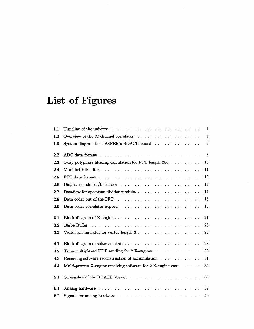
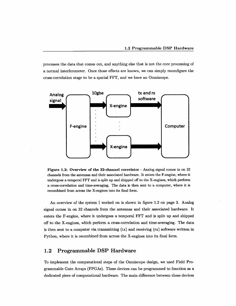
Figure 1.2: Overview of the 32-channel correlator - Analog signal comes in on 32
channels from the antennas and their associated hardware. It enters the F-engine, where it
undergoes a temporal FFT and is split up and shipped off to the X-engines, which perform
a cross-correlation and time-averaging. The data is then sent to a computer, where it is
recombined from across the X-engines into its final form.
An overview of the system I worked on is shown in figure 1.2 on page 3. Analog
signal comes in on 32 channels from the antennas and their associated hardware. It
enters the F-engine, where it undergoes a temporal FFT and is split up and shipped
off to the X-engines, which perform a cross-correlation and time-averaging. The data
is then sent to a computer via transmitting (tx) and receiving (rx) software written in
Python, where it is recombined from across the X-engines into its final form.
1.2 Programmable DSP Hardware
To implement the computational steps of the Omniscope design, we used Field Pro-
grammable Gate Arrays (FPGAs). These devices can be programmed to function as a
dedicated piece of computational hardware. The main difference between these devices
1. INTRODUCTION
and ordinary computers is that the computations in an FPGA can be implemented at
the gate level, rather than at the software level. This allows us to implement dedicated
digital signal processing hardware at significantly higher speeds than a software DSP,
not only because the computations can be pipelined at the logic level, but because they
can readily be made parallel.
Upon digitizing the signals coming from each antenna, we will have an FPGA that
will perform the F-Engine computation. This data will then be sent over a 10Gb
Ethernet link, where it will be received by the appropriate X-Engine. The X-Engine
will also be implemented using FPGAs.
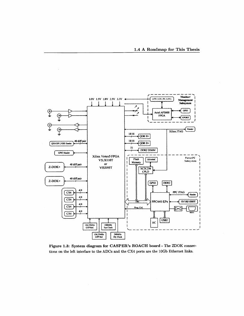
1.3 CASPER Hardware
In the early stages of the Omniscope project, we used hardware designed by the
CASPER group at Berkeley. This group is dedicated to building open-source pro-
grammable hardware specifically for applications in astronomy. One of their newer
devices is called the ROACH. It contains a Xilinx Virtex 5 FPGA that is programmed
and controlled by a PowerPC processor running a Linux kernel. It also features a
number of useful peripheral connections such as 10Gb Ethernet links and ports for
connecting high performance ADCs. A system diagram of the ROACH is shown in
figure 1.3.
The main benefit of using CASPER hardware is that it eliminates a large part of
the design process for radio telescopes: namely, the amount of time it takes to design
and build custom hardware. Also, along with their hardware comes a large open-source
library of FPGA programming structures such as polyphase filter bank FIR filters and
fast Fourier transform blocks, which saves us the trouble of having to re-invent the
wheel, i.e., commonly used signal processing structures.
1.4 A Roadmap for This Thesis
This thesis is aimed at giving readers an understanding of how the system works so
that one could build upon the system to scale it up to process even more channels. To
this end, it first covers the details of how I implemented the various subsystems of the
32-channel interferometer. In chapter 2, I cover the F-engine, chapter 3, the X-engine,
1.4 A Roadmap for This Thesis
ATX IIIV. sV.33V I Monitr/MAsnemt
I I ---Z
Figure 1.3: System diagram for CASPER's ROACH board - The ZDOK connec-
tions on the left interface to the ADCs and the CX4 ports are the 10Gb Ethernet links.

1. INTRODUCTION
and chapter 4, the transmitting and receiving software. These systems were designed
in collaboration with Nevada Sanchez and Kevin Zheng, and heavily drew inspiration
from a previous design Jack Hickish of Oxford had made for the group, who in turn
adapted it from a CASPER design spearheaded by Jason Manley. Verification that the
system produced valid output would not have been possible without the efforts of Jeff
Zheng, who throughly tested the system end-to-end to discover any processing errors.
Two ancillary systems run alongside the main processing: the ROACH viewer and the
swapper. Chapter 5 discusses the ROACH viewer, developed with the help of Nevada
Sanchez and Ioana Zelko, which allows us to view data inside the F-engine in real time.
Chapter 6 covers the swapper, a system designed to suppress cross-talk between the
ADC channels. It was developed alongside Nevada, Eben Kunz, and Hrant Gharyibyan.
After covering the 32-channel design, I go into detail on how I expanded its capabilities
to process 64 channels in chapter 7, covering the bottlenecks in the system that forced
us to make tradeoffs and each change made to the subsystems. Finally, I lay out a
sketch of the changes needed to make a design using four F-engines rather than one in
chapter 8.
2
F-Engine
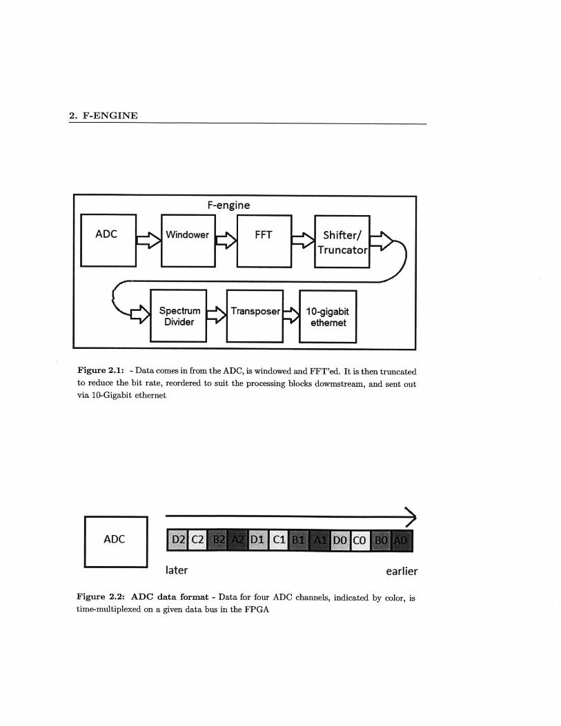
2.1 Purpose
The first step of the digital signal processing chain involves performing a Fourier trans-
form on the data to represent it in the frequency domain. Because the correlator block
downstream in the X-engine wants data in a very different order than it naturally comes
out, the data must then be rearranged. To move the data from the F-engine FPGA to
the X-engine FPGA, it is shipped off via 10-Gigabit ethernet.
2.2 Overview
Data first comes in via the ADC. Before we take the Fourier transform, we apply a
window to the data to minimize the phenomenon known as spectral leakage, in which
the finite time window causes some frequency components to "leak" some of their
energy into other frequencies. After the Fourier transform, we take the opportunity to
reduce the bit rate so that other processing elements downstream can handle the data.
Next, a series of interleaving and transposing is done on the data to provide a suitable
input for the correlator in the X-engine. Finally, the data is packaged up and sent out
through 10-Gigabit ethernet.
2.3 ADC
The data flow starts with the input from a 12-bit, 64-input ADC. We use such a large-
input ADC board because the cost of the ROACH it's linked to is around $5000, so we
2. F-ENGINE
I
Figure 2.1: - Data comes in from the ADC, is windowed and FFT'ed. It is then truncatedto reduce the bit rate, reordered to suit the processing blocks dowmstream, and sent outvia 10-Gigabit ethernet
later earlier
Figure 2.2: ADC data format - Data for four ADC channels, indicated by color, istime-multiplexed on a given data bus in the FPGA
F-engine
2.4 Windowing
want to be able to process data from as many antennas per ROACH as possible. Even
though the West Forks model only needs 32 ADC channels, it is very, very important
that we characterize the ADC now so that we know about any disruptive transformation
it does to our signal.
The 21-cm radiation, post redshift-stretching, has a bandwidth of less than 25 MHz
after being downmixed and filtered on the analog side, so our ADC's only need to
sample at 50 MHz. However, even for complex designs like the F-engine, the ROACH
can run at speeds of up to 240 MHz. To take advantage of this difference, we time-
multiplex the data from four ADC channels into one digital bus and run the ROACH
at 200 MHz. This data ordering, shown in Figure 2.2, must be taken into account by
blocks downstream, as will be shown shortly.
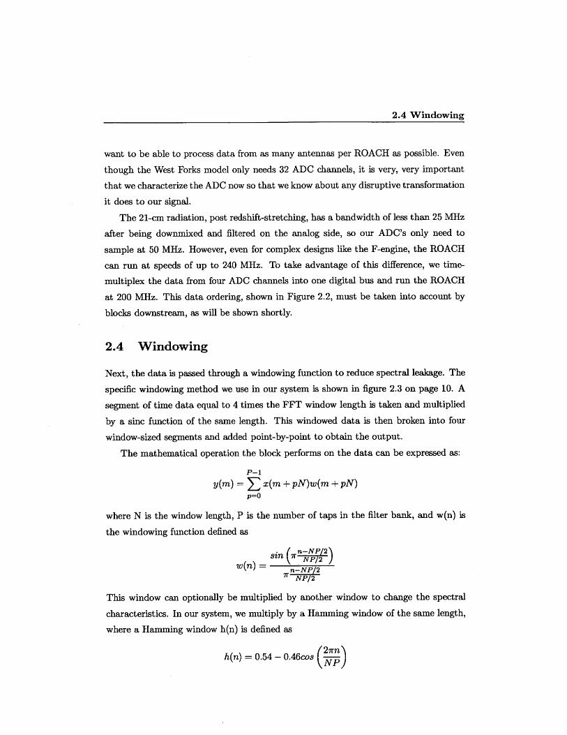
2.4 Windowing
Next, the data is passed through a windowing function to reduce spectral leakage. The
specific windowing method we use in our system is shown in figure 2.3 on page 10. A
segment of time data equal to 4 times the FFT window length is taken and multiplied
by a sinc function of the same length. This windowed data is then broken into four
window-sized segments and added point-by-point to obtain the output.
The mathematical operation the block performs on the data can be expressed as:
P-1
y(m) = E x(m+ pN)w(m+ pN)p=o
where N is the window length, P is the number of taps in the filter bank, and w(n) is
the windowing function defined as
sin (7n"Nr P)w(n) = n-NP2
NP/2
This window can optionally be multiplied by another window to change the spectral
characteristics. In our system, we multiply by a Hamming window of the same length,
where a Hamming window h(n) is defined as
27rnh(n) = 0.54 - 0.46cos (NP)

2. F-ENGINE
4x(i)
0
-2
0 200 400 a00 a00 1000
x1.00.8 w(i)
0.402
-0 . 2-0.4
0 200 400 600 800 1000
-1
a 200 400 00 a00 1000
3 32 1:x"!a~~~N
0
-1 NwjaN0-2 1010208
Figure 2.3: 4-tap polyphase filtering calculation for FFT length 256 - A segment
of time data equal to 4 times the FFT window length is taken and multiplied by a sinc
function of the same length. This windowed data is then broken into four window-sized
segments and added point-by-point to obtain the output. Image taken from Dale Gary's
lecture notes on radio astronomy (4).
More details on the window calculation can be found in the function pf b-coef f _gen-calc. m
located in the CASPER simulink libraries under mlib-devel/casper-library.
In terms of implementation, this block is an FIR filter with time-varying coefficients,
where the coefficients make up the window. This structure ensures that for every data
point that enters the block, one comes out. The one tweak to the system, as shown
in Figure 2.4, involves spacing the taps out by four times as much to account for the
4-to-1 time-multiplexing from the ADC. Other than that, the block is identical to the
one from the CASPER DSP library.
2.5 FFT
The heart of the F-engine is the FFT block, which changes the time stream data into
Fourier coefficients, i.e., spectra. The FFT performs the calculation
N-1
X(k) = E x(n)e-2xjnk/N
n=0

2.5 FFT
Signal
Figure 2.4: Modified FIR filter - Taps are spaced out by four times as much to account
for the 4-to-1 time-multiplexing of the data
where N is the window length of the FFT, x(n) is the input signal, and k is the frequency
bin number.
The FFT for this design is 210 points long, a number we arrive at by trying to meet
the competing demands of having enough frequency resolution to get good data and
getting the design to fit in the alloted gate space on the ROACH. Since the data is still
4-to-1 time-multiplexed coming out of the polyphase FIR filter, we reorder the data
into 210 length blocks from the same channel before passing it into the FFT. Our input
is also all real, so the positive part of the spectrum for a given FFT will actually be
equal to the complex conjugate of the negative part. The FFT block takes this into
account, so for every 210 real points we pass in, we only get 29 complex points out.
It is worth noting, however, that the complex points take twice as many bits to
represent because of their real and imaginary parts, so there is no reduction in bits/cycle
moving through the system. This 50% reduction in output points per antenna means
that for every two data buses going into the FFT, there is one coming out. Since each
input data bus has time stream data from four antennas, each output bus has spectral
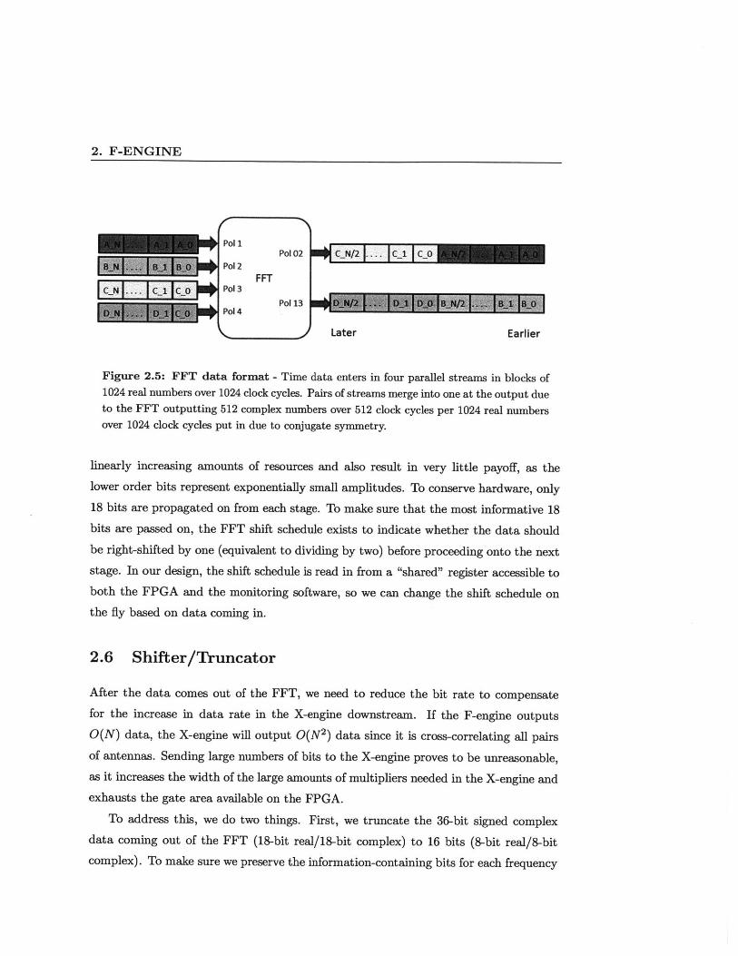
data from eight, interleaved from the two input buses. Figure 2.5 shows the output
ordering, which becomes important downstream when we want to do operations on
specific parts of the spectrum.
Finally, there is the FFT shift schedule to discuss. The FFT consists of a series
of multiplies and adds, each of which increases the number of bits needed to fully
represent the output. Maintaining full precision for the entire FFT would require
2. F-ENGINE
C-N/2..C
Later Earlier
Figure 2.5: FFT data format - Time data enters in four parallel streams in blocks of1024 real numbers over 1024 clock cycles. Pairs of streams merge into one at the output due
to the FFT outputting 512 complex numbers over 512 clock cycles per 1024 real numbersover 1024 clock cycles put in due to conjugate symmetry.
linearly increasing amounts of resources and also result in very little payoff, as the
lower order bits represent exponentially small amplitudes. To conserve hardware, only
18 bits are propagated on from each stage. To make sure that the most informative 18
bits are passed on, the FFT shift schedule exists to indicate whether the data should
be right-shifted by one (equivalent to dividing by two) before proceeding onto the next
stage. In our design, the shift schedule is read in from a "shared" register accessible to
both the FPGA and the monitoring software, so we can change the shift schedule on
the fly based on data coming in.
2.6 Shifter/Truncator
After the data comes out of the FFT, we need to reduce the bit rate to compensate
for the increase in data rate in the X-engine downstream. If the F-engine outputs
O(N) data, the X-engine will output O(N 2 ) data since it is cross-correlating all pairs
of antennas. Sending large numbers of bits to the X-engine proves to be unreasonable,
as it increases the width of the large amounts of multipliers needed in the X-engine and
exhausts the gate area available on the FPGA.
To address this, we do two things. First, we truncate the 36-bit signed complex
data coming out of the FFT (18-bit real/18-bit complex) to 16 bits (8-bit real/8-bit
complex). To make sure we preserve the information-containing bits for each frequency
2.6 Shifter/Truncator
bin, we do a variable, sign-preserving shift before the truncation. This variable shift
allows us to retain information from quiet parts of the spectrum without saturating on
the loud parts.
Bin Number Shift AmountRAM
Data fromshifter
->Truncation
Figure 2.6: Diagram of shifter/truncator - 36-bit data from a different frequency bin
enters from the FFT every clock cycle, and entries in a BRAM determine which 16 bits of
this data are preserved.
All of the processing in the F-engine past the FFT is just data rearranging. There-
fore, we want to put the shift/truncate step as soon after the FFT as possible to reduce
the bit widths of the data buses in as many blocks as possible. To implement the
variable shift, we make use of a counter to track the frequency bin number, i.e. Fourier
coefficient, and the sync pulse, a CASPER convention. A sync pulse fires periodically,
propagating through the entire system and resetting the state of elements it passes
through. The convention is to have the sync pulse travel exactly one clock cycle ahead
of a new data frame, so all blocks are fresh and ready for a new data frame.
For the shifter/truncator, we have the sync pulse reset a counter with 12 bits, where
12 is parameterized as log2 (size of FFT input) +2. The way we arrive at this equation
is that each spectrum is 29 points long, as detailed in section 2.5. However, since there
are also eight different antennas on the bus, it takes 8 x 29 clock cycles per period,

2. F-ENGINE
i.e., 212. Thus, the counter overflows every period. By taking the top three bits of this
counter, we have the channel number, and by taking the bottom nine, we have the bin
number.
We can then feed the bin number into the address port of a RAM, and at the
corresponding location in the RAM, store the amount of left-shift we want for that
particular frequency bin. This shift number feeds into the select line of a multiplexer
whose 0th input is data shifted by 0, 1 st input is data shifted by 1, etc. The output
of the mux is then truncated to the desired bit width. By storing the shift numbers in
a RAM accessible to both the FPGA hardware and the monitoring software, we can
change them in real time based on the data we're receiving.
2.7 Spectrum Divider
Since the X-engine only cares about getting the same spectrum range for all channels,
we can lower the data rate per X-engine even further by parallelizing the correlation
computation. We can divide the spectrum for each antenna into parts, and then only
send a particular part of the spectrum to one of several X-engines. The different cross-
spectra can then be recombined in software afterward.
middle-top fourth middle-bottom fourth bottom fourth k).n
Figure 2.7: Dataflow for spectrum divider module. - Each bar represents a data bus
coming out of the shifter/truncator. Gray parts represent a constant delay to introduce a
phase shift.
We can achieve this division of the spectrum with a few delays and multiplexers.
As shown in Figure 2.7, coming out of the shifter/truncator, we have several buses,
each with some subset of the antennas time-multiplexed on it. What we want in the
middle-bottom fourth I bottom fourth
2.8 Transposer
end is one bus for each section of the spectrum that contains all of the antennas time-
multiplexed, but with only a section of the spectrum for each antenna. By introducing
a different fixed delay for each data bus, we create a phase difference between the
buses, allowing us to use a multiplexer to always have a given part of the spectrum
from the input buses on its output. We then replicate this system with different delays
on different lines, one replica for each part of the spectrum we want to output.
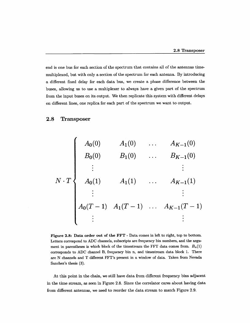
2.8 Transposer
Ao(0) A1 (0) ... AK-1(0)
Bo(O) BI(O) ... BK-1(0)
N -T Ao(1) A1(1) ... AK-1(1)
Ao(T - 1) A 1(T - 1) ... AK-1(T-1)
Figure 2.8: Data order out of the FFT - Data comes in left to right, top to bottom.
Letters correspond to ADC channels, subscripts are frequency bin numbers, and the argu-
ment in parentheses is which block of the timestream the FFT data comes from. B,(1)
corresponds to ADC channel B, frequency bin n, and timestream data block 1. There
are N channels and T different FFT's present in a window of data. Taken from Nevada
Sanchez's thesis (3).
At this point in the chain, we still have data from different frequency bins adjacent
in the time stream, as seen in Figure 2.8. Since the correlator cares about having data
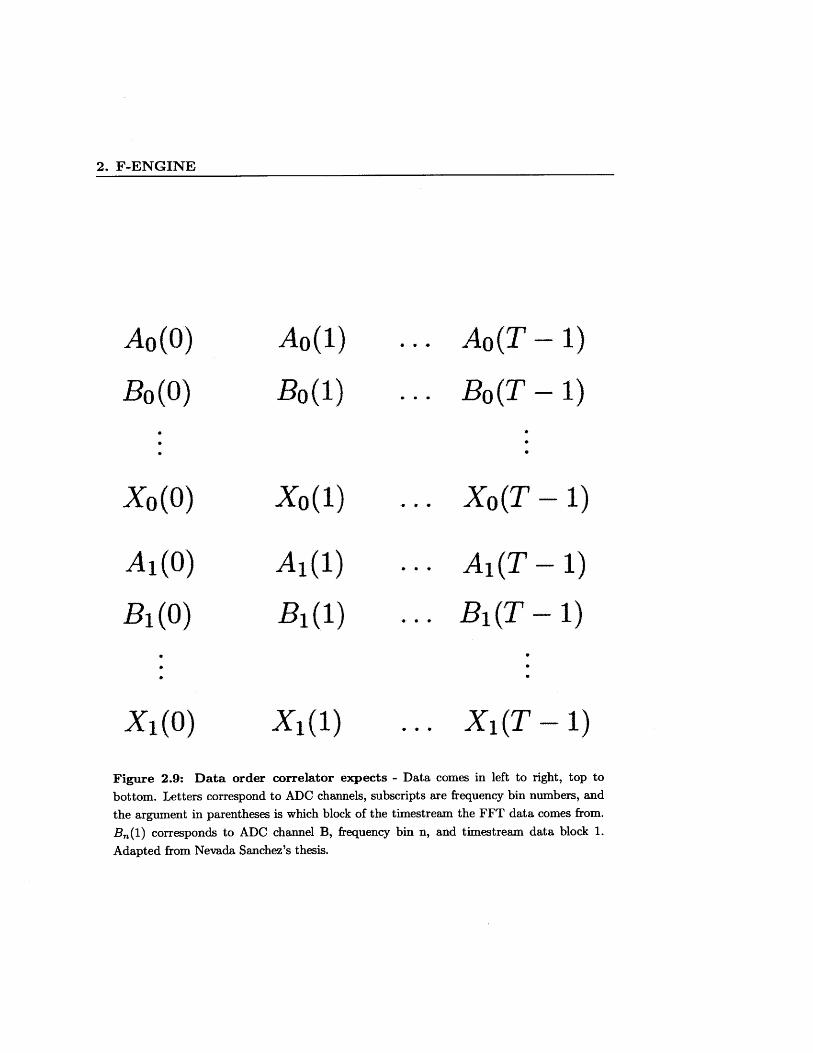
from different antennas, we need to reorder the data stream to match Figure 2.9.
2. F-ENGINE
Ao(T - 1)
Bo(T - 1)
Xo(1)
A1(1)
B1 (1)
X1 (1)
. .. Xo(T - 1)
... A 1(T-1)
B 1(T -1)
0. X1(T-1)
Figure 2.9: Data order correlator expects - Data comes in left to right, top to
bottom. Letters correspond to ADC channels, subscripts are frequency bin numbers, and
the argument in parentheses is which block of the timestream the FFT data comes from.
B,(1) corresponds to ADC channel B, frequency bin n, and timestream data block 1.
Adapted from Nevada Sanchez's thesis.
Ao(O)
Bo(O)
Ao(1)
Bo(1)
Xo(O)
A1 (O)
Bj(O)
X1(O)
2.8 Transposer
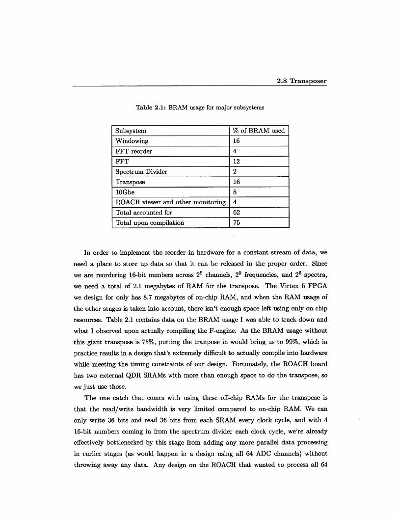
Table 2.1: BRAM usage for major subsystems
Subsystem % of BRAM used
Windowing 16
FFT reorder 4
FFT 12
Spectrum Divider 2
Transpose 16
10Gbe 8
ROACH viewer and other monitoring 4
Total accounted for 62
Total upon compilation 75
In order to implement the reorder in hardware for a constant stream of data, we
need a place to store up data so that it can be released in the proper order. Since
we are reordering 16-bit numbers across 25 channels, 29 frequencies, and 26 spectra,
we need a total of 2.1 megabytes of RAM for the transpose. The Virtex 5 FPGA
we design for only has 8.7 megabytes of on-chip RAM, and when the RAM usage of
the other stages is taken into account, there isn't enough space left using only on-chip
resources. Table 2.1 contains data on the BRAM usage I was able to track down and
what I observed upon actually compiling the F-engine. As the BRAM usage without
this giant transpose is 75%, putting the tranpose in would bring us to 99%, which in
practice results in a design that's extremely difficult to actually compile into hardware
while meeting the timing constraints of our design. Fortunately, the ROACH board
has two external QDR SRAMs with more than enough space to do the transpose, so
we just use those.
The one catch that comes with using these off-chip RAMs for the transpose is
that the read/write bandwidth is very limited compared to on-chip RAM. We can
only write 36 bits and read 36 bits from each SRAM every clock cycle, and with 4
16-bit numbers coming in from the spectrum divider each clock cycle, we're already
effectively bottlenecked by this stage from adding any more parallel data processing
in earlier stages (as would happen in a design using all 64 ADC channels) without
throwing away any data. Any design on the ROACH that wanted to process all 64
2. F-ENGINE
ADC channels would either need to throw away data or avoid using the SRAMs, most
likely by designing and using a cross-correlating block in the X-engine that doesn't need
to do an internal accumulation to compensate for the quadratically increasing number
of outputs With that requirement relaxed, we wouldn't require multiple samples from
the same channel and frequency to be fed in sequentially in time.
2.9 10-Gigabit Ethernet
The correlator spans across multiple ROACHes, with F-engines and X-engines inhabit-
ing separate boards. To move data between them, we use 10-Gigabit ethernet (10Gbe).
The protocol for sending data out with the 10Gbe block can be found on the
CASPER wiki, but it is repeated here for completeness. The transmitting block takes
in a 64-bit data bus, and a 1 bit valid line marks which clock cycles actually contain
data to be sent. This data is placed in a FIFO buffer. Since data is sent in packets,
we also need to tell the block when to send out the contents of its buffer. This is done
with the "end of frame" line, which is pulsed high on the same clock cycle of the valid
high for the last 64-bit word we want in the packet.
Each packet has a header attached to it containing metadata such as the packet's
source, destination, size, and an error detection checksum. Since each packet, regardless
of its message length, has a constant size header attached to it, we want to make sure
our ratio of header data to signal data is not so large that we don't have the bandwidth
to send all of the signal data we want to. A packet size of 512 64-bit words has proven
sufficient to meet our needs.
One issue that plagued us during development was the occasional insertion of an
extra 64-bit word in the first packet sent out after startup. The data in this extra word
varied: sometimes it was all zeros; sometimes it was dependent on the data being sent
in; sometimes it was random. The other point to stress is that this extra word only
showed up sometimes: restarting the system would not reliably produce or erase the
extra word. Because of our system's streaming data architecture, an insertion of an
extra word throws off the alignment of all the processing downstream, creating false
patterns in the output data.
This set of inconsistent behaviors across resets, paired with the changing of clock
domains from the FPGA's 200 MHz to the 10Gbe 156.25 MHz, all points to a race
2.10 Monitoring BRAM
condition. A race condition is when the behavior of a system depends on how quickly
two or more electrical signals propagate relative to each other. Also, since this extra
word only shows up once and in the very first packet, it suggests that something odd
occasionally happens when the 10Gbe hardware is starting up. Since so many poorly-
characterized factors are at play here, the outcome in any given instance is effectively
random to us.
Unfortunately, we don't have a good enough understanding of the inner workings of
the 10Gbe block to get to the core of what's causing this problem. For the time being,
we took advantage of the ROACH's powerful hardware/software interfacing to create a
workaround. Although we can't predict whether the extra word will be inserted or not
in advance, we can detect in software whether it was inserted after the fact. If there
was an insertion, we keep resetting and checking until there is no insertion.
2.10 Monitoring BRAM
As sections 2.5 and 2.6 mentioned, there are some shift parameters we can change in
real time based on the data being processed. In order to intelligently determine these
shifts, we need to be able to see the data at certain points in the processing chain. It
is also generally useful to be able to see data at all points in the system for debugging
purposes. We can do this with a "snap" block from the CASPER library, which allows
us to take timed snapshots of data into a BRAM whose contents can also be read by a
computer hooked up to the ROACH.
We have but a single snap for the whole system, but we multiplex every data line
we'd ever want to look at into the data in port of the snap, aligning data as necessary
to fit in the fixed 32-bit wide RAM. Since most of our data is signed, we pad zeros
onto the least significant bits to line up the sign bit of the data with the sign bit of the
location where its stored. We control the select line of the multiplexer with a register
that we can write to from the computer, so we can grab data from wherever we please
while the design is running. To ensure that we see the same part of the data frame
across different BRAM reads, we trigger the snap to read off of the sync pulse, which
will always arrive one cycle before a fresh data frame.
The software that reads from this monitoring BRAM and displays the data is cov-
ered in detail later in the ROACH viewer section.

2. F-ENGINE

3
X-Engine
3.1 Purpose
The X-engine performs a cross-correlation between all pairs of channels for some subset
of the frequencies output by the FFT done in the F-engine. Between our four X-engines,
we cover all 512 of the frequency bins and thus process our entire 25 MHz bandwidth
taken in from the ADC. These cross-correlations are then accumulated to reduce the
variance of noise and lower the data rate so that we can ship data out to software.
3.2 Overview
10 Buffer Cross- Vector To rxgbe correlator accumulator software
Figure 3.1: Block diagram of X-engine - Data comes in from the F-engine via 10-Gigabit ethernet, is buffered and then all channels are cross-correlated within each fre-
quency bin. These correlations are accumulated for a user-defined period of time and then
exported to the receiving software.
Data comes in from the F-engine via a 10Gbe receiving block. The data rate is

3. X-ENGINE
smoothed out into a stream with a buffer and then fed into the cross-correlator block.
The completed correlations are then fed into an accumulator which in turn places its
output in snap blocks to be read out by software.
3.3 10Gbe Receiving System
The data from the F-engine comes out of a 10Gbe receiving block in a similar way to
how it was put in: a 64-bit data bus presents data every clock cycle, with a valid line
representing whether this data is new data from the 10Gbe link. The last word of a
packet is also accompanied by a pulse from the end-of-frame line. Since the FPGA is
clocked at a faster, non-integer multiple of the 10Gbe clock, there is no quick and easy
way to output a continuous stream of data for the downstream elements to process.
Additionally, delays incurred from the physical 10Gbe link add unpredictable jitter to
the rate at which we receive data. Thus, we need a buffer to smooth the data flow into
periodic, back-to-back windows of data for the cross-correlator to process.
Since we're working with hardware, we don't have the option of explicitly telling
the correlator block to wait until we have enough data for a window. The streaming
architecture of our system means that it will be processing something no matter what,
so we need to make sure that we know which computations to save and which to ignore.
It should be emphasized that sending junk data into cross-correlator block won't cause
any problems as long as there is no junk data in windows with valid data and vice
versa. As long as this condition holds, we can mark junk data as such when it goes
into the correlator and ignore the corresponding output.
To create these windows of valid and junk data, we put valid data as it comes in
from the 10Gbe into a FIFO. Using the sync pulse, we synchronize a counter to the
cross-correlator such that it overflows every time the correlator wants a new window of
data. Whenever this counter overflows, we check if the FIFO has enough data to send
out a window of valid data. If it does, we send one out. If it doesn't, we send out a
window of junk data consisting of all 1's and mark it as such by holding the valid line
low.
With this buffering system in place, we are resilient to underflows of data from the
F-engine, as our buffer will just continue to spit out windows of junk data until it has
stored up enough valid data. However, we are not resilient to overflows: the FIFO has
3.3 1OGbe Receiving System
Data from Buffered data10gbe
Bufe
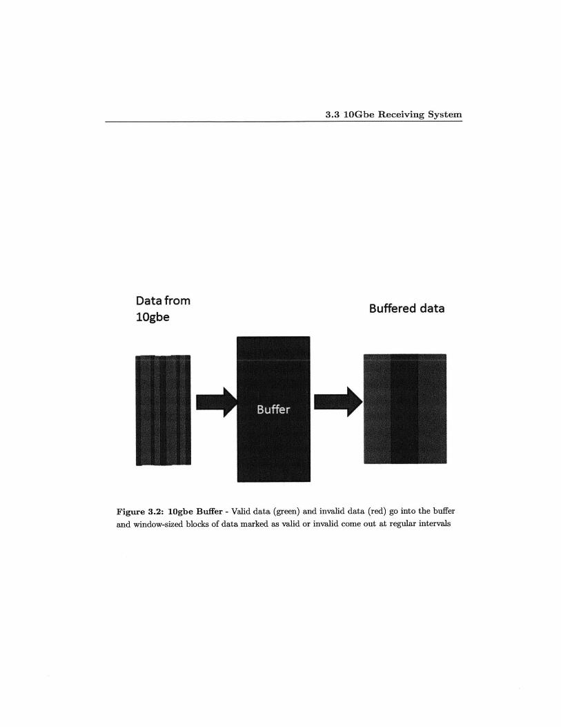
Figure 3.2: 10gbe Buffer - Valid data (green) and invalid data (red) go into the buffer
and window-sized blocks of data marked as valid or invalid come out at regular intervals
3. X-ENGINE
finite size, and if it ever overflows, we will lose data and throw all of our synchronization
off. Another point of note is that the FPGA clocks of the F-engines and the X-engines
are not coupled in any way, so even if they are both nominally set to 200 MHz, there
is almost certainly a small (0.0001%) difference between them one way or the other. If
the correlator is run for long periods of time, this difference can result in one of the
FPGAs getting ahead of the other, and if it's the F-engine, we can get overflows. To
keep our design asynchronous between F and X-engines, we simply clock our X-engines
at 201 MHz to ensure that they will underflow and never overflow.
3.4 Cross-correlator
The cross-correlator takes data from each channel for a given frequency bin and finds
the cross-correlation AB* for each pair of channels. The particular implementation we
use in our system was developed by Nevada Sanchez, a former Master's student on the
project. For more details on the design and inner workings of the block, consult his
Master's thesis (3). The aspects of the block relevant to this thesis are the constraints
that it places on the rest of the system. As discussed in section 2.8, most of the data
rearranging done between the FFT and the cross-correlator is due to the difference
between how the FFT outputs data and how the correlator receives it. For every 2048
points that the correlator takes in (32 channels of a particular frequency bin collected
from 64 different FFT's), the correlator outputs 528 baselines for that frequency to the
vector accumulator. The factor of 64 is important, as it is how large of an internal
accumulation the cross-correlator performs. This will then be compounded by a mul-
tiplicative factor with an even bigger accumulation in the next processing stage, the
vector accumulator.
3.5 Vector Accumulator
The vector accumulator (VACC) is used to both average the data over time to reduce
noise and to reduce the data rate to a level that a computer can read. We specify a
vector length of N, and then samples of the same time index mod N are accumulated
together. The user specifies a number of vectors to accumulate, ranging from the
minimum default value of 1024 to a maximum value of 8192. The minimum value

3.5 Vector Accumulator
comes from a constraint from the transmitting software that follows after, discussed
in section 4.3, while the maximum value is largest we can have without potentially
overflowing in our accumulation math due to running out of bits for a given address
in the VACC. This number, when multiplied by the internal accumulation from the
cross-correlator, gives us the total number of samples we have accumulated for each
index of the output vector.
The VACC then outputs the accumulated data into a BRAM that the receiving
software can read from. Since we have 128 frequencies per X-engine, we need a vector
length of 128 * 528 = 67584 to keep track of each baseline at each frequency. Due the
large size of these vectors, we use the QDR rams to store them, one for the real part
of the baselines and one for the imaginary. For the default VACC accumulation length
of 1024, we get a finished accumulation every
vectors freqs window cycles sec seconds1024 *128 *1 *2048 *5x10 = 1.36
accum vector frequency window cycle accumulation
where the 2048 length window is the cross-correlator window and implies that a 64-fold
accumulation has taken place inside of the cross-correlator.
654321 4 5 6
MO+M 2 +
Figure 3.3: Vector accumulator for vector length 3 - Data comes in from the right
serially, accumulating in different elements of the vector until it reaches the end, at which
point it loops back to the first element.

3. X-ENGINE
4
Transmitting and Receiving
Software
4.1 Purpose
The receiving software exists to transmit the data from the X-engine ROACHes to a
computer of our choice via normal gigabit ethernet. One challenge comes from the fact
that the X-engine outputs its processed data in small, semi-regular bursts to save on
hardware resources, so the software must infer when one accumulation's data ends and
the next begins and also stitch a given accumulation's data back together.
4.2 Overview
Processed data is dumped from the X-engine's vector accumulator into a small shared
BRAM to be read by the transmitting software. The transmitting software gathers
up an entire accumulation's worth of data in RAM, then breaks it into packet-sized
chunks and sends them out over ethernet via the UDP protocol. The receiving software
collects these packets, assembles them back into accumulations, and writes them to an
.odf file for viewing.
4.3 Transmitting Software
The transmitting software's job is to read the data from the FPGA and send it out via
ethernet from the ROACH's on board PowerPC to another computer. The gateway

4. TRANSMITTING AND RECEIVING SOFTWARE
Figure 4.1: Block diagram of software chain - The X-engine outputs accumulated
baselines, which the transmitting software running on the ROACH reads. It sends the data
via UDP to a PC that stores up the data and writes out files for viewing later.
between the FPGA and the PowerPC is the shared BRAM that either platform can
read or write to. Since the X-engine's vector accumulator is not putting out data at
a high rate, we can use a very small shared BRAM to save on resources. To read out
an accumulation, whenever the BRAM is empty, the vector accumulator dumps data
into the BRAM until it is filled. The transmitting software periodically checks how full
the BRAM is and empties it, storing the data in CPU RAM. This filling and emptying
repeats until the vector accumulator has written its entire accumulation of data out.
If the BRAM is emptied and remains empty for a long enough time, we take that as
a signal that the vector accumulator is done with that accumulation. We then take the
data, divide it up into packets, and send them out over ethernet via the UDP protocol.
Each packet is tagged with the time stamp of the accumulation it came from and an
offset indicating which part of the accumulation it contains.
When adapting this software to run on four X-engines simultaneously, I had to
work around the issue of packet collision. Before, we only had one UDP sender and one
UDP receiver, so allocating communication time on the network was trivial. However,
four X-engines means four UDP senders, all wanting to send at the same time due to

4.4 Receiving Software
the F-engine sending data at the same rate and time to each of them. If two senders
attempt to send a packet at the same time, a packet collision occurs, and one or both
of the packets can be lost.
The first solution I tried was to move from the UDP protocol, which blindly sends
packets without verifying that they arrive at their destination, to the TCP protocol,
which attempts to verify that packets are received and resends if they are not. TCP
has more overhead, both in implementation complexity and network usage, but it does
avoid packet collision when it works properly. Unfortunately, due to time constraints
and a lack of experience, I wasn't able to implement TCP.
Fortunately, TCP wasn't actually needed to solve this particular problem. Since
our senders transmit periodically, we can just increase the period by a factor of four
and have them take turns sending. The tradeoff is that the transmitting software has
to buffer more data in RAM, but PowerPC RAM was very underutilized before, so this
is not a problem. The timestamps of the accumulations are more or less synchronized
between the X-engines, so we use those to determine whose turn it is to send. X-engine
0 sends the past four accumulations every timestamp 0 mod 4, X-engine 1 sends every
timestamp 1 mod 4, and so on. This setup drastically reduces the amount of collisions
that happen.
While the time-multiplexing helps with packet collision a good deal, it doesn't
completely eliminate it, and we don't want to lose any data to packet collisions. With
just time-multiplexing, we found that a few packets, around one in a thousand, would
still be lost. Notably, there was no particular pattern to which packets were lost. The
solution we settled on was to send data twice in a row. Since each packet has all
of the information needed to determine exactly which accumulation it belongs to and
what part of the accumulation it represents, the receiving software can safely identify
and ignore packets with redundant information. With this solution, one in a million
accumulations will still be missing a packet, but the receiving software handles this by
simply writing all zeroes if it detects this.
4.4 Receiving Software
The receiving software's job is to take in the packets sent from the PowerPC, recon-
struct the accumulation they represent, and then package this data into Omniscope
4. TRANSMITTING AND RECEIVING SOFTWARE
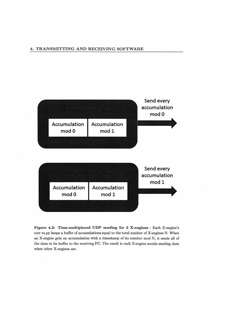
Figure 4.2: Time-multiplexed UDP sending for 2 X-engines - Each X-engine's
corr tx.py keeps a buffer of accumulations equal to the total number of X-engines N. When
an X-engine gets an accumulation with a timestamp of its number mod N, it sends all of
the data in its buffer to the receiving PC. The result is each X-engine avoids sending data
when other X-engines are.
4.4 Receiving Software
data format (.odf) files to be read later. In the one sender, one receiver case, this is a
fairly simple operation, as the data arrives nicely in order and is easily reconstructed.
Each packet has the number of the accumluation it's from and an offset that indi-
cates what part of the accumulation it represents. The receiving software allocates an
accumulation-sized space and places the packets in their places as they arrive based on
the offsets. When a packet with a new accumulation timestamp arrives, the software
checks that it has all the numbers from the last accumulation and if it does, it adds
that accumulation as a new timeslice to the output .odf file. If it's missing numbers,
it writes all zeros for that timeslice and proceeds to the next one. However, the trans-
mitting software is robust enough that this should only happen about one in a million
times, and has never actually been observed in practice.
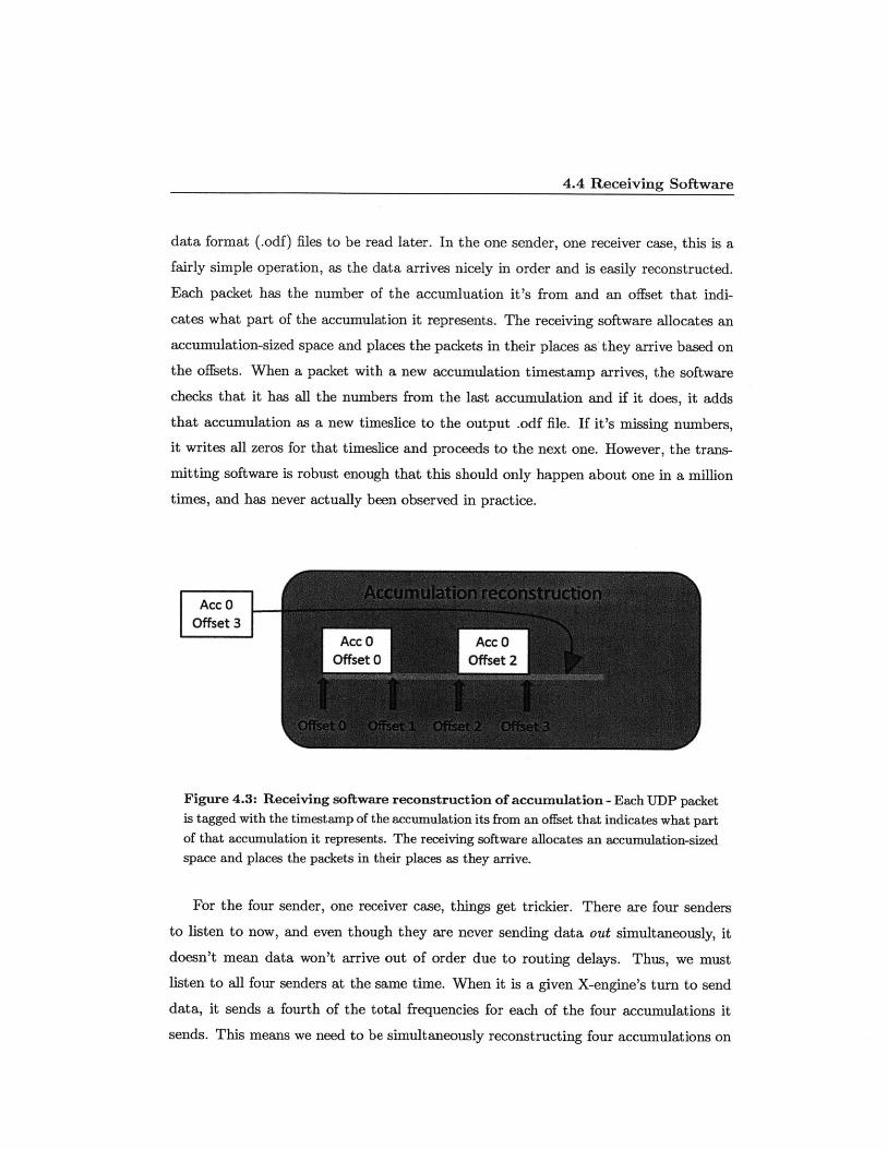
Acc 0Offset 3
Acc 0 Acc 0offset 0 Offset 2
Figure 4.3: Receiving software reconstruction of accumulation - Each UDP packetis tagged with the timestamp of the accumulation its from an offset that indicates what partof that accumulation it represents. The receiving software allocates an accumulation-sizedspace and places the packets in their places as they arrive.
For the four sender, one receiver case, things get trickier. There are four senders
to listen to now, and even though they are never sending data out simultaneously, it
doesn't mean data won't arrive out of order due to routing delays. Thus, we must
listen to all four senders at the same time. When it is a given X-engine's turn to send
data, it sends a fourth of the total frequencies for each of the four accumulations it
sends. This means we need to be simultaneously reconstructing four accumulations on
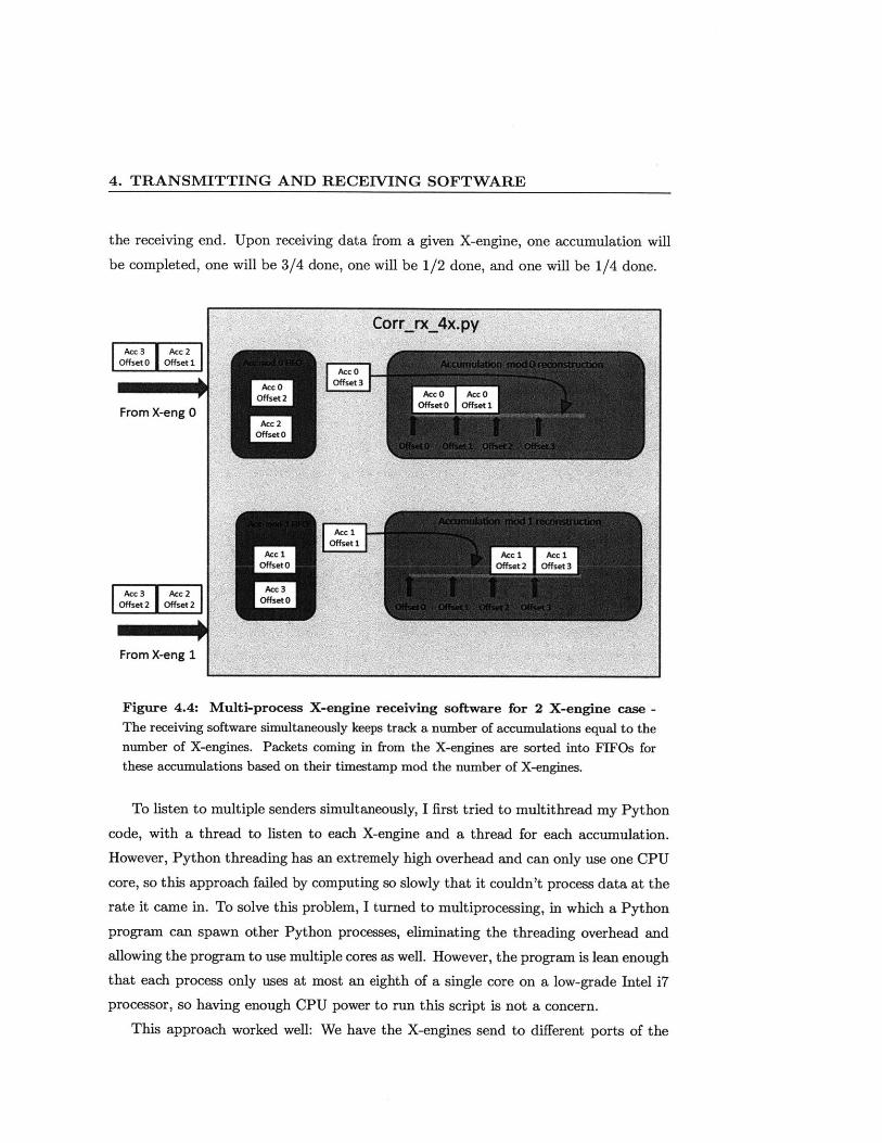
4. TRANSMITTING AND RECEIVING SOFTWARE
the receiving end. Upon receiving data from a given X-engine, one accumulation will
be completed, one will be 3/4 done, one will be 1/2 done, and one will be 1/4 done.
Figure 4.4: Multi-process X-engine receiving software for 2 X-engine case -The receiving software simultaneously keeps track a number of accumulations equal to thenumber of X-engines. Packets coming in from the X-engines are sorted into FIFOs forthese accumulations based on their timestamp mod the number of X-engines.
To listen to multiple senders simultaneously, I first tried to multithread my Python
code, with a thread to listen to each X-engine and a thread for each accumulation.
However, Python threading has an extremely high overhead and can only use one CPU
core, so this approach failed by computing so slowly that it couldn't process data at the
rate it came in. To solve this problem, I turned to multiprocessing, in which a Python
program can spawn other Python processes, eliminating the threading overhead and
allowing the program to use multiple cores as well. However, the program is lean enough
that each process only uses at most an eighth of a single core on a low-grade Intel i7
processor, so having enough CPU power to run this script is not a concern.
This approach worked well: We have the X-engines send to different ports of the
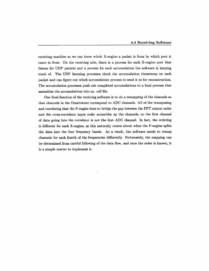
4.4 Receiving Software
receiving machine so we can know which X-engine a packet is from by which port it
came in from. On the receiving side, there is a process for each X-engine port that
listens for UDP packets and a process for each accumulation the software is keeping
track of. The UDP listening processes check the accumulation timestamp on each
packet and can figure out which accumulation process to send it to for reconstruction.
The accumulation processes push out completed accumulations to a final process that
assembles the accumulations into an .odf file.
One final function of the receiving software is to do a remapping of the channels so
that channels in the Omniviewer correspond to ADC channels. All of the transposing
and reordering that the F-engine does to bridge the gap between the FFT output order
and the cross-correlator input order scrambles up the channels, so the first channel
of data going into the correlator is not the first ADC channel. In fact, the ordering
is different for each X-engine, as this naturally comes about when the F-engine splits
the data into the four frequency bands. As a result, the software needs to remap
channels for each fourth of the frequencies differently. Fortunately, the mapping can
be determined from careful following of the data flow, and once the order is known, it
is a simple matter to implement it.
4. TRANSMITTING AND RECEIVING SOFTWARE
5
ROACH Viewer
5.1 Purpose
Any system needs to be debugged once it's implemented, if nothing else to verify that
it is operating correctly. To do this with the F-engine, we need to be able to look at
the data after it is processed by each stage. The shared BRAMs that both the FPGA
and the PowerPC can read from and write to play a key role in this process, as they
allow us to do exactly what we want to. By feeding data into these shared BRAMs
from the various stages of the F-engine, we can feed in known inputs and verify that
the F-engine produces the expected output at each juncture.
Furthermore, when using the correlator on real input when the exact nature of the
data is unknown, we can look at the data as it is being processed to ensure that its
dynamic range is not so large as to be unrepresentable with the number of bits we have.
If we observe this happening, we can adjust the processing stages to scale down the
data. Conversely, if we observe that the data has a very small dynamic range, we can
scale the data up to fully utilize the resolution that the number of bits we have affords
us. The software we use to record the data from the ROACH, display it, and adjust
these scaling gains is known as the ROACH Viewer.
5.2 Overview
The proper operation of the ROACH Viewer involves coordination in design between
the hardware and the software. The details of the hardware side implementation are
discussed in section 2.10.
5. ROACH VIEWER
On the software side, the ROACH Viewer runs on a software framework developed
by Nevada Sanchez, a previous Master's student in the group (3). This ViewerCore
framework provides for a shell that continuously calls a plot-update function to acquire
and plot new data from the ROACH. It is up to the system designer to then create
a plot-update function for his or her specific hardware, which involves doing any
necessary setup, acquiring the data, parsing it, and plotting it.
me
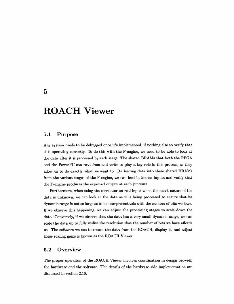
Figure 5.1: Screenshot of the ROACH Viewer - The tabs at the top allow the user
to switch between the different processing stages of the F-engine. The various elements
at the bottom allow the user to adjust the viewing options on the plot and modify the
processing the F-engine does to avoid saturating or to fully use the resolution the bits at
that stage offers.
My implementation of the ROACH Viewer, pictured in Figure 5.1 on page 36, allows
the user to see the F-engine's data on all 32 channels for the ADO, windowing, FFT,
and shifter/truncater stages. Since properly aligning data from these stages depends
on capturing the data right after the sync pulse that precedes the first piece of valid
data in a window, it becomes difficult to view our data after the transposing operations
that increase the window size by a factor of 64. Thus, the ROACH Viewer doesn't
show data past the shifter/truncater stage or from the X-engine.
6
Swapper
6.1 Purpose
Our ADC is not ideal. One problem it has is cross-talk between channels due to the
physical proximity of the cables carrying signal into the ADC: the changing electric
fields in one cable create magnetic fields which in turn induce electric fields in other
cables that are dependent on the signal in the original cable. To deal with this problem,
we have set up a system to invert a rotating subset of the analog signals right after
they leave the antenna such that each signal is inverted 50% of the time relative to all
of the other signals. We then de-invert those signals inside of the FPGA right after
they're captured by the ADC. Thus, any cross-talk gets canceled out during our time
averaging operations. For a detailed and rigorous treatment of the subject, including
our use of Walsh functions, consult Nevada Sanchez's Master's of Engineering thesis
(3).
6.2 Overview
Our swapper system interacts with the signal at two points: inverting the analog sig-
nal right after the antenna and de-inverting the digital signal right after it enters the
FPGA. There needs to be some sort of master controller that is keeping track of what
channels are getting swapped when, that sends out signals to the hardware doing the
analog and digital swapping. Since our signals are going into a giant piece of pro-
grammable hardware, it makes sense to put this master controller on the FPGA. We
can then program our swapping pattern to the shared BRAM on the FPGA and have
6. SWAPPER
the master controller send that pattern out to the analog and digital swappers. Sending
to the digital swapper is easy, as the signals stay inside of the FPGA. Sending to the
analog swapper is harder, as we need to create control signals for the physical swapping
hardware and send them out via the general purpose in/out (GPIO) pins on the FPGA.
6.3 Digital swapping
The digital side of the swapping system starts with a shared BRAM that we program
our swapping pattern to. At any given point in time, we need one bit per channel to
indicate whether to swap that channel or not. Thus, we can represent the instantaneous
swap state of our 64 channels with a 64-bit word, with the 0th bit corresponding to the
0th channel and so on. The swap pattern is also time-dependent, so we put a 64-bit
word in a different address of the BRAM for each time step we want to be able to
represent. By feeding the desired time step into the address port of the BRAM, we
can retrieve the desired swap state at that instant. Then we can use the bit for each
channel to control whether to swap the digital signal or not.
6.4 Analog swapping
The analog side of the swapping starts from the same place as the digital: the BRAM
where our swapping pattern is stored. The same storage convention holds true here as
well, but the process of getting this data to the hardware doing the swapping is more
involved. The physical hardware that controls the analog swapping is outside of the
FPGA, and in order to communicate with it, we need to send it signals via the GPIO
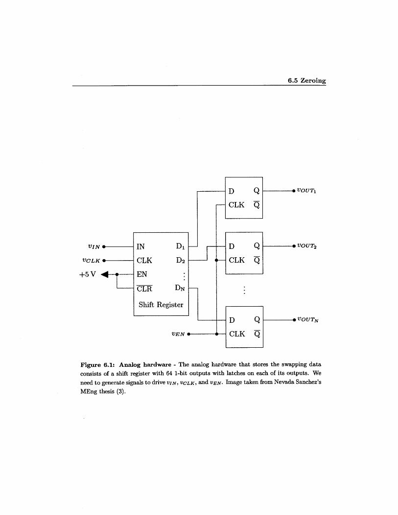
pins. The analog hardware that stores the swapping data consists of a shift register
with 64 1-bit outputs with latches on each of its outputs. From the FPGA, we need to
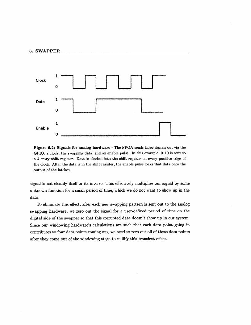
generate a clock for this hardware, a data signal, and an enable pulse for the latches.
This is best expressed in a diagram, so figure 6.2 on page 40 contains a diagram of the
desired signals and timing and an explanation of where they come from.
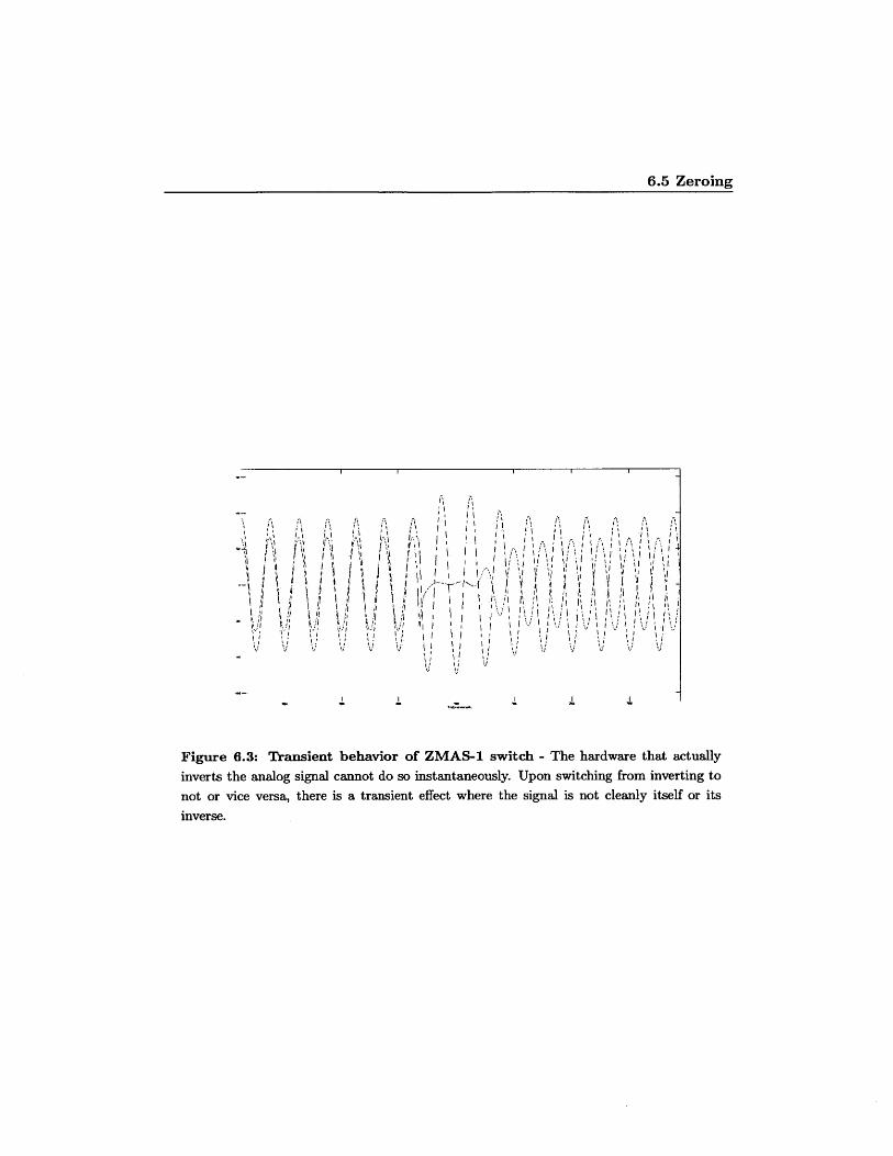
6.5 Zeroing
The hardware that actually inverts the analog signal cannot do so instantaneously.
Upon switching from inverting to not or vice versa, there is a transient effect where the
6.5 Zeroing
D Q vouT,
-CLK Q
F IN . IN D - - D tha --- e out2
VCLK 0- -- CLK D2 CLK Q
+5 V EN4 :
-C~R DN
Shift Register
D Q 9 VOUTN
UEN 00CLK q
Figure 6.1: Analog hardware - The analog hardware that stores the swapping data
consists of a shift register with 64 1-bit outputs with latches on each of its outputs. We
need to generate signals to drive VIN, VCLK, and yEN. Image taken from Nevada Sanchez's
MEng thesis (3).
6. SWAPPER
1Clock
Data
0
Enable
0
Figure 6.2: Signals for analog hardware - The FPGA sends three signals out via the
GPIO: a clock, the swapping data, and an enable pulse. In this example, 0110 is sent toa 4-entry shift register. Data is clocked into the shift register on every positive edge ofthe clock. After the data is in the shift register, the enable pulse locks that data onto the
output of the latches.
signal is not cleanly itself or its inverse. This effectively multiplies our signal by some
unknown function for a small period of time, which we do not want to show up in the
data.
To eliminate this effect, after each new swapping pattern is sent out to the analog
swapping hardware, we zero out the signal for a user-defined period of time on the
digital side of the swapper so that this corrupted data doesn't show up in our system.
Since our windowing hardware's calculations are such that each data point going in
contributes to four data points coming out, we need to zero out all of those data points
after they come out of the windowing stage to nullify this transient effect.
-7
V~ V' V~ I
Figure 6.3: Transient behavior of ZMAS-1 switch - The hardware that actually
inverts the analog signal cannot do so instantaneously. Upon switching from inverting to
not or vice versa, there is a transient effect where the signal is not cleanly itself or its
inverse.
6.5 Zeroing
1 V "
Ii
ii 'I
A Iii I
/ 1
I,'
I II

6. SWAPPER

7
64-Channel F-engine
7.1 Purpose
The Omniscope is designed to have as low of a cost per antenna as possible, and to that
end, we have an ADC board that allows each Roach to take in 64 channels of analog
data, minimizing the digital signal processing cost of each antenna. The 32-channel
design was a jump forward in that it introduced cross-Roach communication and 8 bits
of precision. The 64-channel design aims to retain those gains while fully utilizing the
Roach for maximum efficiency.
7.2 Overview
I was fortunate to have enough time and luck to implement a digital backend capable
of handling twice as many ADC channels. The key problem that the 64-channel design
introduces occurs in the F-engine at the transposing step. As mentioned in section
2.8, the 32-channel F-engine is already using the full bandwidth of the QDR SRAMs
that are used to do part of the transpose. If we double the number of channels, we
need to throw out half of our data in some sense. We first tried to throw out half of
the frequency data from the FFT, but the additional hardware needed to do twice as
many FFTs proved to be too much to fit on the FPGA. In the end, we settled for only
taking FFTs of any given channel half of the time, throwing out half of our timestream
data. By reducing the data rate very early in the processing chain, we saved enough
resources to fit a 64-channel design on the Roach.
7. 64-CHANNEL F-ENGINE
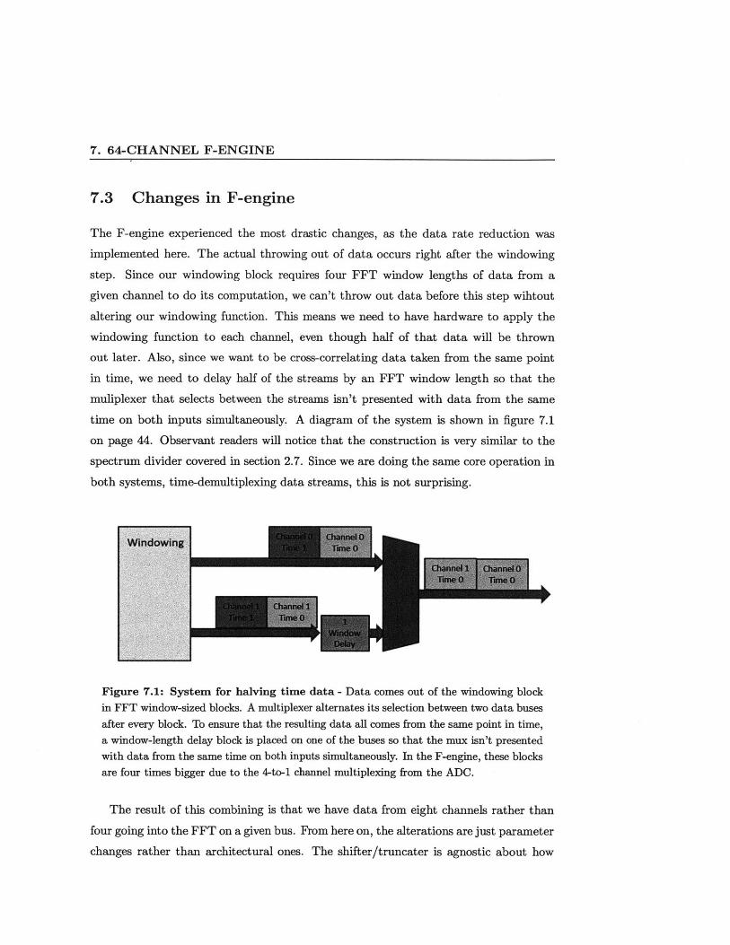
7.3 Changes in F-engine
The F-engine experienced the most drastic changes, as the data rate reduction was
implemented here. The actual throwing out of data occurs right after the windowing
step. Since our windowing block requires four FFT window lengths of data from a
given channel to do its computation, we can't throw out data before this step wihtout
altering our windowing function. This means we need to have hardware to apply the
windowing function to each channel, even though half of that data will be thrown
out later. Also, since we want to be cross-correlating data taken from the same point
in time, we need to delay half of the streams by an FFT window length so that the
muliplexer that selects between the streams isn't presented with data from the same
time on both inputs simultaneously. A diagram of the system is shown in figure 7.1
on page 44. Observant readers will notice that the construction is very similar to the
spectrum divider covered in section 2.7. Since we are doing the same core operation in
both systems, time-demultiplexing data streams, this is not surprising.
Windowing
Figure 7.1: System for halving time data - Data comes out of the windowing blockin FFT window-sized blocks. A multiplexer alternates its selection between two data busesafter every block. To ensure that the resulting data all comes from the same point in time,a window-length delay block is placed on one of the buses so that the mux isn't presentedwith data from the same time on both inputs simultaneously. In the F-engine, these blocksare four times bigger due to the 4-to-1 channel multiplexing from the ADC.
The result of this combining is that we have data from eight channels rather than
four going into the FFT on a given bus. From here on, the alterations are just parameter
changes rather than architectural ones. The shifter/truncater is agnostic about how
7.4 Changes in X-engine
many different channels are going through it, as it performs all of its operations within
an FFT frame. The spectrum divider also doesn't change for the same reason. The
transposing system needs to change the size of its transpose, but the data rate is the
same as in the 32-channel F-engine by design, so the transpose size is all that changes.
Finally, the 10gbe transmission system doesn't care about what it's sending so that
remains the same as well.
7.4 Changes in X-engine
The X-engine receives entirely parametric updates. The size of a window of data
for the cross-correlator is the number of channels times the internal cross-correlator
accumulation length, so the 10gbe buffer and cross-correlator window sizes need to be
changed from 2048 to 4096. Clever parameterization in the design of these blocks makes
this an easy task. The number of baselines the vector accumulator needs to keep track
of also depends on the number of channels, so it increases from 128* 32* 33/2 = 67584
to 128 * 64 * 65 * 2 = 266240. Since we're using the large QDR SRAM to store the
vector accumulator's data, we can handle this increase in storage requirement easily.
7.5 Changes in receiving software
The transmitting and receiving scripts both care about the number of baselines, which
depends on the number of channels, so they needed to be updated accordingly. Again,
parameterization of the code makes it mostly a matter of changing one variable. The
one catch is that in the new system, there is a lot more data to read from the vector
accumulator. In the 32-channel design, the vector accumulator completes an accumu-
lation every 1024 * 128 * 2048 clock cycles, where 1024 is an accumulation length we
can set freely, 128 is the number of frequencies we range over, and 2048 is the length
of a cross-correlator window in clock cycles. In this amount of time, the receiving
software is barely able to retrieve the 128 * 32 * 33/2 = 67584 data points it needs to
before the next accumulation comes in. When we double the number of channels, we
are quadrupling the number of data points we need to retrieve while only doubling the
period in which new data comes in. As a result, the minimum vector accumulation
length we can have to get the data out in time doubles from 1024 to 2048, resulting
7. 64-CHANNEL F-ENGINE
in accumulations coming out every 5.45 seconds. The width of addresses in the VACC
has not changed, so the maximum accumulation length is still 8192, corresponding to
accumulations every 22 seconds.

8
Quad F-engine Roadmap
8.1 Purpose
The more antennas our system can support, the larger effective collecting area our
telescope has and the more scientifically useful it is. Our lab currently has eight Roach
boards, so to fully utilize our available hardware, we want a design with 4 F-engines
and 4 X-engines. If each F-engine is a 64-channel model, this will allow our telescope
to process data from 64 dual polarization antennas.
8.2 Overview
When working with multiple F-engines, the first concern is clocking the ADCs syn-
chronously. As mentioned in section 7.3, it is important that we cross-correlate data
taken from the same point in time. To ensure that the four ADCs are consistently
sampling with the same period and at roughly the same point in time, we need to
generate a single clock and split and distribute it to the ADCs. In a first pass overview,
not much changes about the F-engine other than a need for some sort of infrequent,
periodic pulse sent to all four F-engines so that when they are reset, they all start at
the same time. Since each X-engine is taking data from four times as many F-engines
in this design, changes need to be made to account for the increase in data load.

8. QUAD F-ENGINE ROADMAP
8.3 Clocking
Our clocking solution was devloped by Kevin Zheng with help from Devon Rosner,
undergraduates in the group. An overview diagram is shown in figure 8.1. It starts
with a 10 Megahertz clock generated by a Trimble Thunderbolt E clock generator,
chosen for the stability of its clock. This feeds into a Valon Technology 5007 frequency
synthesizer, which can be programmed via USB to output frequencies from 140 MHz to
4 GHz. The minimum frequency of 140 MHz is still larger than our desired frequency
of 50 MHz, so we have the 5007 output 200 MHz and and feed that clock into a Valon
Technology 3008 Frequency Divider set to divide it down to 50 MHz.
10 MH z20MHz
uenderbolt Valon 5007 Valon 3008
o200 MHz 50 MHz 50 MHzF-engine ROACH 0 F-engine ADC 0
F-engine ROACH 1 F-engine ADC 1 RDCLK854
F-engine ROACH 2 F-engine ADC 2
F-engine ROACH 3 F-engine ADC 3**
Figure 8.1: Clock distribution system - The Trimble Thunderbolt generates a 10 MHz
clock. This is turned into a 200 MHz clock by the Valon 5007, which in turn is reduced to
a 50 MHz clock by the Valon 3008. Finally, the ADCLK854 distributes this clock to the
four F-engine ADCs, who in turn clock the F-engine ROACHes.
This clock is then fed into an Analog Devices ADCLK854 evaluation board, which
distributes the clock to the four F-engine ADCs. The board is configured to to take
a single-ended clock (of the power and ground lines we feed it, only the power line
varies in time) and output a low-voltage differential signal (LVDS) clock signal. LVDS
is current-driven, so a 100 Ohm termination resistor is needed, which already exists on
8.4 X-engine changes
the 64-channel ADC board we use. The F-engine FPGAs derive their clocks from the
ADCs, so synchronizing the ADCs also synchronizes our F-engine FPGAs.
The power supply to the ADCLK854 is provided by a LT3060 regulator demo board,
which outputs 1.8 volts. The input voltage to to LT3060 is provided by a regular 6V
AC-DC power adapater. The same 6V is used to power the Valon parts. The Trimble
Thunderbolt has its own separate 24V power supply. Finally, the cables used to connect
the ADCLK854 to the clock input of the 64-channel ADC are customized SMA to
header pin cables.
8.4 X-engine changes
The X-engine receives more substantial architectural changes. Now each X-engine is
receiving data from four F-engines, one per 10gbe core. The first adjustment that
needs to be made is in the 10gbe buffers. One of the driving forces for the creation
of the buffers in the first place, discussed in section 3.3, was the unpredictable jitter
in the rate that words from packets come in. With four separate 10gbe channels, we
now need to ensure not only that we buffer each individual stream into cross-correlator
window-sized blocks, but also that the blocks themselves are aligned such that all four
buffers are outputting all valid or all junk data at the same time.
After the data has been buffered, we are still faced with a problem previously
encountered in section 2.7: each of our data buses has data from a disjoint subset of
the channels, and we need data from all channels on a single bus. We can employ the
same system, this time in the X-engine, to solve this problem yet again. For a depiction
of this system, consult figure 2.7 on page 14. Since this system does not throw away
data and maintains the same number of data buses, we will need four cross-correlators
working in parallel within the X-engine, each one for a fourth of the frequencies that
X-engine is handling.
We can increase the number of cross-correlators, but since we need to use the QDR
SRAM to hold the vector accumulator's data, we can't make more parallel instances
of our current vector accumulator. Instead, we need to rely on the fact that the cross-
correlator does not constantly output valid data. This comes about because of the
internal accumulation that happens in the cross-correlator: given an input window
of length AB, where A is the number of channels and B is the accumulation length,
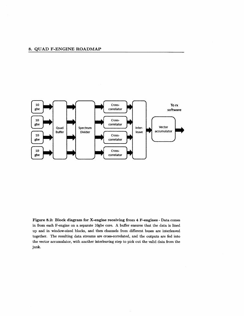
8. QUAD F-ENGINE ROADMAP
Figure 8.2: Block diagram for X-engine receiving from 4 F-engines - Data comes
in from each F-engine on a separate 10gbe core. A buffer ensures that the data is lined
up and in window-sized blocks, and then channels from different buses are interleaved
together. The resulting data streams are cross-correlated, and the outputs are fed into
the vector accumulator, with another interleaving step to pick out the valid data from the
junk.
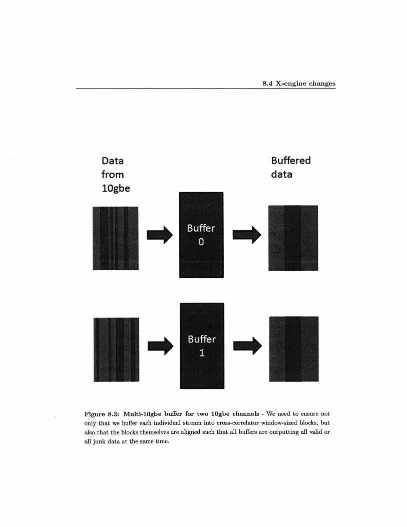
8.4 X-engine changes
Data Bufferedfrom data10gbe
Buffer0
Buffer
1
Figure 8.3: Multi-10gbe buffer for two 10gbe channels - We need to ensure not
only that we buffer each individual stream into cross-correlator window-sized blocks, but
also that the blocks themselves are aligned such that all buffers are outputting all valid or
all junk data at the same time.
10sibe

8. QUAD F-ENGINE ROADMAP
only A(A + 1)/2 output points are needed to represent the baselines. By increasing
the accumulation length B, we can reduce the duty cycle of the valid output data
to a point where each cross-correlator has a duty cycle of less than or equal to 1/4.
Then, with some delays and a multiplexer, we can funnel all of the data into the vector
accumulator. Solving
1 > A(A+ 1)/2
4- AB
we find B > 2(A + 1). In a design with four F-engines outputting 32 channels
each, we have A = 128. Thus, the internal cross-correlator accumulation length B we'll
need here is 258. For the full 256 channel design, we'll need B to be 514. This change
in accumulation length will require appropriate parametric changes in the F-engine
transpose and the X-engine's 10gbe buffer and cross-correlator.
8.5 Receiving software changes
The receiving software should undergo mostly parameteric changes, though as discussed
in section 7.5, the further increase in channels will mean an increase in minimum vector
accumulation length as well under the current system. If we can speed up the rate at
which corrtx.py can retrieve data from the vector accumulator, then we can loosen the
minimum vector accumulation length requirement. One idea to accomplish this would
be to rewrite corr.tx.py in C. As C runs much faster than Python, the hope would be
that the program could retrieve the data much more quickly.
9
Conclusion
9.1 Summary of Results
This thesis has covered the details of how I implemented the various subsystems of the
digital signal processing backend of a 32-channel interferometer. In chapter 2, I covered
the F-engine, detailing how data was taken in from the ADC, Fourier transformed,
rearranged to suit the X-engine's input, and sent out via 10-Gigabit ethernet. In
chapter 3, I discussed the X-engine, including how data is taken in from 10-Gigabit
ethernet, buffered, cross-correlated, and time-averaged. In chapter 4, I covered the
transmitting and receiving software, which take the data from the various X-engines,
get it onto a computer, and recombine it to create the full output in a useful form.
Chapter 5 deatiled the ROACH viewer, which allows us to view data inside the
F-engine in real time and make adjustments to preserve signal integrity. Chapter 6
covered the swapper, which suppresses cross-talk between the ADC channels.
After the 32-channel design, I described how I expanded its capabilities to process
64 channels in chapter 7, covering the bottlenecks in the system that forced us to make
tradeoffs and each change made to the subsystems. Finally, I left a road map of the
changes needed to make a design using four F-engines rather than one in chapter 8,
allowing us to process up to 256 channels.
9.2 Future Work
With the success of the 64-channel design, the next logical step is to scale up to the
four F-engine, four X-engine design. Although I have laid out some guidelines for

9. CONCLUSION
how to begin doing this, doubtless there will be unforeseen problems which I have full
faith that MIT cleverness will find ways around. The result waiting once this eight
ROACH design is implemented is a system capable of processing 256 input channels.
Beyond that, our lab has a 12-input, 10-Gigabit ethernet switch that will allow us to
connect even more ROACHes together to make even bigger designs. Another recent
development is ROACH 2, a new board CASPER has in production with even more
hardware resources, allowing the design to evolve not only in efficiency but also in raw
computing power per FPGA.
Bibliography
[1] M. Tegmark and M. Zaldarriaga. Omniscopes: Large Area Telescope Arrays
with only N log N Computational Cost. Phys. Rev. D, 82(103501), 2010.
[arXiv:0909.0001v2 [astro-ph.CO]] 2
[2] M. Tegmark and M. Zaldarriaga.The Fast Fourier Transform Telescope.
Phys.Rev.D79:083530,2009. [arXiv:0805.4414v2 [astro-ph]] 2
[3] N. Sanchez. On the Instrumentation of the Omniscope. Masters thesis, Mas-
sachusetts Institute of Technology, Jun 2011. Retrieved from Omniscope svn. 15,24, 36, 37, 39
[4] D. Gary. Radio Astronomy Lecture 8, Physics 728. New Jersey Institute of Tech-
nology. http://web.njit.edu/ gary/728/Lecture8.html 10